EP2194567A1 - Cleaning method of semiconductor wafer - Google Patents
Cleaning method of semiconductor wafer Download PDFInfo
- Publication number
- EP2194567A1 EP2194567A1 EP09014689A EP09014689A EP2194567A1 EP 2194567 A1 EP2194567 A1 EP 2194567A1 EP 09014689 A EP09014689 A EP 09014689A EP 09014689 A EP09014689 A EP 09014689A EP 2194567 A1 EP2194567 A1 EP 2194567A1
- Authority
- EP
- European Patent Office
- Prior art keywords
- cleaning
- wax
- wafer
- cleaning method
- microbubbles
- Prior art date
- Legal status (The legal status is an assumption and is not a legal conclusion. Google has not performed a legal analysis and makes no representation as to the accuracy of the status listed.)
- Granted
Links
Images

Classifications
-
- H—ELECTRICITY
- H10—SEMICONDUCTOR DEVICES; ELECTRIC SOLID-STATE DEVICES NOT OTHERWISE PROVIDED FOR
- H10P—GENERIC PROCESSES OR APPARATUS FOR THE MANUFACTURE OR TREATMENT OF DEVICES COVERED BY CLASS H10
- H10P50/00—Etching of wafers, substrates or parts of devices
-
- H—ELECTRICITY
- H10—SEMICONDUCTOR DEVICES; ELECTRIC SOLID-STATE DEVICES NOT OTHERWISE PROVIDED FOR
- H10P—GENERIC PROCESSES OR APPARATUS FOR THE MANUFACTURE OR TREATMENT OF DEVICES COVERED BY CLASS H10
- H10P70/00—Cleaning of wafers, substrates or parts of devices
- H10P70/50—Cleaning of wafers, substrates or parts of devices characterised by the part to be cleaned
- H10P70/56—Cleaning of wafer backside
-
- B—PERFORMING OPERATIONS; TRANSPORTING
- B08—CLEANING
- B08B—CLEANING IN GENERAL; PREVENTION OF FOULING IN GENERAL
- B08B3/00—Cleaning by methods involving the use or presence of liquid or steam
- B08B3/003—Cleaning involving contact with foam
-
- B—PERFORMING OPERATIONS; TRANSPORTING
- B08—CLEANING
- B08B—CLEANING IN GENERAL; PREVENTION OF FOULING IN GENERAL
- B08B3/00—Cleaning by methods involving the use or presence of liquid or steam
- B08B3/04—Cleaning involving contact with liquid
- B08B3/10—Cleaning involving contact with liquid with additional treatment of the liquid or of the object being cleaned, e.g. by heat, by electricity or by vibration
- B08B3/102—Cleaning involving contact with liquid with additional treatment of the liquid or of the object being cleaned, e.g. by heat, by electricity or by vibration with means for agitating the liquid
-
- B—PERFORMING OPERATIONS; TRANSPORTING
- B08—CLEANING
- B08B—CLEANING IN GENERAL; PREVENTION OF FOULING IN GENERAL
- B08B3/00—Cleaning by methods involving the use or presence of liquid or steam
- B08B3/04—Cleaning involving contact with liquid
- B08B3/10—Cleaning involving contact with liquid with additional treatment of the liquid or of the object being cleaned, e.g. by heat, by electricity or by vibration
- B08B3/12—Cleaning involving contact with liquid with additional treatment of the liquid or of the object being cleaned, e.g. by heat, by electricity or by vibration by sonic or ultrasonic vibrations
-
- H—ELECTRICITY
- H10—SEMICONDUCTOR DEVICES; ELECTRIC SOLID-STATE DEVICES NOT OTHERWISE PROVIDED FOR
- H10P—GENERIC PROCESSES OR APPARATUS FOR THE MANUFACTURE OR TREATMENT OF DEVICES COVERED BY CLASS H10
- H10P70/00—Cleaning of wafers, substrates or parts of devices
- H10P70/10—Cleaning before device manufacture, i.e. Begin-Of-Line process
- H10P70/15—Cleaning before device manufacture, i.e. Begin-Of-Line process by wet cleaning only
Definitions
- the present invention relates to a cleaning method carried out in a step of processing a semiconductor wafer of, for example, silicon.
- a semiconductor wafer (substrate) used in a semiconductor device is produced by processing an ingot block, which is grown by the Czochralski method or the floating zone method, into a mirror-surface-like thin plate.
- processing steps thereof mainly, (1) a slicing step of slicing the ingot block into wafers, (2) a beveling step of beveling an outer peripheral part of the sliced wafers, (3) a planarization step of planarizing the beveled wafers by using, for example, lapping or surface grinding, (4) an etching step for removing processing distortion of the planarized wafers, (5) a polishing step of polishing both surfaces or one surface of each of the etched wafers, (6) a thermal treatment step, an inspection step, various cleaning steps etc. are carried out.
- Patent Document 1 Japanese Unexamined Patent Application Publication No. 8-213356
- the present inventor has found out a problematic point that, in the cleaning method of the conventional techniques, the wax exfoliated as solid matters without being dissolved re-adheres onto the wafer as particles, contaminates the wafer, and causes clogging of a filter of a cleaning bath.
- the present inventors keenly examined and, as a result, found out that the wax adhering to the surface of the wafer can be uniformly removed while completely dissolving the wax into cleaning liquid without exfoliating the wax as solid matters by cleaning the wafer by using the cleaning liquid containing microbubbles, and accomplished the present invention.
- the present invention relates to a cleaning method of removing wax, which is adhering to a semiconductor wafer surface, by using cleaning liquid, the cleaning method characterized in that the cleaning liquid contains microbubbles.
- the present invention relates to the cleaning method, wherein the cleaning liquid contains an alkaline component and a surfactant.
- the present invention relates to the cleaning method, wherein the alkaline component is ammonia or organic ammonium hydroxide.
- the present invention relates to the cleaning method, wherein the semiconductor wafer is a silicon wafer.
- the cleaning liquid containing microbubbles by using the cleaning liquid containing microbubbles, the wax adhering to the surface of the wafer can be uniformly removed while dissolving in the cleaning liquid without exfoliating as solid matters, and the risk of re-contaminating the wafer by the particles generated by the wax which is exfoliated as solid matters in a wax removal process can be lowered.
- the present invention relates to a cleaning method of removing wax that adheres to a semiconductor wafer surface by using a cleaning liquid, the cleaning method characterized in that the cleaning liquid contains microbubbles.
- the material includes various materials used in conventional semiconductor fabrication. Specifically, the material includes Si, Ge, As, or a composite material thereof.
- the shape of the wafer includes the shapes formed during various processing steps which are conventional publicly-known various shapes. Preferably, silicon wafers in the stages of normal silicon wafer fabrication steps are included.
- the wax serving as a removal target is the wax which is used in a polishing step, etc. of a normal semiconductor wafer, no particular limitation is imposed also on the type thereof, and the wax generally comprises a wax component of a wax-like substance, a resin component, and an additive.
- the wax component for controlling viscosity, extension, and flexibility which mainly relate to polishing accuracy, include natural-based substances such as bees wax, oils and fats, carnauba, sumac wax, and paraffin and synthetic-based substances such as polyethylene glycol and polypropylene glycol.
- Examples of the resin component for controlling adhesion force, resistance to shock, hardness, etc., which mainly relate to retention force, include natural-based substances such as shellac, rosin, and pitch and synthetic-based substances such as vinyl acetate, nylon, acrylic, and various polymers.
- Examples of the additive for controlling cleaning performance, antioxidation, thermal resistance, wettability, etc. include various surfactants.
- the application form thereof is also not particularly limited, and examples thereof include spray wax, solid wax, and coating agents.
- a cleaning liquid can be used without no particular limitation as long as the cleaning liquid is used for removing the wax, and, specifically, an aqueous liquid which is advantageous in the point of removal performance of oils and fats, resins, particles, etc. and containing an alkaline component and surfactant is preferred.
- alkaline component examples include alkali metal hydroxide such as lithium hydroxide, sodium hydroxide, and potassium hydroxide; alkaline-earth metal hydroxide such as calcium hydroxide, magnesium hydroxide, and barium hydroxide; inorganic ammonium hydroxide such as ammonia and hydroxylamine; organic ammonium hydroxide such as monomethylammonium hydroxide, dimethylammonium hydroxide, trimethylammonium hydroxide, tetramethylammonium hydroxide, tetraethylammonium hydroxide, (n- or i-) tetrapropylammonium hydroxide, (n-, i-, or t-) tetrabutylammonium hydroxide, tetrapentylammonium hydroxide, tetrahexylammonium hydroxide, and choline; and mixtures thereof.
- alkali metal hydroxide such as lithium hydroxide, sodium hydroxide, and potassium
- the surfactant is added for improving the solubility of the wax which is the removal target, and a suitable surfactant can be selected in accordance with the wax which is the removal target.
- a suitable surfactant include a nonionic surfactant, anionic surfactant, cationic surfactant, ampholytic surfactant, and mixtures thereof.
- nonionic surfactant examples include an alkylene oxide added type nonionic surfactant and a polyhydric alcohol type nonionic surfactant.
- alkylene oxide added type nonionic surfactant examples include higher alcohol, alkylphenol, higher fatty acid, higher alkylamine, or the like to which alkylene oxide (for example, ethylene oxide (hereinafter, abbreviated as EO), propylene oxide, butylene oxide, hereinafter, the same) is directly added.
- alkylene oxide for example, ethylene oxide (hereinafter, abbreviated as EO), propylene oxide, butylene oxide, hereinafter, the same
- polyhydric alcohol type nonionic surfactant examples include polyhydric alcohol fatty acid ester, polyhydric alcohol alkyl ether, fatty acid alkanolamide etc.
- anionic surfactant examples include carboxylic acids (for example, saturated or unsaturated fatty acids having carbon numbers of 8 to 22) or salts thereof, sulfuric ester salts (for example, higher alcohol sulfuric ester salts (for example, sulfuric ester salts of aliphatic alcohol having carbon numbers of 8 to 18), higher alkyl ether sulfuric ester salts (for example, sulfuric ester salts of EO (1 to 10 mols) adduct of aliphatic alcohol having carbon numbers of 8 to 18), sulfate oil (for example, salts obtained by sulfating and neutralizing natural unsaturated oil and fat or unsaturated wax without modification), fatty acid ester sulfate (for example, salts obtained by sulfating and neutralizing lower alcohol ester of unsaturated fatty acids), sulfated olefin (for example, salts obtained by sulfating and neutralizing olefin having carbon numbers of 12 to 18), sulfonate (for example, al
- salts examples include alkali metal (sodium, potassium, etc.) salts, alkaline-earth metal (calcium, magnesium, etc.) salts, ammonium salts, alkylamine salts, and alkanolamine salts.
- cationic surfactant examples include quaternary ammonium salts such as tetraalkylammonium salts, alkylpyridinium salts, and amine salts (for example, inorganic acid salts of higher amine such as lauryl amine).
- ampholytic surfactant examples include amino acid type ampholytic surfactants (for example, sodium propionate of higher alkylamine (carbon numbers of 12 to 18)), sulfuric ester salt type ampholytic surfactants (for example, sulfuric ester sodium salts of higher alkylamine (carbon numbers of 8 to 18)), and sulfonate type ampholytic surfactants such as pentadecyl sulfotaurine.
- amino acid type ampholytic surfactants for example, sodium propionate of higher alkylamine (carbon numbers of 12 to 18)
- sulfuric ester salt type ampholytic surfactants for example, sulfuric ester sodium salts of higher alkylamine (carbon numbers of 8 to 18)
- sulfonate type ampholytic surfactants such as pentadecyl sulfotaurine.
- the used amount of the surfactant is normally 30% or less, preferably 1 to 20%, based on the total weight of the cleaning agent.
- the aqueous liquid in which the above described alkaline component and the surfactant are dissolved is preferably ultrapure water from the viewpoint of prevention of wafer contamination.
- the species of the gas of the microbubbles is not particularly limited; however, specific examples thereof include air, hydrogen, helium, nitrogen, oxygen, and argon.
- the microbubbles of the present invention include not only a single gas component, but also those comprising two or more gas components. Specifically, examples thereof include two or more species of gas components selected from a group consisting of air, hydrogen, helium, nitrogen, oxygen, and argon.
- the preparation method of the microbubbles is also not particularly limited, and the microbubbles can be generated in the cleaning liquid by introducing a gas by using a publicly known microbubble generating method or generating device.
- a publicly known microbubble generating method various methods described in publicly known documents can be applied (for example, " The World of Microbubbles" written by Satoshi Ueyama and Makoto Miyamoto, Kogyo Chosakai Publishing, Inc. (2006 )).
- Examples of the microbubble generating device include a high-speed shear flow type microbubble generating device.
- the generating conditions of the microbubbles used in the cleaning method of the present invention and the amount of the generated microbubbles are also not particularly limited. Based on the volume and shape of the used cleaning device, the number of silicon wafers, installation method, the temperature of the cleaning liquid, cleaning time, and other additives of the cleaning liquid, a microbubble generating amount in a suitable range can be arbitrarily selected.
- the position where the microbubbles are generated is also not particularly limited, and a nozzle part of the microbubbles can be provided at any position of a cleaning container.
- a suitable position can be arbitrarily selected based on the volume and shape of the used cleaning device, the number of silicon wafers, the installation method, the temperature of the cleaning liquid, cleaning time, and other additives of the cleaning liquid. Specifically, examples thereof include a bottom part, a side-surface part, and an upper part of the cleaning container and a plurality of parts thereof.
- a method in which microbubbles are generated in a container which is different from the cleaning container, and then they are introduced into the cleaning container by using a conveying pump can be also employed.
- a method in which the cleaning container and a container for producing microbubble water are coupled to each other by circulation piping, and it is kept being circulated by a conveying pump can be also employed.
- a method in which the microbubble generating device is installed at an intermediate part of conveying piping, and microbubble water is introduced to the cleaning container can be also employed.
- a wafer having one surface onto which wax was applied was prepared, and the wafer was cleaned by the method of (2).
- Skyliquid (wax produced by Nikka Seiko Co. Ltd. (hydrogenerated rosin + isopropyl alcohol + toluene)) was applied as wax onto an 8-inch P-type silicon wafer.
- a mirror surface of the silicon wafer was upwardly set in a spin coater, and, while rotating at 3000 rpm, 3 mL of the stock solution of skyliquid was measured by a pipette and poured in from the center of the substrate. After 20 seconds, the rotation was stopped, and the wafer was dried naturally.
- ANC-1 produced by Tama Chemicals Co., Ltd., 10% or less of TMAH (tetramethylammonium hydroxide) + surfactant
- TMAH tetramethylammonium hydroxide + surfactant
- microbubble generating device M2-MS/PTFE type, produced by Nanoplanet Research Institute Corporation
- M2-MS/PTFE type produced by Nanoplanet Research Institute Corporation
- Air was used as the gas for the bubbles.
- the silicon wafer having the surface onto which the wax was applied was immersed therein. During the immersion, the microbubbles were kept being generated.
- the wafer was immersed for predetermined time (for 1, 3, 5, or 10 minutes)
- the wafer was immersed in an ultrapure water rinse bath for one minute, and the chemical liquid was rinsed off. Then, the wafer was pulled up and dried by blowing dry air onto the wafer surfaces.
- FIG. 1 photos
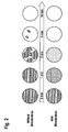
- FIG. 2 schematic drawings
- the wax was exfoliated as particles from the periphery. Therefore, it was found out that the removed manner of the wax was non-uniform and uneven. Therefore, it can be said that the possibility that the wax partially remains is high.
- the wax was exfoliated in the state of solid matters, and it can be said that the risk of particle increase and clogging of the filter is high.
- the cleaning method of the present invention is capable of efficiently removing the wax adhering to a wafer in a fabrication process of a semiconductor substrate; therefore, the cleaning method significantly contributes to this field.
Landscapes
- Cleaning Or Drying Semiconductors (AREA)
Abstract
Description
- The present invention relates to a cleaning method carried out in a step of processing a semiconductor wafer of, for example, silicon.
- A semiconductor wafer (substrate) used in a semiconductor device is produced by processing an ingot block, which is grown by the Czochralski method or the floating zone method, into a mirror-surface-like thin plate. In processing steps thereof, mainly, (1) a slicing step of slicing the ingot block into wafers, (2) a beveling step of beveling an outer peripheral part of the sliced wafers, (3) a planarization step of planarizing the beveled wafers by using, for example, lapping or surface grinding, (4) an etching step for removing processing distortion of the planarized wafers, (5) a polishing step of polishing both surfaces or one surface of each of the etched wafers, (6) a thermal treatment step, an inspection step, various cleaning steps etc. are carried out.
- Conventionally, in the polishing step of polishing one surface of a wafer, wax is applied onto one surface of the wafer that is to be polished, it is fixed to a turntable, and the other surface is polished. After this polishing step, in order to remove the wax adhering to the wafer and the particles adhered thereto during process, cleaning using bases, etc. is carried out (see Patent Document 1). In this method, the wax adhering to the wafer surface is sometimes removed in the manner that it is exfoliated instead of being completely dissolved in a cleaning liquid, and there has been a possibility of residual wax after the cleaning.
Patent Document 1 Japanese Unexamined Patent Application Publication No.8-213356 - The present inventor has found out a problematic point that, in the cleaning method of the conventional techniques, the wax exfoliated as solid matters without being dissolved re-adheres onto the wafer as particles, contaminates the wafer, and causes clogging of a filter of a cleaning bath.
- It is an object of the present invention to provide a cleaning method capable of solving the above described problem and efficiently carrying out wax removal of the wafer.
- In order to solve the above described problem, the present inventors keenly examined and, as a result, found out that the wax adhering to the surface of the wafer can be uniformly removed while completely dissolving the wax into cleaning liquid without exfoliating the wax as solid matters by cleaning the wafer by using the cleaning liquid containing microbubbles, and accomplished the present invention.
- More specifically, the present invention relates to a cleaning method of removing wax, which is adhering to a semiconductor wafer surface, by using cleaning liquid, the cleaning method characterized in that the cleaning liquid contains microbubbles.
- Furthermore, the present invention relates to the cleaning method, wherein the cleaning liquid contains an alkaline component and a surfactant.
- Furthermore, the present invention relates to the cleaning method, wherein the alkaline component is ammonia or organic ammonium hydroxide.
- Furthermore, the present invention relates to the cleaning method, wherein the semiconductor wafer is a silicon wafer.
- In the cleaning method according to the present invention, by using the cleaning liquid containing microbubbles, the wax adhering to the surface of the wafer can be uniformly removed while dissolving in the cleaning liquid without exfoliating as solid matters, and the risk of re-contaminating the wafer by the particles generated by the wax which is exfoliated as solid matters in a wax removal process can be lowered.
- Hereinafter, the present invention will be explained in detail with an embodiment.
- The present invention relates to a cleaning method of removing wax that adheres to a semiconductor wafer surface by using a cleaning liquid, the cleaning method characterized in that the cleaning liquid contains microbubbles.
- No particular limitation is imposed on the material, shape, etc. of the wafer which can be cleaned by the cleaning method of the present invention. The material includes various materials used in conventional semiconductor fabrication. Specifically, the material includes Si, Ge, As, or a composite material thereof. In the present invention, the shape of the wafer includes the shapes formed during various processing steps which are conventional publicly-known various shapes. Preferably, silicon wafers in the stages of normal silicon wafer fabrication steps are included.
- In the cleaning method of the present invention, the wax serving as a removal target is the wax which is used in a polishing step, etc. of a normal semiconductor wafer, no particular limitation is imposed also on the type thereof, and the wax generally comprises a wax component of a wax-like substance, a resin component, and an additive. Examples of the wax component for controlling viscosity, extension, and flexibility, which mainly relate to polishing accuracy, include natural-based substances such as bees wax, oils and fats, carnauba, sumac wax, and paraffin and synthetic-based substances such as polyethylene glycol and polypropylene glycol. Examples of the resin component for controlling adhesion force, resistance to shock, hardness, etc., which mainly relate to retention force, include natural-based substances such as shellac, rosin, and pitch and synthetic-based substances such as vinyl acetate, nylon, acrylic, and various polymers. Examples of the additive for controlling cleaning performance, antioxidation, thermal resistance, wettability, etc. include various surfactants. The application form thereof is also not particularly limited, and examples thereof include spray wax, solid wax, and coating agents.
- As the cleaning liquid, a cleaning liquid can be used without no particular limitation as long as the cleaning liquid is used for removing the wax, and, specifically, an aqueous liquid which is advantageous in the point of removal performance of oils and fats, resins, particles, etc. and containing an alkaline component and surfactant is preferred.
- Examples of the alkaline component include alkali metal hydroxide such as lithium hydroxide, sodium hydroxide, and potassium hydroxide; alkaline-earth metal hydroxide such as calcium hydroxide, magnesium hydroxide, and barium hydroxide; inorganic ammonium hydroxide such as ammonia and hydroxylamine; organic ammonium hydroxide such as monomethylammonium hydroxide, dimethylammonium hydroxide, trimethylammonium hydroxide, tetramethylammonium hydroxide, tetraethylammonium hydroxide, (n- or i-) tetrapropylammonium hydroxide, (n-, i-, or t-) tetrabutylammonium hydroxide, tetrapentylammonium hydroxide, tetrahexylammonium hydroxide, and choline; and mixtures thereof. Among these inorganic and organic ammonium hydroxides, ammonia, tetramethylammonium hydroxide, or choline which can obtain chemical liquid of a high cleaning level at comparatively low cost for semiconductor cleaning is preferably used.
- The surfactant is added for improving the solubility of the wax which is the removal target, and a suitable surfactant can be selected in accordance with the wax which is the removal target. Examples of the surfactant include a nonionic surfactant, anionic surfactant, cationic surfactant, ampholytic surfactant, and mixtures thereof.
- Examples of the nonionic surfactant include an alkylene oxide added type nonionic surfactant and a polyhydric alcohol type nonionic surfactant. Specific examples of the alkylene oxide added type nonionic surfactant include higher alcohol, alkylphenol, higher fatty acid, higher alkylamine, or the like to which alkylene oxide (for example, ethylene oxide (hereinafter, abbreviated as EO), propylene oxide, butylene oxide, hereinafter, the same) is directly added. Examples of the polyhydric alcohol type nonionic surfactant include polyhydric alcohol fatty acid ester, polyhydric alcohol alkyl ether, fatty acid alkanolamide etc.
- Examples of the anionic surfactant include carboxylic acids (for example, saturated or unsaturated fatty acids having carbon numbers of 8 to 22) or salts thereof, sulfuric ester salts (for example, higher alcohol sulfuric ester salts (for example, sulfuric ester salts of aliphatic alcohol having carbon numbers of 8 to 18), higher alkyl ether sulfuric ester salts (for example, sulfuric ester salts of EO (1 to 10 mols) adduct of aliphatic alcohol having carbon numbers of 8 to 18), sulfate oil (for example, salts obtained by sulfating and neutralizing natural unsaturated oil and fat or unsaturated wax without modification), fatty acid ester sulfate (for example, salts obtained by sulfating and neutralizing lower alcohol ester of unsaturated fatty acids), sulfated olefin (for example, salts obtained by sulfating and neutralizing olefin having carbon numbers of 12 to 18), sulfonate (for example, alkylbenzene sulfonate, alkyl naphthalene sulfonate, sulfosuccinic acid diester type, α-olefin (carbon numbers of 12 to 18) sulfonate), phosphoric ester salts (for example, higher alcohol (carbon number of 8 to 60) phosphoric ester salts). Examples of the salts include alkali metal (sodium, potassium, etc.) salts, alkaline-earth metal (calcium, magnesium, etc.) salts, ammonium salts, alkylamine salts, and alkanolamine salts.
- Examples of the cationic surfactant include quaternary ammonium salts such as tetraalkylammonium salts, alkylpyridinium salts, and amine salts (for example, inorganic acid salts of higher amine such as lauryl amine).
- Examples of the ampholytic surfactant include amino acid type ampholytic surfactants (for example, sodium propionate of higher alkylamine (carbon numbers of 12 to 18)), sulfuric ester salt type ampholytic surfactants (for example, sulfuric ester sodium salts of higher alkylamine (carbon numbers of 8 to 18)), and sulfonate type ampholytic surfactants such as pentadecyl sulfotaurine.
- The used amount of the surfactant is normally 30% or less, preferably 1 to 20%, based on the total weight of the cleaning agent.
- The aqueous liquid in which the above described alkaline component and the surfactant are dissolved is preferably ultrapure water from the viewpoint of prevention of wafer contamination.
- In the cleaning method of the present invention, the species of the gas of the microbubbles is not particularly limited; however, specific examples thereof include air, hydrogen, helium, nitrogen, oxygen, and argon. The microbubbles of the present invention include not only a single gas component, but also those comprising two or more gas components. Specifically, examples thereof include two or more species of gas components selected from a group consisting of air, hydrogen, helium, nitrogen, oxygen, and argon.
- The preparation method of the microbubbles is also not particularly limited, and the microbubbles can be generated in the cleaning liquid by introducing a gas by using a publicly known microbubble generating method or generating device. As the microbubbles generating method, various methods described in publicly known documents can be applied (for example, "The World of Microbubbles" written by Satoshi Ueyama and Makoto Miyamoto, Kogyo Chosakai Publishing, Inc. (2006)). Examples of the microbubble generating device include a high-speed shear flow type microbubble generating device.
- The generating conditions of the microbubbles used in the cleaning method of the present invention and the amount of the generated microbubbles are also not particularly limited. Based on the volume and shape of the used cleaning device, the number of silicon wafers, installation method, the temperature of the cleaning liquid, cleaning time, and other additives of the cleaning liquid, a microbubble generating amount in a suitable range can be arbitrarily selected.
- The position where the microbubbles are generated is also not particularly limited, and a nozzle part of the microbubbles can be provided at any position of a cleaning container. A suitable position can be arbitrarily selected based on the volume and shape of the used cleaning device, the number of silicon wafers, the installation method, the temperature of the cleaning liquid, cleaning time, and other additives of the cleaning liquid. Specifically, examples thereof include a bottom part, a side-surface part, and an upper part of the cleaning container and a plurality of parts thereof.
- A method in which microbubbles are generated in a container which is different from the cleaning container, and then they are introduced into the cleaning container by using a conveying pump can be also employed. A method in which the cleaning container and a container for producing microbubble water are coupled to each other by circulation piping, and it is kept being circulated by a conveying pump can be also employed. A method in which the microbubble generating device is installed at an intermediate part of conveying piping, and microbubble water is introduced to the cleaning container can be also employed.
- In the above described embodiment, the explanation is given on the assumption of a mode in which the wafer is immersed in the cleaning container filled with the cleaning liquid; however, shower cleaning, spray cleaning, etc. may be used. Also, cleaning can be carried out while using ultrasonic waves in combination.
- Hereinafter, the present invention will be explained in more detail based on an example.
- In accordance with below (1), a wafer having one surface onto which wax was applied was prepared, and the wafer was cleaned by the method of (2).
- Skyliquid (wax produced by Nikka Seiko Co. Ltd. (hydrogenerated rosin + isopropyl alcohol + toluene)) was applied as wax onto an 8-inch P-type silicon wafer. A mirror surface of the silicon wafer was upwardly set in a spin coater, and, while rotating at 3000 rpm, 3 mL of the stock solution of skyliquid was measured by a pipette and poured in from the center of the substrate. After 20 seconds, the rotation was stopped, and the wafer was dried naturally.
- As cleaning chemical liquid, ANC-1 (produced by Tama Chemicals Co., Ltd., 10% or less of TMAH (tetramethylammonium hydroxide) + surfactant) diluted by 20 times by ultrapure water was used, and cleaning was carried out at a liquid temperature of 20°C. Conditions of the example and a comparative example are as described below.
- One nozzle part of a microbubble generating device (M2-MS/PTFE type, produced by Nanoplanet Research Institute Corporation) was provided at a position of the bottom of a 4L cleaning bath filled with the cleaning chemical liquid, and microbubbles of 1 L/min was continuously generated and introduced. Air was used as the gas for the bubbles. After the microbubbles were introduced for five minutes, the silicon wafer having the surface onto which the wax was applied was immersed therein. During the immersion, the microbubbles were kept being generated. After the wafer was immersed for predetermined time (for 1, 3, 5, or 10 minutes), the wafer was immersed in an ultrapure water rinse bath for one minute, and the chemical liquid was rinsed off. Then, the wafer was pulled up and dried by blowing dry air onto the wafer surfaces.
- Except that the microbubbles were not generated, operations similar to those of the example were carried out.
- The wax removal state of each wafers and the state of the cleaning liquid were visually evaluated.
- The results of observing the wax removal state of the wafers are shown in
FIG. 1 (photos) andFIG. 2 (schematic drawings).
0039 - As a result of temporally observing the wax removal process, in the comparative example, the wax was exfoliated as particles from the periphery. Therefore, it was found out that the removed manner of the wax was non-uniform and uneven. Therefore, it can be said that the possibility that the wax partially remains is high. The wax was exfoliated in the state of solid matters, and it can be said that the risk of particle increase and clogging of the filter is high.
- On the other hand, when the microbubbles were added, the entire surface was uniformly dissolved, and the thickness of the wax was reduced in whole. Therefore, it was found out that the removed manner of the wax is uniform and free from unevenness. Therefore, it can be said that the possibility of partially remaining wax is low. All the wax was dissolved and removed without being exfoliated as solid matters; therefore, it can be said that the risk of particle increase and clogging of the filter is low.
- The cleaning method of the present invention is capable of efficiently removing the wax adhering to a wafer in a fabrication process of a semiconductor substrate; therefore, the cleaning method significantly contributes to this field.
-
-
FIG. 1 is photos of wafers of an example and a comparative example. -
FIG. 2 is a schematic drawing showing results of observing the state of the wafers of the example and the comparative example.
Claims (4)
- A cleaning method of removing wax, which is adhering to a semiconductor wafer surface, by using cleaning liquid, the cleaning method characterized in that the cleaning liquid contains microbubbles.
- The cleaning method described in claim 1, wherein the cleaning liquid is an aqueous liquid containing an alkaline component and a surfactant.
- The cleaning method described in claim 2, wherein the alkaline component is quaternary ammonium hydroxide.
- The cleaning method described in any of claims 1 to 3, wherein the semiconductor wafer is a silicon wafer.
Applications Claiming Priority (1)
| Application Number | Priority Date | Filing Date | Title |
|---|---|---|---|
| JP2008309283A JP2010135525A (en) | 2008-12-04 | 2008-12-04 | Method of cleaning semiconductor wafer |
Publications (2)
| Publication Number | Publication Date |
|---|---|
| EP2194567A1 true EP2194567A1 (en) | 2010-06-09 |
| EP2194567B1 EP2194567B1 (en) | 2012-08-15 |
Family
ID=42028208
Family Applications (1)
| Application Number | Title | Priority Date | Filing Date |
|---|---|---|---|
| EP09014689A Not-in-force EP2194567B1 (en) | 2008-12-04 | 2009-11-25 | Cleaning method of semiconductor wafer |
Country Status (6)
| Country | Link |
|---|---|
| US (1) | US10121649B2 (en) |
| EP (1) | EP2194567B1 (en) |
| JP (1) | JP2010135525A (en) |
| KR (1) | KR101146000B1 (en) |
| CN (2) | CN104550100A (en) |
| TW (1) | TWI409863B (en) |
Cited By (2)
| Publication number | Priority date | Publication date | Assignee | Title |
|---|---|---|---|---|
| JP2017119930A (en) * | 2015-12-28 | 2017-07-06 | 王子ホールディングス株式会社 | Cleaning method and cleaning system for paper making tools |
| CN111112217A (en) * | 2019-12-24 | 2020-05-08 | 北京航天时代激光导航技术有限责任公司 | Method for cleaning bonding wax of tool plate on upper disc of spherical reflector |
Families Citing this family (5)
| Publication number | Priority date | Publication date | Assignee | Title |
|---|---|---|---|---|
| CN103639142A (en) * | 2013-12-09 | 2014-03-19 | 天津中环领先材料技术有限公司 | Cleaning method of wax polished ceramic plates |
| CN105499228B (en) * | 2015-11-25 | 2017-08-25 | 中锗科技有限公司 | A kind of solar energy germanium wafer is packed for the cleaning method of wafer cassette |
| WO2017119350A1 (en) * | 2016-01-05 | 2017-07-13 | 富士フイルム株式会社 | Treatment liquid, method for cleaning substrate and method for manufacturing semiconductor device |
| CN107937923A (en) * | 2017-11-28 | 2018-04-20 | 东莞市四辉表面处理科技有限公司 | A kind of stainless steel wax removing agent of function admirable |
| JP2024143699A (en) * | 2023-03-30 | 2024-10-11 | 高周波熱錬株式会社 | Carrier film cleaning method and cleaning device |
Citations (4)
| Publication number | Priority date | Publication date | Assignee | Title |
|---|---|---|---|---|
| JPH08213356A (en) | 1995-01-31 | 1996-08-20 | Komatsu Electron Metals Co Ltd | Wafer cleaning method |
| WO2004053045A1 (en) * | 2002-12-12 | 2004-06-24 | Showa Denko K.K. | Cleaning agent composition, cleaning and production methods for semiconductor wafer, and semiconductor wafer |
| CN1876786A (en) * | 2006-06-30 | 2006-12-13 | 天津晶岭电子材料科技有限公司 | Cleaning solution for removing semiconductor material surface wax and organic substances and cleaning method thereof |
| KR100845966B1 (en) * | 2007-06-28 | 2008-07-11 | 주식회사 실트론 | Wafer Cleaning Method |
Family Cites Families (18)
| Publication number | Priority date | Publication date | Assignee | Title |
|---|---|---|---|---|
| JPS63274149A (en) * | 1987-05-06 | 1988-11-11 | Mitsubishi Gas Chem Co Inc | Semiconductor treatment |
| DE69102311T2 (en) | 1990-03-07 | 1994-09-29 | Hitachi Ltd | Device and method for surface cleaning. |
| JPH11354476A (en) | 1998-06-10 | 1999-12-24 | Memc Kk | Storage method of silicon wafer |
| US6417147B2 (en) * | 2000-02-29 | 2002-07-09 | Showa Denko K.K. | Cleaning agent composition, method for cleaning and use thereof |
| US6418942B1 (en) * | 2000-03-10 | 2002-07-16 | Donald Gray | Solvent and aqueous decompression processing system |
| US6310019B1 (en) * | 2000-07-05 | 2001-10-30 | Wako Pure Chemical Industries, Ltd. | Cleaning agent for a semi-conductor substrate |
| TWI295076B (en) * | 2002-09-19 | 2008-03-21 | Dongwoo Fine Chem Co Ltd | Washing liquid for semiconductor substrate and method of producing semiconductor device |
| US7373941B2 (en) * | 2003-03-28 | 2008-05-20 | Taiwan Semiconductor Manufacturing Co. Ltd | Wet cleaning cavitation system and method to remove particulate wafer contamination |
| KR100511915B1 (en) * | 2003-05-15 | 2005-09-02 | 주식회사 하이닉스반도체 | Method for cleaning polishing wafer |
| KR20050065312A (en) * | 2003-12-25 | 2005-06-29 | 마츠시타 덴끼 산교 가부시키가이샤 | Cleansing method of semiconductor wafer |
| US7392814B2 (en) * | 2004-12-24 | 2008-07-01 | Dainippon Screen Mfg. Co., Ltd. | Substrate processing apparatus and method |
| JP4613744B2 (en) | 2005-08-10 | 2011-01-19 | 株式会社Sumco | Cleaning method of silicon wafer |
| KR20070018689A (en) * | 2005-08-10 | 2007-02-14 | 가부시키가이샤 섬코 | Silicon Wafer Cleaning Method |
| JP2007098361A (en) * | 2005-10-07 | 2007-04-19 | Sharp Corp | Substrate processing equipment |
| JP2008103701A (en) * | 2006-09-19 | 2008-05-01 | Siltronic Ag | Wet treatment method of silicon wafer |
| CN101169597A (en) | 2006-10-27 | 2008-04-30 | 安集微电子(上海)有限公司 | Photoresist detergent |
| SG144040A1 (en) | 2006-12-27 | 2008-07-29 | Siltronic Ag | Cleaning liquid and cleaning method for electronic material |
| JP2008182188A (en) * | 2006-12-27 | 2008-08-07 | Siltronic Ag | Cleaning liquid for electronic materials and cleaning method |
-
2008
- 2008-12-04 JP JP2008309283A patent/JP2010135525A/en active Pending
-
2009
- 2009-11-05 CN CN201410646025.9A patent/CN104550100A/en active Pending
- 2009-11-05 KR KR1020090106570A patent/KR101146000B1/en not_active Expired - Fee Related
- 2009-11-05 CN CN200910211834A patent/CN101745507A/en active Pending
- 2009-11-25 EP EP09014689A patent/EP2194567B1/en not_active Not-in-force
- 2009-12-01 US US12/592,706 patent/US10121649B2/en active Active
- 2009-12-02 TW TW098141131A patent/TWI409863B/en not_active IP Right Cessation
Patent Citations (4)
| Publication number | Priority date | Publication date | Assignee | Title |
|---|---|---|---|---|
| JPH08213356A (en) | 1995-01-31 | 1996-08-20 | Komatsu Electron Metals Co Ltd | Wafer cleaning method |
| WO2004053045A1 (en) * | 2002-12-12 | 2004-06-24 | Showa Denko K.K. | Cleaning agent composition, cleaning and production methods for semiconductor wafer, and semiconductor wafer |
| CN1876786A (en) * | 2006-06-30 | 2006-12-13 | 天津晶岭电子材料科技有限公司 | Cleaning solution for removing semiconductor material surface wax and organic substances and cleaning method thereof |
| KR100845966B1 (en) * | 2007-06-28 | 2008-07-11 | 주식회사 실트론 | Wafer Cleaning Method |
Non-Patent Citations (3)
| Title |
|---|
| DATABASE EPODOC EUROPEAN PATENT OFFICE, THE HAGUE, NL; 11 July 2008 (2008-07-11), accession no. kr100845966 * |
| DATABASE EPODOC EUROPEAN PATENT OFFICE, THE HAGUE, NL; 13 December 2006 (2006-12-13), accession no. cn1876786 * |
| SATOSHI UEYAMA; MAKOTO MIYAMOTO: "The World of Microbubbles", 2006, KOGYO CHOSAKAI PUBLISHING, INC. |
Cited By (2)
| Publication number | Priority date | Publication date | Assignee | Title |
|---|---|---|---|---|
| JP2017119930A (en) * | 2015-12-28 | 2017-07-06 | 王子ホールディングス株式会社 | Cleaning method and cleaning system for paper making tools |
| CN111112217A (en) * | 2019-12-24 | 2020-05-08 | 北京航天时代激光导航技术有限责任公司 | Method for cleaning bonding wax of tool plate on upper disc of spherical reflector |
Also Published As
| Publication number | Publication date |
|---|---|
| JP2010135525A (en) | 2010-06-17 |
| CN101745507A (en) | 2010-06-23 |
| TWI409863B (en) | 2013-09-21 |
| US10121649B2 (en) | 2018-11-06 |
| US20100139711A1 (en) | 2010-06-10 |
| KR20100064328A (en) | 2010-06-14 |
| KR101146000B1 (en) | 2012-05-16 |
| TW201023254A (en) | 2010-06-16 |
| EP2194567B1 (en) | 2012-08-15 |
| CN104550100A (en) | 2015-04-29 |
Similar Documents
| Publication | Publication Date | Title |
|---|---|---|
| EP2194567B1 (en) | Cleaning method of semiconductor wafer | |
| TWI551678B (en) | Substrate cleaning solution for semiconductor device and substrate for semiconductor device | |
| KR101520917B1 (en) | Texturing and cleaning agent for the surface treatment of wafers and use thereof | |
| CN101337227B (en) | Method for cleaning semiconductor chip using cleaning solution | |
| US6988936B2 (en) | Surface preparation for receiving processing treatments | |
| TW201343904A (en) | Cleaning method for semiconductor device and substrate for semiconductor device | |
| TW200426933A (en) | Cleaning method, method for removing foreign particle, cleaning apparatus and cleaning liquid | |
| JP2008182188A (en) | Cleaning liquid for electronic materials and cleaning method | |
| CN105364699B (en) | Chemical mechanical polishing method and chemical mechanical polishing equipment | |
| JP2008166804A (en) | Cleaning method for solar cell substrate | |
| CN101211995A (en) | Method for cleaning solar cell substrates | |
| KR102172311B1 (en) | Method for forming a protective film on a semiconductor substrate | |
| TW202411414A (en) | Detergent composition for adhesive | |
| KR20170044234A (en) | A cleaning device using the micro bubbles for silicone wafer and cleaning method using the same | |
| US7700535B1 (en) | Wafer/Ingot cleaning in wire saw cutting comprising an ethoxylated alcohol/polyalkylsiloxane mixture | |
| JP2005075924A (en) | Silica scale remover | |
| WO2023120016A1 (en) | Method for cleaning semiconductor wafer and method for producing semiconductor wafer | |
| KR20210046883A (en) | Cutting oil and slurry for wire sawing apparatus comprising the same | |
| JP7517530B1 (en) | Method for cleaning semiconductor wafers | |
| JP2006041065A (en) | Solid spray cleaning method | |
| JP4376022B2 (en) | Silica scale remover | |
| Cahue et al. | Design of “Soft” Cleaning Processes for Emerging Substrates via Stimuli Responsive Chemistry | |
| CN120109006A (en) | A novel method for preparing ultra-thin functional layer structure of composite substrate | |
| CN119260585A (en) | Wax polishing process and polishing device for silicon wafer | |
| JP2006179593A (en) | Method of cleaning and drying semiconductor wafer |
Legal Events
| Date | Code | Title | Description |
|---|---|---|---|
| PUAI | Public reference made under article 153(3) epc to a published international application that has entered the european phase |
Free format text: ORIGINAL CODE: 0009012 |
|
| 17P | Request for examination filed |
Effective date: 20091125 |
|
| AK | Designated contracting states |
Kind code of ref document: A1 Designated state(s): AT BE BG CH CY CZ DE DK EE ES FI FR GB GR HR HU IE IS IT LI LT LU LV MC MK MT NL NO PL PT RO SE SI SK SM TR |
|
| AX | Request for extension of the european patent |
Extension state: AL BA RS |
|
| 17Q | First examination report despatched |
Effective date: 20100712 |
|
| GRAP | Despatch of communication of intention to grant a patent |
Free format text: ORIGINAL CODE: EPIDOSNIGR1 |
|
| RIC1 | Information provided on ipc code assigned before grant |
Ipc: H01L 21/02 20060101AFI20120316BHEP Ipc: B08B 3/00 20060101ALI20120316BHEP |
|
| GRAS | Grant fee paid |
Free format text: ORIGINAL CODE: EPIDOSNIGR3 |
|
| GRAA | (expected) grant |
Free format text: ORIGINAL CODE: 0009210 |
|
| AK | Designated contracting states |
Kind code of ref document: B1 Designated state(s): AT BE BG CH CY CZ DE DK EE ES FI FR GB GR HR HU IE IS IT LI LT LU LV MC MK MT NL NO PL PT RO SE SI SK SM TR |
|
| REG | Reference to a national code |
Ref country code: AT Ref legal event code: REF Ref document number: 571210 Country of ref document: AT Kind code of ref document: T Effective date: 20120815 Ref country code: CH Ref legal event code: EP Ref country code: GB Ref legal event code: FG4D |
|
| REG | Reference to a national code |
Ref country code: IE Ref legal event code: FG4D |
|
| REG | Reference to a national code |
Ref country code: DE Ref legal event code: R096 Ref document number: 602009008916 Country of ref document: DE Effective date: 20121011 |
|
| REG | Reference to a national code |
Ref country code: NL Ref legal event code: VDEP Effective date: 20120815 |
|
| REG | Reference to a national code |
Ref country code: AT Ref legal event code: MK05 Ref document number: 571210 Country of ref document: AT Kind code of ref document: T Effective date: 20120815 |
|
| PG25 | Lapsed in a contracting state [announced via postgrant information from national office to epo] |
Ref country code: CY Free format text: LAPSE BECAUSE OF FAILURE TO SUBMIT A TRANSLATION OF THE DESCRIPTION OR TO PAY THE FEE WITHIN THE PRESCRIBED TIME-LIMIT Effective date: 20120815 Ref country code: FI Free format text: LAPSE BECAUSE OF FAILURE TO SUBMIT A TRANSLATION OF THE DESCRIPTION OR TO PAY THE FEE WITHIN THE PRESCRIBED TIME-LIMIT Effective date: 20120815 Ref country code: IS Free format text: LAPSE BECAUSE OF FAILURE TO SUBMIT A TRANSLATION OF THE DESCRIPTION OR TO PAY THE FEE WITHIN THE PRESCRIBED TIME-LIMIT Effective date: 20121215 Ref country code: HR Free format text: LAPSE BECAUSE OF FAILURE TO SUBMIT A TRANSLATION OF THE DESCRIPTION OR TO PAY THE FEE WITHIN THE PRESCRIBED TIME-LIMIT Effective date: 20120815 Ref country code: LT Free format text: LAPSE BECAUSE OF FAILURE TO SUBMIT A TRANSLATION OF THE DESCRIPTION OR TO PAY THE FEE WITHIN THE PRESCRIBED TIME-LIMIT Effective date: 20120815 Ref country code: AT Free format text: LAPSE BECAUSE OF FAILURE TO SUBMIT A TRANSLATION OF THE DESCRIPTION OR TO PAY THE FEE WITHIN THE PRESCRIBED TIME-LIMIT Effective date: 20120815 Ref country code: NO Free format text: LAPSE BECAUSE OF FAILURE TO SUBMIT A TRANSLATION OF THE DESCRIPTION OR TO PAY THE FEE WITHIN THE PRESCRIBED TIME-LIMIT Effective date: 20121115 |
|
| PG25 | Lapsed in a contracting state [announced via postgrant information from national office to epo] |
Ref country code: BE Free format text: LAPSE BECAUSE OF FAILURE TO SUBMIT A TRANSLATION OF THE DESCRIPTION OR TO PAY THE FEE WITHIN THE PRESCRIBED TIME-LIMIT Effective date: 20120815 Ref country code: PT Free format text: LAPSE BECAUSE OF FAILURE TO SUBMIT A TRANSLATION OF THE DESCRIPTION OR TO PAY THE FEE WITHIN THE PRESCRIBED TIME-LIMIT Effective date: 20121217 Ref country code: GR Free format text: LAPSE BECAUSE OF FAILURE TO SUBMIT A TRANSLATION OF THE DESCRIPTION OR TO PAY THE FEE WITHIN THE PRESCRIBED TIME-LIMIT Effective date: 20121116 Ref country code: SI Free format text: LAPSE BECAUSE OF FAILURE TO SUBMIT A TRANSLATION OF THE DESCRIPTION OR TO PAY THE FEE WITHIN THE PRESCRIBED TIME-LIMIT Effective date: 20120815 Ref country code: SE Free format text: LAPSE BECAUSE OF FAILURE TO SUBMIT A TRANSLATION OF THE DESCRIPTION OR TO PAY THE FEE WITHIN THE PRESCRIBED TIME-LIMIT Effective date: 20120815 Ref country code: PL Free format text: LAPSE BECAUSE OF FAILURE TO SUBMIT A TRANSLATION OF THE DESCRIPTION OR TO PAY THE FEE WITHIN THE PRESCRIBED TIME-LIMIT Effective date: 20120815 Ref country code: LV Free format text: LAPSE BECAUSE OF FAILURE TO SUBMIT A TRANSLATION OF THE DESCRIPTION OR TO PAY THE FEE WITHIN THE PRESCRIBED TIME-LIMIT Effective date: 20120815 |
|
| PG25 | Lapsed in a contracting state [announced via postgrant information from national office to epo] |
Ref country code: NL Free format text: LAPSE BECAUSE OF FAILURE TO SUBMIT A TRANSLATION OF THE DESCRIPTION OR TO PAY THE FEE WITHIN THE PRESCRIBED TIME-LIMIT Effective date: 20120815 |
|
| PG25 | Lapsed in a contracting state [announced via postgrant information from national office to epo] |
Ref country code: EE Free format text: LAPSE BECAUSE OF FAILURE TO SUBMIT A TRANSLATION OF THE DESCRIPTION OR TO PAY THE FEE WITHIN THE PRESCRIBED TIME-LIMIT Effective date: 20120815 Ref country code: DK Free format text: LAPSE BECAUSE OF FAILURE TO SUBMIT A TRANSLATION OF THE DESCRIPTION OR TO PAY THE FEE WITHIN THE PRESCRIBED TIME-LIMIT Effective date: 20120815 Ref country code: CZ Free format text: LAPSE BECAUSE OF FAILURE TO SUBMIT A TRANSLATION OF THE DESCRIPTION OR TO PAY THE FEE WITHIN THE PRESCRIBED TIME-LIMIT Effective date: 20120815 Ref country code: RO Free format text: LAPSE BECAUSE OF FAILURE TO SUBMIT A TRANSLATION OF THE DESCRIPTION OR TO PAY THE FEE WITHIN THE PRESCRIBED TIME-LIMIT Effective date: 20120815 Ref country code: ES Free format text: LAPSE BECAUSE OF FAILURE TO SUBMIT A TRANSLATION OF THE DESCRIPTION OR TO PAY THE FEE WITHIN THE PRESCRIBED TIME-LIMIT Effective date: 20121126 |
|
| PG25 | Lapsed in a contracting state [announced via postgrant information from national office to epo] |
Ref country code: IT Free format text: LAPSE BECAUSE OF FAILURE TO SUBMIT A TRANSLATION OF THE DESCRIPTION OR TO PAY THE FEE WITHIN THE PRESCRIBED TIME-LIMIT Effective date: 20120815 Ref country code: SK Free format text: LAPSE BECAUSE OF FAILURE TO SUBMIT A TRANSLATION OF THE DESCRIPTION OR TO PAY THE FEE WITHIN THE PRESCRIBED TIME-LIMIT Effective date: 20120815 |
|
| PLBE | No opposition filed within time limit |
Free format text: ORIGINAL CODE: 0009261 |
|
| STAA | Information on the status of an ep patent application or granted ep patent |
Free format text: STATUS: NO OPPOSITION FILED WITHIN TIME LIMIT |
|
| 26N | No opposition filed |
Effective date: 20130516 |
|
| PG25 | Lapsed in a contracting state [announced via postgrant information from national office to epo] |
Ref country code: BG Free format text: LAPSE BECAUSE OF FAILURE TO SUBMIT A TRANSLATION OF THE DESCRIPTION OR TO PAY THE FEE WITHIN THE PRESCRIBED TIME-LIMIT Effective date: 20121115 |
|
| REG | Reference to a national code |
Ref country code: FR Ref legal event code: ST Effective date: 20130731 |
|
| REG | Reference to a national code |
Ref country code: IE Ref legal event code: MM4A |
|
| REG | Reference to a national code |
Ref country code: DE Ref legal event code: R097 Ref document number: 602009008916 Country of ref document: DE Effective date: 20130516 |
|
| PG25 | Lapsed in a contracting state [announced via postgrant information from national office to epo] |
Ref country code: IE Free format text: LAPSE BECAUSE OF NON-PAYMENT OF DUE FEES Effective date: 20121125 |
|
| PG25 | Lapsed in a contracting state [announced via postgrant information from national office to epo] |
Ref country code: FR Free format text: LAPSE BECAUSE OF NON-PAYMENT OF DUE FEES Effective date: 20121130 Ref country code: MT Free format text: LAPSE BECAUSE OF FAILURE TO SUBMIT A TRANSLATION OF THE DESCRIPTION OR TO PAY THE FEE WITHIN THE PRESCRIBED TIME-LIMIT Effective date: 20120815 |
|
| PG25 | Lapsed in a contracting state [announced via postgrant information from national office to epo] |
Ref country code: TR Free format text: LAPSE BECAUSE OF FAILURE TO SUBMIT A TRANSLATION OF THE DESCRIPTION OR TO PAY THE FEE WITHIN THE PRESCRIBED TIME-LIMIT Effective date: 20120815 Ref country code: MC Free format text: LAPSE BECAUSE OF NON-PAYMENT OF DUE FEES Effective date: 20121130 |
|
| PG25 | Lapsed in a contracting state [announced via postgrant information from national office to epo] |
Ref country code: LU Free format text: LAPSE BECAUSE OF NON-PAYMENT OF DUE FEES Effective date: 20121125 Ref country code: SM Free format text: LAPSE BECAUSE OF FAILURE TO SUBMIT A TRANSLATION OF THE DESCRIPTION OR TO PAY THE FEE WITHIN THE PRESCRIBED TIME-LIMIT Effective date: 20120815 |
|
| REG | Reference to a national code |
Ref country code: CH Ref legal event code: PL |
|
| GBPC | Gb: european patent ceased through non-payment of renewal fee |
Effective date: 20131125 |
|
| PG25 | Lapsed in a contracting state [announced via postgrant information from national office to epo] |
Ref country code: CH Free format text: LAPSE BECAUSE OF NON-PAYMENT OF DUE FEES Effective date: 20131130 Ref country code: HU Free format text: LAPSE BECAUSE OF FAILURE TO SUBMIT A TRANSLATION OF THE DESCRIPTION OR TO PAY THE FEE WITHIN THE PRESCRIBED TIME-LIMIT Effective date: 20091125 Ref country code: LI Free format text: LAPSE BECAUSE OF NON-PAYMENT OF DUE FEES Effective date: 20131130 |
|
| PG25 | Lapsed in a contracting state [announced via postgrant information from national office to epo] |
Ref country code: GB Free format text: LAPSE BECAUSE OF NON-PAYMENT OF DUE FEES Effective date: 20131125 |
|
| PG25 | Lapsed in a contracting state [announced via postgrant information from national office to epo] |
Ref country code: MK Free format text: LAPSE BECAUSE OF FAILURE TO SUBMIT A TRANSLATION OF THE DESCRIPTION OR TO PAY THE FEE WITHIN THE PRESCRIBED TIME-LIMIT Effective date: 20120815 |
|
| PGFP | Annual fee paid to national office [announced via postgrant information from national office to epo] |
Ref country code: DE Payment date: 20231121 Year of fee payment: 15 |
|
| REG | Reference to a national code |
Ref country code: DE Ref legal event code: R119 Ref document number: 602009008916 Country of ref document: DE |
|
| PG25 | Lapsed in a contracting state [announced via postgrant information from national office to epo] |
Ref country code: DE Free format text: LAPSE BECAUSE OF NON-PAYMENT OF DUE FEES Effective date: 20250603 |