EP2187432A1 - P-type field-effect transistor and method of production - Google Patents
P-type field-effect transistor and method of production Download PDFInfo
- Publication number
- EP2187432A1 EP2187432A1 EP08169044A EP08169044A EP2187432A1 EP 2187432 A1 EP2187432 A1 EP 2187432A1 EP 08169044 A EP08169044 A EP 08169044A EP 08169044 A EP08169044 A EP 08169044A EP 2187432 A1 EP2187432 A1 EP 2187432A1
- Authority
- EP
- European Patent Office
- Prior art keywords
- layer
- effect transistor
- field
- source
- gate electrode
- Prior art date
- Legal status (The legal status is an assumption and is not a legal conclusion. Google has not performed a legal analysis and makes no representation as to the accuracy of the status listed.)
- Granted
Links
Images

Classifications
-
- H—ELECTRICITY
- H10—SEMICONDUCTOR DEVICES; ELECTRIC SOLID-STATE DEVICES NOT OTHERWISE PROVIDED FOR
- H10D—INORGANIC ELECTRIC SEMICONDUCTOR DEVICES
- H10D64/00—Electrodes of devices having potential barriers
- H10D64/20—Electrodes characterised by their shapes, relative sizes or dispositions
- H10D64/27—Electrodes not carrying the current to be rectified, amplified, oscillated or switched, e.g. gates
- H10D64/311—Gate electrodes for field-effect devices
- H10D64/411—Gate electrodes for field-effect devices for FETs
- H10D64/511—Gate electrodes for field-effect devices for FETs for IGFETs
- H10D64/512—Disposition of the gate electrodes, e.g. buried gates
- H10D64/513—Disposition of the gate electrodes, e.g. buried gates within recesses in the substrate, e.g. trench gates, groove gates or buried gates
-
- H—ELECTRICITY
- H10—SEMICONDUCTOR DEVICES; ELECTRIC SOLID-STATE DEVICES NOT OTHERWISE PROVIDED FOR
- H10D—INORGANIC ELECTRIC SEMICONDUCTOR DEVICES
- H10D30/00—Field-effect transistors [FET]
- H10D30/01—Manufacture or treatment
- H10D30/021—Manufacture or treatment of FETs having insulated gates [IGFET]
-
- H—ELECTRICITY
- H10—SEMICONDUCTOR DEVICES; ELECTRIC SOLID-STATE DEVICES NOT OTHERWISE PROVIDED FOR
- H10D—INORGANIC ELECTRIC SEMICONDUCTOR DEVICES
- H10D62/00—Semiconductor bodies, or regions thereof, of devices having potential barriers
- H10D62/10—Shapes, relative sizes or dispositions of the regions of the semiconductor bodies; Shapes of the semiconductor bodies
- H10D62/17—Semiconductor regions connected to electrodes not carrying current to be rectified, amplified or switched, e.g. channel regions
- H10D62/351—Substrate regions of field-effect devices
- H10D62/357—Substrate regions of field-effect devices of FETs
- H10D62/364—Substrate regions of field-effect devices of FETs of IGFETs
- H10D62/378—Contact regions to the substrate regions
-
- H—ELECTRICITY
- H10—SEMICONDUCTOR DEVICES; ELECTRIC SOLID-STATE DEVICES NOT OTHERWISE PROVIDED FOR
- H10D—INORGANIC ELECTRIC SEMICONDUCTOR DEVICES
- H10D64/00—Electrodes of devices having potential barriers
- H10D64/01—Manufacture or treatment
- H10D64/025—Manufacture or treatment forming recessed gates, e.g. by using local oxidation
- H10D64/027—Manufacture or treatment forming recessed gates, e.g. by using local oxidation by etching at gate locations
-
- H—ELECTRICITY
- H10—SEMICONDUCTOR DEVICES; ELECTRIC SOLID-STATE DEVICES NOT OTHERWISE PROVIDED FOR
- H10D—INORGANIC ELECTRIC SEMICONDUCTOR DEVICES
- H10D62/00—Semiconductor bodies, or regions thereof, of devices having potential barriers
- H10D62/80—Semiconductor bodies, or regions thereof, of devices having potential barriers characterised by the materials
- H10D62/82—Heterojunctions
- H10D62/824—Heterojunctions comprising only Group III-V materials heterojunctions, e.g. GaN/AlGaN heterojunctions
-
- H—ELECTRICITY
- H10—SEMICONDUCTOR DEVICES; ELECTRIC SOLID-STATE DEVICES NOT OTHERWISE PROVIDED FOR
- H10D—INORGANIC ELECTRIC SEMICONDUCTOR DEVICES
- H10D62/00—Semiconductor bodies, or regions thereof, of devices having potential barriers
- H10D62/80—Semiconductor bodies, or regions thereof, of devices having potential barriers characterised by the materials
- H10D62/85—Semiconductor bodies, or regions thereof, of devices having potential barriers characterised by the materials being Group III-V materials, e.g. GaAs
Definitions
- GaAs semiconductor technology provides transistor devices of the npn bipolar transistor and n-FET types. Circuit design and system functionality require p-type devices, especially pnp bipolar transistors or p-channel field-effect transistors, which are not provided in the GaAs technology up to now. With only n-type devices available in GaAs technology, other circuit concepts are applied at the expense of increased current consumption, larger occupied area and other shortcomings. Semiconductor circuits in silicon comprise both n-type and p-type devices, but this is not the preferred technology for power amplifiers, especially in industrial applications. Although the lacking p-type transistor components can be provided on external circuit components, a full integration of both types of transistors is desired also in GaAs technology.
- a further object is the disclosure of an efficient production method of a p-channel field-effect transistor in GaAs technology.
- the field-effect transistor is based on a layer structure that can be used to manufacture npn bipolar transistors.
- a p-doped layer which can also serve as base layer of a bipolar transistor, is divided into two separate portions by a recess, in which a gate electrode is located.
- the gate electrode is on a gate dielectric layer and controls the space charge in the channel in an n-doped layer, which can also serve as collector layer of a bipolar transistor.
- the p-channel field-effect transistor can be arranged in a layer sequence that can be used in a vertical npn bipolar transistor. Furthermore, this layer sequence can be laterally confined to form a mesa on a substrate surface.
- An n + -doped layer which can also serve as subcollector layer of a bipolar transistor, can be positioned under the mesa and be provided with an external electric connection functioning as a bulk contact of the field-effect transistor.
- FIG. 1 shows a cross-section of an embodiment of the p-channel field-effect transistor.
- An n + -layer 2 is located on an upper surface of a substrate 1, which can be especially GaAs.
- a layer sequence is arranged forming a mesa, which comprises an n-layer 3, a p-layer 4 and a further n-layer 5.
- This layer sequence can be provided for npn bipolar transistors, which can be manufactured on the same substrate.
- the field-effect transistor can use the layer sequence of a standard GaAs HBT manufacturing technology.
- the upper n-layer 5, which is shown in the cross-section of FIG. 1 is not necessary for the field-effect transistor. It could therefore be left out or removed, but it can be left on the p-layer 4 as well if the layer sequence as shown in FIG. 1 is provided in the production method.
- the p-layer 4 is divided by a trench or recess into two separate portions as shown in FIG. 1 .
- the bottom and sidewalls of the recess are covered with a relatively thin gate dielectric 6.
- source/drain contact layers 7, preferably a metal may be arranged on the surface of the portions of the p-layer 4.
- the regions that are occupied by space charge regions 8 during the operation of the transistor are indicated by the hatched areas in FIG. 1 .
- a channel region 9 is provided under the gate dielectric 6 within the lower n-layer 3 between the space charge regions 8. Since the channel region 9 is located in n-doped semiconductor material, it is provided for a p-channel field-effect transistor.
- Source/drain contacts 11 are provided for source and drain and, in this embodiment, arranged on the source/drain contact layers 7.
- the source/drain contacts 11 are preferably a metal.
- the n + -layer 2 can be provided as a subcollector layer of a vertical npn transistor.
- the n + -layer 2 can be used to provide a bulk contact.
- a bulk contact layer 12 preferably a metal
- An isolating layer 14 on the level of the n + -layer 2 can be provided as a lateral insulation of the n + -layer 2, and a further dielectric layer 15 can be provided as a passivation and electric insulation between the various electric contacts on the upper side of the device.
- the arrangement and shape of the layers, especially the gate dielectric 6, the dielectric layer 15, and the contact layers, may deviate from the example of FIG. 1 and can be varied in order to optimize the performance of the field-effect transistor.
- the field-effect transistor is especially advantageous in that the source/drain regions are formed by portions of the p-layer 4, which can also serve as the base layer of a vertical npn bipolar transistor, and the channel region is located in an n-layer 3, which can also serve as a collector layer of an npn bipolar transistor.
- the source/drain regions are completely separated from one another by the recess comprising the gate electrode and the gate dielectric. Thus there is no direct connection via p-doped semiconductor material between the two portions of the p-layer 4. In this manner, a sequence of p-doped, n-doped and p-doped semiconductor layers can be used to form a field-effect transistor of essentially lateral structure.
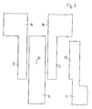
- FIG. 2 shows the layout of the electrically conducting tracks in a schematic plan view.
- the gate electrode 10 is shown to be arranged between the source/drain contacts 11, while the bulk contact 13 is arranged laterally to the other contacts.
- every contact 10, 11, 13 is electrically conductively connected with a contact pad 16, which can be used to apply an external electric connection.
- the design of the conducting tracks and contact layers can be varied according to the requirements of each individual embodiment. Thus there is a large variety of possibilities to integrate the field-effect transistor together with other devices, especially vertical bipolar transistors.
- the field-effect transistor can be manufactured within a standard GaAs technology together with vertical bipolar transistors.
- the method of production of the field-effect transistor can comprise the steps of applying an n-layer and a p-layer above a substrate of semiconductor material, especially of GaAs, the layers being preferably structured in the shape of a mesa.
- a recess or trench is etched into the p-layer in order to form two separate portions, which are not connected by p-doped semiconductor material.
- a gate dielectric is arranged on the bottom and sidewalls of the recess.
- the gate dielectric can be silicon nitride, which can be used within a standard GaAs HBT technology.
- a gate electrode, preferably formed from metal, is arranged in the recess on the gate dielectric.
- Source/drain contacts are arranged in electric connection with the portions of the p-layer forming source and drain.
- An n + -layer can be arranged between the substrate and the mesa comprising the n-layer and the p-layer.
- the n + - layer can be provided with a bulk contact and with a bulk contact layer between the bulk contact and the n + -layer.
- the method can be used to produce also vertical bipolar transistors.
- a further n-layer is arranged on the p-layer.
- the n + -layer is used as a subcollector layer, and the lower n-layer, the p-layer and the upper n-layer are used in this sequence as collector layer, base layer and emitter layer of a vertical npn bipolar transistor.
- the layer sequence can be structured, especially by forming mesas for each individual device, and the field-effect transistor is produced by forming the recess that is intended for the gate electrode.
Landscapes
- Bipolar Transistors (AREA)
- Metal-Oxide And Bipolar Metal-Oxide Semiconductor Integrated Circuits (AREA)
- Insulated Gate Type Field-Effect Transistor (AREA)
- Junction Field-Effect Transistors (AREA)
Abstract
Description
- GaAs semiconductor technology provides transistor devices of the npn bipolar transistor and n-FET types. Circuit design and system functionality require p-type devices, especially pnp bipolar transistors or p-channel field-effect transistors, which are not provided in the GaAs technology up to now. With only n-type devices available in GaAs technology, other circuit concepts are applied at the expense of increased current consumption, larger occupied area and other shortcomings. Semiconductor circuits in silicon comprise both n-type and p-type devices, but this is not the preferred technology for power amplifiers, especially in industrial applications. Although the lacking p-type transistor components can be provided on external circuit components, a full integration of both types of transistors is desired also in GaAs technology.
- Merged or stacked FET-HBT integration schemes, often called BiFET or BiHEMT and containing both HBT and FET or P-HEMT devices on a single GaAs substrate, are reported in the following papers from the CS MANTECH Conference 2007: William Peatman, Mohsen Shokrani, Boris Gedzberg, Wojciech Krystek, and Michael Trippe: "InGaP-Plus™: Advanced GaAs BiFET Technology and Applications";
T. Henderson, J. Middleton, J. Mahoney, S. Varma, T. Rivers, C. Jordan, and B. Avrit: "High-Performance BiHEMT HBT / E-D pHEMT Integration";
Todd D. Basso and Richard B. Brown: "A Complementary GaAs Microprocessor for Space Applications";
Ravi Ramanathan, Mike Sun, Peter J. Zampardi, Andre G. Metzger, Vincent Ho, Cejun Wei, Peter Tran, Hongxiao Shao, Nick Cheng, Cristian Cismaru, Jiang Li, Shiaw Chang, Phil Thompson, Mark Kuhlman, Kenneth Weller: "Commercial Viability of a Merged HBT-FET (BiFET) Technology for GaAs Power Amplifiers"; C. K. Lin, T. C. Tsai, S. L. Yu, C. C. Chang, Y. T. Cho, J. C. Yuan, C. P. Ho, T. Y. Chou, J. H. Huang, M. C. Tu, and Y. C. Wang: "Monolithic Integration of E/D-mode pHEMT and InGaP HBT Technology on 150-mm GaAs Wafers"; - It is an object of this invention to provide a p-channel field-effect transistor in GaAs technology. A further object is the disclosure of an efficient production method of a p-channel field-effect transistor in GaAs technology.
- These and other objects are achieved by the p-type field-effect transistor according to claim 1 and the method of production according to claim 6, respectively.
- The field-effect transistor is based on a layer structure that can be used to manufacture npn bipolar transistors. A p-doped layer, which can also serve as base layer of a bipolar transistor, is divided into two separate portions by a recess, in which a gate electrode is located. The gate electrode is on a gate dielectric layer and controls the space charge in the channel in an n-doped layer, which can also serve as collector layer of a bipolar transistor. Thus, the p-channel field-effect transistor can be arranged in a layer sequence that can be used in a vertical npn bipolar transistor. Furthermore, this layer sequence can be laterally confined to form a mesa on a substrate surface. An n+-doped layer, which can also serve as subcollector layer of a bipolar transistor, can be positioned under the mesa and be provided with an external electric connection functioning as a bulk contact of the field-effect transistor.
- Examples of the field-effect transistor and the production method are described in more detail in conjunction with the appended figures.
- FIG. 1
- shows a cross-section of an embodiment of the p- FET.
- FIG. 2
- shows a schematic plan view of the electric contacts and connections of the p-FET.
-
FIG. 1 shows a cross-section of an embodiment of the p-channel field-effect transistor. An n+-layer 2 is located on an upper surface of a substrate 1, which can be especially GaAs. On the n+-layer 2, a layer sequence is arranged forming a mesa, which comprises an n-layer 3, a p-layer 4 and a further n-layer 5. This layer sequence can be provided for npn bipolar transistors, which can be manufactured on the same substrate. Thus, the field-effect transistor can use the layer sequence of a standard GaAs HBT manufacturing technology. The upper n-layer 5, which is shown in the cross-section ofFIG. 1 , is not necessary for the field-effect transistor. It could therefore be left out or removed, but it can be left on the p-layer 4 as well if the layer sequence as shown inFIG. 1 is provided in the production method. - The p-layer 4 is divided by a trench or recess into two separate portions as shown in
FIG. 1 . The bottom and sidewalls of the recess are covered with a relatively thin gate dielectric 6. Optionally, source/drain contact layers 7, preferably a metal, may be arranged on the surface of the portions of the p-layer 4. The regions that are occupied byspace charge regions 8 during the operation of the transistor are indicated by the hatched areas inFIG. 1 . A channel region 9 is provided under the gate dielectric 6 within the lower n-layer 3 between thespace charge regions 8. Since the channel region 9 is located in n-doped semiconductor material, it is provided for a p-channel field-effect transistor. Agate electrode 10, which can be a metal, is arranged in the recess on the gate dielectric 6. Source/drain contacts 11 are provided for source and drain and, in this embodiment, arranged on the source/drain contact layers 7. The source/drain contacts 11 are preferably a metal. - The n+-
layer 2 can be provided as a subcollector layer of a vertical npn transistor. In the field-effect transistor, the n+-layer 2 can be used to provide a bulk contact. To this purpose, abulk contact layer 12, preferably a metal, can be arranged on the upper surface of the n+-layer 2 in an area that is not covered by the n-layer 3. Abulk contact 13, which is preferably metal, is applied to thebulk contact layer 12. Anisolating layer 14 on the level of the n+-layer 2 can be provided as a lateral insulation of the n+-layer 2, and a furtherdielectric layer 15 can be provided as a passivation and electric insulation between the various electric contacts on the upper side of the device. The arrangement and shape of the layers, especially the gate dielectric 6, thedielectric layer 15, and the contact layers, may deviate from the example ofFIG. 1 and can be varied in order to optimize the performance of the field-effect transistor. - The field-effect transistor is especially advantageous in that the source/drain regions are formed by portions of the p-layer 4, which can also serve as the base layer of a vertical npn bipolar transistor, and the channel region is located in an n-
layer 3, which can also serve as a collector layer of an npn bipolar transistor. The source/drain regions are completely separated from one another by the recess comprising the gate electrode and the gate dielectric. Thus there is no direct connection via p-doped semiconductor material between the two portions of the p-layer 4. In this manner, a sequence of p-doped, n-doped and p-doped semiconductor layers can be used to form a field-effect transistor of essentially lateral structure. -
FIG. 2 shows the layout of the electrically conducting tracks in a schematic plan view. Thegate electrode 10 is shown to be arranged between the source/drain contacts 11, while thebulk contact 13 is arranged laterally to the other contacts. In this example everycontact contact pad 16, which can be used to apply an external electric connection. But the design of the conducting tracks and contact layers can be varied according to the requirements of each individual embodiment. Thus there is a large variety of possibilities to integrate the field-effect transistor together with other devices, especially vertical bipolar transistors. - The field-effect transistor can be manufactured within a standard GaAs technology together with vertical bipolar transistors. The method of production of the field-effect transistor can comprise the steps of applying an n-layer and a p-layer above a substrate of semiconductor material, especially of GaAs, the layers being preferably structured in the shape of a mesa. A recess or trench is etched into the p-layer in order to form two separate portions, which are not connected by p-doped semiconductor material. A gate dielectric is arranged on the bottom and sidewalls of the recess. The gate dielectric can be silicon nitride, which can be used within a standard GaAs HBT technology. A gate electrode, preferably formed from metal, is arranged in the recess on the gate dielectric. Source/drain contacts are arranged in electric connection with the portions of the p-layer forming source and drain. An n+-layer can be arranged between the substrate and the mesa comprising the n-layer and the p-layer. The n+- layer can be provided with a bulk contact and with a bulk contact layer between the bulk contact and the n+-layer.
- The method can be used to produce also vertical bipolar transistors. To this end, a further n-layer is arranged on the p-layer. The n+-layer is used as a subcollector layer, and the lower n-layer, the p-layer and the upper n-layer are used in this sequence as collector layer, base layer and emitter layer of a vertical npn bipolar transistor. The layer sequence can be structured, especially by forming mesas for each individual device, and the field-effect transistor is produced by forming the recess that is intended for the gate electrode.
- Thus only a slight modification of the standard production process of vertical bipolar transistors in GaAs technology enables the production of p-channel field-effect transistors in this semiconductor material. The production method is therefore compatible with standard GaAs HBT technology, does not require essential variations of the process steps and masks and is therefore highly cost-effective. An optimization of the electric properties of the field-effect transistor is easily achieved by an adaptation of the dimensions of the gate electrode, the thickness of the gate dielectric and the arrangement of the contact layers.
-
- 1
- substrate
- 2
- n+-layer
- 3
- n-layer
- 4
- p-layer
- 5
- further n-layer
- 6
- gate dielectric
- 7
- source/drain contact layer
- 8
- space charge region
- 9
- channel region
- 10
- gate electrode
- 11
- source/drain contact
- 12
- bulk contact layer
- 13
- bulk contact
- 14
- isolating layer
- 15
- dielectric layer
- 16
- contact pad
Claims (10)
- P-type field-effect transistor, comprising:- an n-layer (3) having a surface,- a p-layer (4) having two separate portions arranged on the surface of the n-layer,- a gate electrode (10) between the portions of the p-layer,- a gate dielectric (6) arranged between the gate electrode and the n-layer and between the gate electrode and each portion of the p-layer, and- source/drain contacts (11) provided for each portion of the p-layer (4) separately, each source/drain contact being electrically conductively connected to one of the portions of the p-layer.
- The field-effect transistor of claim 1, further comprising:an n+-layer (2), the n-layer (3) being arranged on the n'-layer, anda bulk contact (13) electrically conductively connected to the n+-layer.
- The field-effect transistor of claim 1 or 2, wherein the n-layer (3) and the p-layer (4) form a mesa.
- The field-effect transistor according to one of claims 1 to 3, further comprising:source/drain contact layers (7) arranged between each of the source/drain contacts (11) and the p-layer (4).
- The field-effect transistor according to one of claims 1 to 4, further comprising:a substrate (1) of GaAs, the n-layer (3) being arranged above the substrate.
- Method of production of a field-effect transistor, comprising:- forming a layer sequence comprising an n-layer (3) and a p-layer (4), the p-layer being arranged on the n-layer,- forming a recess in the p-layer in such a manner that the p-layer is divided into two separate portions,- arranging a gate dielectric (6) in the recess,- arranging a gate electrode (10) on the gate dielectric, and- applying source/drain contacts (11) to each of the portions of the p-layer.
- The method of claim 6, further comprising:forming the layer sequence above a surface of a substrate (1) of GaAs provided with an n+-layer (2), the n-layer (3) being arranged on the n+-layer (2).
- The method of claim 7, further comprising:applying a bulk contact (13) to the n+-layer (2).
- The method according to claim 7 or 8, further comprising:applying a manufacturing process of an npn HBT to produce the n+-layer (2), the n-layer (3), the p-layer (4) and a further n-layer (5) that is applied on the p-layer and to structure the layers to form the field-effect transistor and an npn bipolar transistor, in which the n+-layer is a subcollector.
- The method according to one of claims 6 to 9, further comprising:forming the gate dielectric (6) from silicon nitride.
Priority Applications (4)
| Application Number | Priority Date | Filing Date | Title |
|---|---|---|---|
| EP08169044A EP2187432B1 (en) | 2008-11-13 | 2008-11-13 | P-type field-effect transistor and method of production |
| US13/127,318 US8598627B2 (en) | 2008-11-13 | 2009-11-12 | P-type field-effect transistor and method of production |
| JP2011536015A JP5588452B2 (en) | 2008-11-13 | 2009-11-12 | P-type field effect transistor and manufacturing method thereof |
| PCT/EP2009/065067 WO2010055102A1 (en) | 2008-11-13 | 2009-11-12 | P-type field-effect transistor and method of production |
Applications Claiming Priority (1)
| Application Number | Priority Date | Filing Date | Title |
|---|---|---|---|
| EP08169044A EP2187432B1 (en) | 2008-11-13 | 2008-11-13 | P-type field-effect transistor and method of production |
Publications (2)
| Publication Number | Publication Date |
|---|---|
| EP2187432A1 true EP2187432A1 (en) | 2010-05-19 |
| EP2187432B1 EP2187432B1 (en) | 2013-01-09 |
Family
ID=40973527
Family Applications (1)
| Application Number | Title | Priority Date | Filing Date |
|---|---|---|---|
| EP08169044A Active EP2187432B1 (en) | 2008-11-13 | 2008-11-13 | P-type field-effect transistor and method of production |
Country Status (4)
| Country | Link |
|---|---|
| US (1) | US8598627B2 (en) |
| EP (1) | EP2187432B1 (en) |
| JP (1) | JP5588452B2 (en) |
| WO (1) | WO2010055102A1 (en) |
Cited By (2)
| Publication number | Priority date | Publication date | Assignee | Title |
|---|---|---|---|---|
| US8305069B2 (en) | 2010-03-05 | 2012-11-06 | Epcos Ag | Bandgap reference circuit and method for producing the circuit |
| TWI456755B (en) * | 2011-05-11 | 2014-10-11 | Univ Nat Kaohsiung Normal | Metamorphic integrated bifets |
Families Citing this family (4)
| Publication number | Priority date | Publication date | Assignee | Title |
|---|---|---|---|---|
| JP5551790B2 (en) | 2009-12-03 | 2014-07-16 | エプコス アクチエンゲゼルシャフト | Bipolar transistor having lateral emitter and collector and manufacturing method |
| US9280169B2 (en) | 2010-07-07 | 2016-03-08 | Epcos Ag | Voltage regulator and a method for reducing an influence of a threshold voltage variation |
| US8374173B2 (en) * | 2010-11-12 | 2013-02-12 | Telefonaktiebolaget L M Ericsson (Publ) | Packet switched to circuit switched access handovers in an IMS architecture |
| US11069678B2 (en) * | 2017-08-29 | 2021-07-20 | Qorvo Us, Inc. | Logic gate cell structure |
Citations (3)
| Publication number | Priority date | Publication date | Assignee | Title |
|---|---|---|---|---|
| JPS61236155A (en) * | 1985-04-12 | 1986-10-21 | Hitachi Ltd | Semiconductor device |
| US6326317B1 (en) * | 1999-01-29 | 2001-12-04 | National Science Council | Method for fabricating metal oxide semiconductor field effect transistor (MOSFET) |
| US20070173010A1 (en) * | 2005-12-08 | 2007-07-26 | Seung-Yun Lee | Embedded phase-change memory and method of fabricating the same |
Family Cites Families (16)
| Publication number | Priority date | Publication date | Assignee | Title |
|---|---|---|---|---|
| US4003126A (en) * | 1974-09-12 | 1977-01-18 | Canadian Patents And Development Limited | Method of making metal oxide semiconductor devices |
| JPS57202782A (en) * | 1981-05-13 | 1982-12-11 | Nec Corp | Formation of gate electrode |
| CA1196111A (en) * | 1982-02-26 | 1985-10-29 | Alfred Y. Cho | Ingaas field effect transistor |
| JPS61100968A (en) * | 1984-10-22 | 1986-05-19 | Seiko Epson Corp | field effect transistor |
| US5393680A (en) * | 1990-08-01 | 1995-02-28 | Sumitomo Electric Industries, Ltd. | MIS electrode forming process |
| US5187110A (en) * | 1990-10-05 | 1993-02-16 | Allied-Signal Inc. | Field effect transistor-bipolar transistor darlington pair |
| GB9100351D0 (en) * | 1991-01-08 | 1991-02-20 | Secr Defence | Semiconductor heterostructure device |
| JPH0661431A (en) * | 1992-08-04 | 1994-03-04 | Hitachi Ltd | Semiconductor device and manufacturing method thereof |
| WO2003071607A1 (en) * | 2002-02-21 | 2003-08-28 | The Furukawa Electric Co., Ltd. | GaN FIELD-EFFECT TRANSISTOR |
| JP2004273891A (en) * | 2003-03-11 | 2004-09-30 | Hitachi Cable Ltd | Heterojunction bipolar transistor |
| JP2005310902A (en) * | 2004-04-19 | 2005-11-04 | Sumitomo Electric Ind Ltd | Semiconductor device and method for manufacturing semiconductor device |
| US7238560B2 (en) * | 2004-07-23 | 2007-07-03 | Cree, Inc. | Methods of fabricating nitride-based transistors with a cap layer and a recessed gate |
| US7217960B2 (en) * | 2005-01-14 | 2007-05-15 | Matsushita Electric Industrial Co., Ltd. | Semiconductor device |
| JP5252813B2 (en) * | 2007-03-15 | 2013-07-31 | 株式会社豊田中央研究所 | Manufacturing method of semiconductor device |
| EP2180517A1 (en) * | 2008-10-24 | 2010-04-28 | Epcos Ag | Pnp bipolar transistor with lateral collector and method of production |
| US8258543B2 (en) * | 2009-12-07 | 2012-09-04 | Intel Corporation | Quantum-well-based semiconductor devices |
-
2008
- 2008-11-13 EP EP08169044A patent/EP2187432B1/en active Active
-
2009
- 2009-11-12 US US13/127,318 patent/US8598627B2/en active Active
- 2009-11-12 JP JP2011536015A patent/JP5588452B2/en not_active Expired - Fee Related
- 2009-11-12 WO PCT/EP2009/065067 patent/WO2010055102A1/en not_active Ceased
Patent Citations (3)
| Publication number | Priority date | Publication date | Assignee | Title |
|---|---|---|---|---|
| JPS61236155A (en) * | 1985-04-12 | 1986-10-21 | Hitachi Ltd | Semiconductor device |
| US6326317B1 (en) * | 1999-01-29 | 2001-12-04 | National Science Council | Method for fabricating metal oxide semiconductor field effect transistor (MOSFET) |
| US20070173010A1 (en) * | 2005-12-08 | 2007-07-26 | Seung-Yun Lee | Embedded phase-change memory and method of fabricating the same |
Non-Patent Citations (9)
| Title |
|---|
| C. K. LIN ET AL., MONOLITHIC INTEGRATION OF E/D-MODE PHEMT AND INGAP HBT TECHNOLOGY ON 150-MM GAAS WAFERS |
| JOHNSON G A ET AL: "INGAAS FIELD-EFFECT TRANSISTORS WITH SUBMICRON GATES FOR K-BAND APPLICATIONS", IEEE TRANSACTIONS ON MICROWAVE THEORY AND TECHNIQUES, IEEE SERVICE CENTER, PISCATAWAY, NJ, US, vol. 40, no. 3, 1 March 1992 (1992-03-01), pages 429 - 433, XP000263454, ISSN: 0018-9480 * |
| RAVI RAMANATHAN ET AL., COMMERCIAL VIABILITY OF A MERGED HBT-FET (BIFET) TECHNOLOGY FOR GAAS POWER AMPLIFIERS |
| REMASHAN K ET AL: "GaAs Metal Insulator Field Effect Transistors with Excellent Intrinsic Transconductance and Stable Drain Currents Using (NH<maths><tex>$_4$</tex></maths>)<maths><tex>$_{2}$</tex></maths>S<m aths><tex>$_{x}$</tex></maths> Chemical Treatment", IEEE ELECTRON DEVICE LETTERS, IEEE SERVICE CENTER, NEW YORK, NY, US, vol. 19, no. 12, 1 December 1998 (1998-12-01), XP011018510, ISSN: 0741-3106 * |
| T. HENDERSON ET AL., HIGH-PERFORMANCE BIHEMT HBT / E-D PHEMT INTEGRATION |
| TODD D. BASSO; RICHARD B. BROWN, A COMPLEMENTARY GAAS MICROPROCESSOR FOR SPACE APPLICATIONS |
| TU S L ET AL: "HIGH BREAKDOWN P0CHANNEL INSB MOSFET", JAPANESE JOURNAL OF APPLIED PHYSICS, JAPAN SOCIETY OF APPLIED PHYSICS, TOKYO,JP, vol. 29, no. 3, PART 02, 1 March 1990 (1990-03-01), pages L398 - 400, XP000117524, ISSN: 0021-4922 * |
| WILLIAM E WAGNER III ET AL: "Characterization of Silicon Carbide (SiC) Epitaxial Channel MOSFETs", IEEE TRANSACTIONS ON ELECTRON DEVICES, IEEE SERVICE CENTER, PISACATAWAY, NJ, US, vol. 47, no. 11, 1 November 2000 (2000-11-01), XP011017421, ISSN: 0018-9383 * |
| WILLIAM PEATMAN ET AL., INGAP-PLUSTM: ADVANCED GAAS BIFET TECHNOLOGY AND APPLICATIONS |
Cited By (2)
| Publication number | Priority date | Publication date | Assignee | Title |
|---|---|---|---|---|
| US8305069B2 (en) | 2010-03-05 | 2012-11-06 | Epcos Ag | Bandgap reference circuit and method for producing the circuit |
| TWI456755B (en) * | 2011-05-11 | 2014-10-11 | Univ Nat Kaohsiung Normal | Metamorphic integrated bifets |
Also Published As
| Publication number | Publication date |
|---|---|
| EP2187432B1 (en) | 2013-01-09 |
| US8598627B2 (en) | 2013-12-03 |
| JP5588452B2 (en) | 2014-09-10 |
| JP2012508973A (en) | 2012-04-12 |
| WO2010055102A1 (en) | 2010-05-20 |
| US20110241076A1 (en) | 2011-10-06 |
Similar Documents
| Publication | Publication Date | Title |
|---|---|---|
| KR100423249B1 (en) | Horizontal type semiconductor device | |
| US9159825B2 (en) | Double-sided vertical semiconductor device with thinned substrate | |
| US8426258B2 (en) | Vertical semiconductor device with thinned substrate | |
| US5574301A (en) | Vertical switched-emitter structure with improved lateral isolation | |
| US9978745B2 (en) | Bipolar junction transistor | |
| US8735262B2 (en) | Semiconductor device having a through contact and a manufacturing method therefor | |
| US8598627B2 (en) | P-type field-effect transistor and method of production | |
| KR101976259B1 (en) | Power semiconductor device trench having field plate and gate electrode | |
| US10910492B2 (en) | Semiconductor device and method for manufacturing the same | |
| US10374032B2 (en) | Field-effect semiconductor device having N and P-doped pillar regions | |
| US20090166795A1 (en) | Schottky diode of semiconductor device and method for manufacturing the same | |
| CN102479705A (en) | Semiconductor device and method for manufacturing semiconductor device | |
| JP2012238741A (en) | Semiconductor device and manufacturing method for the same | |
| US6864542B2 (en) | Bipolar transistor manufacturing method | |
| US10497780B2 (en) | Circuit and an electronic device including a transistor and a component and a process of forming the same | |
| US20210296161A1 (en) | Semiconductor Device and Method for Manufacturing Same | |
| US20090032885A1 (en) | Buried Isolation Layer | |
| US11532608B2 (en) | Semiconductor device and method for manufacturing same | |
| US12396221B2 (en) | Junction field-effect transistors | |
| EP0747958A2 (en) | Vertically stacked switched-emitter devices | |
| JP7193053B2 (en) | Semiconductor device and its manufacturing method | |
| US20260082620A1 (en) | Transistor structure and manufacturing method thereof | |
| KR20010068223A (en) | Semiconductor device | |
| JP2000012855A (en) | Semiconductor device and manufacture thereof | |
| JP2006140337A (en) | MOS semiconductor device and manufacturing method thereof |
Legal Events
| Date | Code | Title | Description |
|---|---|---|---|
| PUAI | Public reference made under article 153(3) epc to a published international application that has entered the european phase |
Free format text: ORIGINAL CODE: 0009012 |
|
| AK | Designated contracting states |
Kind code of ref document: A1 Designated state(s): AT BE BG CH CY CZ DE DK EE ES FI FR GB GR HR HU IE IS IT LI LT LU LV MC MT NL NO PL PT RO SE SI SK TR |
|
| AX | Request for extension of the european patent |
Extension state: AL BA MK RS |
|
| 17P | Request for examination filed |
Effective date: 20101019 |
|
| AKX | Designation fees paid |
Designated state(s): DE |
|
| 17Q | First examination report despatched |
Effective date: 20110620 |
|
| GRAP | Despatch of communication of intention to grant a patent |
Free format text: ORIGINAL CODE: EPIDOSNIGR1 |
|
| GRAS | Grant fee paid |
Free format text: ORIGINAL CODE: EPIDOSNIGR3 |
|
| GRAA | (expected) grant |
Free format text: ORIGINAL CODE: 0009210 |
|
| AK | Designated contracting states |
Kind code of ref document: B1 Designated state(s): DE |
|
| REG | Reference to a national code |
Ref country code: DE Ref legal event code: R096 Ref document number: 602008021502 Country of ref document: DE Effective date: 20130307 |
|
| PLBE | No opposition filed within time limit |
Free format text: ORIGINAL CODE: 0009261 |
|
| STAA | Information on the status of an ep patent application or granted ep patent |
Free format text: STATUS: NO OPPOSITION FILED WITHIN TIME LIMIT |
|
| 26N | No opposition filed |
Effective date: 20131010 |
|
| REG | Reference to a national code |
Ref country code: DE Ref legal event code: R097 Ref document number: 602008021502 Country of ref document: DE Effective date: 20131010 |
|
| REG | Reference to a national code |
Ref country code: DE Ref legal event code: R082 Ref document number: 602008021502 Country of ref document: DE Representative=s name: BARDEHLE PAGENBERG PARTNERSCHAFT MBB PATENTANW, DE Ref country code: DE Ref legal event code: R081 Ref document number: 602008021502 Country of ref document: DE Owner name: SNAPTRACK, INC., SAN DIEGO, US Free format text: FORMER OWNER: EPCOS AG, 81669 MUENCHEN, DE |
|
| REG | Reference to a national code |
Ref country code: DE Ref legal event code: R079 Ref document number: 602008021502 Country of ref document: DE Free format text: PREVIOUS MAIN CLASS: H01L0021336000 Ipc: H10D0030010000 |
|
| PGFP | Annual fee paid to national office [announced via postgrant information from national office to epo] |
Ref country code: DE Payment date: 20241010 Year of fee payment: 17 |