EP2184778A1 - Semiconductor device - Google Patents
Semiconductor device Download PDFInfo
- Publication number
- EP2184778A1 EP2184778A1 EP09251900A EP09251900A EP2184778A1 EP 2184778 A1 EP2184778 A1 EP 2184778A1 EP 09251900 A EP09251900 A EP 09251900A EP 09251900 A EP09251900 A EP 09251900A EP 2184778 A1 EP2184778 A1 EP 2184778A1
- Authority
- EP
- European Patent Office
- Prior art keywords
- connection portion
- semiconductor device
- input
- pattern
- output
- Prior art date
- Legal status (The legal status is an assumption and is not a legal conclusion. Google has not performed a legal analysis and makes no representation as to the accuracy of the status listed.)
- Withdrawn
Links
Images




Classifications
-
- H—ELECTRICITY
- H01—ELECTRIC ELEMENTS
- H01P—WAVEGUIDES; RESONATORS, LINES, OR OTHER DEVICES OF THE WAVEGUIDE TYPE
- H01P5/00—Coupling devices of the waveguide type
- H01P5/02—Coupling devices of the waveguide type with invariable factor of coupling
- H01P5/022—Transitions between lines of the same kind and shape, but with different dimensions
- H01P5/028—Transitions between lines of the same kind and shape, but with different dimensions between strip lines
-
- H—ELECTRICITY
- H03—ELECTRONIC CIRCUITRY
- H03F—AMPLIFIERS
- H03F1/00—Details of amplifiers with only discharge tubes, only semiconductor devices or only unspecified devices as amplifying elements
- H03F1/56—Modifications of input or output impedances, not otherwise provided for
-
- H—ELECTRICITY
- H10—SEMICONDUCTOR DEVICES; ELECTRIC SOLID-STATE DEVICES NOT OTHERWISE PROVIDED FOR
- H10W—GENERIC PACKAGES, INTERCONNECTIONS, CONNECTORS OR OTHER CONSTRUCTIONAL DETAILS OF DEVICES COVERED BY CLASS H10
- H10W44/00—Electrical arrangements for controlling or matching impedance
-
- H—ELECTRICITY
- H10—SEMICONDUCTOR DEVICES; ELECTRIC SOLID-STATE DEVICES NOT OTHERWISE PROVIDED FOR
- H10W—GENERIC PACKAGES, INTERCONNECTIONS, CONNECTORS OR OTHER CONSTRUCTIONAL DETAILS OF DEVICES COVERED BY CLASS H10
- H10W44/00—Electrical arrangements for controlling or matching impedance
- H10W44/20—Electrical arrangements for controlling or matching impedance at high-frequency [HF] or radio frequency [RF]
-
- H—ELECTRICITY
- H03—ELECTRONIC CIRCUITRY
- H03F—AMPLIFIERS
- H03F2200/00—Indexing scheme relating to amplifiers
- H03F2200/222—A circuit being added at the input of an amplifier to adapt the input impedance of the amplifier
-
- H—ELECTRICITY
- H03—ELECTRONIC CIRCUITRY
- H03F—AMPLIFIERS
- H03F2200/00—Indexing scheme relating to amplifiers
- H03F2200/387—A circuit being added at the output of an amplifier to adapt the output impedance of the amplifier
-
- H—ELECTRICITY
- H10—SEMICONDUCTOR DEVICES; ELECTRIC SOLID-STATE DEVICES NOT OTHERWISE PROVIDED FOR
- H10W—GENERIC PACKAGES, INTERCONNECTIONS, CONNECTORS OR OTHER CONSTRUCTIONAL DETAILS OF DEVICES COVERED BY CLASS H10
- H10W44/00—Electrical arrangements for controlling or matching impedance
- H10W44/20—Electrical arrangements for controlling or matching impedance at high-frequency [HF] or radio frequency [RF]
- H10W44/203—Electrical connections
- H10W44/216—Waveguides, e.g. strip lines
-
- H—ELECTRICITY
- H10—SEMICONDUCTOR DEVICES; ELECTRIC SOLID-STATE DEVICES NOT OTHERWISE PROVIDED FOR
- H10W—GENERIC PACKAGES, INTERCONNECTIONS, CONNECTORS OR OTHER CONSTRUCTIONAL DETAILS OF DEVICES COVERED BY CLASS H10
- H10W44/00—Electrical arrangements for controlling or matching impedance
- H10W44/20—Electrical arrangements for controlling or matching impedance at high-frequency [HF] or radio frequency [RF]
- H10W44/226—Electrical arrangements for controlling or matching impedance at high-frequency [HF] or radio frequency [RF] for HF amplifiers
-
- H—ELECTRICITY
- H10—SEMICONDUCTOR DEVICES; ELECTRIC SOLID-STATE DEVICES NOT OTHERWISE PROVIDED FOR
- H10W—GENERIC PACKAGES, INTERCONNECTIONS, CONNECTORS OR OTHER CONSTRUCTIONAL DETAILS OF DEVICES COVERED BY CLASS H10
- H10W72/00—Interconnections or connectors in packages
- H10W72/071—Connecting or disconnecting
- H10W72/075—Connecting or disconnecting of bond wires
-
- H—ELECTRICITY
- H10—SEMICONDUCTOR DEVICES; ELECTRIC SOLID-STATE DEVICES NOT OTHERWISE PROVIDED FOR
- H10W—GENERIC PACKAGES, INTERCONNECTIONS, CONNECTORS OR OTHER CONSTRUCTIONAL DETAILS OF DEVICES COVERED BY CLASS H10
- H10W72/00—Interconnections or connectors in packages
- H10W72/50—Bond wires
- H10W72/541—Dispositions of bond wires
- H10W72/5445—Dispositions of bond wires being orthogonal to a side surface of the chip, e.g. parallel arrangements
-
- H—ELECTRICITY
- H10—SEMICONDUCTOR DEVICES; ELECTRIC SOLID-STATE DEVICES NOT OTHERWISE PROVIDED FOR
- H10W—GENERIC PACKAGES, INTERCONNECTIONS, CONNECTORS OR OTHER CONSTRUCTIONAL DETAILS OF DEVICES COVERED BY CLASS H10
- H10W72/00—Interconnections or connectors in packages
- H10W72/50—Bond wires
- H10W72/551—Materials of bond wires
- H10W72/552—Materials of bond wires comprising metals or metalloids, e.g. silver
- H10W72/5522—Materials of bond wires comprising metals or metalloids, e.g. silver comprising gold [Au]
-
- H—ELECTRICITY
- H10—SEMICONDUCTOR DEVICES; ELECTRIC SOLID-STATE DEVICES NOT OTHERWISE PROVIDED FOR
- H10W—GENERIC PACKAGES, INTERCONNECTIONS, CONNECTORS OR OTHER CONSTRUCTIONAL DETAILS OF DEVICES COVERED BY CLASS H10
- H10W72/00—Interconnections or connectors in packages
- H10W72/50—Bond wires
- H10W72/551—Materials of bond wires
- H10W72/552—Materials of bond wires comprising metals or metalloids, e.g. silver
- H10W72/5524—Materials of bond wires comprising metals or metalloids, e.g. silver comprising aluminium [Al]
-
- H—ELECTRICITY
- H10—SEMICONDUCTOR DEVICES; ELECTRIC SOLID-STATE DEVICES NOT OTHERWISE PROVIDED FOR
- H10W—GENERIC PACKAGES, INTERCONNECTIONS, CONNECTORS OR OTHER CONSTRUCTIONAL DETAILS OF DEVICES COVERED BY CLASS H10
- H10W72/00—Interconnections or connectors in packages
- H10W72/90—Bond pads, in general
- H10W72/951—Materials of bond pads
-
- H—ELECTRICITY
- H10—SEMICONDUCTOR DEVICES; ELECTRIC SOLID-STATE DEVICES NOT OTHERWISE PROVIDED FOR
- H10W—GENERIC PACKAGES, INTERCONNECTIONS, CONNECTORS OR OTHER CONSTRUCTIONAL DETAILS OF DEVICES COVERED BY CLASS H10
- H10W90/00—Package configurations
- H10W90/701—Package configurations characterised by the relative positions of pads or connectors relative to package parts
- H10W90/751—Package configurations characterised by the relative positions of pads or connectors relative to package parts of bond wires
- H10W90/754—Package configurations characterised by the relative positions of pads or connectors relative to package parts of bond wires between a chip and a stacked insulating package substrate, interposer or RDL
Definitions
- the present invention relates to a semiconductor device with high design flexibility and capable of high power output.
- a semiconductor chip, input and output matching circuits are placed on a base substrate. That is, the semiconductor chip and the input and output matching circuits are placed in a metal frame body formed on the base substrate. In addition, a lid is placed on the frame body to seal the inside of the frame body.
- the semiconductor chip is connected to the input and output matching circuits formed on input and output sides, respectively, through a plurality of wires.
- Each of the input and output matching circuits is connected to an input or output line connected with either of an input lead or an output lead through a connection portion composed of a plurality of wires.
- Each of the input and output lines connected to the input and output matching circuits, respectively, is formed in a manner that one end thereof connected with the input or output lead has the same width as that of the other end thereof connected with the plurality of wires, as disclosed in Japanese Patent Application Laid-Open Nos. 2003-115732 and 2007-81125 .
- the output power may exceed an allowable electric power at the connection portion connecting the input or output line and the input or output matching circuit.
- wires composing the connection portion may melt.
- This melting of wires is resolved by increasing the number of wires composing the connection portion. This is because increasing the number of wires can increase the allowable electric power at the connection portion.
- the conventional semiconductor device has various electrical problems.
- a first problem is that the electric power which the semiconductor device can output is limited because limitation in the number of wires restricts the maximum allowable electric power at the connection portion.
- a second problem is that impedance matching between the connection portion and the input and output matching circuits is difficult because limitation in the number of wires restricts the minimum impedance of the connection portion. Accordingly, the conventional semiconductor device has a problem that flexibility in a circuit design of the input and output matching circuits is limited due to an impedance of the connection portion.
- a semiconductor device including: a base substrate; a semiconductor chip mounted on the base substrate; a dielectric substrate mounted on the base substrate; a circuit pattern mounted on the dielectric substrate and connected with the semiconductor chip through a conductor line; a dielectric block mounted on the base substrate; and a waveguide mounted on the dielectric block, the waveguide having a lead connection portion connected with an external device through a lead wire and a wire connection portion connected with the circuit pattern and having a larger width than the lead connection portion.
- a semiconductor device including: a base substrate; a semiconductor chip mounted on the base substrate; a dielectric substrate mounted on the base substrate; a circuit pattern mounted on the dielectric substrate and connected with the semiconductor chip through a conductor line; a dielectric block mounted on the base substrate; a waveguide mounted on the dielectric block, the waveguide having a lead connection portion connected with an external device through a lead wire and a wire connection portion connected with the circuit pattern and having a larger width than the lead connection portion; a metal plating layer formed on a side face of the dielectric block; and a protection pattern formed from a conductor on the dielectric block in a manner spaced from the waveguide and connected to the metal plating layer and having a larger width than a sticking-out width of the metal plating layer.
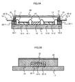
- FIG. 1 is a top view illustrating a semiconductor device according to a first embodiment of the present invention.
- FIG. 2A is a sectional view taken along a dotted and dashed line A-A' in FIG. 1 and
- FIG. 2B is a sectional view taken along a dotted and dashed line B-B' in FIG. 1 .
- FIG. 1 is a partially omitted illustration of the semiconductor device.
- GaAsFET 12 As illustrated in FIG. 1 , on a metal base substrate 11, GaAsFET 12, for example, is placed as a semiconductor element used for power amplification or the like. On input and output portions of the GaAsFET 12, there are placed a first dielectric substrate 13-1 and a second dielectric substrate 13-2 formed from, for example, ceramic.
- an input matching circuit 14-1 as a first circuit pattern is formed on the first dielectric substrate 13-1.
- an output matching circuit 14-2 as a second circuit pattern is formed on the second dielectric substrate 13-2.
- the input matching circuit 14-1 and the GaAsFET 12, and the GaAsFET 12 and an output matching circuit 14-2 are connected through a first connection portion, respectively.
- the first connection portion is composed of, for example, a plurality of first gold wires 15, each of which is a conductor line.
- the input matching circuit 14-1 is connected with a wire connection portion 24 which is one end of an input line 16-1 as a first waveguide through a second connection portion.
- the output matching circuit 14-2 is connected with a wire connection portion 24 which is one end of an output line 16-2 as a second waveguide through a second connection portion.
- the second connection portions are composed of a plurality of second gold wires 17, respectively.
- a lead connection portion 25 which is the other end of the input line 16-1 is connected with an input lead 18-1 connected to an external circuit (not illustrated).
- a lead connection portion 25 which is the other end of the output line 16-2 is connected with an output lead 18-2 connected to an external circuit (not illustrated).
- the input line 16-1 and the output line 16-2 are, for example, strip lines or micro strip lines at least having a surface formed from Au.
- a metal frame body 19 so as to surround the first dielectric substrate 13-1 having the input matching circuit 14-1, the GaAsFET 12 and the second dielectric substrate 13-2 having the output matching circuit 14-2.
- a metal lid 20 is disposed on the frame body 19.
- the inside of the device is sealed by the lid 20 and the frame body 19.
- the metal frame body 19 has recessed portions 21 at positions of the side portions opposed to each other.
- a first dielectric block 22-1 formed from, for example, ceramic is formed so as to stick out inwardly and outwardly beyond the frame body 19.
- the input line 16-1 or the output line 16-2 is formed on a surface of the first dielectric block 22-1.
- the input line 16-1 and the output line 16-2 are formed in a manner that a line width at the wire connection portions 24 is larger than that at the lead connection portions 25 connected to the input and output leads 18-1, 18-2, respectively.
- the line width at the wire connection portion 24 may be any large width, provided that the input line 16-1 or the output line 16-2 is in no contact with the metal frame body 19.
- the line width of the wire connection portion 24 may be any large width, provided that the input line 16-1 or the output line 16-2 is in no contact with the metal plating layer.
- a second dielectric block 22-2 made of a dielectric such as ceramic.
- the input and output lines 16-1, 16-2 are formed in a manner that a line width at the wire connection portions 24 is larger than that at the lead connection portions 25. Accordingly, the number of the second gold wires 17 composing the second connection portion can be increased.
- the number of the second gold wires 17 can be increased in this way, it is possible to increase the maximum allowable electric power at the second connection portion. Accordingly, in the semiconductor device according the embodiment of the present invention, high power output can be attained.
- the number of the second gold wires 17 can be increased, it is possible to further reduce a minimum impedance of the second connection portion. In other words, controlling the impedance of the second connection portion can be facilitated.
- controlling the impedance of the second connection portion is facilitated, thereby improving design flexibility of the input and output matching circuits 14-1, 14-2 connected with the second connection portions. Accordingly, more efficient input and output matching circuits 14-1, 14-2 can be designed.
- a first modified example illustrated in FIG. 3A is an example in which a line 161 of a line width equal to a line width at the wire connection portion 24 is formed from the inside to the outside of the frame body 19.
- a second modified example illustrated in FIG. 3B is an example in which a line 162 of a line width at the lead connection portion 25 is formed from the outside to the inside of the frame body 19.
- a third modified example illustrated in FIG. 3C is an example in which a line 163 is formed so that a line width becomes wider like a staircase pattern from the lead connection portion 25 toward the wire connection portion 24.
- a fourth modified example illustrated in FIG. 3D is an example in which a line 164 is formed so that a line width becomes wider in a tapered pattern from the lead connection portion 25 toward the wire connection portion 24.
- a fifth modified example illustrated in FIG. 3E is an example in which the wire connection portion 24 is formed in a comb-like pattern.
- the fifth modified example may be applied not only to the input and output lines 16-1, 16-2 illustrated in FIG. 1 but also to the input and output lines 16-1, 16-2 illustrated in FIGS. 3A to 3D .
- the number of the second gold wires 17 composing the second connection portion can be increased. Therefore, it is possible to increase the maximum allowable electric power at the second connection portion.
- the minimum impedance of the second connection portion can be further reduced, thereby allowing more efficient input and output matching circuits 14-1, 14-2 to be designed.
- FIG. 4A is a top view illustrating the semiconductor device according to the second embodiment and is an enlarged view of an area C in Fig. 1 .
- FIG. 4B is a sectional view taken along a dotted and dashed line D-D' in FIG. 4A .
- metal plating layers 42A, 42B composed of, for example, gold are formed on both side faces of the first dielectric block 22-1.
- protection patterns 41 A, 41 B composed of conductor such as the same material as the input and output lines 16-1, 16-2.
- the protection patterns 41 A, 41 B are provided for the following reason:
- metal plating composed of, for example, Au is formed on a surface of the first dielectric block 22-1 to stick out therebeyond.
- the amount of sticking-out metal is difficult to control in plating, which makes a sticking-out width vary among different positions.
- a sticking-out width of metal plating varies in this way, a distance between a sticking-out portion and the input and output lines 16-1, 16-2 becomes smaller and therefore the impedance of the input and output lines 16-1, 16-2 substantially changes with the sticking-out amount of metal plating.
- the semiconductor device has protection patterns 41A, 41 B on the first dielectric block 22-1 to prevent impedances of the input and output lines 16-1, 16-2 from being substantially changed due to a difference in the sticking-out width of metal plating.
- the protection patterns 41 A and 41 B provided in this way are provided so as to be in no contact with the input line 16-1 or the output line 16-2.
- the line width at the wire connection portion 24 may be any large width, provided that the input line 16-1 or the output line 16-2 is in no contact with the protection patterns 41A, 41 B.
- the protection patterns 41A, 41B are provided separately from the input and output lines 16-1, 16-2 along sides E1, E2 in no contact with the input line 16-1 nor the output line 16-2 of the first dielectric block 22-1.
- the protection patterns 41A, 41 B are provided so as to be spaced from the input and output lines 16-1, 16-2 along the input and output lines 16-1, 16-2.
- the protection patterns 41A, 41 B are provided so as to be spaced from the input and output lines 16-1, 16-2, at least, to such a degree as to be connected with metal plating layers 42A, 42B. This is because, in the case of no connection with the metal plating layers 42A, 42B, a signal running through the input line 16-1 or the output line 16-2 oscillates between the input line 16-1 or the output line 16-2 and the protection patterns 41A, 41 B.
- protection patterns 41A and 41 B are provided such that lengths thereof are equal to those of the sides E1 and E2.
- the sides E1, E2 are the ones formed by a face having the metal plating layers 42A, 42B thereon, of side faces of the first dielectric block 22-1 and a top face of the first dielectric block 22-1.
- a pattern width W1 of the protection pattern 41A and a pattern width W2 of the protection pattern 41 B are larger than a sticking-out width L1 of the metal plating layer 42A and a sticking-out width L2 of the metal plating layer 42B on the side faces of the first dielectric block 22-1.
- the pattern width W1 of the protection pattern 41 A and the pattern width W2 of the protection pattern 41 B are formed to be equal to each other.
- the sticking-out width L1 of the metal plating layer 42A and the sticking-out width L2 of the metal plating layer 42B on the side faces of the first dielectric block 22-1 are not always equal to each other.
- a width S1 between the protection pattern 41A and the input line 16-1 (or a width S1 between the protection pattern 41A and the output line 16-2) and a width S2 between the protection pattern 41 B and the input line 16-1 (or a width S2 between the protection pattern 41 B and the output line 16-2) are equal to each other.
- the number of the second gold wires 17 connected with the input and output lines 16-1, 16-2 can be increased. Further, since the distance between the input line 16-1 and the protection patterns 41 A, 41B and the distance between the output line 16-2 and the protection patterns 41A, 41 B can be kept constant, the impedances of the input and output lines 16-1, 16-2 can be easily controlled to be constant. Hence, the impedances of the input and output matching circuits 14-1, 14-2 and the impedances of the input and output lines 16-1, 16-2 can be sufficiently matched, respectively.
- the pattern width W1 of the protection pattern 41 A and the pattern width W2 of the protection pattern 41 B are not necessarily equal to each other.
- the width S1 between the protection pattern 41A and the input line 16-1 (or the width S1 between the protection pattern 41A and the output line 16-2) and the width S2 between the protection pattern 41 B and the input line 16-1 (the width S2 between the protection pattern 41 B and the output line 16-2) are not necessarily equal to each other.
- the width S1 between the protection patterns 41A and the input line 16-1 or the output line 16-2 may be made equal to the width S2 between the protection pattern 41 B and the input line 16-1 or the output line 16-2 by changing the pattern width W1 of the protection pattern 41A and the pattern width W2 of the protection pattern 41 B.
- the protection patterns 41A, 41 B are provided to have an equal length along the sides E1, E2.
- the protection patterns 41A, 41 B are not limited to the above-described embodiment.
- the protection patterns 41 A, 41 B may be formed as modified examples illustrated in FIGS. 5A to 5C .
- a first modified example illustrated in FIG. 5A is an example where protection walls 43 are provided on surfaces of the protection patterns 41A and 41 B.
- the protection walls 43 are formed on the sides of the input and output lines 16-1, 16-2 on the protection patterns 41A, 41 B.
- the protection walls 43 are formed to the protection patterns 41A, 41 B with the same length as the protection patterns 41A, 41 B on the protection patterns 41A, 41 B in parallel.
- the width of the protection wall 43 is not limited.
- the height is not limited, either, provided that the height is large enough to block sticking-out of the metal plating layer.
- a material of the protection wall 43 may be a conductor or a dielectric.
- a second modified example illustrated in FIG. 5B is an example where the protection patterns 41A, 41 B are provided to be spaced from the sides E1, E2.
- the spacing width is not limited, provided that sticking-out of the metal plating layers 42A, 42B connects the metal plating layers 42A, 42B and the protection patterns 41 A, 41 B, respectively.
- a third modified example illustrated in FIG. 5C is an example where protection patterns 46A, 46B are provided only along the wire connection portion 24.
- the impedance of only the wire connection portion 24 can be controlled. This is effective when a distance between the lead connection portion 25 and the sticking-out portions of the metal plating layers 42A, 42B is large enough for the impedances of the input and output lines 16-1, 16-2 to make no substantial changes.
- provision of the protection patterns 41A, 41 B, 46A, 46B allows distances between the protection patterns 41A, 41B, 46A, 46B and the input line 16-1 or the output line 16-2 to be equal to each other, respectively. Thereby it is possible to control easily so that the impedances of the input and output lines 16-1, 16-2 may steady.
- the impedance of the input line 16-1 or the output line 16-2 can be controlled by suitably forming the protection patterns 41A, 41 B, 46A, 46B described above in accordance with these geometries.
- the protection pattern may be provided along the geometry of the input line 16-1 or the output line 16-2.
- the protection patterns 46A, 46B each having a fixed small width
- protection patterns 45A, 45B each having a larger width than those of the protection patterns 46A, 46B
- the protection patterns 47A, 47B each having a width changing according to the tapered part
- protection patterns 45A, 46A, 47A, 45B, 46B, 47B are provided along a geometry of the input line 16-2 or the output line 16-2, sticking-out of the metal plating layers 42A, 42B beyond the protection patterns 45A, 46A, 47A, 45B, 46B, 47B can be restrained.
- the semiconductor device according to embodiments of the present invention has been described above. However, the semiconductor device according to embodiments of the present invention is not limited to the respective embodiments described above.
- connection between the input line 16-1 and the input matching circuit 14-1 or between the output matching circuit 14-2 and the output line 16-2 is not limited to the plurality of second wires 17, and may also be made through foil metal composed of gold foil 26, for example.
- Metal used for the first wire 15, the second wire 17 and the foil may be aluminum.
- a semiconductor element included in the semiconductor device according to embodiments of the present invention is not limited to GaAsFET 12, and may be GaNFET or any other semiconductor element. Further, the number of semiconductor elements is not limited to the number in the semiconductor device according to embodiments of the present invention described above.
- first and second dielectric substrates 13-1, 13-2 and the first and second dielectric blocks 22-1, 22-2 are not limited to ceramic.
- circuit patterns on the first dielectric substrate 13-1 and the second dielectric substrate 13-2 are not limited to the input and output matching circuits 14-1, 14-2.
Landscapes
- Engineering & Computer Science (AREA)
- Power Engineering (AREA)
- Microwave Amplifiers (AREA)
Abstract
A semiconductor device having a GaAsFET (12) and input (14.1) and output (14.2) matching circuits connected to the FET is provided. In the semiconductor device, a line, including a wire connection portion (24) connected to the input or output matching circuit and a lead connection portion (25) connected to an input or output lead which is connected to an external circuit, is formed in such a manner that a line width at the wire connection portion is wider than that at the lead connection portion. With the semiconductor device, the number of wires (17) connecting the input or output matching circuits with the wire connection portion (24) can be increased.
Description
- This application is based upon and claims the benefit of priority from the prior Japanese Patent Application No.
2008-284354 - The present invention relates to a semiconductor device with high design flexibility and capable of high power output.
- In a conventional semiconductor device, a semiconductor chip, input and output matching circuits are placed on a base substrate. That is, the semiconductor chip and the input and output matching circuits are placed in a metal frame body formed on the base substrate. In addition, a lid is placed on the frame body to seal the inside of the frame body.
- In such a semiconductor device, the semiconductor chip is connected to the input and output matching circuits formed on input and output sides, respectively, through a plurality of wires.
- Each of the input and output matching circuits is connected to an input or output line connected with either of an input lead or an output lead through a connection portion composed of a plurality of wires.
- Each of the input and output lines connected to the input and output matching circuits, respectively, is formed in a manner that one end thereof connected with the input or output lead has the same width as that of the other end thereof connected with the plurality of wires, as disclosed in Japanese Patent Application Laid-Open Nos.
2003-115732 2007-81125 - In the conventional semiconductor device, when a large amount of power is output, the output power may exceed an allowable electric power at the connection portion connecting the input or output line and the input or output matching circuit. In this case, there is posed a problem that wires composing the connection portion may melt.
- This melting of wires is resolved by increasing the number of wires composing the connection portion. This is because increasing the number of wires can increase the allowable electric power at the connection portion.
- However, in the conventional semiconductor device, the number of wires composing the connection portion is limited by a width of a line. Accordingly, the conventional semiconductor device has various electrical problems.
- A first problem is that the electric power which the semiconductor device can output is limited because limitation in the number of wires restricts the maximum allowable electric power at the connection portion.
- A second problem is that impedance matching between the connection portion and the input and output matching circuits is difficult because limitation in the number of wires restricts the minimum impedance of the connection portion. Accordingly, the conventional semiconductor device has a problem that flexibility in a circuit design of the input and output matching circuits is limited due to an impedance of the connection portion.
- It is therefore an object of the present invention to provide a semiconductor device having an increased number of wires composing a connection portion connecting input and output matching circuits with input and output lines.
- According to an embodiment of the present invention, there is provided a semiconductor device including: a base substrate; a semiconductor chip mounted on the base substrate; a dielectric substrate mounted on the base substrate; a circuit pattern mounted on the dielectric substrate and connected with the semiconductor chip through a conductor line; a dielectric block mounted on the base substrate; and a waveguide mounted on the dielectric block, the waveguide having a lead connection portion connected with an external device through a lead wire and a wire connection portion connected with the circuit pattern and having a larger width than the lead connection portion.
- According to another embodiment of the present invention, there is provided a semiconductor device including: a base substrate; a semiconductor chip mounted on the base substrate; a dielectric substrate mounted on the base substrate; a circuit pattern mounted on the dielectric substrate and connected with the semiconductor chip through a conductor line; a dielectric block mounted on the base substrate; a waveguide mounted on the dielectric block, the waveguide having a lead connection portion connected with an external device through a lead wire and a wire connection portion connected with the circuit pattern and having a larger width than the lead connection portion; a metal plating layer formed on a side face of the dielectric block; and a protection pattern formed from a conductor on the dielectric block in a manner spaced from the waveguide and connected to the metal plating layer and having a larger width than a sticking-out width of the metal plating layer.
-
-
FIG. 1 is a top view illustrating a semiconductor device according to a first embodiment of the present invention; -
FIG. 2A is a sectional view of the semiconductor device taken along a dotted and dashed line A-A' inFIG. 1 ; -
FIG. 2B is a sectional view of the semiconductor device taken along a dotted and dashed line B-B' inFIG. 1 ; -
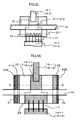
FIG. 3A is an enlarged view illustrating a first modified example of input and output lines formed on the semiconductor device according to the first embodiment; -
FIG. 3B is an enlarged view illustrating a second modified example of input and output lines formed on the semiconductor device according to the first embodiment; -
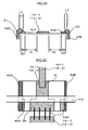
FIG. 3C is an enlarged view illustrating a third modified example of input and output lines formed on the semiconductor device according to the first embodiment; -
FIG. 3D is an enlarged view illustrating a fourth modified example of input and output lines formed on the semiconductor device according to the first embodiment; -
FIG. 3E is an enlarged view illustrating a fifth modified example of input and output lines formed on the semiconductor device according to the first embodiment; -
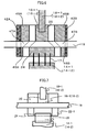
FIG. 4A is a top view illustrating a semiconductor device according to a second embodiment of the present invention and is an enlarged view of an area C inFig. 1 ; -
FIG. 4B is a sectional view of the semiconductor device taken along a dotted and dashed line D-D' inFIG. 4A ; -
FIG. 5A is a sectional view illustrating a first modified example of protection patterns formed on the semiconductor device according to the second embodiment of the present invention; -
FIG. 5B is a sectional view illustrating a second modified example of protection patterns formed on the semiconductor device according to the second embodiment of the present invention; -
FIG. 5C is an enlarged view illustrating a third modified example of protection patterns formed on the semiconductor device according to the second embodiment of the present invention; -
FIG. 6 is an enlarged view illustrating an applied example of protection patterns formed on the semiconductor device according to the second embodiment of the present invention; and -
FIG. 7 is an enlarged view illustrating another embodiment of a connection portion of the input and output lines with the input and output matching circuits of the semiconductor device according to the first and second embodiments of the present invention. - A semiconductor device according to an embodiment of the present invention will be described in detail with reference to the accompanying drawings.
-
FIG. 1 is a top view illustrating a semiconductor device according to a first embodiment of the present invention.FIG. 2A is a sectional view taken along a dotted and dashed line A-A' inFIG. 1 andFIG. 2B is a sectional view taken along a dotted and dashed line B-B' inFIG. 1 . However,FIG. 1 is a partially omitted illustration of the semiconductor device. - As illustrated in
FIG. 1 , on ametal base substrate 11, GaAsFET 12, for example, is placed as a semiconductor element used for power amplification or the like. On input and output portions of the GaAsFET 12, there are placed a first dielectric substrate 13-1 and a second dielectric substrate 13-2 formed from, for example, ceramic. - On the first dielectric substrate 13-1, an input matching circuit 14-1 as a first circuit pattern is formed. On the second dielectric substrate 13-2, an output matching circuit 14-2 as a second circuit pattern is formed.
- The input matching circuit 14-1 and the
GaAsFET 12, and the GaAsFET 12 and an output matching circuit 14-2 are connected through a first connection portion, respectively. The first connection portion is composed of, for example, a plurality offirst gold wires 15, each of which is a conductor line. - The input matching circuit 14-1 is connected with a
wire connection portion 24 which is one end of an input line 16-1 as a first waveguide through a second connection portion. Similarly, the output matching circuit 14-2 is connected with awire connection portion 24 which is one end of an output line 16-2 as a second waveguide through a second connection portion. The second connection portions are composed of a plurality ofsecond gold wires 17, respectively. - A
lead connection portion 25 which is the other end of the input line 16-1 is connected with an input lead 18-1 connected to an external circuit (not illustrated). Alead connection portion 25 which is the other end of the output line 16-2 is connected with an output lead 18-2 connected to an external circuit (not illustrated). - The input line 16-1 and the output line 16-2 are, for example, strip lines or micro strip lines at least having a surface formed from Au.
- On the
base substrate 11, there is formed ametal frame body 19 so as to surround the first dielectric substrate 13-1 having the input matching circuit 14-1, theGaAsFET 12 and the second dielectric substrate 13-2 having the output matching circuit 14-2. - As illustrated in
FIG. 2A , on theframe body 19, ametal lid 20 is disposed. The inside of the device is sealed by thelid 20 and theframe body 19. - As illustrated in
FIG. 2B , themetal frame body 19 has recessedportions 21 at positions of the side portions opposed to each other. In each of the recessedportions 21, a first dielectric block 22-1 formed from, for example, ceramic is formed so as to stick out inwardly and outwardly beyond theframe body 19. - On a surface of the first dielectric block 22-1, the input line 16-1 or the output line 16-2 is formed. The input line 16-1 and the output line 16-2 are formed in a manner that a line width at the
wire connection portions 24 is larger than that at thelead connection portions 25 connected to the input and output leads 18-1, 18-2, respectively. The line width at thewire connection portion 24 may be any large width, provided that the input line 16-1 or the output line 16-2 is in no contact with themetal frame body 19. - In a case where a metal plating layer is formed on a side face of the first dielectric block 22-1, the line width of the
wire connection portion 24 may be any large width, provided that the input line 16-1 or the output line 16-2 is in no contact with the metal plating layer. - On each of the input and output lines 16-1, 16-2, there is formed a second dielectric block 22-2 made of a dielectric such as ceramic.
- As described above, in the semiconductor device according to the present embodiment, the input and output lines 16-1, 16-2 are formed in a manner that a line width at the
wire connection portions 24 is larger than that at thelead connection portions 25. Accordingly, the number of thesecond gold wires 17 composing the second connection portion can be increased. - Since the number of the
second gold wires 17 can be increased in this way, it is possible to increase the maximum allowable electric power at the second connection portion. Accordingly, in the semiconductor device according the embodiment of the present invention, high power output can be attained. - Further, since the number of the
second gold wires 17 can be increased, it is possible to further reduce a minimum impedance of the second connection portion. In other words, controlling the impedance of the second connection portion can be facilitated. - Particularly in a high-frequency circuit, controlling the impedance of the second connection portion is facilitated, thereby improving design flexibility of the input and output matching circuits 14-1, 14-2 connected with the second connection portions. Accordingly, more efficient input and output matching circuits 14-1, 14-2 can be designed.
- Referring next to
FIGS. 3A to 3E , modified examples of the input and output lines 16-1, 16-2 will be described below. - A first modified example illustrated in
FIG. 3A is an example in which aline 161 of a line width equal to a line width at thewire connection portion 24 is formed from the inside to the outside of theframe body 19. - On the contrary, a second modified example illustrated in
FIG. 3B is an example in which aline 162 of a line width at thelead connection portion 25 is formed from the outside to the inside of theframe body 19. - A third modified example illustrated in
FIG. 3C is an example in which aline 163 is formed so that a line width becomes wider like a staircase pattern from thelead connection portion 25 toward thewire connection portion 24. - A fourth modified example illustrated in
FIG. 3D is an example in which aline 164 is formed so that a line width becomes wider in a tapered pattern from thelead connection portion 25 toward thewire connection portion 24. - Further, a fifth modified example illustrated in
FIG. 3E is an example in which thewire connection portion 24 is formed in a comb-like pattern. The fifth modified example may be applied not only to the input and output lines 16-1, 16-2 illustrated inFIG. 1 but also to the input and output lines 16-1, 16-2 illustrated inFIGS. 3A to 3D . - As illustrated in
FIGS. 3A to 3E , in the input and output lines 16-1, 16-2, it is sufficient that at least the line width at thewire connection portion 24 is larger than that at thelead connection portion 25. - Even in the semiconductor device having the input and output lines 16-1, 16-2 of the respective geometries described above, the number of the
second gold wires 17 composing the second connection portion can be increased. Therefore, it is possible to increase the maximum allowable electric power at the second connection portion. In addition, the minimum impedance of the second connection portion can be further reduced, thereby allowing more efficient input and output matching circuits 14-1, 14-2 to be designed. - Next, a semiconductor device according to a second embodiment of the present invention will be described below. The following description will be made only on a difference from the semiconductor device according to the first embodiment.
-
FIG. 4A is a top view illustrating the semiconductor device according to the second embodiment and is an enlarged view of an area C inFig. 1 .FIG. 4B is a sectional view taken along a dotted and dashed line D-D' inFIG. 4A . - As illustrated in
FIG. 4B , in the semiconductor device according to the present embodiment, metal plating layers 42A, 42B composed of, for example, gold are formed on both side faces of the first dielectric block 22-1. - As illustrated in
FIG. 4A , on the first dielectric block 22-1, there are formedprotection patterns protection patterns - In forming the metal plating layers 42A, 42B on the both side faces of the first dielectric block 22-1, metal plating composed of, for example, Au is formed on a surface of the first dielectric block 22-1 to stick out therebeyond. The amount of sticking-out metal is difficult to control in plating, which makes a sticking-out width vary among different positions. When a sticking-out width of metal plating varies in this way, a distance between a sticking-out portion and the input and output lines 16-1, 16-2 becomes smaller and therefore the impedance of the input and output lines 16-1, 16-2 substantially changes with the sticking-out amount of metal plating. Accordingly, there has been a problem that the impedance of the input matching circuit 14-1 connected through the second connection portion does not sufficiently match with the impedance of the input line 16-1. This is the same for impedance matching of the output matching circuit 14-2 with the output line 16-2.
- In view of the above, the semiconductor device according to the second embodiment of the present invention has
protection patterns - The
protection patterns wire connection portion 24 may be any large width, provided that the input line 16-1 or the output line 16-2 is in no contact with theprotection patterns - Concretely, the
protection patterns protection patterns - In this case, the
protection patterns protection patterns - Further, the
protection patterns - The sides E1, E2 are the ones formed by a face having the metal plating layers 42A, 42B thereon, of side faces of the first dielectric block 22-1 and a top face of the first dielectric block 22-1.
- As illustrated in
FIG. 4B , a pattern width W1 of theprotection pattern 41A and a pattern width W2 of theprotection pattern 41 B are larger than a sticking-out width L1 of themetal plating layer 42A and a sticking-out width L2 of themetal plating layer 42B on the side faces of the first dielectric block 22-1. However, the pattern width W1 of theprotection pattern 41 A and the pattern width W2 of theprotection pattern 41 B are formed to be equal to each other. - As illustrated in
FIG. 4B , the sticking-out width L1 of themetal plating layer 42A and the sticking-out width L2 of themetal plating layer 42B on the side faces of the first dielectric block 22-1 are not always equal to each other. - A width S1 between the
protection pattern 41A and the input line 16-1 (or a width S1 between theprotection pattern 41A and the output line 16-2) and a width S2 between theprotection pattern 41 B and the input line 16-1 (or a width S2 between theprotection pattern 41 B and the output line 16-2) are equal to each other. - According to the semiconductor device of the second embodiment described above, the number of the
second gold wires 17 connected with the input and output lines 16-1, 16-2 can be increased. Further, since the distance between the input line 16-1 and theprotection patterns protection patterns - Unlike the
protection patterns FIG. 4B , the pattern width W1 of theprotection pattern 41 A and the pattern width W2 of theprotection pattern 41 B are not necessarily equal to each other. - The width S1 between the
protection pattern 41A and the input line 16-1 (or the width S1 between theprotection pattern 41A and the output line 16-2) and the width S2 between theprotection pattern 41 B and the input line 16-1 (the width S2 between theprotection pattern 41 B and the output line 16-2) are not necessarily equal to each other. - When the input line 16-1 or the output line 16-2 is not in the center of the first dielectric block 22-1, the width S1 between the
protection patterns 41A and the input line 16-1 or the output line 16-2 may be made equal to the width S2 between theprotection pattern 41 B and the input line 16-1 or the output line 16-2 by changing the pattern width W1 of theprotection pattern 41A and the pattern width W2 of theprotection pattern 41 B. - In the above embodiment, the
protection patterns protection patterns protection patterns FIGS. 5A to 5C . - A first modified example illustrated in
FIG. 5A is an example whereprotection walls 43 are provided on surfaces of theprotection patterns 41A and 41 B. Preferably, theprotection walls 43 are formed on the sides of the input and output lines 16-1, 16-2 on theprotection patterns 41A, 41 B. In addition, preferably, theprotection walls 43 are formed to theprotection patterns protection patterns protection patterns - The width of the
protection wall 43 is not limited. The height is not limited, either, provided that the height is large enough to block sticking-out of the metal plating layer. - A material of the
protection wall 43 may be a conductor or a dielectric. - As described above, by forming the
protection walls 43 on theprotection patterns protection patterns - A second modified example illustrated in
FIG. 5B is an example where theprotection patterns protection patterns - A third modified example illustrated in
FIG. 5C is an example whereprotection patterns wire connection portion 24. In this case, the impedance of only thewire connection portion 24 can be controlled. This is effective when a distance between thelead connection portion 25 and the sticking-out portions of the metal plating layers 42A, 42B is large enough for the impedances of the input and output lines 16-1, 16-2 to make no substantial changes. - As described above, provision of the
protection patterns protection patterns - Even when a geometry of the input line 16-1 or the output line 16-2 is as illustrated in any of
FIGS. 3A to 3E , the impedance of the input line 16-1 or the output line 16-2 can be controlled by suitably forming theprotection patterns - For example, as illustrated in
FIG. 6 , when the input line 16-1 or the output line 16-2 is formed to become wider in a tapered manner from thelead connection portion 25 having a fixed width toward thewire connection portion 24 having a fixed width, the protection pattern may be provided along the geometry of the input line 16-1 or the output line 16-2. - Concretely, at portions along the
wire connection portion 24, theprotection patterns lead connection portion 25,protection patterns protection patterns protection patterns - As described above, even when the
protection patterns protection patterns - The semiconductor device according to embodiments of the present invention has been described above. However, the semiconductor device according to embodiments of the present invention is not limited to the respective embodiments described above.
- For example, as illustrated in
FIG. 7 , the connection between the input line 16-1 and the input matching circuit 14-1 or between the output matching circuit 14-2 and the output line 16-2 is not limited to the plurality ofsecond wires 17, and may also be made through foil metal composed ofgold foil 26, for example. Metal used for thefirst wire 15, thesecond wire 17 and the foil may be aluminum. - A semiconductor element included in the semiconductor device according to embodiments of the present invention is not limited to
GaAsFET 12, and may be GaNFET or any other semiconductor element. Further, the number of semiconductor elements is not limited to the number in the semiconductor device according to embodiments of the present invention described above. - In addition, the first and second dielectric substrates 13-1, 13-2 and the first and second dielectric blocks 22-1, 22-2 are not limited to ceramic. Further, circuit patterns on the first dielectric substrate 13-1 and the second dielectric substrate 13-2 are not limited to the input and output matching circuits 14-1, 14-2.
Claims (13)
- A semiconductor device comprising:a base substrate;a semiconductor chip mounted on the base substrate;a dielectric substrate mounted on the base substrate;a circuit pattern mounted on the dielectric substrate and connected with the semiconductor chip through a conductor line;a dielectric block mounted on the base substrate; anda waveguide mounted on the dielectric block, the waveguide having a lead connection portion connected with an external device through a lead wire and a wire connection portion connected with the circuit pattern and having a larger width than the lead connection portion.
- A semiconductor device comprising:a base substrate;a semiconductor chip mounted on the base substrate;a dielectric substrate mounted on the base substrate;a circuit pattern mounted on the dielectric substrate and connected with the semiconductor chip through a conductor line;a dielectric block mounted on the base substrate;a waveguide mounted on the dielectric block, the waveguide having a lead connection portion connected with an external device through a lead wire and a wire connection portion connected with the circuit pattern and having a larger width than the lead connection portion;a metal plating layer formed on a side face of the dielectric block; anda protection pattern formed from a conductor on the dielectric block in a manner spaced from the waveguide and connected to the metal plating layer and having a larger width than a sticking-out width of the metal plating layer.
- The semiconductor device according to claim 2, wherein
the protection pattern has a protection wall on a surface of the protection pattern for blocking sticking-out of the metal plating layer, and
the protection wall is spaced from the waveguide and has a height large enough to block sticking-out of the metal plating layer. - The semiconductor device according to either of claims 2 or 3, wherein the protection pattern is provided at an interval relative to a side formed by a surface of the dielectric block and a surface on which a metal plating layer is provided.
- The semiconductor device according to either of claims 2 or 3, wherein the protection pattern is provided at a fixed interval relative to the waveguide.
- The semiconductor device according to any preceding claim, wherein the wire connection portion is formed like a comb-like pattern.
- The semiconductor device according to any preceding claim, wherein the waveguide becomes wider in a tapered manner from the lead connection portion toward the wire connection portion.
- The semiconductor device according to any of claims 1 to 6, wherein the waveguide becomes wider in a staircase pattern from the lead connection portion toward the wire connection portion.
- The semiconductor device according to any preceding claim, wherein the conductor line is composed of wires.
- The semiconductor device according to claim 9, wherein wires are formed from gold, respectively.
- The semiconductor device according to any preceding claim, wherein the circuit pattern is connected with the wire connection portion through a metal foil.
- The semiconductor device according to claim 11, wherein the metal foil is formed from gold.
- The semiconductor device according to any preceding claim, wherein the circuit pattern is a matching circuit.
Applications Claiming Priority (1)
| Application Number | Priority Date | Filing Date | Title |
|---|---|---|---|
| JP2008284354 | 2008-11-05 |
Publications (1)
| Publication Number | Publication Date |
|---|---|
| EP2184778A1 true EP2184778A1 (en) | 2010-05-12 |
Family
ID=41630377
Family Applications (1)
| Application Number | Title | Priority Date | Filing Date |
|---|---|---|---|
| EP09251900A Withdrawn EP2184778A1 (en) | 2008-11-05 | 2009-07-29 | Semiconductor device |
Country Status (3)
| Country | Link |
|---|---|
| US (2) | US8102036B2 (en) |
| EP (1) | EP2184778A1 (en) |
| JP (1) | JP2010135722A (en) |
Cited By (1)
| Publication number | Priority date | Publication date | Assignee | Title |
|---|---|---|---|---|
| EP2234157A3 (en) * | 2009-03-23 | 2011-06-22 | Kabushiki Kaisha Toshiba | Semiconductor device |
Families Citing this family (11)
| Publication number | Priority date | Publication date | Assignee | Title |
|---|---|---|---|---|
| JP2010135722A (en) * | 2008-11-05 | 2010-06-17 | Toshiba Corp | Semiconductor device |
| US8471382B2 (en) * | 2010-11-18 | 2013-06-25 | Kabushiki Kaisha Toshiba | Package and high frequency terminal structure for the same |
| JP5439415B2 (en) * | 2011-03-01 | 2014-03-12 | 株式会社東芝 | Package for MMIC |
| GB201105912D0 (en) * | 2011-04-07 | 2011-05-18 | Diamond Microwave Devices Ltd | Improved matching techniques for power transistors |
| JP6012953B2 (en) * | 2011-11-16 | 2016-10-25 | 株式会社東芝 | High frequency semiconductor device |
| JP5892770B2 (en) * | 2011-11-16 | 2016-03-23 | 株式会社東芝 | High frequency semiconductor device |
| JP5951265B2 (en) * | 2012-01-26 | 2016-07-13 | 株式会社東芝 | Broadband amplifier |
| JP5851334B2 (en) * | 2012-05-08 | 2016-02-03 | 株式会社東芝 | High frequency semiconductor package |
| JP6273247B2 (en) * | 2015-12-03 | 2018-01-31 | 株式会社東芝 | High frequency semiconductor amplifier |
| CN110140205B (en) | 2016-12-29 | 2023-08-25 | 三菱电机株式会社 | Semiconductor device with a semiconductor device having a plurality of semiconductor chips |
| JP6866789B2 (en) * | 2017-07-11 | 2021-04-28 | 富士通株式会社 | Electronic devices and methods for manufacturing electronic devices |
Citations (9)
| Publication number | Priority date | Publication date | Assignee | Title |
|---|---|---|---|---|
| US4672151A (en) * | 1984-10-08 | 1987-06-09 | Fujitsu Limited | Package for a microwave semiconductor device |
| US5023993A (en) * | 1988-09-30 | 1991-06-18 | Grumman Aerospace Corporation | Method for manufacturing a high-performance package for monolithic microwave integrated circuits |
| WO1999040627A1 (en) * | 1998-01-26 | 1999-08-12 | Giga A/S | An electrical connecting element and a method of making such an element |
| US6023080A (en) * | 1997-02-12 | 2000-02-08 | Kabushiki Kaisha Toshiba | Input/output connection structure of a semiconductor device |
| US6043556A (en) * | 1997-02-27 | 2000-03-28 | Kyocera Corporation | High-frequency input/output feedthrough and package for housing high-frequency semiconductor element using same |
| JP2003115732A (en) | 2001-10-03 | 2003-04-18 | Hitachi Ltd | Semiconductor device |
| US20040174231A1 (en) * | 2001-05-11 | 2004-09-09 | Matsushita Electric Industrial Co., Ltd. | High-frequency semiconductor device |
| JP2007081125A (en) | 2005-09-14 | 2007-03-29 | Toshiba Corp | High frequency package |
| JP2008284354A (en) | 2007-05-21 | 2008-11-27 | Biospace Co Ltd | Biological impedance measuring apparatus |
Family Cites Families (15)
| Publication number | Priority date | Publication date | Assignee | Title |
|---|---|---|---|---|
| FR2538617B1 (en) * | 1982-12-28 | 1986-02-28 | Thomson Csf | ENCAPSULATION BOX FOR POWER SEMICONDUCTOR WITH IMPROVED INPUT-OUTPUT ISOLATION |
| JPH0770891B2 (en) * | 1987-08-11 | 1995-07-31 | 三菱電機株式会社 | Power distributor |
| JPH0775295B2 (en) * | 1989-08-04 | 1995-08-09 | 松下電器産業株式会社 | High frequency transistor matching circuit |
| JPH03297201A (en) * | 1990-04-16 | 1991-12-27 | Mitsubishi Electric Corp | High frequency semiconductor device |
| JPH05136607A (en) * | 1991-11-15 | 1993-06-01 | Toshiba Corp | Microwave transistor for power amplification |
| US6441697B1 (en) * | 1999-01-27 | 2002-08-27 | Kyocera America, Inc. | Ultra-low-loss feedthrough for microwave circuit package |
| FI106414B (en) * | 1999-02-02 | 2001-01-31 | Nokia Networks Oy | Bredbandsimpedansadapter |
| US6950565B2 (en) * | 2002-10-07 | 2005-09-27 | Agere Systems Inc | Submount for high speed electronic devices |
| JP2004200242A (en) * | 2002-12-16 | 2004-07-15 | Kyocera Corp | Package for storing semiconductor elements |
| JP4255801B2 (en) * | 2003-10-17 | 2009-04-15 | 三菱電機株式会社 | Power synthesis type high output FET |
| JP3944193B2 (en) * | 2004-02-09 | 2007-07-11 | 太陽誘電株式会社 | Balun and balance filter and wireless communication equipment |
| JP4455352B2 (en) * | 2005-01-24 | 2010-04-21 | 立山科学工業株式会社 | Manufacturing method of substrate for electronic device |
| JP2007189062A (en) * | 2006-01-13 | 2007-07-26 | Mitsubishi Electric Corp | HPA package |
| DE102008043156A1 (en) * | 2008-10-24 | 2010-05-06 | Kuka Roboter Gmbh | Mounting device, medical robot and method for adjusting the tool center point of a medical robot |
| JP2010135722A (en) * | 2008-11-05 | 2010-06-17 | Toshiba Corp | Semiconductor device |
-
2009
- 2009-03-23 JP JP2009070852A patent/JP2010135722A/en active Pending
- 2009-07-29 EP EP09251900A patent/EP2184778A1/en not_active Withdrawn
- 2009-07-29 US US12/511,492 patent/US8102036B2/en active Active
-
2010
- 2010-02-23 US US12/710,824 patent/US20100237486A1/en not_active Abandoned
Patent Citations (10)
| Publication number | Priority date | Publication date | Assignee | Title |
|---|---|---|---|---|
| US4672151A (en) * | 1984-10-08 | 1987-06-09 | Fujitsu Limited | Package for a microwave semiconductor device |
| US5023993A (en) * | 1988-09-30 | 1991-06-18 | Grumman Aerospace Corporation | Method for manufacturing a high-performance package for monolithic microwave integrated circuits |
| US6023080A (en) * | 1997-02-12 | 2000-02-08 | Kabushiki Kaisha Toshiba | Input/output connection structure of a semiconductor device |
| US6043556A (en) * | 1997-02-27 | 2000-03-28 | Kyocera Corporation | High-frequency input/output feedthrough and package for housing high-frequency semiconductor element using same |
| WO1999040627A1 (en) * | 1998-01-26 | 1999-08-12 | Giga A/S | An electrical connecting element and a method of making such an element |
| US20040174231A1 (en) * | 2001-05-11 | 2004-09-09 | Matsushita Electric Industrial Co., Ltd. | High-frequency semiconductor device |
| JP2003115732A (en) | 2001-10-03 | 2003-04-18 | Hitachi Ltd | Semiconductor device |
| JP2007081125A (en) | 2005-09-14 | 2007-03-29 | Toshiba Corp | High frequency package |
| EP1772904A2 (en) * | 2005-09-14 | 2007-04-11 | Kabushiki Kaisha Toshiba | Package for high frequency waves containing high frequency electronic circuit |
| JP2008284354A (en) | 2007-05-21 | 2008-11-27 | Biospace Co Ltd | Biological impedance measuring apparatus |
Cited By (1)
| Publication number | Priority date | Publication date | Assignee | Title |
|---|---|---|---|---|
| EP2234157A3 (en) * | 2009-03-23 | 2011-06-22 | Kabushiki Kaisha Toshiba | Semiconductor device |
Also Published As
| Publication number | Publication date |
|---|---|
| US20100237486A1 (en) | 2010-09-23 |
| US20100109165A1 (en) | 2010-05-06 |
| JP2010135722A (en) | 2010-06-17 |
| US8102036B2 (en) | 2012-01-24 |
Similar Documents
| Publication | Publication Date | Title |
|---|---|---|
| US8102036B2 (en) | Semiconductor device in which a semiconductor chip is sealed | |
| US20170358516A1 (en) | Power module | |
| US9620448B1 (en) | Power module | |
| US6555755B1 (en) | Flexible interconnecting substrate and method of manufacturing the same, film carrier, tape-shaped semiconductor device, semiconductor device, circuit board, and electronic equipment | |
| EP3113218B1 (en) | Package for an electronic-component and electronic device including the package | |
| CN103021967A (en) | Power semiconductor module with integrated thick-film printed circuit board | |
| EP3118895B1 (en) | Package for housing an electronic component and electronic device including the package | |
| EP3493252B1 (en) | Substrate for mounting semiconductor element and semiconductor device | |
| US7781899B2 (en) | Leadframe having mold lock vent | |
| TWI680555B (en) | Electronic module | |
| US7303113B2 (en) | Method and structure for controlled impedance wire bonds using co-dispensing of dielectric spacers | |
| CN110140205B (en) | Semiconductor device with a semiconductor device having a plurality of semiconductor chips | |
| US9386687B2 (en) | Electronic component housing package and electronic apparatus | |
| KR100715411B1 (en) | Hybrid integrated circuit device | |
| CN109511279B (en) | electronic module | |
| WO2020175626A1 (en) | Electronic-element mounting package and electronic device | |
| CN110622286A (en) | Amplifier with a high-frequency amplifier | |
| JP7658960B2 (en) | Semiconductor Device | |
| US12381135B2 (en) | Electronic package and electronic device comprising the same | |
| JP7666175B2 (en) | Semiconductor device and package | |
| CN100401510C (en) | Semiconductor device, semiconductor body and method for manufacturing the same | |
| JP2008112810A (en) | Circuit board, semiconductor element storage package, and semiconductor device | |
| EP2234157A2 (en) | Semiconductor device | |
| JP6022842B2 (en) | Semiconductor element storage package and semiconductor device | |
| JP5257763B2 (en) | Multilayer circuit board |
Legal Events
| Date | Code | Title | Description |
|---|---|---|---|
| PUAI | Public reference made under article 153(3) epc to a published international application that has entered the european phase |
Free format text: ORIGINAL CODE: 0009012 |
|
| 17P | Request for examination filed |
Effective date: 20090818 |
|
| AK | Designated contracting states |
Kind code of ref document: A1 Designated state(s): AT BE BG CH CY CZ DE DK EE ES FI FR GB GR HR HU IE IS IT LI LT LU LV MC MK MT NL NO PL PT RO SE SI SK SM TR |
|
| AX | Request for extension of the european patent |
Extension state: AL BA RS |
|
| 17Q | First examination report despatched |
Effective date: 20101129 |
|
| STAA | Information on the status of an ep patent application or granted ep patent |
Free format text: STATUS: THE APPLICATION IS DEEMED TO BE WITHDRAWN |
|
| 18D | Application deemed to be withdrawn |
Effective date: 20130201 |