EP2184635A1 - Rückbeleuchtungseinheit mit fest eingebautem Drahtgitter-Polarisator - Google Patents
Rückbeleuchtungseinheit mit fest eingebautem Drahtgitter-Polarisator Download PDFInfo
- Publication number
- EP2184635A1 EP2184635A1 EP09175695A EP09175695A EP2184635A1 EP 2184635 A1 EP2184635 A1 EP 2184635A1 EP 09175695 A EP09175695 A EP 09175695A EP 09175695 A EP09175695 A EP 09175695A EP 2184635 A1 EP2184635 A1 EP 2184635A1
- Authority
- EP
- European Patent Office
- Prior art keywords
- backlight unit
- wire grid
- substrate
- grid polarizer
- electron emission
- Prior art date
- Legal status (The legal status is an assumption and is not a legal conclusion. Google has not performed a legal analysis and makes no representation as to the accuracy of the status listed.)
- Withdrawn
Links
Images


Classifications
-
- G—PHYSICS
- G02—OPTICS
- G02F—OPTICAL DEVICES OR ARRANGEMENTS FOR THE CONTROL OF LIGHT BY MODIFICATION OF THE OPTICAL PROPERTIES OF THE MEDIA OF THE ELEMENTS INVOLVED THEREIN; NON-LINEAR OPTICS; FREQUENCY-CHANGING OF LIGHT; OPTICAL LOGIC ELEMENTS; OPTICAL ANALOGUE/DIGITAL CONVERTERS
- G02F1/00—Devices or arrangements for the control of the intensity, colour, phase, polarisation or direction of light arriving from an independent light source, e.g. switching, gating or modulating; Non-linear optics
- G02F1/01—Devices or arrangements for the control of the intensity, colour, phase, polarisation or direction of light arriving from an independent light source, e.g. switching, gating or modulating; Non-linear optics for the control of the intensity, phase, polarisation or colour
- G02F1/13—Devices or arrangements for the control of the intensity, colour, phase, polarisation or direction of light arriving from an independent light source, e.g. switching, gating or modulating; Non-linear optics for the control of the intensity, phase, polarisation or colour based on liquid crystals, e.g. single liquid crystal display cells
- G02F1/133—Constructional arrangements; Operation of liquid crystal cells; Circuit arrangements
- G02F1/1333—Constructional arrangements; Manufacturing methods
- G02F1/1335—Structural association of cells with optical devices, e.g. polarisers or reflectors
- G02F1/1336—Illuminating devices
- G02F1/13362—Illuminating devices providing polarized light, e.g. by converting a polarisation component into another one
-
- G—PHYSICS
- G02—OPTICS
- G02F—OPTICAL DEVICES OR ARRANGEMENTS FOR THE CONTROL OF LIGHT BY MODIFICATION OF THE OPTICAL PROPERTIES OF THE MEDIA OF THE ELEMENTS INVOLVED THEREIN; NON-LINEAR OPTICS; FREQUENCY-CHANGING OF LIGHT; OPTICAL LOGIC ELEMENTS; OPTICAL ANALOGUE/DIGITAL CONVERTERS
- G02F1/00—Devices or arrangements for the control of the intensity, colour, phase, polarisation or direction of light arriving from an independent light source, e.g. switching, gating or modulating; Non-linear optics
- G02F1/01—Devices or arrangements for the control of the intensity, colour, phase, polarisation or direction of light arriving from an independent light source, e.g. switching, gating or modulating; Non-linear optics for the control of the intensity, phase, polarisation or colour
- G02F1/13—Devices or arrangements for the control of the intensity, colour, phase, polarisation or direction of light arriving from an independent light source, e.g. switching, gating or modulating; Non-linear optics for the control of the intensity, phase, polarisation or colour based on liquid crystals, e.g. single liquid crystal display cells
- G02F1/133—Constructional arrangements; Operation of liquid crystal cells; Circuit arrangements
- G02F1/1333—Constructional arrangements; Manufacturing methods
- G02F1/1335—Structural association of cells with optical devices, e.g. polarisers or reflectors
-
- H—ELECTRICITY
- H01—ELECTRIC ELEMENTS
- H01J—ELECTRIC DISCHARGE TUBES OR DISCHARGE LAMPS
- H01J61/00—Gas-discharge or vapour-discharge lamps
- H01J61/02—Details
- H01J61/30—Vessels; Containers
- H01J61/305—Flat vessels or containers
-
- H—ELECTRICITY
- H01—ELECTRIC ELEMENTS
- H01J—ELECTRIC DISCHARGE TUBES OR DISCHARGE LAMPS
- H01J63/00—Cathode-ray or electron-stream lamps
- H01J63/06—Lamps with luminescent screen excited by the ray or stream
-
- G—PHYSICS
- G02—OPTICS
- G02F—OPTICAL DEVICES OR ARRANGEMENTS FOR THE CONTROL OF LIGHT BY MODIFICATION OF THE OPTICAL PROPERTIES OF THE MEDIA OF THE ELEMENTS INVOLVED THEREIN; NON-LINEAR OPTICS; FREQUENCY-CHANGING OF LIGHT; OPTICAL LOGIC ELEMENTS; OPTICAL ANALOGUE/DIGITAL CONVERTERS
- G02F1/00—Devices or arrangements for the control of the intensity, colour, phase, polarisation or direction of light arriving from an independent light source, e.g. switching, gating or modulating; Non-linear optics
- G02F1/01—Devices or arrangements for the control of the intensity, colour, phase, polarisation or direction of light arriving from an independent light source, e.g. switching, gating or modulating; Non-linear optics for the control of the intensity, phase, polarisation or colour
- G02F1/13—Devices or arrangements for the control of the intensity, colour, phase, polarisation or direction of light arriving from an independent light source, e.g. switching, gating or modulating; Non-linear optics for the control of the intensity, phase, polarisation or colour based on liquid crystals, e.g. single liquid crystal display cells
- G02F1/133—Constructional arrangements; Operation of liquid crystal cells; Circuit arrangements
- G02F1/1333—Constructional arrangements; Manufacturing methods
- G02F1/1335—Structural association of cells with optical devices, e.g. polarisers or reflectors
- G02F1/133528—Polarisers
- G02F1/133548—Wire-grid polarisers
-
- G—PHYSICS
- G02—OPTICS
- G02F—OPTICAL DEVICES OR ARRANGEMENTS FOR THE CONTROL OF LIGHT BY MODIFICATION OF THE OPTICAL PROPERTIES OF THE MEDIA OF THE ELEMENTS INVOLVED THEREIN; NON-LINEAR OPTICS; FREQUENCY-CHANGING OF LIGHT; OPTICAL LOGIC ELEMENTS; OPTICAL ANALOGUE/DIGITAL CONVERTERS
- G02F2202/00—Materials and properties
- G02F2202/22—Antistatic materials or arrangements
Definitions
- the present invention relates to a backlight unit, and more particularly, to a backlight unit having improved luminous efficiency.
- electron emission devices may be classified as either a type which uses a hot cathode as an electron emission source or a type which uses a cold cathode as an electron emission source.
- Field Emission Devices FEDs
- SCEs Surface Conduction Emitters
- MIMs Metal Insulator Metals
- MISs Metal Insulator Semiconductors
- BSEs Ballistic electron Surface Emitting types
- FED type electron emission devices are based on the principle that when a material having a low work function or a high beta function is used as an electron emission source, electrons are easily emitted in a vacuum due to an electric field difference.
- the following types of FED type electron emission devices have been developed: ones which employ a tapered tip structure formed of, for example, molybdenum (Mo) or silicon (Si) as a main component, ones which employ a carbonaceous material such as graphite or Diamond-Like Carbon (DLC), and ones which employ a nano material such as nanotubes or nanowires, as electron emission sources.
- FED type electron emission devices may be largely classified as either top gate type or under gate type, according to an arrangement of a cathode electrode and a gate electrode. FED type electron emission devices may also be classified as diode type, triode type, or tetrode type according to the total number of electrodes used.
- a conventional electron emission device electrons are emitted from an electron emission source due to an electric field formed between a cathode electrode and a gate electrode. That is, electrons are emitted from the electron emission source disposed around one of a cathode electrode and a gate electrode, which operates as a cathode. The emitted electrons travel toward the other of the cathode electrode and the gate electrode, which operates as an anode, in a beginning stage, and are then accelerated toward a phosphor layer due to a strong electric field of an anode electrode.
- a backlight unit which is a type of electron emission device, includes a polarizer.
- the polarizer is a type of device which obtains linear polarized light based on the principle that the color of transmitted polarized light varies according to the location of an optical isomer.
- the transmissivity of non-polarized light that is primarily incident on a polarizer is about 30 to 40 percent (%) and the remaining roughly 60 percent (%) of the non-polarized light is absorbed or reflected by the polarizer.
- Absorption or reflection of light by the polarizer is a main factor of degradation of luminous efficiency of a backlight.
- the wire grid polarizer is formed by performing line patterning on a conductor in order to divide the conductor into regions having dimensions similar to a wavelength of light of a region of interest, so that electric-field oscillating components that intersect a grid may pass through the grid, but the energy of electric-field oscillating components that are not correctly aligned with respect to the grid is partially absorbed or reflected by the grid.
- the wire grid polarizer has an advantage in that an optical reproducing efficiency is high since internal absorption is less than in a conventional polarizer, and the transmissivity of selectively transmitted polarized light and the rate of back reflection of non-selected polarized light are higher than in a conventional polarizer. In this case, conversion of polarized light, such as oval polarized light, should be performed in order to reuse light reflected in a rear surface.
- a diffusion sheet is disposed between an optical source and a wire grid polarizer, and thus, light reflected on a rear surface in an optical path passes through the diffusion sheet two or more times, thereby causing an optical loss.
- the wire grid polarizer is disposed between the optical source and the diffusion sheet, the wire grid polarizer and the optical source are installed to be separated from each other. Thus an optical loss occurs in a space between the wire grid polarizer and the optical source.
- an increase in the optical diffusion performance of the diffusion sheet results in a reduction in the transmissivity of light, and therefore, the diffusion sheet itself causes an optical loss.
- an electron emission type backlight unit since voltage is applied to an anode surface, static electricity is induced onto an external surface of a substrate.
- the induced static electricity is one of a number of factors that cause a device to operate unstably, and may cause unnecessary particles, such as dust, to stick to an external surface of the backlight unit.
- Exemplary embodiments of the present invention provide a backlight unit having improved luminous efficiency.
- a backlight unit for a non-emissive display device having an integral wire grid polarizer.
- FIG. 1 is a partial perspective view of an election emission type backlight unit 100 including an electron emission device 101 according to an embodiment of the present invention.
- FIG. 2 is a cross-sectional view of FIG. 1 taken along the line II-II.
- a diffusion sheet 190 and a liquid crystal display (LCD) panel 200 illustrated in FIG. 2 are not illustrated in FIG. 1 .
- LCD liquid crystal display
- the backlight unit 100 includes the electron emission device 101 and a front panel 102 that are aligned in parallel to form a light emitting space 103, which is a vacuum space, and spacers 160 disposed to maintain a distance between the electron emission device 101 and the front panel 102.
- the electron emission device 101 includes a first substrate 110, a plurality of first electrodes 120, an insulating layer 130, a plurality of second electrodes 140, and a plurality of electron emission sources 150.
- first electrodes 120 and the second electrodes 140 are arranged to cross one another on the first substrate 110.
- the insulating layer 130 is formed between the first and second electrodes 120 and 140 in order to electrically insulate the first and second electrodes 120 and 140 from each other.
- a plurality of electron emission holes 131 are respectively formed on locations where the first and second electrodes 120 and 140 cross each other.
- the electron emission sources 150 are respectively included in the electron emission holes 131.
- the first substrate 110 is a plate having a thickness (e.g., a predetermined thickness), and may be formed of quartz glass, glass containing an amount of impurities (e.g., Na), plate glass, a glass substrate coated with SiO2, or an aluminum oxide or ceramic substrate. In embodiments having a flexible display apparatus, the first substrate 110 may be formed of a flexible material.
- the first and second electrodes 120 and 140 may be formed of an electrically conductive material that is well known in the art.
- the first and second electrodes 120 and 140 may be formed of metals such as Al, Ti, Cr, Ni, Au, Ag, Mo, W, Pt, Cu, or Pd, or an alloy thereof.
- the first and second electrodes 120 and 140 may also be formed of a printed conductor including glass and a metal such as Pd, Ag, RuO 2 , or Pd-Ag, or a metal oxide thereof.
- the first and second electrodes 120 and 140 may also be formed of a transparent conductor such as In 2 O 3 or SnO 2 , or a semiconductor material such as polysilicon.
- the insulating layer 130 insulates the first and second electrodes 120 and 140.
- the insulating layer 130 may be formed of a general insulating layer.
- the insulating material may be a silicon oxide, a silicon nitride, frit, or a similar material.
- frit examples include, but are not limited to, PbO-SiO 2 -based frit, PbO-B 2 O 3 -SiO 2 -bascd frit, ZnO-SiO 2 -based frit, ZnO-B 2 O 3 -SiO 2 -based frit, Bi 2 O 3 -SiO 2 -based frit, and Bi 2 O 3 -B 2 O 3 -SiO 2 -based frit.
- the electron emission sources 150 contain an electron emission material.
- the electron emission material may be a carbon nanotube (CNT) that has a low work function and a high beta function.
- the carbon nanotube has good electron emission characteristics, thus enabling a low voltage operation.
- an apparatus using a carbon nanotube as an electron emission source may be easily manufactured on a large scale.
- the electron emission material is not limited to a carbon nanotube, and may be, for example, a carbonaceous material such as graphite, diamond, or diamond-like carbon, or a nano material such as nanotube, nanowire, or nanorod.
- the electron emission material may also include a carbide-derived carbon.
- the front panel 102 includes a second substrate 171 which may be transparent, a phosphor layer 175 which is disposed on the second substrate 171 and which is excited by electrons emitted from the electron emission device 101 for emitting visible light, a third electrode 173 which accelerates the electrons emitted from the electron emission device 101 toward the phosphor layer 175, and a wire grid polarizer 180.
- the second substrate 171 may be formed of the same material as the first substrate 110 and may be transparent.
- the third electrode 173 may be formed of the same material as the first or second electrodes 120 or 140. That is, the third electrode 173 may be formed of a metal such as Al, Ti, Cr, Ni, Au, Ag, Mo, W, Pt, Cu, or Pd, or an alloy thereof; a printed conductor including glass and a metal such as Pd, Ag, RuO 2 , or Pd-Ag or a metal oxide thereof; a transparent conductor such as In 2 O 3 or SnO 2 ; or a semiconductor material such as polysilicon.
- the third electrode 173 may be formed of an Al thin film. If the third electrode 173 is formed of an Al thin film, accelerated electrons may pass through the third electrode 173 to reach the phosphor layer 175.
- the third electrode 173 may also function as a reflection plate. That is, the third electrode 173 may function as a reflection plate that reflects light reflected from a rear surface of the wire grid polarizer 180. The relationship between the third electrode 173 as a reflection plate and the wire grid polarizer 180 is described in detail later.
- the phosphor layer 175 may be formed of a cathode luminescence (CL) type phosphor which is excited by accelerated electrons to emit visible light.
- a phosphor that may be used in the phosphor layer 175 may be a red-emitting phosphor such as SrTiO 3 :Pr, Y 2 O 3 :Eu, or Y 2 O 3 S:Eu, a green-emitting phosphor such as Zn(Ga, Al) 2 O 4 :Mn, Y 3 (Al, Ga) 5 O 12 :Tb, Y 2 SiO 5 :Tb, or ZnS:Cu,Al, or a blue-emitting phosphor such as Y 2 SiO 5 :Ce, ZnGa 2 O 4 , or ZnS:Ag,Cl.
- the present invention is not limited to the above phosphors.
- the wire grid polarizer 180 is disposed on the second substrate 171, i.e., on, or attached to, a surface of the second substrate 171 which faces the diffusion sheet 190 and the LCD panel 200.
- the wire grid polarizer 180 will be described in detail later.
- a space between the phosphor layer 175 and the electron emission device 101 must be maintained in a vacuum state.
- the spacers 160 maintaining a distance between the phosphor layer 175 and the electron emission device 101, and glass frit (not shown) for sealing the vacuum space between the phosphor layer 175 and the electron emission device 101 may be further used.
- the glass frit is provided around the vacuum space to seal the vacuum space.
- the diffusion sheet 190 is disposed on the backlight unit 100, and particularly, on the wire grid polarizer 180, and the LCD panel 200 is disposed on the diffusion sheet 190.
- the diffusion sheet 190 is disposed on the backlight unit 100 to scatter light emitted from the backlight unit 100.
- the LCD panel 200 includes an upper substrate 205 and a lower substrate 201 that face each other, a thin film transistor (TFT) array 202, liquid crystal 203 and a color filter 204 which are disposed between the upper and lower substrates 205 and 201, and a polarizer 206 disposed on the upper substrate 205.
- TFT thin film transistor
- the LCD panel 200 is well known in the art and thus will not be described in detail here.
- the backlight unit 100 operates as follows.
- a negative (-) voltage and a positive (+) voltage are respectively applied to the first electrodes 120 and the second electrodes 140 of the electron emission device 101, electrons are emitted from the electron emission sources 150 toward the second electrode 140 due to an electric field formed between the first and second electrodes 120 and 140.
- a positive (+) voltage which is much higher than the positive (+) voltage applied to the second electrodes 140 is applied to the third electrode 173
- the electrons emitted from the electron emission sources 150 are accelerated toward the third electrode 173.
- the electrons excite the phosphor layer 175 adjacent to the third electrode 173 to emit visible light.
- the emission of the electrons may be controlled by the voltage applied to the second electrodes 140.
- a negative (-) voltage is not necessarily applied to the first electrodes 120 provided that an appropriate electric potential necessary for electron emission is formed between the first and second electrodes 120 and 140.
- the backlight unit illustrated in FIGS. 1 and 2 is a surface light source and may be used as a backlight unit of a non-emissive display device such as a TFT-LCD.
- the first and second electrodes 120 and 140 of the electron emission device 101 may be arranged to cross each other.
- one of the first and second electrodes 120 and 140 may be formed to have a main electrode part and a branch electrode part.
- the main electrode part intersects the other electrode of the first and second electrodes 120 and 140, and the branch electrode part protrudes from the main electrode part to face the other electrode.
- the electron emission sources 150 may be formed on the branch electrode part or a part facing the branch electrode part.
- wire grid polarizer 180 of the backlight unit 100 will now be described in greater detail.
- the wire grid polarizer 180 is formed by performing line patterning on a conductor in order to divide the conductor into regions having dimensions similar to a wavelength of light of a region of interest, so that electric-field oscillating components that intersect the grid may pass through the grid, but the energy of electric-field oscillating components that are not correctly aligned with respect to the grid is partially absorbed or reflected by the grid.
- the wire grid polarizer 180 reflects beams polarized in a direction parallel to the wire grid polarizer 180 and allows beams polarized in a direction perpendicular to the wire grid polarizer 180 to pass through from among diffused-polarized beams emitted from the phosphor layer 175.
- the wire grid polarizer 180 is formed of devices or materials that may be divided into an S-polarizer and a P-polarizer to transmit or reflect light.
- the wire grid polarizer 180 may be manufactured using a metal material according to a combination of a lift-off method and one of a hologram lithography method and an e-beam lithography method. Also, a cycle of the wire grid polarizer 180 is not limited and may range from several nm to several ⁇ m.
- the efficiency and characteristics of the wire grid polarizer 180 may vary according to a line-width, cycle and thickness thereof.
- a pattern dimension of the wire grid polarizer 180 of the backlight unit 100 is less than or equal to 1 ⁇ m, and the distance between patterns of the wire grid polarizer 180 is also less than or equal to 1 ⁇ m.
- the wire grid polarizer 180 is formed on the second substrate 171.
- a diffusion sheet is installed between an optical source and a wire grid polarizer, reflected light may pass through the diffusion sheet two or more times, thereby causing an optical loss.
- the wire grid polarizer is installed between the optical source and the diffusion sheet, the wire grid polarizer is separated from the optical source and thus an optical loss occurs in a space between the wire grid polarizer and the optical source. An optical loss also occurs due to the diffusion sheet itself.
- the wire grid polarizer 180 is combined with the second substrate 171.
- the backlight unit 100 and the wire grid polarizer 180 are combined in a single body, in other words wire grid polarizer is an integral part of the backlight unit.
- light emitted from the phosphor layer 175 of the backlight unit 100 is first polarized by the wire grid polarizer 180 and then passes through the diffusion sheet 190.
- Light reflected from a rear surface of the wire grid polarizer 180 is substantially reflected by the third electrode 173 functioning as a reflection plate, thereby changing a polarized state of the light.
- a diffusion sheet is not included between the phosphor layer 175 and the wire grid polarizer 180, thereby improving the reproduction efficiency of light.
- the wire grid polarizer 180 and the phosphor layer 175 are respectively disposed on both surfaces of the second substrate 171. Accordingly, an optical loss occurring in a space between the wire grid polarizer 180 and the phosphor layer 175 is reduced.
- FIG. 2 illustrates that the diffusion sheet 190 is disposed between the backlight unit 100 and the LCD panel 200
- the present invention is not limited thereto.
- an arrangement pitch between wire grids and the width of an aperture of each of the wire grids are designed to be equal to or less than the wavelength of a visible light region, i.e., 200 to 800 nm, in order to increase selectivity of polarized light.
- Light passing through the wire grid with the above dimensions contains polarized light, and is also influenced by diffraction due to multiple slits, thereby spreading out light reaching the LCD panel 200.
- the optical transmissivity of the diffusion sheet 190 is inversely proportional to a diffusion degree thereof.
- the wire grid polarizer 180 may perform a part of the function of the diffusion sheet 190 and thus is capable of increasing the optical transmissivity of the diffusion sheet 190 by reducing haze in the diffusion sheet 190. Furthermore, the wire grid polarizer 180 may also function as a diffusion sheet without having to use an additional diffusion sheet. Accordingly, a backlight unit may not include a diffusion sheet, and thus, an optical loss from a diffusion sheet may be reduced, and luminous efficiency may be increased. Also, in this case, the total number of constitutional elements in the backlight unit decreases, and a manufacturing process is simplified.
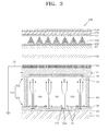
- FIG. 3 is a schematic cross-sectional view of an electron emission type backlight unit 100 according to another embodiment of the present invention.
- the backlight unit 100 includes an electron emission device 101 and a front panel 102 that form a light emitting space 103 therebetween, and spacers 160 disposed to maintain a distance between the electron emission device 101 and the front panel 102.
- the electron emission device 101 includes a first substrate 110, a plurality of first electrodes 120, an insulating layer 130, a plurality of second electrodes 140, and a plurality of electron emission sources 150.
- the front panel 102 includes a second substrate 171, a phosphor layer 175, a third electrode 173, and a wire grid polarizer 180.
- a diffusion sheet 190 is disposed on the backlight unit 100 and an LCD panel 200 is disposed on the diffusion sheet 190.
- the current embodiment differs from the previous embodiment in that one side of the wire grid polarizer 180 is grounded.
- a voltage is applied to a surface of the third electrode 173 which is an anode, and thus, static electricity may be generated on an external surface of the second substrate 171.
- Static electricity is one of a number of factors that cause a device to unstably operate, and may cause unnecessary particles, such as dust, to stick to an external surface of the backlight unit 100.
- one side of the wire grid polarizer 180 of the backlight unit 100 according to the current embodiment is grounded (see reference numeral G1 of FIG. 3 ). That is, the wire grid polarizer 180 includes a conductor, and thus, one side of the wire grid polarizer 180 is grounded, thereby reducing occurence of static electricity.
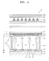
- FIG. 4 is a schematic cross-sectional view of an electron emission type backlight unit 100 according to another embodiment of the present invention.
- the backlight unit 100 includes an electron emission device 101 and a front panel 102 that form a light emitting space 103 therebetween, and spacers 160 disposed to maintain a distance between the electron emission device 101 and the front panel 102.
- the electron emission device 101 includes a first substrate 110, a plurality of first electrodes 120, an insulating layer 130, a plurality of second electrodes 140, and a plurality of electron emission sources 150.
- the front panel 102 includes a second substrate 371, a third electrode 373, a phosphor layer 375, and a wire grid polarizer 380.
- a diffusion sheet 190 is disposed on the backlight unit 100 and an LCD panel 200 is disposed on the diffusion sheet 190.
- the current embodiment differs from the previous embodiments in that the wire grid polarizer 380 is disposed on the second substrate 371 facing the first substrate 110. More specifically, the wire grid polarizer 380, the phosphor layer 375, and the third electrode 373 are sequentially formed on the second substrate 371 facing the first substrate 110, and the wire grid polarizer 380 and the phosphor layer 375 are directly adjacent and closely adhered to each other. In the current embodiment, since the second substrate 371 is not disposed between a rear surface of the wire grid polarizer 380 and the third electrode 373, an optical loss due to reflected light passing through the second substrate 371 may be reduced.
- the phosphor layer 375 is surrounded by the third electrode 373 and the wire grid polarizer 380 which may both include conductive materials. Thus, electrons colliding against the phosphor layer 375 are not discharged to the outside, preventing a voltage drop.
- one side of each of the wire grid polarizer 380 and the third electrode 373 may be connected to the same potential (see reference numeral G2 of FIG. 4 ). That is, the wire grid polarizer 380 and the third electrode 373 include conductive materials, and thus, one side of each of the wire grid polarizer 380 and the third electrode 373 is connected to apply an appropriate voltage thereto, thereby reducing occurrence of static electricity.
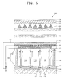
- FIG. 5 is a schematic cross-sectional view of an electron emission type backlight unit 100 according to another embodiment of the present invention.
- the backlight unit 100 includes an electron emission device 101 and a front panel 102 that form a light emitting space 103, and spacers 160 disposed to maintain a predetermined space between the electron emission device 101 and the front panel 102.
- the electron emission device 101 includes a first substrate 110, a plurality of first electrodes 120, an insulating layer 130, a plurality of second electrodes 140, and a plurality of electron emission sources 150.
- the front panel 102 includes a second substrate 471, a third electrode 473, a phosphor layer 375, and a wire grid polarizer 480.
- a diffusion sheet 190 is disposed on the backlight unit 100 and an LCD panel 200 is disposed on the diffusion sheet 190.
- the current embodiment differs from the embodiment of FIG. 4 in that a static electricity prevention layer 485 is further disposed on the second substrate 471.
- the static electricity prevention layer 485 may be further formed on the second substrate 471 facing the diffusion sheet 190 and the LCD panel 200, and one side of the static electricity prevention layer 485 may further be grounded (see reference numeral G3 of FIG. 5 ).
- the above exemplary embodiments of a backlight unit according to the present invention provide improved luminous efficiency.
Landscapes
- Physics & Mathematics (AREA)
- Nonlinear Science (AREA)
- Mathematical Physics (AREA)
- Chemical & Material Sciences (AREA)
- Crystallography & Structural Chemistry (AREA)
- General Physics & Mathematics (AREA)
- Optics & Photonics (AREA)
- Liquid Crystal (AREA)
- Planar Illumination Modules (AREA)
- Optical Elements Other Than Lenses (AREA)
- Polarising Elements (AREA)
- Discharge Lamps And Accessories Thereof (AREA)
Applications Claiming Priority (1)
| Application Number | Priority Date | Filing Date | Title |
|---|---|---|---|
| KR1020080111873A KR100975876B1 (ko) | 2008-11-11 | 2008-11-11 | 백라이트 유닛 |
Publications (1)
| Publication Number | Publication Date |
|---|---|
| EP2184635A1 true EP2184635A1 (de) | 2010-05-12 |
Family
ID=41395522
Family Applications (1)
| Application Number | Title | Priority Date | Filing Date |
|---|---|---|---|
| EP09175695A Withdrawn EP2184635A1 (de) | 2008-11-11 | 2009-11-11 | Rückbeleuchtungseinheit mit fest eingebautem Drahtgitter-Polarisator |
Country Status (5)
| Country | Link |
|---|---|
| US (1) | US20100118222A1 (de) |
| EP (1) | EP2184635A1 (de) |
| JP (1) | JP2010118342A (de) |
| KR (1) | KR100975876B1 (de) |
| CN (1) | CN101742750A (de) |
Families Citing this family (11)
| Publication number | Priority date | Publication date | Assignee | Title |
|---|---|---|---|---|
| TWI437612B (zh) * | 2010-12-16 | 2014-05-11 | Tatung Co | 場發射光源裝置 |
| TWI450391B (zh) * | 2010-12-23 | 2014-08-21 | Advanced Optoelectronic Tech | 發光二極體立體顯示器 |
| JP2012238632A (ja) * | 2011-05-10 | 2012-12-06 | Sony Corp | 固体撮像装置、固体撮像装置の製造方法、及び、電子機器 |
| CN105137649B (zh) * | 2015-10-23 | 2018-01-12 | 深圳市华星光电技术有限公司 | 一种液晶显示面板 |
| CN105700212A (zh) * | 2016-04-11 | 2016-06-22 | 京东方科技集团股份有限公司 | 一种显示装置 |
| CN105929593A (zh) * | 2016-07-11 | 2016-09-07 | 京东方科技集团股份有限公司 | 阵列基板、透明显示基板和透明显示装置 |
| KR102581143B1 (ko) * | 2016-08-18 | 2023-09-21 | 삼성디스플레이 주식회사 | 표시 장치 |
| TWI631392B (zh) * | 2017-05-23 | 2018-08-01 | 明基材料股份有限公司 | 背光模組 |
| CN107193158B (zh) | 2017-06-15 | 2020-04-17 | 京东方科技集团股份有限公司 | 一种背光模组、显示装置及背光模组的制备方法 |
| JP6609351B1 (ja) * | 2018-06-18 | 2019-11-20 | デクセリアルズ株式会社 | 偏光板およびその製造方法 |
| CN109375419B (zh) * | 2018-10-29 | 2021-11-05 | 京东方科技集团股份有限公司 | 背光模组和显示装置 |
Citations (11)
| Publication number | Priority date | Publication date | Assignee | Title |
|---|---|---|---|---|
| US5760858A (en) * | 1995-04-21 | 1998-06-02 | Texas Instruments Incorporated | Field emission device panel backlight for liquid crystal displays |
| KR20040000769A (ko) * | 2002-06-25 | 2004-01-07 | 엘지.필립스 엘시디 주식회사 | 액정표시장치 모듈 |
| US20040080926A1 (en) | 2002-10-23 | 2004-04-29 | Hannstar Display Corp. | Polarized light source device and back light module for liquid crystal display |
| US20070024545A1 (en) | 2005-07-27 | 2007-02-01 | Young-Suk Cho | Electron emission type backlight unit and flat panel display device having the same |
| US20070047214A1 (en) | 2005-08-30 | 2007-03-01 | Samsung Electronics Co., Ltd. | Backlight unit using wire-grid polarizer and liquid crystal display apparatus employing the backlight unit |
| JP2007219340A (ja) * | 2006-02-20 | 2007-08-30 | Epson Toyocom Corp | 複合ワイヤーグリッド偏光子、複合光学素子及び偏光光源 |
| US20070247566A1 (en) | 2006-04-19 | 2007-10-25 | Dae Ho Choo | Liquid crystal display module |
| EP1855144A1 (de) * | 2005-07-15 | 2007-11-14 | Sanyo Electric Co., Ltd. | Beleuchtungsvorrichtung und projektorähnliches Videoanzeigegerät |
| JP2008145649A (ja) * | 2006-12-08 | 2008-06-26 | Sony Corp | 液晶表示装置および投射型表示装置 |
| US20080259242A1 (en) | 2007-01-23 | 2008-10-23 | Pentax Corporation | Polarized light emitting device |
| WO2009105450A1 (en) * | 2008-02-22 | 2009-08-27 | 3M Innovative Properties Company | Backlights having selected output light flux distributions and display systems using same |
Family Cites Families (9)
| Publication number | Priority date | Publication date | Assignee | Title |
|---|---|---|---|---|
| JPH08248418A (ja) * | 1995-03-08 | 1996-09-27 | Toshiba Lighting & Technol Corp | バックライト,液晶表示装置および表示装置 |
| JP2002090735A (ja) * | 2000-09-13 | 2002-03-27 | Canon Inc | 電子機器 |
| US6846089B2 (en) * | 2003-05-16 | 2005-01-25 | 3M Innovative Properties Company | Method for stacking surface structured optical films |
| JP3735361B2 (ja) * | 2003-08-07 | 2006-01-18 | 日東電工株式会社 | 光学フィルムの製造方法、それにより得られた光学フィルム、液晶パネルおよび液晶表示装置 |
| US7466484B2 (en) * | 2004-09-23 | 2008-12-16 | Rohm And Haas Denmark Finance A/S | Wire grid polarizers and optical elements containing them |
| JP4683998B2 (ja) * | 2005-05-09 | 2011-05-18 | 富士フイルム株式会社 | 紫外線照射装置、光学補償シート、ならびにそれを用いた偏光板及び液晶表示装置 |
| JP4889239B2 (ja) * | 2005-05-18 | 2012-03-07 | チェイル インダストリーズ インコーポレイテッド | バックライトユニットおよび液晶表示装置 |
| JP4725456B2 (ja) * | 2006-08-09 | 2011-07-13 | セイコーエプソン株式会社 | 固体光源およびプロジェクタ |
| KR101350873B1 (ko) * | 2007-03-08 | 2014-01-13 | 삼성디스플레이 주식회사 | 액정 표시 장치 |
-
2008
- 2008-11-11 KR KR1020080111873A patent/KR100975876B1/ko not_active Expired - Fee Related
-
2009
- 2009-11-06 US US12/614,277 patent/US20100118222A1/en not_active Abandoned
- 2009-11-09 JP JP2009255951A patent/JP2010118342A/ja active Pending
- 2009-11-11 CN CN200910221279A patent/CN101742750A/zh active Pending
- 2009-11-11 EP EP09175695A patent/EP2184635A1/de not_active Withdrawn
Patent Citations (11)
| Publication number | Priority date | Publication date | Assignee | Title |
|---|---|---|---|---|
| US5760858A (en) * | 1995-04-21 | 1998-06-02 | Texas Instruments Incorporated | Field emission device panel backlight for liquid crystal displays |
| KR20040000769A (ko) * | 2002-06-25 | 2004-01-07 | 엘지.필립스 엘시디 주식회사 | 액정표시장치 모듈 |
| US20040080926A1 (en) | 2002-10-23 | 2004-04-29 | Hannstar Display Corp. | Polarized light source device and back light module for liquid crystal display |
| EP1855144A1 (de) * | 2005-07-15 | 2007-11-14 | Sanyo Electric Co., Ltd. | Beleuchtungsvorrichtung und projektorähnliches Videoanzeigegerät |
| US20070024545A1 (en) | 2005-07-27 | 2007-02-01 | Young-Suk Cho | Electron emission type backlight unit and flat panel display device having the same |
| US20070047214A1 (en) | 2005-08-30 | 2007-03-01 | Samsung Electronics Co., Ltd. | Backlight unit using wire-grid polarizer and liquid crystal display apparatus employing the backlight unit |
| JP2007219340A (ja) * | 2006-02-20 | 2007-08-30 | Epson Toyocom Corp | 複合ワイヤーグリッド偏光子、複合光学素子及び偏光光源 |
| US20070247566A1 (en) | 2006-04-19 | 2007-10-25 | Dae Ho Choo | Liquid crystal display module |
| JP2008145649A (ja) * | 2006-12-08 | 2008-06-26 | Sony Corp | 液晶表示装置および投射型表示装置 |
| US20080259242A1 (en) | 2007-01-23 | 2008-10-23 | Pentax Corporation | Polarized light emitting device |
| WO2009105450A1 (en) * | 2008-02-22 | 2009-08-27 | 3M Innovative Properties Company | Backlights having selected output light flux distributions and display systems using same |
Also Published As
| Publication number | Publication date |
|---|---|
| CN101742750A (zh) | 2010-06-16 |
| KR20100052958A (ko) | 2010-05-20 |
| US20100118222A1 (en) | 2010-05-13 |
| JP2010118342A (ja) | 2010-05-27 |
| KR100975876B1 (ko) | 2010-08-13 |
Similar Documents
| Publication | Publication Date | Title |
|---|---|---|
| US20100118222A1 (en) | Backlight unit | |
| EP1746634B1 (de) | Elektronenemissionsvorrichtung, Elektronenemissionsrückbeleuchtungseinheit und Flachbildschirmgerät mit derselben | |
| KR20050072945A (ko) | 전계방출형 백라이트 유니트 및 그 구동 방법과 하부패널의 제조 방법 | |
| JP2005243632A (ja) | 弾道電子の表面放出装置エミッタ、それを採用した電界放出表示装置及び電界放出型バックライト素子 | |
| KR20050086238A (ko) | 전계 방출 표시장치 | |
| US7525244B2 (en) | Field emission type backlight device | |
| EP1746628B1 (de) | Elektronenemissionsvorrichtung, Elektronenemissionsrückbeleuchtungseinheit und Flachbildschirmgerät mit derselben | |
| EP1814141B1 (de) | Elektronenemissionsvorrichtung, Hintergrundbeleuchtungseinheit (BLU) mit Elektronenemissionsvorrichtung, Flachbildschirm mit BLU und Ansteuerungsverfahren für die Elektronenemissionsvorrichtung | |
| US7960906B2 (en) | Electron emission device, light emission apparatus including the same, and method of manufacturing the electron emission device | |
| EP1746620B1 (de) | Hintergrundbeleuchtungseinheit mit Elektronen-Emissionseinrichtung, sowie Flachbildschirm mit dieser Einheit | |
| US20080278062A1 (en) | Method of fabricating electron emission source, electron emission device, and electron emission display device including the electron emission device | |
| JP2006332044A (ja) | 熱電子放出バックライト装置 | |
| JP2007294406A (ja) | 電子放出表示素子 | |
| US20090310333A1 (en) | Electron emission device, electron emission type backlight unit including the same, and method of manufacturing the electron emission device | |
| JP2007035633A (ja) | 電子放出型バックライトユニット及びそれを備えた平板ディスプレイ装置 | |
| JPH08293272A (ja) | 画像表示装置 | |
| US7994696B2 (en) | Electron emission device, electron emission type backlight unit including the electron emission device, and method of manufacturing the electron emission device | |
| KR20060113192A (ko) | 전자 방출 소자 및 그 제조 방법 | |
| KR101000662B1 (ko) | 전계 방출 소자 | |
| KR20050077962A (ko) | 전계 방출 표시장치 | |
| KR20070103909A (ko) | 전자 방출 표시 디바이스 | |
| KR20070010806A (ko) | 전자 방출 소자, 이를 구비한 평판 디스플레이 장치 및 그제조 방법 | |
| KR20070014495A (ko) | 전자방출표시장치의 잔사 제거방법 | |
| KR20070046630A (ko) | 전자 방출 표시소자 | |
| KR20070024955A (ko) | 전자 방출 소자 및 이를 구비한 평판 디스플레이 장치 |
Legal Events
| Date | Code | Title | Description |
|---|---|---|---|
| PUAI | Public reference made under article 153(3) epc to a published international application that has entered the european phase |
Free format text: ORIGINAL CODE: 0009012 |
|
| 17P | Request for examination filed |
Effective date: 20091111 |
|
| AK | Designated contracting states |
Kind code of ref document: A1 Designated state(s): AT BE BG CH CY CZ DE DK EE ES FI FR GB GR HR HU IE IS IT LI LT LU LV MC MK MT NL NO PL PT RO SE SI SK SM TR |
|
| AX | Request for extension of the european patent |
Extension state: AL BA RS |
|
| 17Q | First examination report despatched |
Effective date: 20101115 |
|
| GRAP | Despatch of communication of intention to grant a patent |
Free format text: ORIGINAL CODE: EPIDOSNIGR1 |
|
| RIC1 | Information provided on ipc code assigned before grant |
Ipc: H01J 63/06 20060101ALI20110505BHEP Ipc: G02F 1/13357 20060101AFI20110505BHEP |
|
| RIN1 | Information on inventor provided before grant (corrected) |
Inventor name: LEE, BYONG-GON |
|
| STAA | Information on the status of an ep patent application or granted ep patent |
Free format text: STATUS: THE APPLICATION IS DEEMED TO BE WITHDRAWN |
|
| 18D | Application deemed to be withdrawn |
Effective date: 20111012 |