EP2182565A1 - Light emitting display and method of manufacturing the same - Google Patents
Light emitting display and method of manufacturing the same Download PDFInfo
- Publication number
- EP2182565A1 EP2182565A1 EP09252487A EP09252487A EP2182565A1 EP 2182565 A1 EP2182565 A1 EP 2182565A1 EP 09252487 A EP09252487 A EP 09252487A EP 09252487 A EP09252487 A EP 09252487A EP 2182565 A1 EP2182565 A1 EP 2182565A1
- Authority
- EP
- European Patent Office
- Prior art keywords
- substrate
- light emitting
- dam member
- emitting display
- sealing material
- Prior art date
- Legal status (The legal status is an assumption and is not a legal conclusion. Google has not performed a legal analysis and makes no representation as to the accuracy of the status listed.)
- Granted
Links
Images



Classifications
-
- H—ELECTRICITY
- H10—SEMICONDUCTOR DEVICES; ELECTRIC SOLID-STATE DEVICES NOT OTHERWISE PROVIDED FOR
- H10K—ORGANIC ELECTRIC SOLID-STATE DEVICES
- H10K59/00—Integrated devices, or assemblies of multiple devices, comprising at least one organic light-emitting element covered by group H10K50/00
- H10K59/80—Constructional details
- H10K59/87—Passivation; Containers; Encapsulations
- H10K59/871—Self-supporting sealing arrangements
- H10K59/8722—Peripheral sealing arrangements, e.g. adhesives, sealants
-
- H—ELECTRICITY
- H10—SEMICONDUCTOR DEVICES; ELECTRIC SOLID-STATE DEVICES NOT OTHERWISE PROVIDED FOR
- H10K—ORGANIC ELECTRIC SOLID-STATE DEVICES
- H10K59/00—Integrated devices, or assemblies of multiple devices, comprising at least one organic light-emitting element covered by group H10K50/00
- H10K59/80—Constructional details
- H10K59/87—Passivation; Containers; Encapsulations
- H10K59/871—Self-supporting sealing arrangements
- H10K59/872—Containers
-
- H—ELECTRICITY
- H10—SEMICONDUCTOR DEVICES; ELECTRIC SOLID-STATE DEVICES NOT OTHERWISE PROVIDED FOR
- H10K—ORGANIC ELECTRIC SOLID-STATE DEVICES
- H10K71/00—Manufacture or treatment specially adapted for the organic devices covered by this subclass
Definitions
- the present invention relates to a light emitting display and a method of manufacturing the same, and more particularly to, a light emitting display having an inert liquid filling material between a substrate on which a light emitting device is formed and a sealing substrate, and a method of manufacturing the same.
- a light emitting device such as an organic light emitting diode (OLED) includes organic materials vulnerable to moisture or oxygen, it is desirable to protect the OLED against moisture and/or oxygen using a sealing member.
- OLED organic light emitting diode
- a light emitting display using an OLED typically has a wide viewing angle, high contrast and response speed, and low power consumption, in spite of its vulnerability to moisture or oxygen, light emitting displays are widely used in personal portable apparatuses, such as MP3 players, mobile telephones, and televisions (TV). The thicknesses of light emitting displays have been gradually reduced in accordance with the requests of users.
- a light emitting display including: a first substrate on which a plurality of light emitting devices are formed; a second substrate disposed to face the first substrate; a dam member disposed between the first substrate and the second substrate to surround the plurality of light emitting devices; an inorganic sealing material disposed between the first substrate and the second substrate on an outward side of the dam member and attaching the first substrate and the second substrate; and a filling material provided between the first substrate and the second substrate on an inward side of the dam member and formed of at least one inert liquid selected from the group consisting of perfluorocarbon and fluorinert.
- the light emitting devices may comprise first electrodes, organic light emitting layers and second electrodes.
- the filling material may be provided between the first substrate and the second substrate to be in contact with the second electrodes.
- the dam member may comprise an inorganic material.
- the inorganic material may comprise frit.
- a reflecting layer that reflects a laser or infrared rays may be formed on a surface of the dam member.
- the reflecting layer may comprise at least one selected from the group consisting of Au, Ag, Pt, and Al.
- the dam member may be disposed to be in contact with the inorganic sealing material.
- the dam member may comprise an organic material.
- the organic material may comprise at least one selected from the group consisting of epoxy, epoxy acrylate, bisphenol A type epoxy, cycloaliphatic epoxy resin, phenyl silicone resin or rubber, and acrylic epoxy resin.
- the dam member may be disposed to be separated from the inorganic sealing material.
- the dam member and the inorganic sealing material may be separated from each other by at least about 50 ⁇ m.
- the inorganic sealing material may comprise frit.
- the frit may be melted by a laser or infrared rays.
- the frit may comprise a transition metal compound.
- a method of manufacturing a light emitting display including: providing a first substrate on which a plurality of light emitting devices are formed; providing a second substrate; forming an inorganic sealing material along an edge of the second substrate; forming a dam member on the second substrate on an inward side of the inorganic sealing material to surround the plurality of light emitting devices; dropping a filling material to an inward side of the dam member, the filling material being formed of at least one inert liquid selected from the group consisting of perfluorocarbon and fluorinert; disposing the first substrate and the second substrate to face each other; and attaching the inorganic sealing material to the first substrate and the second substrate to seal the plurality of light emitting devices.
- the forming the inorganic sealing material may comprise applying frit paste; and drying or annealing the applied frit paste.
- the forming the dam member may comprise: applying frit paste; and drying or annealing the applied frit paste and hardening the frit paste.
- the dam member may be formed to be in contact with the inorganic sealing material.
- the forming the dam member may comprise: applying a liquid organic material to be separated from the inorganic sealing material; and pre-hardening the applied liquid organic material.
- the disposing the first substrate and the second substrate to face each other may be performed at a pressure lower than atmospheric pressure.
- the method may further comprise compressing the first substrate and the second substrate so that the filling material fills a space between the first substrate and the second substrate on the inward side of the dam member.
- the sealing the light emitting devices may further comprise attaching the first substrate to the second substrate by melting the inorganic sealing material.
- the inorganic sealing material may be melted by a laser or infrared rays.
- the present invention as described above seals an light emitting device using an inorganic sealing material which effectively blocks hydrogen or oxygen and fills a space between substrates with an inert liquid filling material to improve pressure resistance.
- the inert liquid filling material such as a perfluorocarbon or fluorinert, is a colorless, odorless, nontoxic and inert material, has a high stability not to react to the material of the light emitting device, and maintains pressure resistance between the substrates to allow a sealed state not to be easily broken by means of impact or the like. Therefore, mechanical reliability is improved so that the life of a light emitting display can be increased, and a passivation film for protecting a cathode electrode is omitted to simplify the manufacturing process.
- the substrate may droop to generate Newton's ring or the display is vulnerable to impact.
- the space between the substrate and the sealing substrate is filled with a liquid filling material with a refractivity similar to the refractivity of a glass substrate, so that Newton's ring does not occur and visibility is high.
- a light emitting display as set out in Claim 1. Preferred features of this aspect are set out in Claims 2 to 13.
- FIG. 1 is a perspective view illustrating a light emitting display according to an embodiment of the present invention
- FIG. 2 is a cross-sectional view taken along section line I1-I2 of FIG. 1 ;
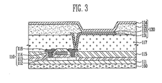
- FIG. 3 is a cross-sectional view illustrating the light emitting device of FIG. 1 ;
- FIGS. 4A and 4B are plan views illustrating an embodiment of a method of manufacturing the light emitting display according to the present invention.
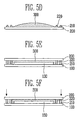
- FIGS. 5A to 5F are cross-sectional views illustrating the embodiment of the method of manufacturing the light emitting display according to the present invention.
- first element when a first element is described as being coupled to a second element, the first element may be not only directly coupled to the second element but may also be indirectly coupled to the second element via one or more third elements. Further, elements that are not essential to a complete understanding are omitted for clarity. Also, like reference numerals refer to like elements throughout.
- an inorganic sealing material that effectively prevents moisture or oxygen from penetrating.
- the inorganic sealing material easily falls off by means of impact or twisting to deteriorate mechanical reliability.
- embodiments of the present invention provide a light emitting display capable of increasing a life and of improving mechanical reliability using an inorganic sealing material that effectively prevents moisture or oxygen from penetrating and a method of manufacturing the same.
- FIG. 1 is a perspective view illustrating a light emitting display according to an embodiment of the present invention
- FIG. 2 is a cross-sectional view taken along section line I1-I2 of FIG. 1 .
- the light emitting display of this embodiment the present invention includes a substrate 100 on which a plurality of light emitting devices 130 are formed, a sealing substrate 200 disposed to face the substrate 100, a dam member 220 provided between the substrate 100 and the sealing substrate 200 to surrounds the plurality of light emitting devices 130, an inorganic sealing material 210 provided between the substrate 100 and the sealing substrate 200 outside the dam member 220 to attach the substrate 100 to the sealing substrate 200, and an inert liquid filling material 300 provided between the substrate 100 and the sealing substrate 200 inside the dam member 220.
- the substrate 100 is defined as a pixel region 120 and a non-pixel region 140 around the pixel region 120.
- the plurality of light emitting devices 130 are formed in the pixel region 120, and a driving circuit 160 for driving the plurality of light emitting devices 130 is formed in the non-pixel region 140.
- the light emitting devices 130 may be organic light emitting diodes (OLEDs) that include anode electrodes 131, cathode electrodes 134 and organic light emitting layers 133 formed between the anode electrodes 131 and the cathode electrodes 134.
- OLEDs organic light emitting diodes
- the organic light emitting layers 133 are formed in a light emitting region (a region where the anode electrode 131 is exposed) defined by a pixel definition layer 132 and may include a hole injection layer, a hole transport layer, an electron transport layer and an electron injection layer.
- the light emitting device 130 may be coupled to a thin film transistor for controlling the operation and a capacitor for maintaining a signal.
- the thin film transistor 110 includes a semiconductor layer 112 providing a source and drain region and a channel region, a gate electrode 114 insulated from the semiconductor layer 112 by a gate insulating layer 113, and a source and drain electrode 116 coupled to the semiconductor layer 112 in the source and drain region through a contact hole formed in the insulating layer 115 and the gate insulating layer 113.
- Reference numerals 111 and 117 are a buffer layer and a planarization layer, respectively.
- the sealing substrate 200 is provided to overlap with the pixel region 120 and a part of the non-pixel region 140.
- the sealing substrate 200 can be formed of a transparent material such as glass.
- the sealing substrate 200 can be formed of an opaque material.
- the inorganic sealing material 210 includes frit, which is melted by a laser or infrared rays to be attached to the substrate 100 and the sealing substrate 200.
- the inorganic sealing material 210 is provided between the substrate 100 and the sealing substrate 200 to surround the light emitting devices 130 so that the infiltration of moisture or oxygen from the outside is prevented.
- the dam member 220 prevents the filling material 300 from flowing to keep the filling material 300 in shape.
- the dam member 220 is provided to prevent heat from being transmitted to the light emitting devices 130 while the inorganic sealing material 210 is attached to the substrate 100 and the sealing substrate 200.
- the dam member 220 is formed of an inorganic material or an organic material.
- the inorganic material may employ frit.
- frit that transmits or reflects a laser or infrared rays is used or a reflecting layer is formed on the surface of the dam member 220 using metal having a high reflectance in an infrared region such as Au, Ag, Pt, Al, or the like so that a laser or infrared rays are reflected.
- the organic material may use at least one material selected from the group consisting of epoxy, epoxy acrylate, and silicones (such as bisphenol A type epoxy, cycloaliphatic epoxy resin, phenyl silicone resin or rubber, acrylic epoxy resin, and the like).
- the dam member 220 may be formed to be in contact with the inorganic sealing material 210 or to be parallel separated from the inorganic sealing material 210 by a predetermined distance.
- the dam member 220 may be in contact with the inorganic sealing material 210 when the dam member 220 includes an inorganic material, and may be separated from the inorganic sealing material 210 by 50 ⁇ m or more when the dam member 220 includes an organic material.
- the dam member 220 of an organic material is formed to be in contact with the inorganic sealing material 210, the dam member 220 is thermally decomposed while the inorganic sealing material 210 is attached to the substrate 100 and the sealing substrate 200, thereby generating out gas.
- the inert filling material 300 is provided to fill an inner space defined by the dam member 220, and thus it preferably employs a colorless material having a transmittance of not less than 90% in a visible region such as a glass substrate. Also, the inert filing material 300 preferably has a high stability not reacting to the material of the light emitting device 130.
- An inert liquid used as the filling material 300 may be an inert fluorocarbon based liquid.
- the inert liquid may be a perfluorocarbon based liquid, for example a perfluorocarbon or a mixture of perfluorocarbons.
- the inert liquid may be selected from the group consisting of one or more perfluorocarbons and fluorinert.
- the inert liquid can therefore be a colorless, odorless, nontoxic and inert material that has a high stability so that it does not react to an electrode formed of a metal material, in particular, the cathode electrode 134.
- an organic or inorganic passivation film (not shown) is required to be formed on the cathode electrode 134. In this case, however, a more process is involved and the thickness of the display becomes thicker.
- embodiments of the present invention uses the filling material 300 formed of an inert liquid not reacting to a metal material, it can be implemented to have a structure where the cathode electrode 134 is exposed, making it possible to simplify the process and structure thereof.
- FIGS. 4A and 4B are plan views illustrating a method of manufacturing the light emitting display according to the present invention.
- FIGS. 5A to 5F are cross-sectional views illustrating the method of manufacturing the light emitting display according to the present invention, taken along section line I11-I12 of FIG. 4B .
- the substrate 100 on which the plurality of light emitting devices 130 are formed is provided.
- the substrate 100 is divided into the pixel region 120 and the non-pixel region 140 around the pixel region 120.
- the plurality of light emitting devices 130 can be formed in the pixel region 120 of the substrate 100, and the driving circuit 160 for driving the light emitting devices 130 can be formed in the non-pixel region 140.
- the light emitting devices 130 include the OLEDs having the anode electrodes, the organic light emitting layers, and the cathode electrodes. Also, it may further include thin film transistors (TFTs) for controlling the operation of the OLEDs and capacitors for maintaining signals.
- TFTs thin film transistors
- a process of manufacturing an OLED is illustrated in the Korean Patent Publications No. 2002-0047889 (published on June 22, 2002 ) and No. 2003-0092873 (published on December 6, 2003 ), the entire disclosures of which are incorporated by reference.
- the sealing substrate 200 for sealing the light emitting devices 130 of the pixel region 120 is provided.
- the sealing substrate 200 may overlap with the pixel region 120 and a part of the non-pixel region 140.
- the sealing substrate 200 employs a transparent substrate such as glass in case of a front emission structure or an opaque substrate in case of a rear emission type.
- An inorganic sealing material 210 is formed along the edge of the sealing substrate 200.
- the inorganic sealing material 210 may employ frit and be formed by applying using dispensers or a screen printing method. Frit commonly means a powdery glass material. However, in the present embodiment of the invention, frit refers to paste including a main material such as SiO2 mixed with a laser or infrared ray absorbing material, an organic binder, and a filler for reducing a thermal expansion coefficient. The frit in paste is hardened, as the organic binder and moisture are removed from the frit via a drying or annealing process.
- the laser or infrared ray absorbing material may include a transition metal compound, for example, a vanadium compound.
- the dam member 220 is formed on the sealing substrate 200 on the inward side of the inorganic sealing material 210 to surround the pixel region 120.
- the dam member 220 may use an inorganic material or an organic material, and be applied by dispensers or screen printing. At this time, the amount of the inorganic material or organic material is determined in consideration of the distance from an outmost light emitting device 130 in the pixel region 120 to the inorganic sealing material 210 and the height of the dam member 220.
- the height of the dam member 220 is determined by the height of the inorganic sealing material 210 and is preferably adjusted to be equal to or lower than the height of the inorganic sealing material 210.
- the inorganic material may employ frit.
- the dam member 220 can be formed in a process of forming the inorganic sealing material 210.
- frit that transmits or reflects a laser or infrared rays is used or a reflecting layer 222 is formed on the surface of the dam member 220 in order to reflect a laser or infrared rays, as illustrated in FIG. 5B .
- the frit is hardened to form the dam member 220.
- metal such as Au, Ag, Pt, or Al having a high reflectance in the infrared region is applied to the surface of the dam member 220 to form the reflecting layer 222.
- the organic material may employ a material selected from the group consisting of epoxy, epoxy acrylate, and silicones (such as bisphenol A type epoxy, cycloaliphatic epoxy resin, phenyl silicone resin or rubber, acrylic epoxy resin, etc.).
- the dam member 220 is formed to be in contact with the inorganic sealing material 210, as illustrated in FIG. 5B , or to be separated from the inorganic sealing material 210 by a predetermined distance, as illustrated in FIG. 5C .
- the dam member 220 is formed of an inorganic material, it is in contact with the inorganic sealing material 210. In this case, the area of the non-pixel region, i.e., a dead space, may be reduced.
- the dam member 220 is preferably separated from the inorganic sealing material 210 by no less than about 50 ⁇ m.
- the dam member 220 may be easily collapsed by stress such as a pressure difference. Therefore, the dam member 220 is formed and then pre-hardened so that it becomes solid in structure to enhance its function.
- the dam member 220 is pre-hardened by heat, an electron beam, or an ultraviolet ray in accordance with the kind of the organic material and so as not to be damaged by stress in a process of attaching the substrate 100 to the sealing substrate 200.
- a dummy sealing material (not shown) may be formed of epoxy, frit, etc. along the outermost edge of the sealing substrate 200.
- the dummy sealing material is formed outside the inorganic sealing material 210 to collectively seal up the space between the substrate 100 and the sealing substrate 200. In the case of a mother substrate, the dummy sealing material is disposed on the outermost edge thereof.
- the inert liquid filling material 300 is provided on the sealing substrate 200 on the inward side of the region defined by the dam member 220.
- the filling material 300 is preferably a colorless material having a transmittance of not less than about 90% in a visible ray region and has stability not reacting to the material of the light emitting devices 130.
- An inert liquid used as the filling material 300 may be an inert fluorocarbon based liquid.
- the inert liquid may be a perfluorocarbon based liquid, for example a perfluorocarbon or a mixture of perfluorocarbons.
- the inert liquid may be selected from the group consisting of perfluorocarbon and fluorinert.
- the filling material 300 may be provided using ink jetting, dispensers, screen printing, one drop filling (ODF) or the like.
- ODF one drop filling
- the proper amount of the filling material 300 can be dropped to the sealing substrate 200 on the inward side of the dam member 220 using a one drop filling (ODF) device.
- ODF one drop filling
- the substrate 100 is disposed to face the sealing substrate 200.
- the substrate 100 is mounted on an upper chuck of an attaching device and the sealing substrate 200 is mounted on a lower chuck of the attaching device, and then the substrate 100 and the sealing substrate 200 are attached to each other.
- the light emitting devices 130 are covered with the filling material 300, and the flow of the filling material 300 is prevented by the dam member 220 so that the filling material is kept in shape.
- the substrate 100 and the sealing substrate 200 are attached to each other under a pressure lower than atmospheric pressure so as not to form bubbles or voids between the substrate 100 and the sealing substrate 200.
- the substrate 100 and the sealing substrate 200 are pressed together so that the space between the light emitting devices 130 and the sealing substrate 200 is completely filled with the filling material 300.
- a laser or infrared rays are irradiated along the inorganic sealing material 210 while the substrate 100 and the sealing substrate 200 are attached to each other.
- the inorganic sealing material 210 is melted to be attached to the substrate 100 and the sealing substrate 200, and accordingly the light emitting devices 130 are sealed.
- Such a sealing process is performed preferably after the dummy sealing material is hardened so that the space between the substrate 100 and the sealing substrate 200 is kept a vacuum.
- a mask or a protecting film (not shown) is used to irradiate the laser and infrared rays only to a desired region.
- the dam member 220 includes an inorganic material that transmits or reflects a laser or infrared rays or when the reflecting layer 222 is disposed on the surface of the dam member 220, the mask or the protecting film is disposed only in the pixel region 120 so that the laser or infrared rays are not irradiated.
- the dam member 220 includes an organic material
- the mask or the protecting film is disposed in the pixel region 120 and the non-pixel region 140 where the dam member 220 is formed so that the laser or infrared rays do not irradiated.
- the inorganic sealing material 210 may further seal the driving circuit 160.
- the inorganic sealing material 210 and the dam member 220 are described as being integrated with each other on the sealing substrate 200, but may be integrated with each other on the substrate 100 and may have a double or multiple structure.
- the inorganic sealing material 210 may be formed in a double or multiple structure, or the dam member 220 may have a double or multiple structure in order to improve heat shielding effect.
- the filling material 300 is filled before attaching the substrate 100 and the sealing substrate 200 to each other.
- the filling material 300 may be filled after the substrate 100 and the sealing substrate 200 are attached to each other in accordance with the properties of material.
Landscapes
- Engineering & Computer Science (AREA)
- Manufacturing & Machinery (AREA)
- Electroluminescent Light Sources (AREA)
- Devices For Indicating Variable Information By Combining Individual Elements (AREA)
Abstract
Description
- The present invention relates to a light emitting display and a method of manufacturing the same, and more particularly to, a light emitting display having an inert liquid filling material between a substrate on which a light emitting device is formed and a sealing substrate, and a method of manufacturing the same.
- Since a light emitting device such as an organic light emitting diode (OLED) includes organic materials vulnerable to moisture or oxygen, it is desirable to protect the OLED against moisture and/or oxygen using a sealing member.
- Since a light emitting display using an OLED typically has a wide viewing angle, high contrast and response speed, and low power consumption, in spite of its vulnerability to moisture or oxygen, light emitting displays are widely used in personal portable apparatuses, such as MP3 players, mobile telephones, and televisions (TV). The thicknesses of light emitting displays have been gradually reduced in accordance with the requests of users.
- However, when the thickness of a substrate of a light emitting display is reduced to no more than about 0.3 mm in order to reduce the thickness thereof, it is difficult to maintain the mechanical integrity of the device under stresses such as falling and twisting. Loss of mechanical integrity can compromise the sealed state of the device, thereby reducing the life of the organic light emitting display.
- Accordingly, it is an object to provide a light emitting display capable of securing mechanical reliability and of increasing a life and a method of manufacturing the same.
- It is another object to provide a light emitting display capable of securing mechanical reliability while using an inorganic sealing material that effectively prevents moisture or oxygen from penetrating and a method of manufacturing the same.
- In order to achieve the foregoing and/or other objects, according to one aspect of the present invention, there is provided a light emitting display including: a first substrate on which a plurality of light emitting devices are formed; a second substrate disposed to face the first substrate; a dam member disposed between the first substrate and the second substrate to surround the plurality of light emitting devices; an inorganic sealing material disposed between the first substrate and the second substrate on an outward side of the dam member and attaching the first substrate and the second substrate; and a filling material provided between the first substrate and the second substrate on an inward side of the dam member and formed of at least one inert liquid selected from the group consisting of perfluorocarbon and fluorinert.
- The light emitting devices may comprise first electrodes, organic light emitting layers and second electrodes.
- The filling material may be provided between the first substrate and the second substrate to be in contact with the second electrodes.
- The dam member may comprise an inorganic material.
- The inorganic material may comprise frit.
- A reflecting layer that reflects a laser or infrared rays may be formed on a surface of the dam member. The reflecting layer may comprise at least one selected from the group consisting of Au, Ag, Pt, and Al.
- The dam member may be disposed to be in contact with the inorganic sealing material.
- The dam member may comprise an organic material. The organic material may comprise at least one selected from the group consisting of epoxy, epoxy acrylate, bisphenol A type epoxy, cycloaliphatic epoxy resin, phenyl silicone resin or rubber, and acrylic epoxy resin.
- The dam member may be disposed to be separated from the inorganic sealing material. The dam member and the inorganic sealing material may be separated from each other by at least about 50 µm.
- The inorganic sealing material may comprise frit. The frit may be melted by a laser or infrared rays.
- The frit may comprise a transition metal compound.
In order to achieve the foregoing and/or other objects, according to another aspect of the present invention, there is provided a method of manufacturing a light emitting display including: providing a first substrate on which a plurality of light emitting devices are formed; providing a second substrate; forming an inorganic sealing material along an edge of the second substrate; forming a dam member on the second substrate on an inward side of the inorganic sealing material to surround the plurality of light emitting devices; dropping a filling material to an inward side of the dam member, the filling material being formed of at least one inert liquid selected from the group consisting of perfluorocarbon and fluorinert; disposing the first substrate and the second substrate to face each other; and attaching the inorganic sealing material to the first substrate and the second substrate to seal the plurality of light emitting devices. - The forming the inorganic sealing material may comprise applying frit paste; and drying or annealing the applied frit paste.
- The forming the dam member may comprise: applying frit paste; and drying or annealing the applied frit paste and hardening the frit paste.
- The dam member may be formed to be in contact with the inorganic sealing material.
- The forming the dam member may comprise: applying a liquid organic material to be separated from the inorganic sealing material; and pre-hardening the applied liquid organic material.
- The disposing the first substrate and the second substrate to face each other may be performed at a pressure lower than atmospheric pressure.
- The method may further comprise compressing the first substrate and the second substrate so that the filling material fills a space between the first substrate and the second substrate on the inward side of the dam member.
- The sealing the light emitting devices may further comprise attaching the first substrate to the second substrate by melting the inorganic sealing material.
- The inorganic sealing material may be melted by a laser or infrared rays.
- The present invention as described above seals an light emitting device using an inorganic sealing material which effectively blocks hydrogen or oxygen and fills a space between substrates with an inert liquid filling material to improve pressure resistance. The inert liquid filling material, such as a perfluorocarbon or fluorinert, is a colorless, odorless, nontoxic and inert material, has a high stability not to react to the material of the light emitting device, and maintains pressure resistance between the substrates to allow a sealed state not to be easily broken by means of impact or the like. Therefore, mechanical reliability is improved so that the life of a light emitting display can be increased, and a passivation film for protecting a cathode electrode is omitted to simplify the manufacturing process.
- Also, in a conventional light emitting display, since a space between a substrate and a sealing substrate is empty, the substrate may droop to generate Newton's ring or the display is vulnerable to impact. In the light emitting display according to the present invention, however, the space between the substrate and the sealing substrate is filled with a liquid filling material with a refractivity similar to the refractivity of a glass substrate, so that Newton's ring does not occur and visibility is high.
- According to a first aspect of the invention, there is provided a light emitting display as set out in Claim 1. Preferred features of this aspect are set out in Claims 2 to 13.
- According to a second aspect of the invention, there is provided a method as set out in Claim 14. Preferred features of this aspect are set out in Claims 15 to 22.
- These and/or other aspects and advantages of the invention will become apparent and more readily appreciated from the following description of the preferred embodiments, taken in conjunction with the accompanying drawings of which:
-
FIG. 1 is a perspective view illustrating a light emitting display according to an embodiment of the present invention; -
FIG. 2 is a cross-sectional view taken along section line I1-I2 ofFIG. 1 ; -
FIG. 3 is a cross-sectional view illustrating the light emitting device ofFIG. 1 ; -
FIGS. 4A and 4B are plan views illustrating an embodiment of a method of manufacturing the light emitting display according to the present invention; and -
FIGS. 5A to 5F are cross-sectional views illustrating the embodiment of the method of manufacturing the light emitting display according to the present invention. - Hereinafter, embodiments of the present invention will be described in detail with reference to the accompanying drawings. However, the embodiments set forth herein are provided so that those skilled in the art can fully understand the present invention and thus, the present invention can be embodied in different forms and should not be construed as limited to the embodiments set forth herein. Here, when a first element is described as being coupled to a second element, the first element may be not only directly coupled to the second element but may also be indirectly coupled to the second element via one or more third elements. Further, elements that are not essential to a complete understanding are omitted for clarity. Also, like reference numerals refer to like elements throughout.
- In order to increase the life of an organic light emitting display, it is useful to employ an inorganic sealing material that effectively prevents moisture or oxygen from penetrating. However, the inorganic sealing material easily falls off by means of impact or twisting to deteriorate mechanical reliability.
- Therefore, embodiments of the present invention provide a light emitting display capable of increasing a life and of improving mechanical reliability using an inorganic sealing material that effectively prevents moisture or oxygen from penetrating and a method of manufacturing the same.
-
FIG. 1 is a perspective view illustrating a light emitting display according to an embodiment of the present invention, andFIG. 2 is a cross-sectional view taken along section line I1-I2 ofFIG. 1 . - Referring to
FIGS. 1 and 2 , the light emitting display of this embodiment the present invention includes asubstrate 100 on which a plurality of light emittingdevices 130 are formed, a sealingsubstrate 200 disposed to face thesubstrate 100, adam member 220 provided between thesubstrate 100 and the sealingsubstrate 200 to surrounds the plurality of light emittingdevices 130, aninorganic sealing material 210 provided between thesubstrate 100 and the sealingsubstrate 200 outside thedam member 220 to attach thesubstrate 100 to the sealingsubstrate 200, and an inertliquid filling material 300 provided between thesubstrate 100 and the sealingsubstrate 200 inside thedam member 220. - The
substrate 100 is defined as apixel region 120 and anon-pixel region 140 around thepixel region 120. The plurality of light emittingdevices 130 are formed in thepixel region 120, and adriving circuit 160 for driving the plurality of light emittingdevices 130 is formed in thenon-pixel region 140. - Referring to
FIG. 3 , thelight emitting devices 130, for example, may be organic light emitting diodes (OLEDs) that includeanode electrodes 131,cathode electrodes 134 and organiclight emitting layers 133 formed between theanode electrodes 131 and thecathode electrodes 134. The organiclight emitting layers 133 are formed in a light emitting region (a region where theanode electrode 131 is exposed) defined by a pixel definition layer 132 and may include a hole injection layer, a hole transport layer, an electron transport layer and an electron injection layer. - Also, the
light emitting device 130 may be coupled to a thin film transistor for controlling the operation and a capacitor for maintaining a signal. Thethin film transistor 110 includes asemiconductor layer 112 providing a source and drain region and a channel region, agate electrode 114 insulated from thesemiconductor layer 112 by agate insulating layer 113, and a source anddrain electrode 116 coupled to thesemiconductor layer 112 in the source and drain region through a contact hole formed in the insulatinglayer 115 and thegate insulating layer 113.Reference numerals - The sealing
substrate 200 is provided to overlap with thepixel region 120 and a part of thenon-pixel region 140. In the case of a front emission type, the sealingsubstrate 200 can be formed of a transparent material such as glass. In the case of a rear emission type, the sealingsubstrate 200 can be formed of an opaque material. - The
inorganic sealing material 210 includes frit, which is melted by a laser or infrared rays to be attached to thesubstrate 100 and the sealingsubstrate 200. Theinorganic sealing material 210 is provided between thesubstrate 100 and the sealingsubstrate 200 to surround thelight emitting devices 130 so that the infiltration of moisture or oxygen from the outside is prevented. - The
dam member 220 prevents the fillingmaterial 300 from flowing to keep the fillingmaterial 300 in shape. Thedam member 220 is provided to prevent heat from being transmitted to thelight emitting devices 130 while theinorganic sealing material 210 is attached to thesubstrate 100 and the sealingsubstrate 200. Thedam member 220 is formed of an inorganic material or an organic material. - The inorganic material may employ frit. In this case, frit that transmits or reflects a laser or infrared rays is used or a reflecting layer is formed on the surface of the
dam member 220 using metal having a high reflectance in an infrared region such as Au, Ag, Pt, Al, or the like so that a laser or infrared rays are reflected. In addition, the organic material may use at least one material selected from the group consisting of epoxy, epoxy acrylate, and silicones (such as bisphenol A type epoxy, cycloaliphatic epoxy resin, phenyl silicone resin or rubber, acrylic epoxy resin, and the like). - The
dam member 220 may be formed to be in contact with theinorganic sealing material 210 or to be parallel separated from theinorganic sealing material 210 by a predetermined distance. For example, thedam member 220 may be in contact with theinorganic sealing material 210 when thedam member 220 includes an inorganic material, and may be separated from theinorganic sealing material 210 by 50 µm or more when thedam member 220 includes an organic material. When thedam member 220 of an organic material is formed to be in contact with theinorganic sealing material 210, thedam member 220 is thermally decomposed while theinorganic sealing material 210 is attached to thesubstrate 100 and the sealingsubstrate 200, thereby generating out gas. - The
inert filling material 300 is provided to fill an inner space defined by thedam member 220, and thus it preferably employs a colorless material having a transmittance of not less than 90% in a visible region such as a glass substrate. Also, theinert filing material 300 preferably has a high stability not reacting to the material of thelight emitting device 130. An inert liquid used as the fillingmaterial 300 may be an inert fluorocarbon based liquid. The inert liquid may be a perfluorocarbon based liquid, for example a perfluorocarbon or a mixture of perfluorocarbons. The inert liquid may be selected from the group consisting of one or more perfluorocarbons and fluorinert. The inert liquid can therefore be a colorless, odorless, nontoxic and inert material that has a high stability so that it does not react to an electrode formed of a metal material, in particular, thecathode electrode 134. - In order to protect the
cathode electrode 134 after thelight emitting device 130 is formed as shown inFIG. 3 , an organic or inorganic passivation film (not shown) is required to be formed on thecathode electrode 134. In this case, however, a more process is involved and the thickness of the display becomes thicker. However, since embodiments of the present invention uses the fillingmaterial 300 formed of an inert liquid not reacting to a metal material, it can be implemented to have a structure where thecathode electrode 134 is exposed, making it possible to simplify the process and structure thereof. - Next, a method of manufacturing a light emitting display will now be described in detail.
-
FIGS. 4A and 4B are plan views illustrating a method of manufacturing the light emitting display according to the present invention.FIGS. 5A to 5F are cross-sectional views illustrating the method of manufacturing the light emitting display according to the present invention, taken along section line I11-I12 ofFIG. 4B . - Referring to
FIG. 4A , first, thesubstrate 100 on which the plurality of light emittingdevices 130 are formed is provided. Thesubstrate 100 is divided into thepixel region 120 and thenon-pixel region 140 around thepixel region 120. The plurality of light emittingdevices 130 can be formed in thepixel region 120 of thesubstrate 100, and the drivingcircuit 160 for driving thelight emitting devices 130 can be formed in thenon-pixel region 140. - The
light emitting devices 130 include the OLEDs having the anode electrodes, the organic light emitting layers, and the cathode electrodes. Also, it may further include thin film transistors (TFTs) for controlling the operation of the OLEDs and capacitors for maintaining signals. A process of manufacturing an OLED is illustrated in the Korean Patent Publications No.2002-0047889 (published on June 22, 2002 2003-0092873 (published on December 6, 2003 - Referring to
FIGS. 4B and5A , the sealingsubstrate 200 for sealing thelight emitting devices 130 of thepixel region 120 is provided. The sealingsubstrate 200 may overlap with thepixel region 120 and a part of thenon-pixel region 140. The sealingsubstrate 200 employs a transparent substrate such as glass in case of a front emission structure or an opaque substrate in case of a rear emission type. - An
inorganic sealing material 210 is formed along the edge of the sealingsubstrate 200. Theinorganic sealing material 210 may employ frit and be formed by applying using dispensers or a screen printing method. Frit commonly means a powdery glass material. However, in the present embodiment of the invention, frit refers to paste including a main material such as SiO2 mixed with a laser or infrared ray absorbing material, an organic binder, and a filler for reducing a thermal expansion coefficient. The frit in paste is hardened, as the organic binder and moisture are removed from the frit via a drying or annealing process. The laser or infrared ray absorbing material may include a transition metal compound, for example, a vanadium compound. After theinorganic sealing material 210 is formed on the sealingsubstrate 200, a washing process may be performed. - Referring to
FIGS. 4B ,5B, and 5C , thedam member 220 is formed on the sealingsubstrate 200 on the inward side of theinorganic sealing material 210 to surround thepixel region 120. Thedam member 220 may use an inorganic material or an organic material, and be applied by dispensers or screen printing. At this time, the amount of the inorganic material or organic material is determined in consideration of the distance from an outmostlight emitting device 130 in thepixel region 120 to theinorganic sealing material 210 and the height of thedam member 220. The height of thedam member 220 is determined by the height of theinorganic sealing material 210 and is preferably adjusted to be equal to or lower than the height of theinorganic sealing material 210. - The inorganic material may employ frit. In this case, the
dam member 220 can be formed in a process of forming theinorganic sealing material 210. Preferably, frit that transmits or reflects a laser or infrared rays is used or a reflectinglayer 222 is formed on the surface of thedam member 220 in order to reflect a laser or infrared rays, as illustrated inFIG. 5B . For example, after applying the frit in paste, followed by drying or annealing, the frit is hardened to form thedam member 220. Then, metal such as Au, Ag, Pt, or Al having a high reflectance in the infrared region is applied to the surface of thedam member 220 to form the reflectinglayer 222. The organic material may employ a material selected from the group consisting of epoxy, epoxy acrylate, and silicones (such as bisphenol A type epoxy, cycloaliphatic epoxy resin, phenyl silicone resin or rubber, acrylic epoxy resin, etc.). - The
dam member 220 is formed to be in contact with theinorganic sealing material 210, as illustrated inFIG. 5B , or to be separated from theinorganic sealing material 210 by a predetermined distance, as illustrated inFIG. 5C . For example, when thedam member 220 is formed of an inorganic material, it is in contact with theinorganic sealing material 210. In this case, the area of the non-pixel region, i.e., a dead space, may be reduced. In addition, when being formed of an organic material, thedam member 220 is preferably separated from theinorganic sealing material 210 by no less than about 50 µm. Since the organic material typically has low viscosity to be easily applied, thedam member 220 may be easily collapsed by stress such as a pressure difference. Therefore, thedam member 220 is formed and then pre-hardened so that it becomes solid in structure to enhance its function. Thedam member 220 is pre-hardened by heat, an electron beam, or an ultraviolet ray in accordance with the kind of the organic material and so as not to be damaged by stress in a process of attaching thesubstrate 100 to the sealingsubstrate 200. - In another embodiment, in a process of forming the
inorganic sealing material 210 or thedam member 220, a dummy sealing material (not shown) may be formed of epoxy, frit, etc. along the outermost edge of the sealingsubstrate 200. The dummy sealing material is formed outside theinorganic sealing material 210 to collectively seal up the space between thesubstrate 100 and the sealingsubstrate 200. In the case of a mother substrate, the dummy sealing material is disposed on the outermost edge thereof. - Referring to
FIG. 5D , the inertliquid filling material 300 is provided on the sealingsubstrate 200 on the inward side of the region defined by thedam member 220. The fillingmaterial 300 is preferably a colorless material having a transmittance of not less than about 90% in a visible ray region and has stability not reacting to the material of thelight emitting devices 130. An inert liquid used as the fillingmaterial 300 may be an inert fluorocarbon based liquid. The inert liquid may be a perfluorocarbon based liquid, for example a perfluorocarbon or a mixture of perfluorocarbons. The inert liquid may be selected from the group consisting of perfluorocarbon and fluorinert. - The filling
material 300 may be provided using ink jetting, dispensers, screen printing, one drop filling (ODF) or the like. For example, the proper amount of the fillingmaterial 300 can be dropped to the sealingsubstrate 200 on the inward side of thedam member 220 using a one drop filling (ODF) device. In this case, the proper amount of the fillingmaterial 300 in proportion to the volume of the theoretical internal space can be easily controlled. - Referring to
FIG. 5E , thesubstrate 100 is disposed to face the sealingsubstrate 200. For example, thesubstrate 100 is mounted on an upper chuck of an attaching device and the sealingsubstrate 200 is mounted on a lower chuck of the attaching device, and then thesubstrate 100 and the sealingsubstrate 200 are attached to each other. As thesubstrate 100 and the sealingsubstrate 200 are attached to each other, thelight emitting devices 130 are covered with the fillingmaterial 300, and the flow of the fillingmaterial 300 is prevented by thedam member 220 so that the filling material is kept in shape. At this time, thesubstrate 100 and the sealingsubstrate 200 are attached to each other under a pressure lower than atmospheric pressure so as not to form bubbles or voids between thesubstrate 100 and the sealingsubstrate 200. In addition, thesubstrate 100 and the sealingsubstrate 200 are pressed together so that the space between the light emittingdevices 130 and the sealingsubstrate 200 is completely filled with the fillingmaterial 300. - Referring to
FIG. 5F , a laser or infrared rays are irradiated along theinorganic sealing material 210 while thesubstrate 100 and the sealingsubstrate 200 are attached to each other. As the laser or infrared rays are absorbed to generate heat, theinorganic sealing material 210 is melted to be attached to thesubstrate 100 and the sealingsubstrate 200, and accordingly thelight emitting devices 130 are sealed. Such a sealing process is performed preferably after the dummy sealing material is hardened so that the space between thesubstrate 100 and the sealingsubstrate 200 is kept a vacuum. - When a laser or infrared rays are irradiated along the
inorganic sealing material 210, a mask or a protecting film (not shown) is used to irradiate the laser and infrared rays only to a desired region. When thedam member 220 includes an inorganic material that transmits or reflects a laser or infrared rays or when the reflectinglayer 222 is disposed on the surface of thedam member 220, the mask or the protecting film is disposed only in thepixel region 120 so that the laser or infrared rays are not irradiated. When thedam member 220 includes an organic material, the mask or the protecting film is disposed in thepixel region 120 and thenon-pixel region 140 where thedam member 220 is formed so that the laser or infrared rays do not irradiated. - Assuming that a
dam member 220 is not formed, since heat generated in the irradiation of a laser or infrared rays is easily transmitted to the fillingmaterial 300, a temperature rise may momentarily occurs to cause a damage to thelight emitting devices 130. In the present invention, however, , the transmission of heat is effectively reduced or prevented by thedam member 220 as well as the region filled with the fillingmaterial 300 and the shape thereof are maintained as they are. - Although the above embodiment has been described with the
inorganic sealing material 210 sealing only thepixel region 120, not limited thereto, theinorganic sealing material 210 may further seal thedriving circuit 160. In addition, theinorganic sealing material 210 and thedam member 220 are described as being integrated with each other on the sealingsubstrate 200, but may be integrated with each other on thesubstrate 100 and may have a double or multiple structure. For example, in order to improve sealing effect, theinorganic sealing material 210 may be formed in a double or multiple structure, or thedam member 220 may have a double or multiple structure in order to improve heat shielding effect. - In addition, in the above embodiment, the filling
material 300 is filled before attaching thesubstrate 100 and the sealingsubstrate 200 to each other. However, the fillingmaterial 300 may be filled after thesubstrate 100 and the sealingsubstrate 200 are attached to each other in accordance with the properties of material. - While the present invention has been described in connection with certain exemplary embodiment, it is to be understood that the invention is not limited to the disclosed embodiment, but, on the contrary, is intended to cover various modifications and equivalent arrangements included within the scope of the appended claims, and equivalents thereof.
Claims (22)
- A light emitting display comprising:a first substrate on which a plurality of light emitting devices are formed;a second substrate disposed to face the first substrate;a dam member disposed between the first substrate and the second substrate to surround the plurality of light emitting devices;an inorganic sealing material disposed between the first substrate and the second substrate on an outward side of the dam member and attaching the first substrate and the second substrate; anda filling material provided between the first substrate and the second substrate on an inward side of the dam member and formed of at least one invert fluorocarbon based liquid.
- A light emitting display according to Claim 1, wherein the inert liquid is a perfluorocarbon based liquid, optionally a perfluorocarbon or a mixture of perfluorocarbons.
- A light emitting display according to Claim 1 or 2, wherein the inert liquid is selected from the group consisting of perfluorocarbon, and a fluorinert.
- A light emitting display according to any one of claims 1 to 3, wherein the light emitting devices comprise first electrodes, organic light emitting layers and second electrodes.
- A light emitting display according to claim 4, wherein the filling material is provided between the first substrate and the second substrate to be in contact with the second electrodes.
- A light emitting display according to any one of claims 1 to 5, wherein the dam member comprises an inorganic material.
- A light emitting display according to any one of claims 1 to 6, wherein the inorganic material comprises frit.
- A light emitting display according to claim 6 or 7, wherein a reflecting layer arranged to reflect a laser or infrared rays is formed on a surface of the dam member, the reflecting layer optionally comprising at least one selected from the group consisting of Au, Ag, Pt, and Al.
- A light emitting display according to any one of claims 6 to 8, wherein the dam member is disposed to be in contact with the inorganic sealing material.
- The light emitting display according to any one of claims 1 to 5, wherein the dam member comprises an organic material, optionally an organic material comprising at least one selected from the group consisting of epoxy, epoxy acrylate, bisphenol A type epoxy, cycloaliphatic epoxy resin, phenyl silicone resin or rubber, and acrylic epoxy resin.
- A light emitting display according to claim 10, wherein the dam member is disposed to be separated from the inorganic sealing material, wherein optionally the dam member and the inorganic sealing material are separated from each other by at least about 50 µm.
- A light emitting display according to claim 10 or 11, wherein the inorganic sealing material comprises frit.
- A light emitting display as claimed in claim 11 or 12, wherein the frit comprises a transition metal compound.
- A method of manufacturing a light emitting display comprising:providing a first substrate on which a plurality of light emitting devices are formed;providing a second substrate;forming an inorganic sealing material along an edge of the second substrate;forming a dam member on the second substrate on an inward side of the inorganic sealing material to surround the plurality of light emitting devices;dropping a filling material to an inward side of the dam member, the filling material being formed of at least one inert fluorocarbon based liquid;disposing the first substrate and the second substrate to face each other; andattaching the inorganic sealing material to the first substrate and the second substrate to seal the plurality of light emitting devices.
- A method according to Claim 14, wherein the inert liquid is a perfluorocarbon based liquid, optionally a perfluorocarbon or a mixture of perfluorocarbons.
- A method according to Claim 14 or 15, wherein the inert liquid is selected from the group consisting of perfluorocarbon and a fluorinert.
- A method according to any one of claims 14 to 16, wherein the forming the dam member comprises:applying frit paste; anddrying or annealing the applied frit paste and optionally hardening the frit paste.
- A method according to any one of claims 14 to 17, wherein the dam member is formed to be in contact with the inorganic sealing material.
- A method according to any one of claims 14 to 16, wherein the forming the dam member comprises:applying a liquid organic material to be separated from the inorganic sealing material; andpre-hardening the applied liquid organic material.
- A method according to any one of claims 14 to 19, wherein the disposing the first substrate and the second substrate to face each other is performed at a pressure lower than atmospheric pressure.
- A method according to any one of claims 14 to 20, further comprising compressing the first substrate and the second substrate so that the filling material fills a space between the first substrate and the second substrate on the inward side of the dam member.
- A method according to any one of claims 14 to 21, wherein the sealing the light emitting devices further comprises attaching the first substrate to the second substrate by melting the inorganic sealing material, wherein optionally the inorganic sealing material is melted by a laser or infrared rays.
Applications Claiming Priority (1)
| Application Number | Priority Date | Filing Date | Title |
|---|---|---|---|
| KR1020080106221A KR101056260B1 (en) | 2008-10-29 | 2008-10-29 | Light emitting display device and manufacturing method thereof |
Publications (2)
| Publication Number | Publication Date |
|---|---|
| EP2182565A1 true EP2182565A1 (en) | 2010-05-05 |
| EP2182565B1 EP2182565B1 (en) | 2017-12-06 |
Family
ID=41697772
Family Applications (1)
| Application Number | Title | Priority Date | Filing Date |
|---|---|---|---|
| EP09252487.5A Active EP2182565B1 (en) | 2008-10-29 | 2009-10-27 | Light emitting display and method of manufacturing the same |
Country Status (4)
| Country | Link |
|---|---|
| EP (1) | EP2182565B1 (en) |
| JP (1) | JP4810587B2 (en) |
| KR (1) | KR101056260B1 (en) |
| CN (1) | CN101728413B (en) |
Cited By (2)
| Publication number | Priority date | Publication date | Assignee | Title |
|---|---|---|---|---|
| US9577219B2 (en) | 2011-08-26 | 2017-02-21 | Semiconductor Energy Laboratory Co., Ltd. | Light-emitting module, light-emitting device, method of manufacturing the light-emitting module, and method of manufacturing the light-emitting device |
| US11211579B2 (en) | 2017-09-27 | 2021-12-28 | Sharp Kabushiki Kaisha | Substrate sealing structure body, and, display device and production method therefor |
Families Citing this family (21)
| Publication number | Priority date | Publication date | Assignee | Title |
|---|---|---|---|---|
| KR100993415B1 (en) | 2009-03-24 | 2010-11-09 | 삼성모바일디스플레이주식회사 | Organic light emitting display device |
| JP5627370B2 (en) * | 2010-09-27 | 2014-11-19 | キヤノン株式会社 | Depressurized airtight container and image display device manufacturing method |
| KR20150012321A (en) * | 2012-05-18 | 2015-02-04 | 파나소닉 주식회사 | Manufacturing method of display panel |
| JP6098090B2 (en) * | 2012-09-26 | 2017-03-22 | 凸版印刷株式会社 | Method for manufacturing organic electroluminescence panel |
| JP6098091B2 (en) * | 2012-09-26 | 2017-03-22 | 凸版印刷株式会社 | Method for manufacturing organic electroluminescence panel |
| WO2014166038A1 (en) * | 2013-04-07 | 2014-10-16 | Liu Tajo | Organic semiconductor apparatus |
| KR101763616B1 (en) | 2015-07-29 | 2017-08-02 | 삼성디스플레이 주식회사 | Organic luminescence emitting display device |
| KR102457246B1 (en) | 2016-01-12 | 2022-10-21 | 삼성디스플레이 주식회사 | Display device and method of manufacturing the same |
| KR102457248B1 (en) | 2016-01-12 | 2022-10-21 | 삼성디스플레이 주식회사 | Display device and method of manufacturing the same |
| KR102610117B1 (en) * | 2016-08-04 | 2023-12-06 | 삼성전자주식회사 | EMI shielding structure and manufacturing method as the same |
| JP6950742B2 (en) * | 2017-10-04 | 2021-10-13 | Agc株式会社 | Display and television equipment |
| WO2019123649A1 (en) * | 2017-12-22 | 2019-06-27 | 堺ディスプレイプロダクト株式会社 | Sealing structure, organic el display device, display device, and method for manufacturing display device |
| CN110767818A (en) * | 2018-07-26 | 2020-02-07 | Oppo广东移动通信有限公司 | OLED screen, method for manufacturing the same, and electronic device |
| CN110767821A (en) * | 2018-07-26 | 2020-02-07 | Oppo广东移动通信有限公司 | OLED screen, method for manufacturing the same, and electronic device |
| KR102630202B1 (en) * | 2018-08-31 | 2024-01-25 | 엘지디스플레이 주식회사 | Organic light emitting display device |
| CN109546003B (en) * | 2018-11-27 | 2021-09-07 | 上海天马有机发光显示技术有限公司 | Display panels and display devices |
| CN109841756B (en) * | 2019-03-19 | 2020-09-01 | 深圳市华星光电半导体显示技术有限公司 | Display panel frame packaging method and display panel |
| CN115132940A (en) * | 2022-06-27 | 2022-09-30 | 昆山国显光电有限公司 | Display panel and method of making the same |
| KR20250122216A (en) * | 2024-02-06 | 2025-08-13 | 엘지디스플레이 주식회사 | Transparent display apparatus |
| KR20260050547A (en) * | 2024-10-08 | 2026-04-15 | 경희대학교 산학협력단 | UV Light Source with Improved Light Output and Light Efficiency |
| CN119230585A (en) * | 2024-10-11 | 2024-12-31 | 天马新型显示技术研究院(厦门)有限公司 | Display panel and manufacturing method thereof, and display device |
Citations (5)
| Publication number | Priority date | Publication date | Assignee | Title |
|---|---|---|---|---|
| US6081071A (en) | 1998-05-18 | 2000-06-27 | Motorola, Inc. | Electroluminescent apparatus and methods of manufacturing and encapsulating |
| US20040251827A1 (en) * | 2003-06-10 | 2004-12-16 | Kang Tae-Min | Organic electro luminescent display and method for fabricating the same |
| US20050110404A1 (en) | 2002-05-23 | 2005-05-26 | Park Jin-Woo | Method for encapsulating organic electroluminescent device and an organic electroluminescent panel using the same |
| US20080012476A1 (en) * | 2006-06-30 | 2008-01-17 | Lg Philips Lcd Co., Ltd. | Organic electro-luminescence display device and method for fabricating the same |
| US20080239637A1 (en) | 2007-03-28 | 2008-10-02 | Samsung Electronics Co., Ltd. | Display device and method of manufacturing the same |
Family Cites Families (10)
| Publication number | Priority date | Publication date | Assignee | Title |
|---|---|---|---|---|
| JP3705190B2 (en) * | 2001-10-03 | 2005-10-12 | ソニー株式会社 | Manufacturing method of display device |
| TW515062B (en) | 2001-12-28 | 2002-12-21 | Delta Optoelectronics Inc | Package structure with multiple glue layers |
| JP2006004721A (en) * | 2004-06-16 | 2006-01-05 | Fuji Electric Holdings Co Ltd | Top emission type organic EL device |
| JP2006252885A (en) | 2005-03-09 | 2006-09-21 | Seiko Epson Corp | Electro-optical device, exposure head, image forming device, electronic equipment |
| JP4227134B2 (en) | 2005-11-17 | 2009-02-18 | 三星エスディアイ株式会社 | Flat panel display manufacturing method, flat panel display, and flat panel display panel |
| US20070172971A1 (en) * | 2006-01-20 | 2007-07-26 | Eastman Kodak Company | Desiccant sealing arrangement for OLED devices |
| KR100671647B1 (en) * | 2006-01-26 | 2007-01-19 | 삼성에스디아이 주식회사 | Organic light emitting display device |
| JP4997893B2 (en) * | 2006-09-19 | 2012-08-08 | エプソンイメージングデバイス株式会社 | Illumination device and liquid crystal display device |
| JP2008210788A (en) * | 2007-02-02 | 2008-09-11 | Toppan Printing Co Ltd | Organic EL device |
| TW200836580A (en) * | 2007-02-28 | 2008-09-01 | Corning Inc | Seal for light emitting display device and method |
-
2008
- 2008-10-29 KR KR1020080106221A patent/KR101056260B1/en active Active
-
2009
- 2009-04-15 CN CN2009101320472A patent/CN101728413B/en not_active Expired - Fee Related
- 2009-05-21 JP JP2009123404A patent/JP4810587B2/en active Active
- 2009-10-27 EP EP09252487.5A patent/EP2182565B1/en active Active
Patent Citations (5)
| Publication number | Priority date | Publication date | Assignee | Title |
|---|---|---|---|---|
| US6081071A (en) | 1998-05-18 | 2000-06-27 | Motorola, Inc. | Electroluminescent apparatus and methods of manufacturing and encapsulating |
| US20050110404A1 (en) | 2002-05-23 | 2005-05-26 | Park Jin-Woo | Method for encapsulating organic electroluminescent device and an organic electroluminescent panel using the same |
| US20040251827A1 (en) * | 2003-06-10 | 2004-12-16 | Kang Tae-Min | Organic electro luminescent display and method for fabricating the same |
| US20080012476A1 (en) * | 2006-06-30 | 2008-01-17 | Lg Philips Lcd Co., Ltd. | Organic electro-luminescence display device and method for fabricating the same |
| US20080239637A1 (en) | 2007-03-28 | 2008-10-02 | Samsung Electronics Co., Ltd. | Display device and method of manufacturing the same |
Cited By (3)
| Publication number | Priority date | Publication date | Assignee | Title |
|---|---|---|---|---|
| US9577219B2 (en) | 2011-08-26 | 2017-02-21 | Semiconductor Energy Laboratory Co., Ltd. | Light-emitting module, light-emitting device, method of manufacturing the light-emitting module, and method of manufacturing the light-emitting device |
| US11211579B2 (en) | 2017-09-27 | 2021-12-28 | Sharp Kabushiki Kaisha | Substrate sealing structure body, and, display device and production method therefor |
| US11437600B2 (en) | 2017-09-27 | 2022-09-06 | Sharp Kabushiki Kaisha | Substrate sealing structure body, and, display device and production method therefor |
Also Published As
| Publication number | Publication date |
|---|---|
| CN101728413B (en) | 2013-01-23 |
| KR101056260B1 (en) | 2011-08-11 |
| CN101728413A (en) | 2010-06-09 |
| JP2010108905A (en) | 2010-05-13 |
| JP4810587B2 (en) | 2011-11-09 |
| KR20100047366A (en) | 2010-05-10 |
| EP2182565B1 (en) | 2017-12-06 |
Similar Documents
| Publication | Publication Date | Title |
|---|---|---|
| US8784150B2 (en) | Light emitting display and method of manufacturing the same | |
| EP2182565B1 (en) | Light emitting display and method of manufacturing the same | |
| US8721381B2 (en) | Light emitting display and method of manufacturing the same | |
| EP2197240B1 (en) | Light emitting display and method of manufacturing the same | |
| EP2009715B1 (en) | Light emitting display and method of manufacturing the same | |
| EP2234187B1 (en) | Organic Light Emitting Display Device | |
| US8482011B2 (en) | Light-emitting device | |
| CN107464824B (en) | Display panel | |
| KR100711882B1 (en) | Organic electroluminescent display and manufacturing method thereof | |
| US9231230B2 (en) | Organic light emitting diode display and method of manufacturing the same | |
| WO2021093031A1 (en) | Display device and preparation method therefor | |
| JP2010033734A (en) | Organic electroluminescent device | |
| KR102084229B1 (en) | Organic light emitting display device | |
| KR100759665B1 (en) | Organic electroluminescent display and manufacturing method thereof | |
| JP2011034915A (en) | Organic el display device |
Legal Events
| Date | Code | Title | Description |
|---|---|---|---|
| PUAI | Public reference made under article 153(3) epc to a published international application that has entered the european phase |
Free format text: ORIGINAL CODE: 0009012 |
|
| 17P | Request for examination filed |
Effective date: 20091103 |
|
| AK | Designated contracting states |
Kind code of ref document: A1 Designated state(s): AT BE BG CH CY CZ DE DK EE ES FI FR GB GR HR HU IE IS IT LI LT LU LV MC MK MT NL NO PL PT RO SE SI SK SM TR |
|
| AX | Request for extension of the european patent |
Extension state: AL BA RS |
|
| RAP1 | Party data changed (applicant data changed or rights of an application transferred) |
Owner name: SAMSUNG DISPLAY CO., LTD. |
|
| 17Q | First examination report despatched |
Effective date: 20131031 |
|
| RAP1 | Party data changed (applicant data changed or rights of an application transferred) |
Owner name: SAMSUNG DISPLAY CO., LTD. |
|
| GRAP | Despatch of communication of intention to grant a patent |
Free format text: ORIGINAL CODE: EPIDOSNIGR1 |
|
| INTG | Intention to grant announced |
Effective date: 20170608 |
|
| GRAS | Grant fee paid |
Free format text: ORIGINAL CODE: EPIDOSNIGR3 |
|
| GRAA | (expected) grant |
Free format text: ORIGINAL CODE: 0009210 |
|
| AK | Designated contracting states |
Kind code of ref document: B1 Designated state(s): AT BE BG CH CY CZ DE DK EE ES FI FR GB GR HR HU IE IS IT LI LT LU LV MC MK MT NL NO PL PT RO SE SI SK SM TR |
|
| REG | Reference to a national code |
Ref country code: GB Ref legal event code: FG4D |
|
| REG | Reference to a national code |
Ref country code: AT Ref legal event code: REF Ref document number: 953122 Country of ref document: AT Kind code of ref document: T Effective date: 20171215 Ref country code: CH Ref legal event code: EP |
|
| REG | Reference to a national code |
Ref country code: IE Ref legal event code: FG4D |
|
| REG | Reference to a national code |
Ref country code: DE Ref legal event code: R096 Ref document number: 602009049717 Country of ref document: DE |
|
| REG | Reference to a national code |
Ref country code: NL Ref legal event code: FP |
|
| REG | Reference to a national code |
Ref country code: LT Ref legal event code: MG4D |
|
| PG25 | Lapsed in a contracting state [announced via postgrant information from national office to epo] |
Ref country code: LT Free format text: LAPSE BECAUSE OF FAILURE TO SUBMIT A TRANSLATION OF THE DESCRIPTION OR TO PAY THE FEE WITHIN THE PRESCRIBED TIME-LIMIT Effective date: 20171206 Ref country code: ES Free format text: LAPSE BECAUSE OF FAILURE TO SUBMIT A TRANSLATION OF THE DESCRIPTION OR TO PAY THE FEE WITHIN THE PRESCRIBED TIME-LIMIT Effective date: 20171206 Ref country code: SE Free format text: LAPSE BECAUSE OF FAILURE TO SUBMIT A TRANSLATION OF THE DESCRIPTION OR TO PAY THE FEE WITHIN THE PRESCRIBED TIME-LIMIT Effective date: 20171206 Ref country code: NO Free format text: LAPSE BECAUSE OF FAILURE TO SUBMIT A TRANSLATION OF THE DESCRIPTION OR TO PAY THE FEE WITHIN THE PRESCRIBED TIME-LIMIT Effective date: 20180306 Ref country code: FI Free format text: LAPSE BECAUSE OF FAILURE TO SUBMIT A TRANSLATION OF THE DESCRIPTION OR TO PAY THE FEE WITHIN THE PRESCRIBED TIME-LIMIT Effective date: 20171206 |
|
| REG | Reference to a national code |
Ref country code: AT Ref legal event code: MK05 Ref document number: 953122 Country of ref document: AT Kind code of ref document: T Effective date: 20171206 |
|
| PG25 | Lapsed in a contracting state [announced via postgrant information from national office to epo] |
Ref country code: BG Free format text: LAPSE BECAUSE OF FAILURE TO SUBMIT A TRANSLATION OF THE DESCRIPTION OR TO PAY THE FEE WITHIN THE PRESCRIBED TIME-LIMIT Effective date: 20180306 Ref country code: GR Free format text: LAPSE BECAUSE OF FAILURE TO SUBMIT A TRANSLATION OF THE DESCRIPTION OR TO PAY THE FEE WITHIN THE PRESCRIBED TIME-LIMIT Effective date: 20180307 Ref country code: LV Free format text: LAPSE BECAUSE OF FAILURE TO SUBMIT A TRANSLATION OF THE DESCRIPTION OR TO PAY THE FEE WITHIN THE PRESCRIBED TIME-LIMIT Effective date: 20171206 Ref country code: HR Free format text: LAPSE BECAUSE OF FAILURE TO SUBMIT A TRANSLATION OF THE DESCRIPTION OR TO PAY THE FEE WITHIN THE PRESCRIBED TIME-LIMIT Effective date: 20171206 |
|
| PG25 | Lapsed in a contracting state [announced via postgrant information from national office to epo] |
Ref country code: CZ Free format text: LAPSE BECAUSE OF FAILURE TO SUBMIT A TRANSLATION OF THE DESCRIPTION OR TO PAY THE FEE WITHIN THE PRESCRIBED TIME-LIMIT Effective date: 20171206 Ref country code: EE Free format text: LAPSE BECAUSE OF FAILURE TO SUBMIT A TRANSLATION OF THE DESCRIPTION OR TO PAY THE FEE WITHIN THE PRESCRIBED TIME-LIMIT Effective date: 20171206 Ref country code: SK Free format text: LAPSE BECAUSE OF FAILURE TO SUBMIT A TRANSLATION OF THE DESCRIPTION OR TO PAY THE FEE WITHIN THE PRESCRIBED TIME-LIMIT Effective date: 20171206 |
|
| PG25 | Lapsed in a contracting state [announced via postgrant information from national office to epo] |
Ref country code: RO Free format text: LAPSE BECAUSE OF FAILURE TO SUBMIT A TRANSLATION OF THE DESCRIPTION OR TO PAY THE FEE WITHIN THE PRESCRIBED TIME-LIMIT Effective date: 20171206 Ref country code: IT Free format text: LAPSE BECAUSE OF FAILURE TO SUBMIT A TRANSLATION OF THE DESCRIPTION OR TO PAY THE FEE WITHIN THE PRESCRIBED TIME-LIMIT Effective date: 20171206 Ref country code: SM Free format text: LAPSE BECAUSE OF FAILURE TO SUBMIT A TRANSLATION OF THE DESCRIPTION OR TO PAY THE FEE WITHIN THE PRESCRIBED TIME-LIMIT Effective date: 20171206 Ref country code: AT Free format text: LAPSE BECAUSE OF FAILURE TO SUBMIT A TRANSLATION OF THE DESCRIPTION OR TO PAY THE FEE WITHIN THE PRESCRIBED TIME-LIMIT Effective date: 20171206 Ref country code: PL Free format text: LAPSE BECAUSE OF FAILURE TO SUBMIT A TRANSLATION OF THE DESCRIPTION OR TO PAY THE FEE WITHIN THE PRESCRIBED TIME-LIMIT Effective date: 20171206 |
|
| REG | Reference to a national code |
Ref country code: DE Ref legal event code: R097 Ref document number: 602009049717 Country of ref document: DE |
|
| REG | Reference to a national code |
Ref country code: FR Ref legal event code: PLFP Year of fee payment: 10 |
|
| PLBE | No opposition filed within time limit |
Free format text: ORIGINAL CODE: 0009261 |
|
| STAA | Information on the status of an ep patent application or granted ep patent |
Free format text: STATUS: NO OPPOSITION FILED WITHIN TIME LIMIT |
|
| 26N | No opposition filed |
Effective date: 20180907 |
|
| PG25 | Lapsed in a contracting state [announced via postgrant information from national office to epo] |
Ref country code: DK Free format text: LAPSE BECAUSE OF FAILURE TO SUBMIT A TRANSLATION OF THE DESCRIPTION OR TO PAY THE FEE WITHIN THE PRESCRIBED TIME-LIMIT Effective date: 20171206 Ref country code: SI Free format text: LAPSE BECAUSE OF FAILURE TO SUBMIT A TRANSLATION OF THE DESCRIPTION OR TO PAY THE FEE WITHIN THE PRESCRIBED TIME-LIMIT Effective date: 20171206 |
|
| REG | Reference to a national code |
Ref country code: CH Ref legal event code: PL |
|
| REG | Reference to a national code |
Ref country code: BE Ref legal event code: MM Effective date: 20181031 |
|
| PG25 | Lapsed in a contracting state [announced via postgrant information from national office to epo] |
Ref country code: LU Free format text: LAPSE BECAUSE OF NON-PAYMENT OF DUE FEES Effective date: 20181027 Ref country code: MC Free format text: LAPSE BECAUSE OF FAILURE TO SUBMIT A TRANSLATION OF THE DESCRIPTION OR TO PAY THE FEE WITHIN THE PRESCRIBED TIME-LIMIT Effective date: 20171206 |
|
| REG | Reference to a national code |
Ref country code: IE Ref legal event code: MM4A |
|
| PG25 | Lapsed in a contracting state [announced via postgrant information from national office to epo] |
Ref country code: LI Free format text: LAPSE BECAUSE OF NON-PAYMENT OF DUE FEES Effective date: 20181031 Ref country code: CH Free format text: LAPSE BECAUSE OF NON-PAYMENT OF DUE FEES Effective date: 20181031 Ref country code: BE Free format text: LAPSE BECAUSE OF NON-PAYMENT OF DUE FEES Effective date: 20181031 |
|
| PG25 | Lapsed in a contracting state [announced via postgrant information from national office to epo] |
Ref country code: IE Free format text: LAPSE BECAUSE OF NON-PAYMENT OF DUE FEES Effective date: 20181027 |
|
| PG25 | Lapsed in a contracting state [announced via postgrant information from national office to epo] |
Ref country code: MT Free format text: LAPSE BECAUSE OF NON-PAYMENT OF DUE FEES Effective date: 20181027 |
|
| PG25 | Lapsed in a contracting state [announced via postgrant information from national office to epo] |
Ref country code: TR Free format text: LAPSE BECAUSE OF FAILURE TO SUBMIT A TRANSLATION OF THE DESCRIPTION OR TO PAY THE FEE WITHIN THE PRESCRIBED TIME-LIMIT Effective date: 20171206 |
|
| PG25 | Lapsed in a contracting state [announced via postgrant information from national office to epo] |
Ref country code: PT Free format text: LAPSE BECAUSE OF FAILURE TO SUBMIT A TRANSLATION OF THE DESCRIPTION OR TO PAY THE FEE WITHIN THE PRESCRIBED TIME-LIMIT Effective date: 20171206 |
|
| PG25 | Lapsed in a contracting state [announced via postgrant information from national office to epo] |
Ref country code: MK Free format text: LAPSE BECAUSE OF NON-PAYMENT OF DUE FEES Effective date: 20171206 Ref country code: HU Free format text: LAPSE BECAUSE OF FAILURE TO SUBMIT A TRANSLATION OF THE DESCRIPTION OR TO PAY THE FEE WITHIN THE PRESCRIBED TIME-LIMIT; INVALID AB INITIO Effective date: 20091027 Ref country code: CY Free format text: LAPSE BECAUSE OF FAILURE TO SUBMIT A TRANSLATION OF THE DESCRIPTION OR TO PAY THE FEE WITHIN THE PRESCRIBED TIME-LIMIT Effective date: 20171206 |
|
| PG25 | Lapsed in a contracting state [announced via postgrant information from national office to epo] |
Ref country code: IS Free format text: LAPSE BECAUSE OF FAILURE TO SUBMIT A TRANSLATION OF THE DESCRIPTION OR TO PAY THE FEE WITHIN THE PRESCRIBED TIME-LIMIT Effective date: 20180406 |
|
| REG | Reference to a national code |
Ref country code: DE Ref legal event code: R079 Ref document number: 602009049717 Country of ref document: DE Free format text: PREVIOUS MAIN CLASS: H01L0051520000 Ipc: H10K0050800000 |
|
| P01 | Opt-out of the competence of the unified patent court (upc) registered |
Effective date: 20230515 |
|
| PGFP | Annual fee paid to national office [announced via postgrant information from national office to epo] |
Ref country code: GB Payment date: 20240920 Year of fee payment: 16 |
|
| PGFP | Annual fee paid to national office [announced via postgrant information from national office to epo] |
Ref country code: FR Payment date: 20240925 Year of fee payment: 16 |
|
| PGFP | Annual fee paid to national office [announced via postgrant information from national office to epo] |
Ref country code: NL Payment date: 20240920 Year of fee payment: 16 |
|
| PGFP | Annual fee paid to national office [announced via postgrant information from national office to epo] |
Ref country code: DE Payment date: 20240920 Year of fee payment: 16 |