EP2182509A2 - Gate driver and method for generating gate-line signals - Google Patents
Gate driver and method for generating gate-line signals Download PDFInfo
- Publication number
- EP2182509A2 EP2182509A2 EP09173698A EP09173698A EP2182509A2 EP 2182509 A2 EP2182509 A2 EP 2182509A2 EP 09173698 A EP09173698 A EP 09173698A EP 09173698 A EP09173698 A EP 09173698A EP 2182509 A2 EP2182509 A2 EP 2182509A2
- Authority
- EP
- European Patent Office
- Prior art keywords
- pulse
- signal
- circuit
- generating part
- receive
- Prior art date
- Legal status (The legal status is an assumption and is not a legal conclusion. Google has not performed a legal analysis and makes no representation as to the accuracy of the status listed.)
- Granted
Links
Images




Classifications
-
- G—PHYSICS
- G09—EDUCATION; CRYPTOGRAPHY; DISPLAY; ADVERTISING; SEALS
- G09G—ARRANGEMENTS OR CIRCUITS FOR CONTROL OF INDICATING DEVICES USING STATIC MEANS TO PRESENT VARIABLE INFORMATION
- G09G3/00—Control arrangements or circuits, of interest only in connection with visual indicators other than cathode-ray tubes
- G09G3/20—Control arrangements or circuits, of interest only in connection with visual indicators other than cathode-ray tubes for presentation of an assembly of a number of characters, e.g. a page, by composing the assembly by combination of individual elements arranged in a matrix no fixed position being assigned to or needed to be assigned to the individual characters or partial characters
- G09G3/34—Control arrangements or circuits, of interest only in connection with visual indicators other than cathode-ray tubes for presentation of an assembly of a number of characters, e.g. a page, by composing the assembly by combination of individual elements arranged in a matrix no fixed position being assigned to or needed to be assigned to the individual characters or partial characters by control of light from an independent source
- G09G3/36—Control arrangements or circuits, of interest only in connection with visual indicators other than cathode-ray tubes for presentation of an assembly of a number of characters, e.g. a page, by composing the assembly by combination of individual elements arranged in a matrix no fixed position being assigned to or needed to be assigned to the individual characters or partial characters by control of light from an independent source using liquid crystals
- G09G3/3611—Control of matrices with row and column drivers
- G09G3/3674—Details of drivers for scan electrodes
- G09G3/3677—Details of drivers for scan electrodes suitable for active matrices only
-
- G—PHYSICS
- G11—INFORMATION STORAGE
- G11C—STATIC STORES
- G11C19/00—Digital stores in which the information is moved stepwise, e.g. shift registers
- G11C19/28—Digital stores in which the information is moved stepwise, e.g. shift registers using semiconductor elements
-
- G—PHYSICS
- G09—EDUCATION; CRYPTOGRAPHY; DISPLAY; ADVERTISING; SEALS
- G09G—ARRANGEMENTS OR CIRCUITS FOR CONTROL OF INDICATING DEVICES USING STATIC MEANS TO PRESENT VARIABLE INFORMATION
- G09G2300/00—Aspects of the constitution of display devices
- G09G2300/04—Structural and physical details of display devices
- G09G2300/0421—Structural details of the set of electrodes
- G09G2300/0426—Layout of electrodes and connections
-
- G—PHYSICS
- G09—EDUCATION; CRYPTOGRAPHY; DISPLAY; ADVERTISING; SEALS
- G09G—ARRANGEMENTS OR CIRCUITS FOR CONTROL OF INDICATING DEVICES USING STATIC MEANS TO PRESENT VARIABLE INFORMATION
- G09G2310/00—Command of the display device
- G09G2310/02—Addressing, scanning or driving the display screen or processing steps related thereto
- G09G2310/0202—Addressing of scan or signal lines
- G09G2310/0205—Simultaneous scanning of several lines in flat panels
-
- G—PHYSICS
- G09—EDUCATION; CRYPTOGRAPHY; DISPLAY; ADVERTISING; SEALS
- G09G—ARRANGEMENTS OR CIRCUITS FOR CONTROL OF INDICATING DEVICES USING STATIC MEANS TO PRESENT VARIABLE INFORMATION
- G09G2310/00—Command of the display device
- G09G2310/02—Addressing, scanning or driving the display screen or processing steps related thereto
- G09G2310/0243—Details of the generation of driving signals
- G09G2310/0251—Precharge or discharge of pixel before applying new pixel voltage
-
- G—PHYSICS
- G09—EDUCATION; CRYPTOGRAPHY; DISPLAY; ADVERTISING; SEALS
- G09G—ARRANGEMENTS OR CIRCUITS FOR CONTROL OF INDICATING DEVICES USING STATIC MEANS TO PRESENT VARIABLE INFORMATION
- G09G2310/00—Command of the display device
- G09G2310/02—Addressing, scanning or driving the display screen or processing steps related thereto
- G09G2310/0264—Details of driving circuits
- G09G2310/0286—Details of a shift registers arranged for use in a driving circuit
-
- G—PHYSICS
- G09—EDUCATION; CRYPTOGRAPHY; DISPLAY; ADVERTISING; SEALS
- G09G—ARRANGEMENTS OR CIRCUITS FOR CONTROL OF INDICATING DEVICES USING STATIC MEANS TO PRESENT VARIABLE INFORMATION
- G09G2320/00—Control of display operating conditions
- G09G2320/02—Improving the quality of display appearance
- G09G2320/0242—Compensation of deficiencies in the appearance of colours
-
- G—PHYSICS
- G09—EDUCATION; CRYPTOGRAPHY; DISPLAY; ADVERTISING; SEALS
- G09G—ARRANGEMENTS OR CIRCUITS FOR CONTROL OF INDICATING DEVICES USING STATIC MEANS TO PRESENT VARIABLE INFORMATION
- G09G3/00—Control arrangements or circuits, of interest only in connection with visual indicators other than cathode-ray tubes
- G09G3/20—Control arrangements or circuits, of interest only in connection with visual indicators other than cathode-ray tubes for presentation of an assembly of a number of characters, e.g. a page, by composing the assembly by combination of individual elements arranged in a matrix no fixed position being assigned to or needed to be assigned to the individual characters or partial characters
- G09G3/34—Control arrangements or circuits, of interest only in connection with visual indicators other than cathode-ray tubes for presentation of an assembly of a number of characters, e.g. a page, by composing the assembly by combination of individual elements arranged in a matrix no fixed position being assigned to or needed to be assigned to the individual characters or partial characters by control of light from an independent source
- G09G3/36—Control arrangements or circuits, of interest only in connection with visual indicators other than cathode-ray tubes for presentation of an assembly of a number of characters, e.g. a page, by composing the assembly by combination of individual elements arranged in a matrix no fixed position being assigned to or needed to be assigned to the individual characters or partial characters by control of light from an independent source using liquid crystals
- G09G3/3607—Control arrangements or circuits, of interest only in connection with visual indicators other than cathode-ray tubes for presentation of an assembly of a number of characters, e.g. a page, by composing the assembly by combination of individual elements arranged in a matrix no fixed position being assigned to or needed to be assigned to the individual characters or partial characters by control of light from an independent source using liquid crystals for displaying colours or for displaying grey scales with a specific pixel layout, e.g. using sub-pixels
-
- G—PHYSICS
- G09—EDUCATION; CRYPTOGRAPHY; DISPLAY; ADVERTISING; SEALS
- G09G—ARRANGEMENTS OR CIRCUITS FOR CONTROL OF INDICATING DEVICES USING STATIC MEANS TO PRESENT VARIABLE INFORMATION
- G09G3/00—Control arrangements or circuits, of interest only in connection with visual indicators other than cathode-ray tubes
- G09G3/20—Control arrangements or circuits, of interest only in connection with visual indicators other than cathode-ray tubes for presentation of an assembly of a number of characters, e.g. a page, by composing the assembly by combination of individual elements arranged in a matrix no fixed position being assigned to or needed to be assigned to the individual characters or partial characters
- G09G3/34—Control arrangements or circuits, of interest only in connection with visual indicators other than cathode-ray tubes for presentation of an assembly of a number of characters, e.g. a page, by composing the assembly by combination of individual elements arranged in a matrix no fixed position being assigned to or needed to be assigned to the individual characters or partial characters by control of light from an independent source
- G09G3/36—Control arrangements or circuits, of interest only in connection with visual indicators other than cathode-ray tubes for presentation of an assembly of a number of characters, e.g. a page, by composing the assembly by combination of individual elements arranged in a matrix no fixed position being assigned to or needed to be assigned to the individual characters or partial characters by control of light from an independent source using liquid crystals
- G09G3/3611—Control of matrices with row and column drivers
- G09G3/3648—Control of matrices with row and column drivers using an active matrix
- G09G3/3659—Control of matrices with row and column drivers using an active matrix the addressing of the pixel involving the control of two or more scan electrodes or two or more data electrodes, e.g. pixel voltage dependant on signal of two data electrodes
Definitions
- the present invention relates generally to a gate driver for use in a liquid crystal display and, more particularly, to a gate driver circuit having a series of shift registers.
- a color liquid crystal display (LCD) panel 1 has a two-dimensional array of pixels 10 , as shown in Figure 1 .
- Each of the pixels comprises a plurality of sub-pixels, usually in three primary colors of red (R), green (G) and blue (B). These RGB color components can be achieved by using respective color filters.
- the array of pixels 10 is organized in rows and columns and a plurality of gate lines are used to select or activate the pixels in the rows and a plurality of data lines are used to provide data to the pixels in the columns.
- the LCD panel 1 generally has a gate driver 300 to provide gate-line signals in the gate-lines and a data driver 200 to provide data signals to the data lines.
- each color sub-pixel has two sub-pixel segments.
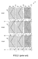
- each pixel 10 has two red sub-pixel segments 12a, 12b; two green sub-pixel segments 14a, 14b; and two blue sub-pixel segments 16a, 16b on the same row. While one sub-pixel segment is selected or turned on by a gate-line signal in one gate line, the other sub-pixel segment is selected or turned on by the combination of gate line signals in two gate lines. As illustrated in Figure 2 , the sub-pixel segment 12b is selected by the gate line signal in gate line G1 on Row 1, whereas the sub-pixel segment 12a is selected by the combination of the gate line signal in gate line G1 and the gate line signal in gate line G2 in Row 2.
- the data lines D1, D2, D3 provide data signals only to sub-pixel segments 12b, 14b and 16b .
- the electrode of the sub-pixel segment 12a in a row is connected to the electrode of the sub-pixel segment 12b in the next row.
- the electrode of the sub-pixel segment 14a in a row is connected to the electrode of the sub-pixel segment 14b in the next row.
- the electrode of the sub-pixel segment 16a in a row is connected to the electrode of the sub-pixel segment 16b in the next row.
- the gate line signal in each gate line includes a front-pulse and a rear pulse as shown in Figure 3 .
- the rear pulse is two times longer than the front pulse.
- the front pulse in gate line G2 occurs in the first half of the rear pulse in gate line G1.
- the front pulse in gate line G3 in Row 3 occurs in the first half of the rear pulse in gate line G2, and so on.
- the special waveform in the data signals in data lines D1, D2, etc. is designed to improve the visual effect, known as color washout, in a liquid crystal display.
- the arrangement of the sub-pixel segments and the control transistors is known as a multi-switch architecture
- the present invention provides a gate driver and a method for making same.
- the gate driver is used for providing gate-lines signals in the gate-lines in a liquid crystal display (LCD) panel.
- the gate-line signal in each gate line includes a front-pulse and a rear pulse.
- the gate line signals are particular useful in an LCD panel using a multi-switch architecture.
- the present invention uses a gate-on-array (GOA) circuit to implement the multi-switch waveform, for example.
- GAA gate-on-array
- the first aspect of the present invention is an electronic circuit for generating a signal pulse comprising a front pulse and a rear pulse in a non-overlapping manner in reference to a reference signal, the circuit comprising:
- the front-pulse generating part further comprises:
- the rear-pulse generating part further comprises:
- the front pulse has a pulse length equal to a clock period, the front pulse having a leading edge, and the front start pulse has a first edge leading a second edge, and wherein the leading edge of the front pulse is behind the first edge of the front start pulse by two pulse lengths, and the rear pulse has a leading edge and the rear start pulse has a first edge leading a second edge, wherein the first edge of the rear start pulse is behind the first edge of the front start pulse by two pulse lengths and the leading edge of the rear pulse is behind the first edge of the rear start pulse by two pulse lengths.
- the first pull-up circuit in the front-pulse generating part comprises a switching element having a control end operatively connected to a first switch end for receiving the front start pulse, and a second switch end for providing the first signal of the front-pulse generating part; and the first pull-up circuit in the rear-pulse generating part comprises a switching element having a control end operatively connected to a first switch end for receiving the rear start pulse, and a second switch end for providing the first signal of the front-pulse generating part.
- the second pull-up circuit in the front-pulse generating part comprises a switching element having a control end arranged to receive the first signal of the front-pulse generating part, a first switch end arranged to receive the first clock signals and the second switch end for providing the front pulse at a first node
- the second pull-up circuit in the rear-pulse generating part comprises a switching element having a control end arranged to receive the first signal of the rear-pulse generating part, a first switch end arranged to receive the second clock signals and the second switch end for providing the rear pulse at a second node, wherein the first node is operatively connected to the second node for providing the front pulse and the rear pulse.
- the first pull-down circuit in the front-pulse generating part comprises:
- the second pull-down circuit in the front-pulse generating part comprises a switching element having a control end arranged to receive the second signal of the front-pulse generating part, a first switch end connected to the first node and a second switch end arranged to receive the reference voltage; and the second pull-down circuit in the rear-pulse generating part comprises a switching element having a control end arranged to receive the second signal of the rear-pulse generating part, a first switch end connected to the second node and a second switch end arranged to receive the reference voltage.
- the front-pulse generating part further comprises a resetting circuit connected to the control end of the second pull-up circuit in the front-pulse generating part for causing the first signal of the front-pulse generating part to change from the first state to a different second state after the front-pulse is provided by the second pull-up circuit of the front-pulse generating part; and the rear-pulse generating part further comprises a resetting circuit connected to the control end of the second pull-up circuit in the rear-pulse generating part for causing the first signal of the rear-pulse generating part to change from the first state to a different second state after the rear-pulse is provided by the second pull-up circuit of the rear-pulse generating part.
- the first signal of the front-pulse generating part when the first signal of the front-pulse generating part is in the second state, the first signal has a voltage level equal to the reference voltage, when the first signal of the front-pulse generating part is in the first state, the first signal has a voltage level higher than the reference voltage, when the first signal of the rear-pulse generating part is in the second state, the first signal has a voltage level equal to the reference voltage, and when the first signal of the rear-pulse generating part is in the first state, the first signal has a voltage level higher than the reference voltage.
- the switching elements are n-MOS transistors with the control end of the switching element being the gate terminal of the transistor. Accordingly, the first state is a HIGH state and the second state is a LOW state.
- the switching elements are p-MOS transistors. Accordingly, the first state is a LOW state and the second state is a HIGH state.
- the second aspect of the present invention is a gate driver for use in a liquid crystal display, the liquid crystal display comprising a plurality of pixels arranged in a plurality of rows, the gate driver comprising a plurality of the gate-line generating circuits connected in series, each of gate-line generating circuits arranged to provide a gate signal pulse to each of the plurality of rows, wherein the gate-line generating circuits comprises a first-stage circuit, a second-stage circuit and a third-stage circuit, and wherein each of the gate-line generating circuits comprises an electronic device as described above.
- the gate driver is connected to a timing control, such that the first-stage circuit is arranged to receive the front start pulse and the rear start pulse from the timing control, and the timing control comprises:
- the third aspect of the present invention is a liquid crystal display comprising a plurality of pixels arranged in a plurality of rows, the display comprising:
- the fourth aspect of the present invention is a method for generating gate-line signals, each gate-line signals having a front pulse and a rear pulse.
- the method comprises:
- the required gate-line signal to select or turn on a pixel row for each frame time comprises a front-pulse and a rear-pulse.
- the length of the front-pulse is measured in a time unit T and the length of the rear-pulse is equal to 2T, with a separation of T between the front and rear pulses.
- the front-pulse of a gate line signal in a gate line occurs at the first half of the rear-pulse of a gate line signal in a preceding gate line.
- the present invention provides a gate driver having a series of shift registers, wherein each shifter register provides the gate line signals to a gate line.
- the gate driver 300 comprises a series of shift registers (SRs) to provide a series of gate line signals in sequential stages, and a timing-control module 30 to control the timing of the shift registers.
- SRs shift registers
- Each shift register 40 has four clock inputs CK1, CK2, XCK2 and CK3 for receiving clock pulses from the timing control module 30 , two start pulse inputs IN1, IN2; one output OUT to provide the gate line signals in one gate line; two carry pulse outputs X1, X2 for providing start pulses to the shift register in the next stage and for providing feedback pulses to the shift register in the previous stage; and two feedback inputs F1, F2 to receive the feedback pulses from the shift register in the next stage.
- the shift registers are connected in series in order to provide a series of gate line signals to a plurality of gate lines in sequential stages, only the start pulse inputs IN1, IN2 of the shift register in the first stage receive the start pulses ST1, ST2 from the timing control module 30 .
- the start pulse inputs IN1, IN2 in each of the shift registers in the subsequent stages receive the start pulses from the carry pulse outputs X1, X2 of the shifter register in the preceding stage.
- the length of the front-pulse is measured in a time unit T and the length of the rear-pulse is equal to 2T, with a separation of T between the front and rear pulses.
- the length of the start pulse ST1 is T, and the cycle of the start pulse ST1 is related to a frame time.
- the clock pulse CK1 has a cycle of 4T and the first clock pulse to start the shift register chain is 2T behind the start pulse ST1.
- the front-pulse in the gate line signals in the first gate line (G1) is in sync with the first clock pulse CK1 after the start pulse
- the front-pulse in the gate line signals in the second gate line (G2) is 2T behind the front-pulse in G1.
- a different clock pulse SCK1 is used to provide the clock pulse CK1 in the second, fourth and other even-numbered shift registers in the chain, wherein the clock pulse SCK1 also has a length of T and is 2T behind CK1.
- the rear-pulse in the gate line signals has a length of 2T and is separated from the front-pulse by T.
- the rear-pulse in the first gate line (G1) is in sync with the clock pulse CK3.
- the clock pulse CK3 is separated from the clock pulse CK1 by T.
- the rear-pulse of the second gate line (G2) occurs after the rear-pulse in G1.
- clock pulse CK3 of the first, third, fifth and other odd-numbered shift registers in the chain is provided by the CK3 output of the timing control module 30
- a different clock pulse XCK3 is provided to the clock pulse input CK3 of the second, fourth and other even-numbered shift registers in the chain, wherein the phase of clock pulse XCK3 is complementary to the phase of the clock pulse CK3.
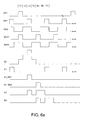
- the timing of clock pulse CK2 is related to CK1. As shown in Figure 6a , CK2 has a length of 2T and is T ahead of CK1. Thus, while the clock pulse CK2 of the first, third, fifth and other odd-numbered shift registers in the chain is provided by the CK2 output of the timing control module 30 , a different clock pulse XCK2 is provided to the clock pulse input CK2 of the second, fourth and other even-numbered shift registers in the chain, wherein the phase of clock pulse XCK2 is complementary to the phase of the clock pulse CK2.
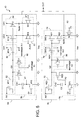
- the shift register 40 is shown in Figure 5 .
- the shift register 40 has two parts, a front-pulse generating part 50 and a rear-pulse generating part 70 . They are linked together at Node 1 and Node 2 to produce the gate line signals.
- the front-pulse generating part 50 has a first pull-up driving circuit 52 for providing an output Q1 in response to a start pulse (ST1 for the first shift register) received at start pulse input IN1.
- the first pull-up driving circuit 52 comprises a switching element or TFT M11, with its gate terminal connected to its source terminal. As shown in the timing chart of Figure 6a , the start pulse ST1 occurs during T1.
- the output Q1 is connected to a first pull-down circuit 58 such that the output Q1 is pulled down if the TFT M16 is in a conducting state, or P1 is high.
- P1 is substantially the same as the voltage level at the clock pulse input CK1 only when the TFT M15 is a non-conducting state or Q1 is low. But when Q1 is high, P1 is always low and TFT M16 is in a non-conducting state. This means the first pull-down driving circuit 58 does not pull down Q1.
- the first pull-down driving circuit 58 is also used to provide a signal P1 to a second pull-down circuit 62 .
- Q1 is only reset by a feedback circuit 60 .
- the output Q1 is provided to the gate terminals of a number of switching elements in a parallel pull-up circuit 54 and a carry buffer 56 .
- the carry buffer 56 comprises a TFT M14 with its source terminal connected to the first clock pulse CK1, and its gate terminal connected to Q1.
- the drain of TFT M14 is used to provide a start pulse X1 to the start pulse input IN1 of the shift register in the immediately following stage. Since M14 is in a conducting state after the first pull-up driving circuit 52 receives a start pulse ST1, the output at terminal X1 is in sync with the clock pulse CK1 after the start pulse ST1.
- the output X1 is shown as X1_SR1 in the timing chart of Figure 6a . As shown in Figure 6a , the clock pulse CK1 immediately following the start pulse ST1 occurs during T3, and X1_SR1 also occurs during T3. It should be noted that the signal X1_SR1 is provided as a start pulse in the front-pulse generating part in the next shift register.
- the parallel pull-up circuit 54 comprises a TFT M12 and a TFT M13 connected in parallel in that their gate terminals are connected together to receive the output Q1 from the first pull-up driving circuit 52 .
- the source terminal of TFT M12 is configured to receive signals from the clock pulse input CK1 and the source terminal of TFT M13 is configured to receive signals from the clock pulse input CK2.
- the drain terminals of TFT M12 and TFT M13 are connected to the second pull-down driving circuit 62 .
- the second pull-down driving circuit 62 comprises a TFT M19 connected in series to M12 in the parallel pull-up circuit 54 .
- the gate terminal of TFT M19 is connected to the output P1 of the TFT M15 in the first pull-down driving circuit 58 . Since TFT M12 is in a conducting state after the first pull-up driving circuit 52 receives a start pulse ST1, the output at Node 1 is in sync with the clock pulse CK1 after the start pulse ST1 when TFT M19 is non-conducting.
- the output at Node 1 provides the front-pulse in the gate line signals G1 as shown in the timing chart of Figure 6a .
- the front-pulse in the gate line signals G1 occurs during T3.
- the TFT M11 in the first pull-up driving circuit 52 is conducting only when it receives the start pulse ST1 during T1. After the start pulse ST1 has passed, TFT M11 is non-conducting and Q1 is in a floating state.
- the voltage level of Q1 is affected by the voltage level of CK2 and the voltage level of CK1 via coupling through the parasitic capacitance in TFT M13 and TFT M12.
- CK2 is high and CK1 is low during T2
- the voltage level of Q1 is boosted up.
- both CK1 and CK2 are high, and the voltage level of Q1 is further increased.
- both CK1 and CK2 are low, the voltage level of Q1 resumes the voltage level during T1 until Q1 is reset by the feedback circuit 60 by the next stage X1, or X1_SR2.
- X1 of the current stage or X1_SR1 occurs in sync with the clock pulse CK1 immediately after the start pulse ST1.
- the start pulse ST1 occurs during T1 and X1_SR1 occurs during T3.
- the clock input to M12 of the parallel pull up circuit 54 and the capacitor C1 in the first pull-down driving circuit 58 is SCK1, and not CK1.
- the next stage X1 (X1_SR2) is in sync with the clock pulse SCK1 immediately after the start pulse (X1_SR1) received by the next stage.
- X1_SR2 occurs during T5.
- Q1 of the current stage is reset by X1_SR2 at T5 and remains reset until the next start pulse for the next frame or picture.
- the rear-pulse generating part 70 has a first pull-up driving circuit 72 for providing an output Q2 in response to a start pulse (ST2 for the first shift register) received at start pulse input IN2 during the period of T34 as shown in Figure 6b .
- the first pull-up driving circuit 72 comprises a switching element or TFT M21, with its gate terminal connected to its source terminal.
- the output Q2 is connected to a first pull-down driving circuit 78 such that the output Q2 is pulled down if the TFT M26 is in a conducting state, or P2 is high.
- P2 is substantially the same as the voltage level at the clock pulse input CK3 only when the TFT M25 is in a non-conducting state or Q2 is low. But when Q2 is high, P2 is always low and TFT M26 is in a non-conducting state. This means the first pull down driving circuit 78 does not pull down Q2.
- the first pull down driving circuit 78 is used to provide a signal P2 to a second pull-down circuit 82 .
- Q2 is only reset by a feedback circuit 80 .
- the output Q2 is provided to the gate terminals of a number of switching elements in a series pull-up circuit 74 and a carry buffer 76 .
- the carry buffer 76 comprises a TFT M24 with its source terminal connected to the clock pulse CK3, and its gate terminal connected to Q2.
- the drain of TFT M24 is used to provide a start pulse to the start pulse input IN2 of the shift register in a following stage. Since M24 is in a conducting state after the first pull-up driving circuit 72 receives a start pulse ST2, the output at terminal X2 is in sync with the third clock pulse CK3 after the start pulse ST2. The output X2 is in sync with the clock pulse CK3 after the start pulse ST2.
- the output X2 is shown as X2_SR1 in the timing chart of Figure 6b .
- the clock pulse CK3 immediately follows the start pulse ST2 occurs at T56, and X2_SR1 also occurs at T56. It should be noted that the signal X2_SR1 is provided as a start pulse to the rear-pulse generating part 70 in the next register.
- the series pull-up circuit 74 comprises a TFT M22 and a TFT M23 connected in series and their gate terminals are connected together to receive the output Q2 from the first pull-up driving circuit 72 .
- the source terminal of TFT M22 is configured to receive signals from the clock pulse input CK3 and the source terminal of TFT M23 is connected to the drain terminal of TFT M22.
- the drain terminal of TFT M23 is connected to the second pull-down driving circuit 82 .
- the source terminal of TFT M22 is configured to receive signals from the clock signal CK3.
- the drain terminal of TFT M23 is connected to the second pull down driving circuit 82 .
- the second pull-down driving circuit 82 comprises a TFT M28 connected in series to M23 in the series pull-up circuit 74 .
- the gate terminal of TFT M28 is connected to the output P2 of the TFT M25 in the first pull-down driving circuit 78 . Since TFT M22 and TFT M23 are in a conducting state after the first pull up driving circuit 72 receives a start pulse ST2, the output at Node 2 is in sync with the clock pulse CK3 after the start pulse ST2 when TFT M28 is non-conducting.
- the output at Node 2 provides the rear-pulse in the gate line signals G1 as shown in the timing chart of Figure 6a and 6b .
- the rear-pulse in the gate line signals G1 occurs at T56, which is corresponding to the time periods T5 and T6 in Figure 6a .
- the TFT M21 in the first pull up driving circuit is conducting only when it receives the start pulse ST2 during T34. After the start pulse ST2 has passed, TFT M21 is non-conducting and Q2 is in a floating state.
- the voltage level of Q2 is affected by the voltage level of CK3 via coupling through the parasitic capacitance in TFT M22 and TFT M23. Thus, when CK3 is high during T56, the voltage level of Q2 is boosted up. Afterwards, Q2 is reset by the feedback circuit 80 by the next stage X2 or X2_SR2.
- X2 of the current stage or X2_SR1 occurs in sync with the clock pulse CK3 immediately after the start pulse ST2.
- the start pulse ST2 occurs during T34 and X2_SR1 occurs during T56.
- the clock input to the series pull up circuit 74 and the capacitor C2 in the first pull down driving circuit 78 is XCK3, and not CK3.
- the next stage X2 (X2_SR2) is in sync with the clock pulse XCK3 immediately after the start pulse (X2_SR1) for the next stage.
- X2_SR2 occurs during T78.
- Q2 of the current stage is reset by X2_SR2 at T78 and remains reset until the next start pulse of the next frame or picture.
- the front pulse X1 of the current stage (X1_SR1) is generated at Node 1 by CK1 at the parallel pull-up circuit 54 conditioned by P1 output of the second pull-down driving circuit 62 .
- P1 is kept LOW by the first pull-down driving circuit 58 when Q1 is HIGH.
- Q1 is caused to become HIGH by the start pulse ST1 (or IN1) at the first pull-up driving circuit 52 and is kept in the HIGH state by CK2 and CK1 at the parallel pull-up circuit 54 .
- Q1 is reset by the next-stage front pulse X1.
- the rear pulse X2 of the current stage (X2_SR1) is generated at Node 2 by CK3 at the series pull-up circuit 74 conditioned by P2 output of the second pull-down driving circuit 82 .
- P2 is kept LOW by the first pull-down driving circuit 78 when Q2 is HIGH.
- Q2 is caused to become HIGH by the start pulse ST2 (or IN2) at the first pull-up driving circuit 70 and is kept in the HIGH state by CK3 at the series pull-up circuit 74 .
- Q2 is reset by the next-stage front pulse X2.
- the front-pulse generating part 50 uses a first pull-up driving circuit 52 to provide a first signal Q1 in order to pull down a second signal P1 in a first pull-down circuit 58 . While P1 is pulled down, a first start pulse CK1 is used to provide a front pulse X1 from the second pull-up circuit 54 .
- the rear-pulse generating part 70 uses a first pull-up driving circuit 72 to provide a first signal Q2 in order to pull down a second signal P2 in a first pull down circuit 78 . While P2 is pulled-down, a second start pulse CK3 is used to provide a rear pulse X2 at the second (series) pull-up circuit 74 .
- the present invention provides a gate driver and a method for making same.
- the gate driver is used for providing gate-lines signals in the gate-lines in a liquid crystal display (LCD) panel.
- the gate-line signal in each gate line includes a front-pulse and a rear pulse.
- the gate line signals are particular useful in an LCD panel using a multi-switch architecture.
- the present invention uses a gate-on-array (GOA) circuit to implement the multi-switch waveform, for example.
- GAA gate-on-array
- the method of generating gate-line signals comprises:
- the gate driver comprises a plurality of shift registers connected in series, each shift register is arranged for generating a gate-line signal having a front pulse and a rear pulse in a non-overlapping manner in reference to a reference signal, such as Vss.
- the shift register comprises a front-pulse generating part for generating the front pulse; and a rear-pulse generating part for generating the rear pulse, wherein the front-pulse generating part is configured to receive a front start pulse and a series of first clock signals, the front-pulse generating part comprising:
- the front-pulse generating part further comprises:
- the front pulse has a pulse length equal to a clock period, the front pulse having a leading edge, and the front start pulse has a first edge leading a second edge, and wherein the leading edge of the front pulse is behind the first edge of the front start pulse by two pulse lengths, and the rear pulse has a leading edge and the rear start pulse has a first edge leading a second edge, wherein the first edge of the rear start pulse is behind the first edge of the front start pulse by two pulse lengths and the leading edge of the rear pulse is behind the first edge of the rear start pulse by two pulse lengths.
- the first pull-up circuit in the front-pulse generating part comprises a transistor having a gate terminal operatively connected to the source terminal for receiving the front start pulse, and a drain terminal for providing the first signal of the front-pulse generating part; and wherein the first pull-up circuit in the rear-pulse generating part comprises a transistor having a gate terminal connected to the source terminal for receiving the rear start pulse, and the drain terminal arranged for providing the first signal of the front-pulse generating part.
- the second pull-up circuit in the front-pulse generating part comprises a transistor having a gate terminal arranged to receive the first signal of the front-pulse generating part, a source terminal arranged to receive the first clock signals and the drain terminal arranged for providing the front pulse at a first node
- the second pull-up circuit in the rear-pulse generating part comprises a transistor having a gate terminal arranged to receive the first signal of the rear-pulse generating part, a source terminal arranged to receive the second clock signals and a drain terminal for providing the rear pulse at a second node, wherein the first node is operatively connected to the second node for providing the front pulse and the rear pulse.
- the first pull-down circuit in the front-pulse generating part and the rear-pulse generating part comprises:
- the second pull-down circuit in the front-pulse generating part and the rear-pulse generating part comprises a transistor having a gate terminal arranged to receive the second signal of the corresponding pulse generating part, a source terminal connected to the output of the shift register and a drain terminal arranged to receive the reference voltage.
- Each of the front-pulse generating part and the rear-pulse generating part further comprises a resetting circuit connected to the control end of the second pull-up circuit in the corresponding pulse generating part for causing the first signal of the corresponding pulse generating part to change from the first state to a different second state after the front-pulse or rear pulse is provided by the second pull-up circuit of the corresponding pulse generating part.
- the gate driver is connected to a timing control, such that the first-stage circuit is arranged to receive the front start pulse and the rear start pulse from the timing control, and wherein the timing control comprises:
- Each shift register has a front carry buffer circuit for providing front start pulse to the next-stage shift register, and a rear carry buffer circuit for providing the rear start pulse to the next-stage shift register.
- the transistors can be n-MOS transistors or p-MOS transistors.
- the first state of the first signal is HIGH and the second state is LOW for n-MOS transistors.
- the first state of the first signal is LOW and the second state is HIGH for p-MOS transistors.
- the carry buffer 56 is connected to the parallel pull-up circuit 54 in parallel so that the TFT M14 in the carry buffer 56 and the TMT M12 in the parallel pull-up circuit 54 are simultaneously in the conducting state when Q1 is high.
- the clock pulse CK1 can be used as the front start pulse for the next-stage shift register.
- the front pulse X1_SR1 itself can also be used as the front start pulse IN1 for the next-stage shift register.
- the rear pulse X2_SR1in the rear pulse generating part in the current stage can also be used as the rear start pulse IN2 for the next-stage shift register.
Landscapes
- Engineering & Computer Science (AREA)
- Chemical & Material Sciences (AREA)
- Crystallography & Structural Chemistry (AREA)
- Physics & Mathematics (AREA)
- Computer Hardware Design (AREA)
- General Physics & Mathematics (AREA)
- Theoretical Computer Science (AREA)
- Control Of Indicators Other Than Cathode Ray Tubes (AREA)
- Liquid Crystal Display Device Control (AREA)
- Shift Register Type Memory (AREA)
- Liquid Crystal (AREA)
- Electronic Switches (AREA)
Abstract
Description
- The present invention relates generally to a gate driver for use in a liquid crystal display and, more particularly, to a gate driver circuit having a series of shift registers.
- As known in the art, a color liquid crystal display (LCD)
panel 1 has a two-dimensional array ofpixels 10, as shown inFigure 1 . Each of the pixels comprises a plurality of sub-pixels, usually in three primary colors of red (R), green (G) and blue (B). These RGB color components can be achieved by using respective color filters. The array ofpixels 10 is organized in rows and columns and a plurality of gate lines are used to select or activate the pixels in the rows and a plurality of data lines are used to provide data to the pixels in the columns. Thus, theLCD panel 1 generally has agate driver 300 to provide gate-line signals in the gate-lines and adata driver 200 to provide data signals to the data lines. - In some LCD panels, each color sub-pixel has two sub-pixel segments. As shown in
Figure 2 , eachpixel 10 has twored sub-pixel segments green sub-pixel segments blue sub-pixel segments Figure 2 , thesub-pixel segment 12b is selected by the gate line signal in gate line G1 onRow 1, whereas thesub-pixel segment 12a is selected by the combination of the gate line signal in gate line G1 and the gate line signal in gate line G2 inRow 2. The data lines D1, D2, D3 provide data signals only tosub-pixel segments sub-pixel segment 12a in a row is connected to the electrode of thesub-pixel segment 12b in the next row. The electrode of thesub-pixel segment 14a in a row is connected to the electrode of thesub-pixel segment 14b in the next row. The electrode of thesub-pixel segment 16a in a row is connected to the electrode of thesub-pixel segment 16b in the next row. - In such an LCD panel, the gate line signal in each gate line includes a front-pulse and a rear pulse as shown in
Figure 3 . - As shown in
Figure 3 , the rear pulse is two times longer than the front pulse. The front pulse in gate line G2 occurs in the first half of the rear pulse in gate line G1. The front pulse in gate line G3 in Row 3 occurs in the first half of the rear pulse in gate line G2, and so on. The special waveform in the data signals in data lines D1, D2, etc. is designed to improve the visual effect, known as color washout, in a liquid crystal display. The arrangement of the sub-pixel segments and the control transistors is known as a multi-switch architecture - The present invention provides a gate driver and a method for making same. The gate driver is used for providing gate-lines signals in the gate-lines in a liquid crystal display (LCD) panel. In particular, the gate-line signal in each gate line includes a front-pulse and a rear pulse. The gate line signals are particular useful in an LCD panel using a multi-switch architecture. The present invention uses a gate-on-array (GOA) circuit to implement the multi-switch waveform, for example.
- Thus, the first aspect of the present invention is an electronic circuit for generating a signal pulse comprising a front pulse and a rear pulse in a non-overlapping manner in reference to a reference signal, the circuit comprising:
- a front-pulse generating part for generating the front pulse; and
- a rear-pulse generating part for generating the rear pulse, wherein
- the front-pulse generating part is configured to receive a front start pulse and a series of first clock signals, the front-pulse generating part comprising:
- a first pull-up circuit for providing a first signal in a first state in reference to the reference voltage in response to the front start pulse;
- a second pull-up circuit to at least maintain the first signal in the first state; and
- a first pull-down circuit for providing a second signal in response to the first signal, wherein the second signal is in a pulled-down state in reference to the reference voltage when the first signal is in the first state, and wherein the second pull-up circuit is further configured to receive the first clock signals in order to provide the front pulse in response to the first clock signals while the second signal is in the pulled-down state; and wherein
- the rear-pulse generating part is configured to receive a rear start pulse and a series of second clock signals, the rear-pulse generating part comprising:
- a first pull-up circuit for providing a first signal in a first state in reference to the reference voltage in response to the rear start pulse;
- a second pull-up circuit to at least maintain the first signal in the first state; and
- a first pull-down circuit for providing a second signal in response to the first signal, wherein the second signal is in a pulled-down state in reference to the reference voltage when the first signal is in the first state, and wherein the second pull-up circuit is further configured to receive the second clock signals in order to provide the rear pulse in response to the second clock signals while the second signal is in the pulled down state.
- The front-pulse generating part further comprises:
- a second pull-down circuit configured to receive the second signal of the front-pulse generating part, wherein the pull-up circuit is connected to the second pull-down circuit in series such that the front pulse is provided in response to the first clock signals only when the second signal is in the pull-down state.
- The rear-pulse generating part further comprises:
- a second pull-down circuit configured to receive the second signal of the rear-pulse generating part, wherein the pull-up circuit is connected to the second pull-down circuit in series such that the rear pulse is provided in response to the second clock signals only when the second signal is in the pull-down state.
- According to the present invention, the front pulse has a pulse length equal to a clock period, the front pulse having a leading edge, and the front start pulse has a first edge leading a second edge, and wherein the leading edge of the front pulse is behind the first edge of the front start pulse by two pulse lengths, and
the rear pulse has a leading edge and the rear start pulse has a first edge leading a second edge, wherein the first edge of the rear start pulse is behind the first edge of the front start pulse by two pulse lengths and the leading edge of the rear pulse is behind the first edge of the rear start pulse by two pulse lengths. - According to the present invention, the first pull-up circuit in the front-pulse generating part comprises a switching element having a control end operatively connected to a first switch end for receiving the front start pulse, and a second switch end for providing the first signal of the front-pulse generating part; and the first pull-up circuit in the rear-pulse generating part comprises a switching element having a control end operatively connected to a first switch end for receiving the rear start pulse, and a second switch end for providing the first signal of the front-pulse generating part.
- According to the present invention, the second pull-up circuit in the front-pulse generating part comprises a switching element having a control end arranged to receive the first signal of the front-pulse generating part, a first switch end arranged to receive the first clock signals and the second switch end for providing the front pulse at a first node, and wherein
the second pull-up circuit in the rear-pulse generating part comprises a switching element having a control end arranged to receive the first signal of the rear-pulse generating part, a first switch end arranged to receive the second clock signals and the second switch end for providing the rear pulse at a second node, wherein the first node is operatively connected to the second node for providing the front pulse and the rear pulse. - According to the present invention, the first pull-down circuit in the front-pulse generating part comprises:
- a capacitor having a first capacitor end arranged to receive the first clock signals, and a second capacitor end;
- a first switching element having a control end connected to the second capacitor end, a first switch end arranged to receive the first signal of the front-pulse generating part, and a second switch end arranged to receive the reference voltage; and
- a second switching element having a control end arranged to receive the first signal of the front-pulse generating part, a first switch end connected to the second capacitor end, and a second switch end arranged to receive the reference voltage, and wherein
- a capacitor having a first capacitor end arranged to receive the second clock signals, and a second capacitor end;
- a first switching element having a control end connected to the second capacitor end, a first switch end arranged to receive the first signal of the rear-pulse generating part, and a second switch end arranged to receive the reference voltage, and
- a second switching element having a control end arranged to receive the first signal of the rear-pulse generating part, a first switch end connected to the second capacitor end, and a second switch end arranged to receive the reference voltage.
- According to the present invention, the second pull-down circuit in the front-pulse generating part comprises a switching element having a control end arranged to receive the second signal of the front-pulse generating part, a first switch end connected to the first node and a second switch end arranged to receive the reference voltage; and the second pull-down circuit in the rear-pulse generating part comprises a switching element having a control end arranged to receive the second signal of the rear-pulse generating part, a first switch end connected to the second node and a second switch end arranged to receive the reference voltage.
- According to the present invention, the front-pulse generating part further comprises a resetting circuit connected to the control end of the second pull-up circuit in the front-pulse generating part for causing the first signal of the front-pulse generating part to change from the first state to a different second state after the front-pulse is provided by the second pull-up circuit of the front-pulse generating part; and the rear-pulse generating part further comprises a resetting circuit connected to the control end of the second pull-up circuit in the rear-pulse generating part for causing the first signal of the rear-pulse generating part to change from the first state to a different second state after the rear-pulse is provided by the second pull-up circuit of the rear-pulse generating part.
- According to the present invention, when the first signal of the front-pulse generating part is in the second state, the first signal has a voltage level equal to the reference voltage, when the first signal of the front-pulse generating part is in the first state, the first signal has a voltage level higher than the reference voltage, when the first signal of the rear-pulse generating part is in the second state, the first signal has a voltage level equal to the reference voltage, and when the first signal of the rear-pulse generating part is in the first state, the first signal has a voltage level higher than the reference voltage.
- In the electronic device, according to the present invention, the switching elements are n-MOS transistors with the control end of the switching element being the gate terminal of the transistor. Accordingly, the first state is a HIGH state and the second state is a LOW state.
- In a different embodiment, the switching elements are p-MOS transistors. Accordingly, the first state is a LOW state and the second state is a HIGH state.
- The second aspect of the present invention is a gate driver for use in a liquid crystal display, the liquid crystal display comprising a plurality of pixels arranged in a plurality of rows, the gate driver comprising a plurality of the gate-line generating circuits connected in series, each of gate-line generating circuits arranged to provide a gate signal pulse to each of the plurality of rows, wherein the gate-line generating circuits comprises a first-stage circuit, a second-stage circuit and a third-stage circuit, and wherein each of the gate-line generating circuits comprises an electronic device as described above.
- According to the present invention, the gate driver is connected to a timing control, such that the first-stage circuit is arranged to receive the front start pulse and the rear start pulse from the timing control, and the timing control comprises:
- a first pulse output for providing first pulse signals;
- a second pulse output for providing second pulse signals having complementary phase relation with the first pulse signals;
- a third pulse output for providing third pulse signals; and
- a fourth pulse output for providing fourth pulse signals having complementary phase relation with the third pulse signals; and wherein
- the first-stage circuit is arranged to receive the first pulse signals for providing the first clock signals in the electronic device in the first-stage circuit and the third pulse signals for providing the second clock signals in the electronic device in the first-stage circuit, the first-stage circuit further comprising:
- a first front carry buffer circuit comprising a switching element having a control end arranged to receive the first signal in the corresponding front-pulse generating part, a first switch end arranged to receive the first clock signals and a second switch end for providing the front start pulse to the second-stage circuit, and
- a first rear carry buffer circuit comprising a switching element having a control end arranged to receive the first signal in the corresponding rear-pulse generating part, a first switch end arranged to receive the second clock signals and a second switch end for providing the rear start pulse to the second-stage circuit;
- the second-stage circuit is arranged to receive the second pulse signals for providing the first clock signals in the electronic device in the second-stage circuit and the fourth pulse signals for providing the second clock signals in the electronic device in the second-stage circuit, the second-stage circuit further comprising:
- a second front carry buffer circuit comprising a switching element having a control end arranged to receive the first signal in the corresponding front-pulse generating part, a first switch end arranged to receive the first clock signals and a second switch end for providing the front start pulse to the third-stage circuit, and
- a second rear carry buffer circuit comprising a switching element having a control end arranged to receive the first signal in the corresponding rear-pulse generating part, a first switch end arranged to receive the second clock signals and a second switch end for providing the rear start pulse to the third-stage circuit; and
- the third-stage circuit is arranged to receive the first pulse signals for providing the first clock signals in the electronic device in the third-stage circuit and the third pulse signals for providing the second clock signals in the electronic device in the third-stage circuit, the first-stage circuit further comprising:
- a first front carry buffer circuit comprising a switching element having a control end arranged to receive the first signal in the corresponding front-pulse generating part, a first switch end arranged to receive the first clock signals and a second switch end for providing the front start pulse to a fourth-stage circuit, and
- a first rear carry buffer circuit comprising a switching element having a control end arranged to receive the first signal in the corresponding rear-pulse generating part, a first switch end arranged to receive the second clock signals and a second switch end for providing the rear start pulse to a fourth-stage circuit.
- The third aspect of the present invention is a liquid crystal display comprising a plurality of pixels arranged in a plurality of rows, the display comprising:
- a gate driver comprising a plurality of the gate-line generating circuits connected in series, each of gate-line generating circuits arranged to provide a gate signal pulse to each of the plurality of rows, wherein each of the gate-line generating circuits comprises an electronic device as described above.
- The fourth aspect of the present invention is a method for generating gate-line signals, each gate-line signals having a front pulse and a rear pulse. The method comprises:
- providing a front start pulse;
- generating a first front signal in a first state in reference to the reference voltage in response to the front start pulse,
- generating a second front signal in response to the first front signal, wherein the second front signal is in a pulled-down state in reference to the reference voltage when the first front signal is in the first state,
- receiving a first clock signal for provide the front pulse while the second front signal is in the pulled-down state;
- providing a rear start pulse;
- generating a first rear signal in the first state in response to the rear start pulse,
- generating a second rear signal in response to the first rear signal, wherein the second rear signal is in a pulled-down state in reference to the reference voltage when the first rear signal is in the first state;
- receiving a second clock signal for provide the rear pulse while the second rear signal is in the pulled-down state;
- causing the first front signal to change from the first state to a second state after the front pulse is provided; and
- causing the first rear signal to change from the first state to a second state after the rear pulse is provided
- The present invention will become apparent upon reading the description taken in conjunction with
Figures 4-6b . -
-
Figure 1 shows a typical liquid crystal display. -
Figure 2 shows the sub-pixel segments and the control transistors according to gate-on-array technology. -
Figure 3 is a timing chart showing the signal waveforms in gate lines and data lines. -
Figure 4 shows a series of shift registers connected in a cascade fashion to provide the gate line signals, according to the present invention. -
Figure 5 shows a shift register circuit, according to the present invention. -
Figures 6a and6b show a timing chart for the signal waveforms in various signal lines, according to the present invention. - As seen in
Figure 3 , the required gate-line signal to select or turn on a pixel row for each frame time comprises a front-pulse and a rear-pulse. In one embodiment of the present invention, the length of the front-pulse is measured in a time unit T and the length of the rear-pulse is equal to 2T, with a separation of T between the front and rear pulses. Furthermore, the front-pulse of a gate line signal in a gate line occurs at the first half of the rear-pulse of a gate line signal in a preceding gate line. The present invention provides a gate driver having a series of shift registers, wherein each shifter register provides the gate line signals to a gate line. - The block diagram of the gate driver or generator, according to the present invention, is shown in
Figure 4 . As shown inFigure 4 , thegate driver 300 comprises a series of shift registers (SRs) to provide a series of gate line signals in sequential stages, and a timing-control module 30 to control the timing of the shift registers. Eachshift register 40 has four clock inputs CK1, CK2, XCK2 and CK3 for receiving clock pulses from thetiming control module 30, two start pulse inputs IN1, IN2; one output OUT to provide the gate line signals in one gate line; two carry pulse outputs X1, X2 for providing start pulses to the shift register in the next stage and for providing feedback pulses to the shift register in the previous stage; and two feedback inputs F1, F2 to receive the feedback pulses from the shift register in the next stage. When the shift registers are connected in series in order to provide a series of gate line signals to a plurality of gate lines in sequential stages, only the start pulse inputs IN1, IN2 of the shift register in the first stage receive the start pulses ST1, ST2 from thetiming control module 30. The start pulse inputs IN1, IN2 in each of the shift registers in the subsequent stages receive the start pulses from the carry pulse outputs X1, X2 of the shifter register in the preceding stage. - As can be seen from
Figures 6a and6b , the length of the front-pulse is measured in a time unit T and the length of the rear-pulse is equal to 2T, with a separation of T between the front and rear pulses. The length of the start pulse ST1 is T, and the cycle of the start pulse ST1 is related to a frame time. The clock pulse CK1 has a cycle of 4T and the first clock pulse to start the shift register chain is 2T behind the start pulse ST1. The front-pulse in the gate line signals in the first gate line (G1) is in sync with the first clock pulse CK1 after the start pulse, and the front-pulse in the gate line signals in the second gate line (G2) is 2T behind the front-pulse in G1. Thus, while the clock pulse CK1 of the first, third, fifth and other odd-numbered shift registers in the chain is provided by the CK1 output of thetiming control module 30, a different clock pulse SCK1 is used to provide the clock pulse CK1 in the second, fourth and other even-numbered shift registers in the chain, wherein the clock pulse SCK1 also has a length of T and is 2T behind CK1. - The rear-pulse in the gate line signals has a length of 2T and is separated from the front-pulse by T. The rear-pulse in the first gate line (G1) is in sync with the clock pulse CK3. Thus, the clock pulse CK3 is separated from the clock pulse CK1 by T. Furthermore, the rear-pulse of the second gate line (G2) occurs after the rear-pulse in G1. Thus, while the clock pulse CK3 of the first, third, fifth and other odd-numbered shift registers in the chain is provided by the CK3 output of the
timing control module 30, a different clock pulse XCK3 is provided to the clock pulse input CK3 of the second, fourth and other even-numbered shift registers in the chain, wherein the phase of clock pulse XCK3 is complementary to the phase of the clock pulse CK3. - The timing of clock pulse CK2 is related to CK1. As shown in
Figure 6a , CK2 has a length of 2T and is T ahead of CK1. Thus, while the clock pulse CK2 of the first, third, fifth and other odd-numbered shift registers in the chain is provided by the CK2 output of thetiming control module 30, a different clock pulse XCK2 is provided to the clock pulse input CK2 of the second, fourth and other even-numbered shift registers in the chain, wherein the phase of clock pulse XCK2 is complementary to the phase of the clock pulse CK2. - The
shift register 40, according to the present invention, is shown inFigure 5 . As shown inFigure 5 , theshift register 40 has two parts, a front-pulse generating part 50 and a rear-pulse generating part 70. They are linked together atNode 1 andNode 2 to produce the gate line signals. - The front-
pulse generating part 50 has a first pull-up drivingcircuit 52 for providing an output Q1 in response to a start pulse (ST1 for the first shift register) received at start pulse input IN1. The first pull-up drivingcircuit 52 comprises a switching element or TFT M11, with its gate terminal connected to its source terminal. As shown in the timing chart ofFigure 6a , the start pulse ST1 occurs during T1. - The output Q1 is connected to a first pull-
down circuit 58 such that the output Q1 is pulled down if the TFT M16 is in a conducting state, or P1 is high. P1 is substantially the same as the voltage level at the clock pulse input CK1 only when the TFT M15 is a non-conducting state or Q1 is low. But when Q1 is high, P1 is always low and TFT M16 is in a non-conducting state. This means the first pull-down drivingcircuit 58 does not pull down Q1. The first pull-down drivingcircuit 58 is also used to provide a signal P1 to a second pull-down circuit 62. Q1 is only reset by afeedback circuit 60. - The output Q1 is provided to the gate terminals of a number of switching elements in a parallel pull-up circuit 54 and a
carry buffer 56. - The
carry buffer 56 comprises a TFT M14 with its source terminal connected to the first clock pulse CK1, and its gate terminal connected to Q1. The drain of TFT M14 is used to provide a start pulse X1 to the start pulse input IN1 of the shift register in the immediately following stage. Since M14 is in a conducting state after the first pull-up drivingcircuit 52 receives a start pulse ST1, the output at terminal X1 is in sync with the clock pulse CK1 after the start pulse ST1. The output X1 is shown as X1_SR1 in the timing chart ofFigure 6a . As shown inFigure 6a , the clock pulse CK1 immediately following the start pulse ST1 occurs during T3, and X1_SR1 also occurs during T3. It should be noted that the signal X1_SR1 is provided as a start pulse in the front-pulse generating part in the next shift register. - The parallel pull-up circuit 54 comprises a TFT M12 and a TFT M13 connected in parallel in that their gate terminals are connected together to receive the output Q1 from the first pull-up driving
circuit 52. The source terminal of TFT M12 is configured to receive signals from the clock pulse input CK1 and the source terminal of TFT M13 is configured to receive signals from the clock pulse input CK2. The drain terminals of TFT M12 and TFT M13 are connected to the second pull-down drivingcircuit 62. - The second pull-down driving
circuit 62 comprises a TFT M19 connected in series to M12 in the parallel pull-up circuit 54. The gate terminal of TFT M19 is connected to the output P1 of the TFT M15 in the first pull-down drivingcircuit 58. Since TFT M12 is in a conducting state after the first pull-up drivingcircuit 52 receives a start pulse ST1, the output atNode 1 is in sync with the clock pulse CK1 after the start pulse ST1 when TFT M19 is non-conducting. The output atNode 1 provides the front-pulse in the gate line signals G1 as shown in the timing chart ofFigure 6a . Thus, the front-pulse in the gate line signals G1 occurs during T3. - The TFT M11 in the first pull-up driving
circuit 52 is conducting only when it receives the start pulse ST1 during T1. After the start pulse ST1 has passed, TFT M11 is non-conducting and Q1 is in a floating state. The voltage level of Q1 is affected by the voltage level of CK2 and the voltage level of CK1 via coupling through the parasitic capacitance in TFT M13 and TFT M12. Thus, when CK2 is high and CK1 is low during T2, the voltage level of Q1 is boosted up. During T3, both CK1 and CK2 are high, and the voltage level of Q1 is further increased. During T4, both CK1 and CK2 are low, the voltage level of Q1 resumes the voltage level during T1 until Q1 is reset by thefeedback circuit 60 by the next stage X1, or X1_SR2. - As shown in
Figure 6a , X1 of the current stage or X1_SR1 occurs in sync with the clock pulse CK1 immediately after the start pulse ST1. The start pulse ST1 occurs during T1 and X1_SR1 occurs during T3. It should be noted that, in the next register, the clock input to M12 of the parallel pull up circuit 54 and the capacitor C1 in the first pull-down drivingcircuit 58 is SCK1, and not CK1. Thus, the next stage X1 (X1_SR2) is in sync with the clock pulse SCK1 immediately after the start pulse (X1_SR1) received by the next stage. As shown inFigure 6a , X1_SR2 occurs during T5. Thus, Q1 of the current stage is reset by X1_SR2 at T5 and remains reset until the next start pulse for the next frame or picture. - The rear-
pulse generating part 70 has a first pull-up drivingcircuit 72 for providing an output Q2 in response to a start pulse (ST2 for the first shift register) received at start pulse input IN2 during the period of T34 as shown inFigure 6b . The first pull-up drivingcircuit 72 comprises a switching element or TFT M21, with its gate terminal connected to its source terminal. - The output Q2 is connected to a first pull-down driving
circuit 78 such that the output Q2 is pulled down if the TFT M26 is in a conducting state, or P2 is high. P2 is substantially the same as the voltage level at the clock pulse input CK3 only when the TFT M25 is in a non-conducting state or Q2 is low. But when Q2 is high, P2 is always low and TFT M26 is in a non-conducting state. This means the first pull down drivingcircuit 78 does not pull down Q2. The first pull down drivingcircuit 78 is used to provide a signal P2 to a second pull-down circuit 82. Q2 is only reset by afeedback circuit 80. - The output Q2 is provided to the gate terminals of a number of switching elements in a series pull-up
circuit 74 and acarry buffer 76. - The
carry buffer 76 comprises a TFT M24 with its source terminal connected to the clock pulse CK3, and its gate terminal connected to Q2. The drain of TFT M24 is used to provide a start pulse to the start pulse input IN2 of the shift register in a following stage. Since M24 is in a conducting state after the first pull-up drivingcircuit 72 receives a start pulse ST2, the output at terminal X2 is in sync with the third clock pulse CK3 after the start pulse ST2. The output X2 is in sync with the clock pulse CK3 after the start pulse ST2. The output X2 is shown as X2_SR1 in the timing chart ofFigure 6b . As shown inFigure 6b , the clock pulse CK3 immediately follows the start pulse ST2 occurs at T56, and X2_SR1 also occurs at T56. It should be noted that the signal X2_SR1 is provided as a start pulse to the rear-pulse generating part 70 in the next register. - The series pull-up
circuit 74 comprises a TFT M22 and a TFT M23 connected in series and their gate terminals are connected together to receive the output Q2 from the first pull-up drivingcircuit 72. The source terminal of TFT M22 is configured to receive signals from the clock pulse input CK3 and the source terminal of TFT M23 is connected to the drain terminal of TFT M22. The drain terminal of TFT M23 is connected to the second pull-down drivingcircuit 82. The source terminal of TFT M22 is configured to receive signals from the clock signal CK3. The drain terminal of TFT M23 is connected to the second pull down drivingcircuit 82. - The second pull-down driving
circuit 82 comprises a TFT M28 connected in series to M23 in the series pull-upcircuit 74. The gate terminal of TFT M28 is connected to the output P2 of the TFT M25 in the first pull-down drivingcircuit 78. Since TFT M22 and TFT M23 are in a conducting state after the first pull up drivingcircuit 72 receives a start pulse ST2, the output atNode 2 is in sync with the clock pulse CK3 after the start pulse ST2 when TFT M28 is non-conducting. The output atNode 2 provides the rear-pulse in the gate line signals G1 as shown in the timing chart ofFigure 6a and6b . Thus, the rear-pulse in the gate line signals G1 occurs at T56, which is corresponding to the time periods T5 and T6 inFigure 6a . - The TFT M21 in the first pull up driving circuit is conducting only when it receives the start pulse ST2 during T34. After the start pulse ST2 has passed, TFT M21 is non-conducting and Q2 is in a floating state. The voltage level of Q2 is affected by the voltage level of CK3 via coupling through the parasitic capacitance in TFT M22 and TFT M23. Thus, when CK3 is high during T56, the voltage level of Q2 is boosted up. Afterwards, Q2 is reset by the
feedback circuit 80 by the next stage X2 or X2_SR2. - As shown in
Figure 6b , X2 of the current stage or X2_SR1 occurs in sync with the clock pulse CK3 immediately after the start pulse ST2. The start pulse ST2 occurs during T34 and X2_SR1 occurs during T56. It should be noted that, in the next register, the clock input to the series pull upcircuit 74 and the capacitor C2 in the first pull down drivingcircuit 78 is XCK3, and not CK3. Thus, the next stage X2 (X2_SR2) is in sync with the clock pulse XCK3 immediately after the start pulse (X2_SR1) for the next stage. As shown inFigure 6b , X2_SR2 occurs during T78. Thus, Q2 of the current stage is reset by X2_SR2 at T78 and remains reset until the next start pulse of the next frame or picture. - In sum, the front pulse X1 of the current stage (X1_SR1) is generated at
Node 1 by CK1 at the parallel pull-up circuit 54 conditioned by P1 output of the second pull-down drivingcircuit 62. P1 is kept LOW by the first pull-down drivingcircuit 58 when Q1 is HIGH. Q1 is caused to become HIGH by the start pulse ST1 (or IN1) at the first pull-up drivingcircuit 52 and is kept in the HIGH state by CK2 and CK1 at the parallel pull-up circuit 54. Q1 is reset by the next-stage front pulse X1. - Likewise, the rear pulse X2 of the current stage (X2_SR1) is generated at
Node 2 by CK3 at the series pull-upcircuit 74 conditioned by P2 output of the second pull-down drivingcircuit 82. P2 is kept LOW by the first pull-down drivingcircuit 78 when Q2 is HIGH. Q2 is caused to become HIGH by the start pulse ST2 (or IN2) at the first pull-up drivingcircuit 70 and is kept in the HIGH state by CK3 at the series pull-upcircuit 74. Q2 is reset by the next-stage front pulse X2. - Thus, according to the present invention, the front-
pulse generating part 50 uses a first pull-up drivingcircuit 52 to provide a first signal Q1 in order to pull down a second signal P1 in a first pull-down circuit 58. While P1 is pulled down, a first start pulse CK1 is used to provide a front pulse X1 from the second pull-up circuit 54. Likewise, the rear-pulse generating part 70 uses a first pull-up drivingcircuit 72 to provide a first signal Q2 in order to pull down a second signal P2 in a first pull downcircuit 78. While P2 is pulled-down, a second start pulse CK3 is used to provide a rear pulse X2 at the second (series) pull-upcircuit 74. - The present invention provides a gate driver and a method for making same. The gate driver is used for providing gate-lines signals in the gate-lines in a liquid crystal display (LCD) panel. In particular, the gate-line signal in each gate line includes a front-pulse and a rear pulse. The gate line signals are particular useful in an LCD panel using a multi-switch architecture. The present invention uses a gate-on-array (GOA) circuit to implement the multi-switch waveform, for example.
- The method of generating gate-line signals, according to the present invention, comprises:
- providing a front start pulse;
- generating a first front signal in a first state in reference to the reference voltage in response to the front start pulse,
- generating a second front signal in response to the first front signal, wherein the second front signal is in a pulled-down state in reference to the reference voltage when the first front signal is in the first state,
- receiving a first clock signal for provide the front pulse while the second front signal is in the pulled-down state;
- providing a rear start pulse;
- generating a first rear signal in the first state in response to the rear start pulse,
- generating a second rear signal in response to the first rear signal, wherein the second rear signal is in a pulled-down state in reference to the reference voltage when the first rear signal is in the first state;
- receiving a second clock signal for providing the rear pulse while the second rear signal is in the pulled-down state;
- causing the first front signal to change from the first state to a second state after the front pulse is provided; and
- causing the first rear signal to change from the first state to a second state after the rear pulse is provided
- According to the present invention, the gate driver comprises a plurality of shift registers connected in series, each shift register is arranged for generating a gate-line signal having a front pulse and a rear pulse in a non-overlapping manner in reference to a reference signal, such as Vss. The shift register comprises
a front-pulse generating part for generating the front pulse; and
a rear-pulse generating part for generating the rear pulse, wherein
the front-pulse generating part is configured to receive a front start pulse and a series of first clock signals, the front-pulse generating part comprising: - a first pull-up circuit for providing a first signal in a first state in reference to the reference voltage in response to the front start pulse;
- a second pull-up circuit to at least maintain the first signal in the first state; and
- a first pull-down circuit for providing a second signal in response to the first signal, wherein the second signal is in a pulled-down state in reference to the reference voltage when the first signal is in the first state, and wherein the second pull-up circuit is further configured to receive the first clock signals in order to provide the front pulse in response to the first clock signals while the second signal is in the pulled-down state; and wherein
- the rear-pulse generating part is configured to receive a rear start pulse and a series of second clock signals, the rear-pulse generating part comprising:
- a first pull-up circuit for providing a first signal in a first state in reference to the reference voltage in response to the rear start pulse;
- a second pull-up circuit to at least maintain the first signal in the first state; and
- a first pull-down circuit for providing a second signal in response to the first signal, wherein the second signal is in a-pulled down state in reference to the reference voltage when the first signal is in the first state, and wherein the second pull-up circuit is further configured to receive the second clock signals in order to provide the rear pulse in response to the second clock signals while the second signal is in the pulled down state.
- The front-pulse generating part further comprises:
- a second pull-down circuit configured to receive the second signal of the front-pulse generating part, wherein the pull-up circuit is connected to the second pull-down circuit in series such that the front pulse is provided in response to the first clock signals only when the second signal is in the pull-down state; and the rear-pulse generating part further comprises:
- a second pull-down circuit configured to receive the second signal of the rear-pulse generating part, wherein the pull-up circuit is connected to the second pull-down circuit in series such that the rear pulse is provided in response to the second clock signals only when the second signal is in the pull-down state.
- The front pulse has a pulse length equal to a clock period, the front pulse having a leading edge, and the front start pulse has a first edge leading a second edge, and wherein the leading edge of the front pulse is behind the first edge of the front start pulse by two pulse lengths, and
the rear pulse has a leading edge and the rear start pulse has a first edge leading a second edge, wherein the first edge of the rear start pulse is behind the first edge of the front start pulse by two pulse lengths and the leading edge of the rear pulse is behind the first edge of the rear start pulse by two pulse lengths. - According to the present invention, the first pull-up circuit in the front-pulse generating part comprises a transistor having a gate terminal operatively connected to the source terminal for receiving the front start pulse, and a drain terminal for providing the first signal of the front-pulse generating part; and wherein
the first pull-up circuit in the rear-pulse generating part comprises a transistor having a gate terminal connected to the source terminal for receiving the rear start pulse, and the drain terminal arranged for providing the first signal of the front-pulse generating part. - The second pull-up circuit in the front-pulse generating part comprises a transistor having a gate terminal arranged to receive the first signal of the front-pulse generating part, a source terminal arranged to receive the first clock signals and the drain terminal arranged for providing the front pulse at a first node, and
the second pull-up circuit in the rear-pulse generating part comprises a transistor having a gate terminal arranged to receive the first signal of the rear-pulse generating part, a source terminal arranged to receive the second clock signals and a drain terminal for providing the rear pulse at a second node, wherein the first node is operatively connected to the second node for providing the front pulse and the rear pulse. - According to the present invention, the first pull-down circuit in the front-pulse generating part and the rear-pulse generating part comprises:
- a capacitor having a first capacitor end arranged to receive the first clock signals, and a second capacitor end;
- a first transistor having a gate terminal to the second capacitor end, a source terminal arranged to receive the first signal of the corresponding pulse generating part, and a drain terminal arranged to receive the reference voltage; and
- a second transistor having a gate terminal arranged to receive the first signal of the corresponding pulse generating part, a source terminal connected to the second capacitor end, and a drain terminal arranged to receive the reference voltage.
- According to the present invention, the second pull-down circuit in the front-pulse generating part and the rear-pulse generating part comprises a transistor having a gate terminal arranged to receive the second signal of the corresponding pulse generating part, a source terminal connected to the output of the shift register and a drain terminal arranged to receive the reference voltage.
- Each of the front-pulse generating part and the rear-pulse generating part further comprises a resetting circuit connected to the control end of the second pull-up circuit in the corresponding pulse generating part for causing the first signal of the corresponding pulse generating part to change from the first state to a different second state after the front-pulse or rear pulse is provided by the second pull-up circuit of the corresponding pulse generating part.
- According to the present invention, the gate driver is connected to a timing control, such that the first-stage circuit is arranged to receive the front start pulse and the rear start pulse from the timing control, and wherein the timing control comprises:
- a first pulse output for providing first pulse signals;
- a second pulse output for providing second pulse signals having complementary phase relation with the first pulse signals;
- a third pulse output for providing third pulse signals; and
- a fourth pulse output for providing fourth pulse signals having complementary phase relation with the third pulse signals. A shift register is arranged to receive the first pulse signals for providing the first clock signals in the front-pulse generating part and the third pulse signals for providing the second clock signals in rear-pulse generating part. In a next stage of the shift register series, the shift register is arranged to receive the second pulse signals for providing the first clock signals in the front-pulse generating part and the fourth pulse signals for providing the second clock signals in rear-pulse generating part.
- Each shift register has a front carry buffer circuit for providing front start pulse to the next-stage shift register, and a rear carry buffer circuit for providing the rear start pulse to the next-stage shift register.
- In the shift register, the transistors can be n-MOS transistors or p-MOS transistors. The first state of the first signal is HIGH and the second state is LOW for n-MOS transistors. The first state of the first signal is LOW and the second state is HIGH for p-MOS transistors.
- It should be noted that, in the circuit as shown in
Figure 5 , thecarry buffer 56 is connected to the parallel pull-up circuit 54 in parallel so that the TFT M14 in thecarry buffer 56 and the TMT M12 in the parallel pull-up circuit 54 are simultaneously in the conducting state when Q1 is high. As such, the clock pulse CK1 can be used as the front start pulse for the next-stage shift register. Alternatively, the front pulse X1_SR1 itself can also be used as the front start pulse IN1 for the next-stage shift register. Likewise, the rear pulse X2_SR1in the rear pulse generating part in the current stage can also be used as the rear start pulse IN2 for the next-stage shift register. - Thus, although the present invention has been described with respect to one or more embodiments thereof, it will be understood by those skilled in the art that the foregoing and various other changes, omissions and deviations in the form and detail thereof may be made without departing from the scope of this invention.
Claims (15)
- An electronic circuit for generating a signal pulse comprising a front pulse and a rear pulse in a non-overlapping manner in reference to a reference signal, said circuit comprising:a front-pulse generating part for generating the front pulse; anda rear-pulse generating part for generating the rear pulse, whereinthe front-pulse generating part is configured to receive a front start pulse and a series of first clock signals, the front-pulse generating part comprising:a first pull-up circuit for provide a first signal in a first state in reference to the reference voltage in response to the front start pulse;a second pull-up circuit to at least maintain the first signal in the first state; anda first pull-down circuit for providing a second signal in response to the first signal, wherein the second signal is in a pulled-down state in reference to the reference voltage when the first signal is in the first state, and wherein the second pull-up circuit is further configured to receive the first clock signals in order to provide the front pulse in response to the first clock signals while the second signal is in the pulled-down state; and whereinthe rear-pulse generating part is configured to receive a rear start pulse and a series of second clock signals, the rear-pulse generating part comprising:a first pull-up circuit for provide a first signal in a first state in reference to the reference voltage in response to the rear start pulse;a second pull-up circuit to at least maintain the first signal in the first state; anda first pull-down circuit for providing a second signal in response to the first signal, wherein the second signal is in a-pulled down state in reference to the reference voltage when the first signal is in the first state, and wherein the second pull-up circuit is further configured to receive the second clock signals in order to provide the rear pulse in response to the second clock signals while the second signal is in the pulled down state.
- The electronic circuit of claim 1, wherein the front-pulse generating part further comprises:a second pull-down circuit configured to receive the second signal of the front-pulse generating part, wherein the pull-up circuit is connected to the second pull-down circuit in series such that the front pulse is provided in response to the first clock signals only when the second signal is in the pull-down state; and
wherein the rear-pulse generating part further comprises:a second pull-down circuit configured to receive the second signal of the rear-pulse generating part, wherein the pull-up circuit is connected to the second pull-down circuit in series such that the rear pulse is provided in response to the second clock signals only when the second signal is in the pull-down state. - The electronic circuit of claim 2, wherein
the front pulse has a pulse length equal to a clock period, the front pulse having a leading edge, and the front start pulse has a first edge leading a second edge, and wherein the leading edge of the front pulse is behind the first edge of the front start pulse by two pulse lengths, and
the rear pulse has a leading edge and the rear start pulse has a first edge leading a second edge, wherein the first edge of the rear start pulse is behind the first edge of the front start pulse by two pulse lengths and the leading edge of the rear pulse is behind the first edge of the rear start pulse by two pulse lengths. - The electronic circuit of claim 1, wherein
the first pull-up circuit in the front-pulse generating part comprises a switching element having a control end operatively connected to a first switch end for receiving the front start pulse, and a second switch end for providing the first signal of the front-pulse generating part; and wherein
the first pull-up circuit in the rear-pulse generating part comprises a switching element having a control end operatively connected to a first switch end for receiving the rear start pulse, and a second switch end for providing the first signal of the front-pulse generating part. - The electronic circuit of claim 2, wherein
the second pull-up circuit in the front-pulse generating part comprises a switching element having a control end arranged to receive the first signal of the front-pulse generating part, a first switch end arranged to receive the first clock signals and a second switch end for providing the front pulse at a first node, and wherein
the second pull-up circuit in the rear-pulse generating part comprises a switching element having a control end arranged to receive the first signal of the rear-pulse generating part, a first switch end arranged to receive the second clock signals and a second switch end for providing the rear pulse at a second node, wherein the first node is operatively connected to the second node for providing the front pulse and the rear pulse. - The electronic circuit of claim 1, wherein
the first pull-down circuit in the front-pulse generating part comprises:a capacitor having a first capacitor end arranged to receive the first clock signals, and a second capacitor end;a first switching element having a control end connected to the second capacitor end, a first switch end arranged to receive the first signal of the front-pulse generating part, and a second switch end arranged to receive the reference voltage; anda second switching element having a control end arranged to receive the first signal of the front-pulse generating part, a first switch end connected to the second capacitor end, and a second switch end arranged to received the reference voltage, and wherein
the first pull-down circuit in the rear-pulse generating part comprises:a capacitor having a first capacitor end arranged to receive the second clock signals, and a second capacitor end;a first switching element having a control end connected to the second capacitor end, a first switch end arranged to receive the first signal of the rear-pulse generating part, and a second switch end arranged to receive the reference voltage, anda second switching element having a control end arranged to receive the first signal of the rear-pulse generating part, a first switch end connected to the second capacitor end, and a second switch end arranged to received the reference voltage. - The electronic circuit of claim 5, wherein
the second pull-down circuit in the front-pulse generating part comprises a switching element having a control end arranged to receive the second signal of the front-pulse generating part, a first switch end connected to the first node and a second switch end arranged to receive the reference voltage; and wherein
the second pull-down circuit in the rear-pulse generating part comprises a switching element having a control end arranged to receive the second signal of the rear-pulse generating part, a first switch end connected to the second node and a second switch end arranged to receive the reference voltage. - The electronic circuit of claim 5, wherein
the front-pulse generating part further comprises a resetting circuit connected to the control end of the second pull-up circuit in the front-pulse generating part for causing the first signal of the front-pulse generating part to change from the first state to a different second state after the front-pulse is provided by the second pull-up circuit of the front-pulse generating part; and
the rear-pulse generating part further comprises a resetting circuit connected to the control end of the second pull-up circuit in the rear-pulse generating part for causing the first signal of the rear-pulse generating part to change from the first state to a different second state after the rear-pulse is provided by the second pull-up circuit of the rear-pulse generating part. - The electronic circuit of claim 8, wherein when the first signal of the front-pulse generating part is in the second state, the first signal has a voltage level equal to the reference voltage, and when the first signal of the front-pulse generating part is in the first state, the first signal has a voltage level higher than the reference voltage; and when the first signal of the rear-pulse generating part is in the second state, the first signal has a voltage level equal to the reference voltage, and when the first signal of the rear-pulse generating part is in the first state, the first signal has a voltage level higher than the reference voltage.
- A gate driver for use in a liquid crystal display, the liquid crystal display comprising a plurality of pixels arranged in a plurality of rows, the gate driver comprising a plurality of the gate-line generating circuits connected in series, each of gate-line generating circuits arranged to provide a gate signal pulse to each of the plurality of rows, wherein the gate-line generating circuits comprise a first-stage circuit, a second-stage circuit and a third-stage circuit, and wherein each of the gate-line generating circuits comprises an electronic device of claim 1.
- The gate driver of claim 10, wherein the gate driver is connected to a timing control, such that the first-stage circuit is arranged to receive the front start pulse and the rear start pulse from the timing control, and wherein the timing control comprises:a first pulse output for providing first pulse signals;a second pulse output for providing second pulse signals having complementary phase relation with the first pulse signals;a third pulse output for providing third pulse signals; anda fourth pulse output for providing fourth pulse signals having complementary phase relation with the third pulse signals; and whereinthe first-stage circuit is arranged to receive the first pulse signals for providing the first clock signals in the electronic device in the first-stage circuit and the third pulse signals for providing the second clock signals in the electronic device in the first-stage circuit, the first-stage circuit further comprising:a first front carry buffer circuit comprising a switching element having a control end arranged to receive the first signal in the corresponding front-pulse generating part, a first switch end arranged to receive the first clock signals and a second switch end for providing the front start pulse to the second-stage circuit, anda first rear carry buffer circuit comprising a switching element having a control end arranged to receive the first signal in the corresponding rear-pulse generating part, a first switch end arranged to receive the second clock signals and a second switch end for providing the rear start pulse to the second-stage circuit;the second-stage circuit is arranged to receive the second pulse signals for providing the first clock signals in the electronic device in the second-stage circuit and the fourth pulse signals for providing the second clock signals in the electronic device in the second-stage circuit, the second-stage circuit further comprising:a second front carry buffer circuit comprising a switching element having a control end arranged to receive the first signal in the corresponding front-pulse generating part, a first switch end arranged to receive the first clock signals and a second switch end for providing the front start pulse to the third-stage circuit, anda second rear carry buffer circuit comprising a switching element having a control end arranged to receive the first signal in the corresponding rear-pulse generating part, a first switch end arranged to receive the second clock signals and a second switch end for providing the rear start pulse to the third-stage circuit; andthe third-stage circuit is arranged to receive the first pulse signals for providing the first clock signals in the electronic device in the third-stage circuit and the third pulse signals for providing the second clock signals in the electronic device in the third-stage circuit, the first-stage circuit further comprising:a first front carry buffer circuit comprising a switching element having a control end arranged to receive the first signal in the corresponding front-pulse generating part, a first switch end arranged to receive the first clock signals and a second switch end for providing the front start pulse to a fourth-stage circuit, anda first rear carry buffer circuit comprising a switching element having a control end arranged to receive the first signal in the corresponding rear-pulse generating part, a first switch end arranged to receive the second clock signals and a second switch end for providing the rear start pulse to a fourth-stage circuit.
- A liquid crystal display comprising a plurality of pixels arranged in a plurality of rows, said display comprising:a gate driver comprising a plurality of the gate-line generating circuits connected in series, each of gate-line generating circuits arranged to provide a gate signal pulse to each of the plurality of rows, wherein each of the gate-line generating circuits comprises an electronic device of claim 1.
- A method for generating gate-line signals for use in liquid crystal display comprising a plurality of pixels arranged in a plurality of rows, each row arranged to receive a gate signal pulse which comprises a front pulse and a rear pulse in a non-overlapping manner in reference to a reference voltage, said method comprising:providing a front start pulse;generating a first front signal in a first state in reference to the reference voltage in response to the front start pulse,generating a second front signal in response to the first front signal, wherein the second front signal is in a pulled-down state in reference to the reference voltage when the first front signal is in the first state,receiving a first clock signal for providing the front pulse while the second front signal is in the pulled-down state;providing a rear start pulse;generating a first rear signal in the first state in response to the rear start pulse,generating a second rear signal in response to the first rear signal, wherein the second rear signal is in a pulled-down state in reference to the reference voltage when the first rear signal is in the first state, andreceiving a second clock signal for providing the rear pulse while the second rear signal is in the pulled-down state.
- The method of claim 13, further comprising:causing the first front signal to change from the first state to a second state after the front pulse is provided; andcausing the first rear signal to change from the first state to a second state after the rear pulse is provided
- The method of claim 13, wherein
the front pulse has a pulse length equal to a clock period, the front pulse having a leading edge, and the front start pulse has a first edge leading a second edge, and wherein the leading edge of the front pulse is behind the first edge of the front start pulse by two pulse lengths, and
the rear pulse has a leading edge and the rear start pulse has a first edge leading a second edge, wherein the first edge of the rear start pulse is behind the first edge of the front start pulse by two pulse lengths and the leading edge of the rear pulse is behind the first edge of the rear start pulse by two pulse lengths.
Applications Claiming Priority (1)
| Application Number | Priority Date | Filing Date | Title |
|---|---|---|---|
| US12/291,006 US7872506B2 (en) | 2008-11-04 | 2008-11-04 | Gate driver and method for making same |
Publications (3)
| Publication Number | Publication Date |
|---|---|
| EP2182509A2 true EP2182509A2 (en) | 2010-05-05 |
| EP2182509A3 EP2182509A3 (en) | 2010-08-11 |
| EP2182509B1 EP2182509B1 (en) | 2016-12-14 |
Family
ID=41364365
Family Applications (1)
| Application Number | Title | Priority Date | Filing Date |
|---|---|---|---|
| EP09173698.3A Active EP2182509B1 (en) | 2008-11-04 | 2009-10-21 | Gate driver and method for generating gate-line signals |
Country Status (5)
| Country | Link |
|---|---|
| US (1) | US7872506B2 (en) |
| EP (1) | EP2182509B1 (en) |
| JP (1) | JP5346741B2 (en) |
| CN (1) | CN101582232B (en) |
| TW (1) | TWI416486B (en) |
Cited By (2)
| Publication number | Priority date | Publication date | Assignee | Title |
|---|---|---|---|---|
| TWI556220B (en) * | 2015-06-25 | 2016-11-01 | 友達光電股份有限公司 | Shift register and pull-down method of output signal thereof |
| TWI563483B (en) * | 2015-06-12 | 2016-12-21 | Au Optronics Corp | Touch display apparatus and shift register thereof |
Families Citing this family (19)
| Publication number | Priority date | Publication date | Assignee | Title |
|---|---|---|---|---|
| TWI334124B (en) * | 2008-08-28 | 2010-12-01 | Au Optronics Corp | Display drive circuit for flat panel display and driving method for gate lines |
| CN102629444B (en) | 2011-08-22 | 2014-06-25 | 北京京东方光电科技有限公司 | Circuit of gate drive on array, shift register and display screen |
| KR102023547B1 (en) * | 2012-12-11 | 2019-09-24 | 엘지디스플레이 주식회사 | Display device and driving method thereof |
| CN103106881A (en) | 2013-01-23 | 2013-05-15 | 京东方科技集团股份有限公司 | Gate driving circuit, array substrate and display device |
| TWI521490B (en) * | 2014-04-02 | 2016-02-11 | 友達光電股份有限公司 | Display panel and gate driver |
| CN104318886B (en) * | 2014-10-31 | 2017-04-05 | 京东方科技集团股份有限公司 | A kind of GOA unit and driving method, GOA circuits and display device |
| JP6689877B2 (en) | 2015-03-27 | 2020-04-28 | インテル コーポレイション | Motion tracking using electronic devices |
| KR102390093B1 (en) * | 2015-05-28 | 2022-04-26 | 삼성디스플레이 주식회사 | Gate driving circuit and display device |
| CN105207648B (en) * | 2015-08-18 | 2018-09-14 | 西安理工大学 | A kind of pulse diode, preparation method and the method for generating electric pulse |
| CN105139816B (en) * | 2015-09-24 | 2017-12-19 | 深圳市华星光电技术有限公司 | Gate driving circuit |
| CN105609137B (en) * | 2016-01-05 | 2019-06-07 | 京东方科技集团股份有限公司 | Shift register, grid line integrated drive electronics, array substrate and display device |
| CN106652964B (en) * | 2017-03-10 | 2019-11-05 | 京东方科技集团股份有限公司 | Shift register cell and its driving method, gate driving circuit, display device |
| CN106875917B (en) * | 2017-04-27 | 2020-01-03 | 武汉华星光电技术有限公司 | Scanning driving circuit and array substrate |
| KR102423863B1 (en) * | 2017-08-04 | 2022-07-21 | 엘지디스플레이 주식회사 | Gate driver and Flat Panel Display Device including the same |
| US11004416B2 (en) * | 2017-12-26 | 2021-05-11 | HKC Corporation Limited | Shift register circuit and display panel using the same |
| US11004415B2 (en) * | 2017-12-26 | 2021-05-11 | HKC Corporation Limited | Shift register circuit and display panel using the same |
| CN108877659B (en) * | 2018-08-03 | 2021-01-22 | 京东方科技集团股份有限公司 | Gate driving circuit, display device and driving method thereof |
| US12488727B2 (en) * | 2022-08-03 | 2025-12-02 | Himax Technologies Limited | Gate driving device and operating method for gate driving device |
| US20260087968A1 (en) * | 2024-09-24 | 2026-03-26 | Apple Inc. | Segmented Panel Regions for Driving Power Saving |
Citations (1)
| Publication number | Priority date | Publication date | Assignee | Title |
|---|---|---|---|---|
| CN101252022A (en) | 2008-04-08 | 2008-08-27 | 友达光电股份有限公司 | Shift register and control method thereof |
Family Cites Families (22)
| Publication number | Priority date | Publication date | Assignee | Title |
|---|---|---|---|---|
| KR100265767B1 (en) | 1998-04-20 | 2000-09-15 | 윤종용 | Power-saving driving circuit & method |
| KR100312344B1 (en) | 1999-06-03 | 2001-11-03 | 최종선 | TFT-LCD using multi-phase charge sharing and driving method thereof |
| JP4092857B2 (en) * | 1999-06-17 | 2008-05-28 | ソニー株式会社 | Image display device |
| KR100796298B1 (en) | 2002-08-30 | 2008-01-21 | 삼성전자주식회사 | LCD Display |
| KR100982104B1 (en) * | 2002-09-23 | 2010-09-13 | 치메이 이노럭스 코포레이션 | Display devices |
| US7612749B2 (en) * | 2003-03-04 | 2009-11-03 | Chi Mei Optoelectronics Corporation | Driving circuits for displays |
| US7319452B2 (en) * | 2003-03-25 | 2008-01-15 | Samsung Electronics Co., Ltd. | Shift register and display device having the same |
| KR101023726B1 (en) | 2004-03-31 | 2011-03-25 | 엘지디스플레이 주식회사 | Shift register |
| TWI393093B (en) * | 2004-06-30 | 2013-04-11 | Samsung Display Co Ltd | Shift register, display device having the shift register, and driving method thereof |
| KR101056369B1 (en) * | 2004-09-18 | 2011-08-11 | 삼성전자주식회사 | Drive unit and display device having same |
| US7310402B2 (en) * | 2005-10-18 | 2007-12-18 | Au Optronics Corporation | Gate line drivers for active matrix displays |
| US7283603B1 (en) * | 2006-04-07 | 2007-10-16 | Au Optronics Corporation | Shift register with four phase clocks |
| CN100495179C (en) * | 2006-08-09 | 2009-06-03 | 友达光电股份有限公司 | Liquid crystal display device with a light guide plate |
| CN100461303C (en) | 2006-09-18 | 2009-02-11 | 友达光电股份有限公司 | Shift register and liquid crystal display for reducing coupling effect |
| TWI346929B (en) * | 2006-10-13 | 2011-08-11 | Au Optronics Corp | Gate driver and driving method of liquid crystal display device |
| TWI354262B (en) | 2006-12-14 | 2011-12-11 | Au Optronics Corp | Gate driving circuit and driving circuit unit ther |
| CN101000418A (en) * | 2007-01-08 | 2007-07-18 | 友达光电股份有限公司 | Gate driving circuit and driving method thereof |
| TWI326789B (en) | 2007-02-15 | 2010-07-01 | Au Optronics Corp | Active device array substrate and driving method thereof |
| CN100543831C (en) * | 2007-03-01 | 2009-09-23 | 友达光电股份有限公司 | Multi-scanning liquid crystal display and driving method thereof |
| TWI337735B (en) * | 2007-05-18 | 2011-02-21 | Au Optronics Corp | Liquid crystal display and shift register with individual driving node |
| CN101114525B (en) | 2007-09-10 | 2010-07-21 | 友达光电股份有限公司 | Shift register array |
| CN101285978B (en) * | 2008-05-29 | 2010-12-29 | 友达光电股份有限公司 | Pixel circuit, display panel and driving method thereof |
-
2008
- 2008-11-04 US US12/291,006 patent/US7872506B2/en active Active
-
2009
- 2009-05-26 TW TW098117515A patent/TWI416486B/en active
- 2009-06-09 CN CN2009101454903A patent/CN101582232B/en active Active
- 2009-08-21 JP JP2009191854A patent/JP5346741B2/en active Active
- 2009-10-21 EP EP09173698.3A patent/EP2182509B1/en active Active
Patent Citations (1)
| Publication number | Priority date | Publication date | Assignee | Title |
|---|---|---|---|---|
| CN101252022A (en) | 2008-04-08 | 2008-08-27 | 友达光电股份有限公司 | Shift register and control method thereof |
Cited By (2)
| Publication number | Priority date | Publication date | Assignee | Title |
|---|---|---|---|---|
| TWI563483B (en) * | 2015-06-12 | 2016-12-21 | Au Optronics Corp | Touch display apparatus and shift register thereof |
| TWI556220B (en) * | 2015-06-25 | 2016-11-01 | 友達光電股份有限公司 | Shift register and pull-down method of output signal thereof |
Also Published As
| Publication number | Publication date |
|---|---|
| EP2182509B1 (en) | 2016-12-14 |
| JP5346741B2 (en) | 2013-11-20 |
| EP2182509A3 (en) | 2010-08-11 |
| CN101582232A (en) | 2009-11-18 |
| JP2010113343A (en) | 2010-05-20 |
| TW201019306A (en) | 2010-05-16 |
| US7872506B2 (en) | 2011-01-18 |
| US20100109738A1 (en) | 2010-05-06 |
| CN101582232B (en) | 2010-12-08 |
| TWI416486B (en) | 2013-11-21 |
Similar Documents
| Publication | Publication Date | Title |
|---|---|---|
| EP2182509B1 (en) | Gate driver and method for generating gate-line signals | |
| US8305326B2 (en) | Gate driving circuit having improved tolerance to gate voltage ripple and display device having the same | |
| CN102820011B (en) | Liquid crystal display device and methods of compensating for delays of gate driving signals thereof | |
| US10217428B2 (en) | Output control unit for shift register, shift register and driving method thereof, and gate driving device | |
| KR101448910B1 (en) | Gate deiver circuit and display apparatus having the same | |
| US9030399B2 (en) | Gate driver stage outputting multiple, partially overlapping gate-line signals to a liquid crystal display | |
| JP4912023B2 (en) | Shift register circuit | |
| JP5669453B2 (en) | Bidirectional shift register and image display device using the same | |
| KR101337256B1 (en) | Driving apparatus for display device and display device including the same | |
| KR102448227B1 (en) | Gate driving circuit and display device including same | |
| US10078993B2 (en) | Gate driver on array substrate and liquid crystal display adopting the same | |
| EP3041000B1 (en) | Shift register unit, shift register, and display device | |
| CN101201518A (en) | Liquid crystal display and its gate drive circuit | |
| CN106875911A (en) | Shift register cell, gate driving circuit and its driving method | |
| JP2010020279A (en) | Gate driver and display device having the same | |
| JP2008146079A (en) | Gate drive circuit and liquid crystal display device using the same | |
| CN110322854B (en) | GOA drive circuit, array substrate and display device | |
| WO2023005628A1 (en) | Shift register unit and driving method thereof, and gate driver circuit and driving method thereof | |
| US9129575B2 (en) | Liquid crystal display device | |
| US20180254016A1 (en) | Display panel and driving method | |
| JP2008140522A (en) | Shift register circuit, image display device including the same, and voltage signal generation circuit | |
| US9928809B2 (en) | Display panel | |
| CN105761687A (en) | Shift register and shift register circuit | |
| JP5184673B2 (en) | Shift register circuit | |
| CN111883075A (en) | Panel driving circuit, method and display device |
Legal Events
| Date | Code | Title | Description |
|---|---|---|---|
| PUAI | Public reference made under article 153(3) epc to a published international application that has entered the european phase |
Free format text: ORIGINAL CODE: 0009012 |
|
| 17P | Request for examination filed |
Effective date: 20091120 |
|
| AK | Designated contracting states |
Kind code of ref document: A2 Designated state(s): AT BE BG CH CY CZ DE DK EE ES FI FR GB GR HR HU IE IS IT LI LT LU LV MC MK MT NL NO PL PT RO SE SI SK SM TR |
|
| AX | Request for extension of the european patent |
Extension state: AL BA RS |
|
| PUAL | Search report despatched |
Free format text: ORIGINAL CODE: 0009013 |
|
| AK | Designated contracting states |
Kind code of ref document: A3 Designated state(s): AT BE BG CH CY CZ DE DK EE ES FI FR GB GR HR HU IE IS IT LI LT LU LV MC MK MT NL NO PL PT RO SE SI SK SM TR |
|
| AX | Request for extension of the european patent |
Extension state: AL BA RS |
|
| 17Q | First examination report despatched |
Effective date: 20110523 |
|
| RIC1 | Information provided on ipc code assigned before grant |
Ipc: G11C 19/28 20060101ALI20160329BHEP Ipc: G09G 3/36 20060101AFI20160329BHEP |
|
| GRAP | Despatch of communication of intention to grant a patent |
Free format text: ORIGINAL CODE: EPIDOSNIGR1 |
|
| INTG | Intention to grant announced |
Effective date: 20160512 |
|
| GRAS | Grant fee paid |
Free format text: ORIGINAL CODE: EPIDOSNIGR3 |
|
| GRAA | (expected) grant |
Free format text: ORIGINAL CODE: 0009210 |
|
| AK | Designated contracting states |
Kind code of ref document: B1 Designated state(s): AT BE BG CH CY CZ DE DK EE ES FI FR GB GR HR HU IE IS IT LI LT LU LV MC MK MT NL NO PL PT RO SE SI SK SM TR |
|
| REG | Reference to a national code |
Ref country code: GB Ref legal event code: FG4D |
|
| REG | Reference to a national code |
Ref country code: CH Ref legal event code: EP |
|
| REG | Reference to a national code |
Ref country code: IE Ref legal event code: FG4D |
|
| REG | Reference to a national code |
Ref country code: AT Ref legal event code: REF Ref document number: 854232 Country of ref document: AT Kind code of ref document: T Effective date: 20170115 |
|
| REG | Reference to a national code |
Ref country code: DE Ref legal event code: R096 Ref document number: 602009043021 Country of ref document: DE |
|
| PG25 | Lapsed in a contracting state [announced via postgrant information from national office to epo] |
Ref country code: LV Free format text: LAPSE BECAUSE OF FAILURE TO SUBMIT A TRANSLATION OF THE DESCRIPTION OR TO PAY THE FEE WITHIN THE PRESCRIBED TIME-LIMIT Effective date: 20161214 |
|
| REG | Reference to a national code |
Ref country code: LT Ref legal event code: MG4D |
|
| REG | Reference to a national code |
Ref country code: NL Ref legal event code: MP Effective date: 20161214 |
|
| PG25 | Lapsed in a contracting state [announced via postgrant information from national office to epo] |
Ref country code: LT Free format text: LAPSE BECAUSE OF FAILURE TO SUBMIT A TRANSLATION OF THE DESCRIPTION OR TO PAY THE FEE WITHIN THE PRESCRIBED TIME-LIMIT Effective date: 20161214 Ref country code: NO Free format text: LAPSE BECAUSE OF FAILURE TO SUBMIT A TRANSLATION OF THE DESCRIPTION OR TO PAY THE FEE WITHIN THE PRESCRIBED TIME-LIMIT Effective date: 20170314 Ref country code: GR Free format text: LAPSE BECAUSE OF FAILURE TO SUBMIT A TRANSLATION OF THE DESCRIPTION OR TO PAY THE FEE WITHIN THE PRESCRIBED TIME-LIMIT Effective date: 20170315 Ref country code: SE Free format text: LAPSE BECAUSE OF FAILURE TO SUBMIT A TRANSLATION OF THE DESCRIPTION OR TO PAY THE FEE WITHIN THE PRESCRIBED TIME-LIMIT Effective date: 20161214 |
|
| REG | Reference to a national code |
Ref country code: AT Ref legal event code: MK05 Ref document number: 854232 Country of ref document: AT Kind code of ref document: T Effective date: 20161214 |
|
| PG25 | Lapsed in a contracting state [announced via postgrant information from national office to epo] |
Ref country code: FI Free format text: LAPSE BECAUSE OF FAILURE TO SUBMIT A TRANSLATION OF THE DESCRIPTION OR TO PAY THE FEE WITHIN THE PRESCRIBED TIME-LIMIT Effective date: 20161214 Ref country code: HR Free format text: LAPSE BECAUSE OF FAILURE TO SUBMIT A TRANSLATION OF THE DESCRIPTION OR TO PAY THE FEE WITHIN THE PRESCRIBED TIME-LIMIT Effective date: 20161214 |
|
| PG25 | Lapsed in a contracting state [announced via postgrant information from national office to epo] |
Ref country code: NL Free format text: LAPSE BECAUSE OF FAILURE TO SUBMIT A TRANSLATION OF THE DESCRIPTION OR TO PAY THE FEE WITHIN THE PRESCRIBED TIME-LIMIT Effective date: 20161214 |
|
| PG25 | Lapsed in a contracting state [announced via postgrant information from national office to epo] |
Ref country code: IS Free format text: LAPSE BECAUSE OF FAILURE TO SUBMIT A TRANSLATION OF THE DESCRIPTION OR TO PAY THE FEE WITHIN THE PRESCRIBED TIME-LIMIT Effective date: 20170414 Ref country code: CZ Free format text: LAPSE BECAUSE OF FAILURE TO SUBMIT A TRANSLATION OF THE DESCRIPTION OR TO PAY THE FEE WITHIN THE PRESCRIBED TIME-LIMIT Effective date: 20161214 Ref country code: RO Free format text: LAPSE BECAUSE OF FAILURE TO SUBMIT A TRANSLATION OF THE DESCRIPTION OR TO PAY THE FEE WITHIN THE PRESCRIBED TIME-LIMIT Effective date: 20161214 Ref country code: EE Free format text: LAPSE BECAUSE OF FAILURE TO SUBMIT A TRANSLATION OF THE DESCRIPTION OR TO PAY THE FEE WITHIN THE PRESCRIBED TIME-LIMIT Effective date: 20161214 Ref country code: SK Free format text: LAPSE BECAUSE OF FAILURE TO SUBMIT A TRANSLATION OF THE DESCRIPTION OR TO PAY THE FEE WITHIN THE PRESCRIBED TIME-LIMIT Effective date: 20161214 |
|
| PG25 | Lapsed in a contracting state [announced via postgrant information from national office to epo] |
Ref country code: AT Free format text: LAPSE BECAUSE OF FAILURE TO SUBMIT A TRANSLATION OF THE DESCRIPTION OR TO PAY THE FEE WITHIN THE PRESCRIBED TIME-LIMIT Effective date: 20161214 Ref country code: BE Free format text: LAPSE BECAUSE OF FAILURE TO SUBMIT A TRANSLATION OF THE DESCRIPTION OR TO PAY THE FEE WITHIN THE PRESCRIBED TIME-LIMIT Effective date: 20161214 Ref country code: BG Free format text: LAPSE BECAUSE OF FAILURE TO SUBMIT A TRANSLATION OF THE DESCRIPTION OR TO PAY THE FEE WITHIN THE PRESCRIBED TIME-LIMIT Effective date: 20170314 Ref country code: ES Free format text: LAPSE BECAUSE OF FAILURE TO SUBMIT A TRANSLATION OF THE DESCRIPTION OR TO PAY THE FEE WITHIN THE PRESCRIBED TIME-LIMIT Effective date: 20161214 Ref country code: PT Free format text: LAPSE BECAUSE OF FAILURE TO SUBMIT A TRANSLATION OF THE DESCRIPTION OR TO PAY THE FEE WITHIN THE PRESCRIBED TIME-LIMIT Effective date: 20170414 Ref country code: IT Free format text: LAPSE BECAUSE OF FAILURE TO SUBMIT A TRANSLATION OF THE DESCRIPTION OR TO PAY THE FEE WITHIN THE PRESCRIBED TIME-LIMIT Effective date: 20161214 Ref country code: PL Free format text: LAPSE BECAUSE OF FAILURE TO SUBMIT A TRANSLATION OF THE DESCRIPTION OR TO PAY THE FEE WITHIN THE PRESCRIBED TIME-LIMIT Effective date: 20161214 Ref country code: SM Free format text: LAPSE BECAUSE OF FAILURE TO SUBMIT A TRANSLATION OF THE DESCRIPTION OR TO PAY THE FEE WITHIN THE PRESCRIBED TIME-LIMIT Effective date: 20161214 |
|
| REG | Reference to a national code |
Ref country code: DE Ref legal event code: R097 Ref document number: 602009043021 Country of ref document: DE |
|
| REG | Reference to a national code |
Ref country code: FR Ref legal event code: PLFP Year of fee payment: 9 |
|
| PLBE | No opposition filed within time limit |
Free format text: ORIGINAL CODE: 0009261 |
|
| STAA | Information on the status of an ep patent application or granted ep patent |
Free format text: STATUS: NO OPPOSITION FILED WITHIN TIME LIMIT |
|
| 26N | No opposition filed |
Effective date: 20170915 |
|
| PG25 | Lapsed in a contracting state [announced via postgrant information from national office to epo] |
Ref country code: DK Free format text: LAPSE BECAUSE OF FAILURE TO SUBMIT A TRANSLATION OF THE DESCRIPTION OR TO PAY THE FEE WITHIN THE PRESCRIBED TIME-LIMIT Effective date: 20161214 |
|
| PG25 | Lapsed in a contracting state [announced via postgrant information from national office to epo] |
Ref country code: SI Free format text: LAPSE BECAUSE OF FAILURE TO SUBMIT A TRANSLATION OF THE DESCRIPTION OR TO PAY THE FEE WITHIN THE PRESCRIBED TIME-LIMIT Effective date: 20161214 |
|
| PG25 | Lapsed in a contracting state [announced via postgrant information from national office to epo] |
Ref country code: MC Free format text: LAPSE BECAUSE OF FAILURE TO SUBMIT A TRANSLATION OF THE DESCRIPTION OR TO PAY THE FEE WITHIN THE PRESCRIBED TIME-LIMIT Effective date: 20161214 |
|
| REG | Reference to a national code |
Ref country code: CH Ref legal event code: PL |
|
| REG | Reference to a national code |
Ref country code: IE Ref legal event code: MM4A |
|
| PG25 | Lapsed in a contracting state [announced via postgrant information from national office to epo] |
Ref country code: LU Free format text: LAPSE BECAUSE OF NON-PAYMENT OF DUE FEES Effective date: 20171021 Ref country code: LI Free format text: LAPSE BECAUSE OF NON-PAYMENT OF DUE FEES Effective date: 20171031 Ref country code: CH Free format text: LAPSE BECAUSE OF NON-PAYMENT OF DUE FEES Effective date: 20171031 |
|
| REG | Reference to a national code |
Ref country code: FR Ref legal event code: PLFP Year of fee payment: 10 |
|
| PG25 | Lapsed in a contracting state [announced via postgrant information from national office to epo] |
Ref country code: MT Free format text: LAPSE BECAUSE OF NON-PAYMENT OF DUE FEES Effective date: 20171021 |
|
| PG25 | Lapsed in a contracting state [announced via postgrant information from national office to epo] |
Ref country code: IE Free format text: LAPSE BECAUSE OF NON-PAYMENT OF DUE FEES Effective date: 20171021 |
|
| PG25 | Lapsed in a contracting state [announced via postgrant information from national office to epo] |
Ref country code: HU Free format text: LAPSE BECAUSE OF FAILURE TO SUBMIT A TRANSLATION OF THE DESCRIPTION OR TO PAY THE FEE WITHIN THE PRESCRIBED TIME-LIMIT; INVALID AB INITIO Effective date: 20091021 |
|
| PG25 | Lapsed in a contracting state [announced via postgrant information from national office to epo] |
Ref country code: CY Free format text: LAPSE BECAUSE OF NON-PAYMENT OF DUE FEES Effective date: 20161214 |
|
| PG25 | Lapsed in a contracting state [announced via postgrant information from national office to epo] |
Ref country code: MK Free format text: LAPSE BECAUSE OF FAILURE TO SUBMIT A TRANSLATION OF THE DESCRIPTION OR TO PAY THE FEE WITHIN THE PRESCRIBED TIME-LIMIT Effective date: 20161214 |
|
| PG25 | Lapsed in a contracting state [announced via postgrant information from national office to epo] |
Ref country code: TR Free format text: LAPSE BECAUSE OF FAILURE TO SUBMIT A TRANSLATION OF THE DESCRIPTION OR TO PAY THE FEE WITHIN THE PRESCRIBED TIME-LIMIT Effective date: 20161214 |
|
| PGFP | Annual fee paid to national office [announced via postgrant information from national office to epo] |
Ref country code: GB Payment date: 20250904 Year of fee payment: 17 |
|
| PGFP | Annual fee paid to national office [announced via postgrant information from national office to epo] |
Ref country code: FR Payment date: 20250908 Year of fee payment: 17 |
|
| PGFP | Annual fee paid to national office [announced via postgrant information from national office to epo] |
Ref country code: DE Payment date: 20250902 Year of fee payment: 17 |