EP2180521A1 - Solar cell module - Google Patents
Solar cell module Download PDFInfo
- Publication number
- EP2180521A1 EP2180521A1 EP08790732A EP08790732A EP2180521A1 EP 2180521 A1 EP2180521 A1 EP 2180521A1 EP 08790732 A EP08790732 A EP 08790732A EP 08790732 A EP08790732 A EP 08790732A EP 2180521 A1 EP2180521 A1 EP 2180521A1
- Authority
- EP
- European Patent Office
- Prior art keywords
- solar cell
- substrate
- cell module
- type
- wiring
- Prior art date
- Legal status (The legal status is an assumption and is not a legal conclusion. Google has not performed a legal analysis and makes no representation as to the accuracy of the status listed.)
- Withdrawn
Links
Images



Classifications
-
- H—ELECTRICITY
- H10—SEMICONDUCTOR DEVICES; ELECTRIC SOLID-STATE DEVICES NOT OTHERWISE PROVIDED FOR
- H10F—INORGANIC SEMICONDUCTOR DEVICES SENSITIVE TO INFRARED RADIATION, LIGHT, ELECTROMAGNETIC RADIATION OF SHORTER WAVELENGTH OR CORPUSCULAR RADIATION
- H10F19/00—Integrated devices, or assemblies of multiple devices, comprising at least one photovoltaic cell covered by group H10F10/00, e.g. photovoltaic modules
- H10F19/90—Structures for connecting between photovoltaic cells, e.g. interconnections or insulating spacers
- H10F19/902—Structures for connecting between photovoltaic cells, e.g. interconnections or insulating spacers for series or parallel connection of photovoltaic cells
- H10F19/908—Structures for connecting between photovoltaic cells, e.g. interconnections or insulating spacers for series or parallel connection of photovoltaic cells for back-contact photovoltaic cells
-
- H—ELECTRICITY
- H10—SEMICONDUCTOR DEVICES; ELECTRIC SOLID-STATE DEVICES NOT OTHERWISE PROVIDED FOR
- H10F—INORGANIC SEMICONDUCTOR DEVICES SENSITIVE TO INFRARED RADIATION, LIGHT, ELECTROMAGNETIC RADIATION OF SHORTER WAVELENGTH OR CORPUSCULAR RADIATION
- H10F10/00—Individual photovoltaic cells, e.g. solar cells
- H10F10/10—Individual photovoltaic cells, e.g. solar cells having potential barriers
- H10F10/14—Photovoltaic cells having only PN homojunction potential barriers
- H10F10/146—Back-junction photovoltaic cells, e.g. having interdigitated base-emitter regions on the back side
-
- H—ELECTRICITY
- H10—SEMICONDUCTOR DEVICES; ELECTRIC SOLID-STATE DEVICES NOT OTHERWISE PROVIDED FOR
- H10F—INORGANIC SEMICONDUCTOR DEVICES SENSITIVE TO INFRARED RADIATION, LIGHT, ELECTROMAGNETIC RADIATION OF SHORTER WAVELENGTH OR CORPUSCULAR RADIATION
- H10F19/00—Integrated devices, or assemblies of multiple devices, comprising at least one photovoltaic cell covered by group H10F10/00, e.g. photovoltaic modules
- H10F19/80—Encapsulations or containers for integrated devices, or assemblies of multiple devices, having photovoltaic cells
-
- H—ELECTRICITY
- H10—SEMICONDUCTOR DEVICES; ELECTRIC SOLID-STATE DEVICES NOT OTHERWISE PROVIDED FOR
- H10F—INORGANIC SEMICONDUCTOR DEVICES SENSITIVE TO INFRARED RADIATION, LIGHT, ELECTROMAGNETIC RADIATION OF SHORTER WAVELENGTH OR CORPUSCULAR RADIATION
- H10F71/00—Manufacture or treatment of devices covered by this subclass
- H10F71/137—Batch treatment of the devices
- H10F71/1375—Apparatus for automatic interconnection of photovoltaic cells in a module
-
- Y—GENERAL TAGGING OF NEW TECHNOLOGICAL DEVELOPMENTS; GENERAL TAGGING OF CROSS-SECTIONAL TECHNOLOGIES SPANNING OVER SEVERAL SECTIONS OF THE IPC; TECHNICAL SUBJECTS COVERED BY FORMER USPC CROSS-REFERENCE ART COLLECTIONS [XRACs] AND DIGESTS
- Y02—TECHNOLOGIES OR APPLICATIONS FOR MITIGATION OR ADAPTATION AGAINST CLIMATE CHANGE
- Y02E—REDUCTION OF GREENHOUSE GAS [GHG] EMISSIONS, RELATED TO ENERGY GENERATION, TRANSMISSION OR DISTRIBUTION
- Y02E10/00—Energy generation through renewable energy sources
- Y02E10/50—Photovoltaic [PV] energy
- Y02E10/547—Monocrystalline silicon PV cells
Definitions
- the present invention relates to a solar cell module, and in particular, to a solar cell module that can deal with thinning of a solar cell, whose power generation efficiency and properties can be enhanced, and furthermore, that can be easily fabricated at low cost.
- a solar cell has been a mainstream that is manufactured by diffusing impurities, whose conductivity type is opposite to that of a monocrystalline or polycrystalline silicon substrate, over a surface (light receiving surface) of the silicon substrate on the side on which solar light falls and forming a pn junction near the light receiving surface, and in addition, by arranging one electrode on the light receiving surface and the other electrode on a surface (back surface) located on the side opposite to the light receiving surface.
- a plurality of solar cells configured as described above are electrically connected by an interconnector to form a solar cell string, and the solar cell string is sealed with a resin to fabricate a solar cell module for the photovoltaic power generation.
- Fig. 8 shows a schematic cross-sectional view of an example of a conventional solar cell module.
- the conventional solar cell module has a configuration in which a solar cell is fabricated by forming a light receiving surface side electrode (not shown), together with an antireflection film 802, on a light receiving surface on which a texture structure of a silicon substrate 801 is formed and forming a back surface side electrode 807 on a back surface, and the solar cells are connected by an interconnector 822 to form a solar cell string, and the solar cell string is sealed into a transparent resin 818.
- a glass substrate 817 is placed on an upper surface of transparent resin 818 that seals the solar cell string, and a weather-resistant film 819 is placed on a lower surface, and the periphery thereof is surrounded by an aluminum frame 820.
- a connecting member 816 for electrically connecting the solar cell string to another solar cell string is provided at interconnector 822 at each of opposing ends of the solar cell string.
- the power generation cost is higher than that of the thermal power generation and the like, and therefore, it is strongly requested to reduce the power generation cost in order to further encourage the widespread use.
- a method for reducing the power generation cost includes a method for reducing the material cost.
- the method includes a method for enhancing the power generation efficiency of the solar cell module. In other words, if the power generation efficiency can be enhanced at the same material cost, the power generation cost can be relatively reduced.
- the solar cell is thinned as the silicon substrate is thinned, and a crack may occur in the solar cell during the operation of wiring the solar cell with the interconnector when the solar cell module is fabricated.
- Patent Document 1 a method for connecting a back electrode type solar cell to a wiring substrate is proposed in order to prevent a crack in the back electrode type solar cell and enhance the F. F of a solar cell module.
- Patent Document 2 a method for connecting a back electrode type solar cell to a wiring substrate is proposed in order to prevent a crack in the back electrode type solar cell.
- an object of the present invention is to provide a solar cell module that can deal with thinning of a solar cell, whose power generation efficiency and properties can be enhanced, and furthermore, that can be easily fabricated at low cost.
- the present invention is directed to a solar cell module, comprising a solar cell structure formed by electrically connecting a plurality of solar cell strings including a substrate on which a wiring for electrically connecting solar cells to each other is placed and a plurality of solar cells placed on the wiring of the substrate and electrically connected, the solar cell structure being placed with a portion of the substrate at at least one of opposing ends of the solar cell structure folded to a side opposite to a light receiving surface side of the solar cells, each of the solar cell strings having a bus bar portion that is a part of the wiring, on the folded portion of the substrate, and the plurality of solar cell strings being electrically connected by electrically connecting the bus bar portion to another bus bar portion.
- At least the part of the wiring preferably includes at least one type selected from the group consisting of copper, aluminum and silver.
- the bus bar portion that is the part of the wiring preferably includes at least one type selected from the group consisting of silver, copper and aluminum.
- the present invention is directed to a solar cell module, comprising a solar cell structure including a substrate on which a wiring for electrically connecting solar cells to each other is placed and a plurality of solar cells placed on the wiring of the substrate and electrically connected, the solar cell structure being placed with a portion of the substrate at at least one of opposing ends of the solar cell structure folded to a side opposite to a light receiving surface side of the solar cells.
- a length before the folding of the solar cell structure in a connection direction of the solar cells is preferably longer than a length of a light receiving portion of the solar cell module in the connection direction of the solar cells.
- the substrate is preferably formed of a flexible substrate including at least one type selected from the group consisting of polyethylene terephthalate, polyethylene naphthalate, polyimide, and ethylene vinyl acetate.
- the substrate is preferably folded by using a bar made of an insulating material as an axis.
- the wiring preferably has an opening for determining at least one of a position for placement of the bar and a position for the folding of the substrate.
- each of the solar cells is preferably a back electrode type solar cell comprising an electrode for a p type and an electrode for an n type on a back surface opposite to the light receiving surface side of the solar cells.
- a solar cell module that can deal with thinning of a solar cell, whose power generation efficiency and properties can be enhanced, and furthermore, that can be easily fabricated at low cost.
- 100 back electrode type solar cell 101, 801 silicon substrate; 102, 802 antireflection film; 103 passivation film; 104 n-type region; 105 p-type region; 106 electrode for the n type; 107 electrode for the p type; 108 conductive material; 109 wiring for the n type; 110 wiring for the p type; 111 wiring substrate; 112 slit; 113 connecting electrode; 114 bus bar p electrode; 115 bus bar n electrode; 116 conductive member; 117 transparent substrate; 118, 818 transparent resin; 119 base material; 120 frame body; 121 bar; 122 bus bar electrode portion; 807 back surface side electrode; 816 connecting member; 817 glass substrate; 819 weather-resistant film; 820 aluminum frame; 822 interconnector
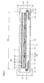
- Fig. 1 shows a schematic cross-sectional view of an example of a solar cell module of the present invention.
- an n-type region 104 and a p-type region 105 are formed, respectively, on an exposed surface from a passivation film 103 formed on a back surface of, for example, a p-type or n-type silicon substrate 101.
- the solar cell module of the present invention has a back electrode type solar cell 100 having a configuration in which an electrode for the n type 106 is formed on n-type region 104, and an electrode for the p type 107 is formed on p-type region 105, and an antireflection film 102 is formed on a light receiving surface of silicon substrate 101. It is noted that the light receiving surface of silicon substrate 101 has a texture structure.
- Electrode for the n type 106 and electrode for the p type 107 of back electrode type solar cell 100 are electrically connected to a wiring for the n type 109 and a wiring for the p type 110 placed on a wiring substrate 111, respectively.
- electrode for the n type 106 of one back electrode type solar cell of adjacent back electrode type solar cells By electrically connecting electrode for the n type 106 of one back electrode type solar cell of adjacent back electrode type solar cells to electrode for the p type 107 of the other back electrode type solar cell, the adjacent back electrode type solar cells are serially connected to configure a solar cell string.
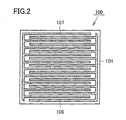
- Fig. 2 shows a schematic plan view of the back surface of back electrode type solar cell 100 shown in Fig. 1 .
- Each of electrode for the n type 106 and electrode for the p type 107 is formed in the shape of a comb on the back surface of silicon substrate 101, and electrode for the n type 106 and electrode for the p type 107 are placed such that teeth of the respective combs are engaged in an alternate manner.
- Each of electrode for the n type 106 and electrode for the p type 107 is preferably made of a metal material, and in particular, of a material including silver.
- Fig. 3 shows a schematic plan view of wiring substrate 111 shown in Fig. 1 .
- wiring for the n type 109 and wiring for the p type 110 are provided, and in addition, a connecting electrode 113 for electrically connecting wiring for the n type 109 that is electrically connected to electrode for the n type 106 of back electrode type solar cell 100 and wiring for the p type 110 that is electrically connected to electrode for the p type 107 is provided.
- a bus bar p electrode 114 for collecting power is electrically connected to wiring for the p type 110 placed at one end in the longitudinal direction of wiring substrate 111, and a bus bar n electrode 115 for collecting power is electrically connected to wiring for the n type 109 placed at the other end.
- a slit 112 serving as an opening for positioning is formed in each of bus bar p electrode 114 and bus bar n electrode 115.
- wiring substrate 111 a flexible film of at least one type selected from the group consisting of PET (polyethylene terephthalate), PEN (polyethylene naphthalate), polyimide, and ethylene vinyl acetate.
- PET polyethylene terephthalate
- PEN polyethylene naphthalate
- polyimide polyimide
- ethylene vinyl acetate a flexible film of at least one type selected from the group consisting of PET (polyethylene terephthalate), PEN (polyethylene naphthalate), polyimide, and ethylene vinyl acetate.
- wiring for the n type 109 wiring for the p type 110, connecting electrode 113, bus bar p electrode 114, and bus bar n electrode 115, a metal material including at least one type selected from the group consisting of silver, copper and aluminum.
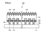
- Fig. 4 shows a schematic cross-sectional view of the solar cell string configured by electrically connecting back electrode type solar cell 100 having the back surface shown in Fig. 2 to wiring substrate 111 shown in Fig. 3 .
- Electrode for the n type 106 of back electrode type solar cell 100 is electrically connected to wiring for the n type 109 on wiring substrate 111 with a conductive material 108 interposed therebetween, and electrode for the p type 107 of back electrode type solar cell 100 is electrically connected to wiring for the p type 110 on wiring substrate 111 with conductive material 108 interposed therebetween.
- solder, a conductive adhesive and the like can be used as the conductive material.
- Fig. 5 shows a schematic plan view of an example of a solar cell structure used in the present invention.
- the solar cell structure is configured by electrically connecting, with a conductive member 116, bus bar p electrode 114 of one solar cell string to bus bar n electrode 115 of the other solar cell string of adjacent solar cell strings that are configured by electrically connecting back electrode type solar cell 100 having the back surface shown in Fig. 2 to wiring substrate 111 shown in Fig. 3 .
- the solar cell strings formed by electrically connecting the plurality of back electrode type solar cells 100 on wiring substrate 111 are electrically connected to each other. Therefore, there are advantages that handling of the individual solar cell strings is easy, that a small reflow furnace is enough for the connection between back electrode type solar cells 100 and wiring substrate 111 by using the solder, the conductive adhesive and the like, as well as that temperature control and workability are easy.
- F Feill Factor
- Fig. 6 shows a schematic plan view of another example of a solar cell structure used in the present invention.
- the solar cell structure is configured by placing a plurality of back electrode type solar cells 100 having the back surfaces shown in Fig. 2 on one wiring substrate 111 on which the wiring for the p type and the wiring for the n type are formed, and electrically connecting the plurality of back electrode type solar cells 100.
- conductive member 116 may be electrically connected to a bus bar electrode portion 122 serving as a portion where the connection direction of back electrode type solar cells 100 is reversed as shown in Fig. 6 , in order to reduce the electrical resistance of the solar cell structure.
- conductive member 116 shown in Figs. 5 and 6 is not particularly limited as long as a member made of a material having conductivity is used.
- a conventionally known interconnector and the like that have been used in the field of solar cells can be used.
- the solar cell structure is sealed in a state where portions of wiring substrate 111 where bus bar p electrode 114 and bus bar n electrode 115 are formed, at opposing ends in the connection direction of back electrode type solar cells 100 of the solar cell structure configured as described above are folded to the side opposite to the light receiving surface side of back electrode type solar cell 100, and as a result, the solar cell module shown in Fig. 1 is obtained.
- each of the opposing ends in the connection direction of back electrode type solar cells 100 of the solar cell structure is folded by using an insulating bar 121 as an axis, and the solar cell structure is sealed into a transparent resin 118 such as EVA between a transparent substrate 117 made of, for example, glass and the like and a base material 119 formed of a weather-resistant film and the like.
- a frame body 120 such as aluminum is put on to surround the periphery of transparent substrate 117, transparent resin 118 and base material 119 that seal the solar cell structure, and as a result, the solar cell module shown in Fig. 1 is obtained.
- the solar cell structure is sealed in a state where the ends of wiring substrate 111 where bus bar portions such as bus bar p electrode 114 and bus bar n electrode 115 are formed are folded to the side opposite to the light receiving surface side of back electrode type solar cell 100. Therefore, flexibility in designing the bus bar portions and conductive member 116 is increased, and the width and the cross-sectional area of the bus bar portions and conductive member 116 can be increased in order to reduce the series resistance between the solar cell strings. Thus, a decrease in the F. F at the time of fabrication of the solar cell module can be suppressed, and a solar cell module having a high F. F can be fabricated.
- the solar cell structure configured as shown in Fig. 5 or 6 is fabricated by using the above method, and insulating bar 121 is placed under slit 112 formed at each of the opposing ends of the solar cell structure.
- a bar having a diameter of about 1 to 2 mm and made of an insulating material such as acrylic can be used as insulating bar 121.
- bar 121 in order to suppress the occurrence of a crack in back electrode type solar cell 100, it is preferable to place bar 121 outside of back electrode type solar cell 100 that is arranged at the end in the connection direction of back electrode type solar cells 100, as shown in Fig. 7(a) , for example.
- the portion of wiring substrate 111 at each of the opposing ends of the solar cell structure is folded to the side opposite to the light receiving surface side of back electrode type solar cell 100 by using bar 121 as the axis.
- a portion having a width of, for example, about 5 to 10 mm from a perimeter of transparent substrate 117 is covered with frame body 120 and forms a shadow that does not contribute to power generation (a portion of the light receiving surface of the solar cell module except for the shadow formed by frame body 120 serves as a light receiving portion of the solar cell module).
- the solar cell structure such that the perimeter portion (e.g., bar 121 and a part of the bus bar portion) except for back electrode type solar cell 100 of the solar cell structure after wiring substrate 111 is folded is located within the shadow formed by frame body 120, that is, such that the portion except for back electrode type solar cell 100 is not exposed at the light receiving portion of the solar cell module as much as possible.
- the perimeter portion e.g., bar 121 and a part of the bus bar portion
- the configuration has been described here in which bar 121 is placed such that the portion of slit 112 is set as a folding position, and the portion of wiring substrate 111 at each of the opposing ends of the solar cell structure is folded by using bar 121 as the axis.
- the portion of wiring substrate 111 at each of the opposing ends of the solar cell structure may be folded to the side opposite to the light receiving surface side of back electrode type solar cell 100 by using the portion of slit 112 as the folding position and without placing bar 121. If the portion of wiring substrate 111 is folded without using bar 121, a fold of the folded portion may have an acute angle and the wiring may be broken.
- Folding the portion of wiring substrate 111 by using bar 121 as the axis leads to lessening of a load applied to the folded portion. Therefore, it is preferable to fold the portion of wiring substrate 111 by using bar 121 as the axis. It is noted that bar 121 may be removed or left as it is when the solar cell structure is sealed.
- the solar cell structure is sealed into transparent resin 118 between transparent substrate 117 such as glass and base material 119 such as the weather-resistant film in a state where the portions of wiring substrate 111 at the opposing ends of the solar cell structure are folded to the side opposite to the light receiving surface side of back electrode type solar cell 100, and frame body 120 made of aluminum and the like is put onto the periphery.
- transparent resin 118 between transparent substrate 117 such as glass and base material 119 such as the weather-resistant film
- a length L1 before folding of the solar cell structure in the connection direction of back electrode type solar cells 100 of the solar cell structure shown in, for example, Fig. 5 or 6 may be made longer than a length L2 of the light receiving portion of the solar cell module in the connection direction of back electrode type solar cells 100 shown in Fig. 1 , in order to increase the width of the wiring to reduce the resistance of the connection between the solar cell strings, and the like.
- the solar cell structure is sealed in a state where the portions of wiring substrate 111 at the opposing ends of the solar cell structure are folded to the side opposite to the light receiving surface side of back electrode type solar cell 100, and as a result, the solar cell module is fabricated. Therefore, the filling ratio can be enhanced, which is a ratio of the total area of the light receiving surface of back electrode type solar cell 100 to the area of the light receiving portion of the solar cell module. Thus, the power generation efficiency of the solar cell module can be enhanced.
- the resistance of the connection between the solar cell strings can be reduced by increasing the width of the wiring of wiring substrate 111. Therefore, the properties of the solar cell module such as the F. F can also be enhanced.
- the electrical connection is possible by placing wiring substrate 111 on the back surface of back electrode type solar cell 100, and it is not necessary to route the interconnector from the light receiving surface to the back surface as in the conventional connection of the solar cells. Therefore, a load applied to back electrode type solar cell 100 at the time of fabrication of the solar cell module is reduced, and the occurrence of a crack in back electrode type solar cell 100 is reduced. Accordingly, according to the present invention, a load applied to back electrode type solar cell 100 at the time of fabrication of the solar cell module can be reduced, and therefore, thinning of back electrode type solar cell 100 can be dealt with.
- a surface of the back electrode type solar cell and the solar cell module on which solar light falls is defined as a light receiving surface, and a surface opposite to the light receiving surface is defined as a back surface.
- the solar cell it is preferable to use, as the solar cell, the back electrode type solar cell in which both of the electrode for the p type and the electrode for the n type are formed on the back surface of the semiconductor substrate such as the silicon substrate, as described above.
- both of the opposing ends in the connection direction of back electrode type solar cells 100 of the solar cell structure are folded.
- any one of the opposing ends in the connection direction of back electrode type solar cells 100 of the solar cell structure may be folded. It is preferable, however, to fold both of the opposing ends in the connection direction of back electrode type solar cells 100 of the solar cell structure, in order to enhance the filling ratio of back electrode type solar cell 100 in the solar cell module.
- a semiconductor substrate except for the silicon substrate may be used, and the p and n conductivity types may be interchanged.
- back electrode type solar cell 100 having the back surface configured as shown in Fig. 2 is prepared.
- the back surface of back electrode type solar cell 100 is a square having a length of one side of 100 mm, and comb-shaped electrode for the n type 106 and electrode for the p type 107 are formed such that the respective electrodes in the shape of the teeth of the combs face each other and are alternately arranged one by one.
- a copper foil having a thickness of 18 ⁇ m is formed on the entire surface of wiring substrate 111 formed of a film of PEN, and then, a part of the copper foil is removed by etching to have a shape shown in Fig. 3 , and wiring for the n type 109, wiring for the p type 110, connecting electrode 113, bus bar p electrode 114, and bus bar n electrode 115 formed of the copper foil left on wiring substrate 111 are formed.
- the wiring is formed to be capable of electrically connecting four back electrode type solar cells 100 in series.
- Connecting electrode 113 is designed such that the distance between adjacent back electrode type solar cells 100 is set to 1 mm.
- the copper foil outside of slit 112 is designed to be set to 50 mm.
- electrode for the n type 106 of back electrode type solar cell 100 is electrically connected to wiring for the n type 109 on wiring substrate 111 with conductive material 108 made of solder interposed therebetween, and in addition, electrode for the p type 107 is electrically connected to wiring for the p type 110 on wiring substrate 111 with conductive material 108 made of solder interposed therebetween, to form the solar cell string in which back electrode type solar cells 100 are serially connected.
- conductive member 116 four solar cell strings fabricated as described above are prepared and serially connected by using the interconnector as conductive member 116 to fabricate the solar cell structure.
- the interconnector As shown in Fig. 5 , four solar cell strings fabricated as described above are prepared and serially connected by using the interconnector as conductive member 116 to fabricate the solar cell structure.
- a thin and wide member that is obtained by coating, with solder, the copper foil having a thickness of 0.08 mm and a width of 30 mm to sufficiently increase the cross-sectional area is used as conductive member 116 implemented as the interconnector.
- EVA ethylene vinyl acetate
- the portion of wiring substrate 111 of the solar cell structure outside of slit 112 is folded to the side opposite to the light receiving surface side of back electrode type solar cell 100 by using bar 121 as the axis, and the EVA sheet and base material 119 formed of the weather-resistant film are placed thereon.
- the EVA sheet stacked by vacuum heating is further heated to crosslink the EVA, and as a result, the solar cell structure is sealed into transparent resin 118 made of the EVA.
- the periphery of the stack of base material 119, transparent resin 118 and transparent substrate 117 is clamped by frame body 120 to fabricate the solar cell module configured as shown in Fig. 1 .
- a shadow portion having a width of 10 mm from the perimeter of transparent substrate 117 is formed in the solar cell module.
- a portion that is located outside of back electrode type solar cell 100 when wiring substrate 111 is folded back has a width of 5 mm.
- clamping by frame body 120 is performed such that the distance between frame body 120 and back electrode type solar cell 100 that is closest to frame body 120 is set to 2 mm.
- the solar cell module fabricated as described above has a very high filling ratio of back electrode type solar cell 100 with respect to the light receiving portion of the solar cell module. Therefore, the high power generation efficiency of the solar cell module is obtained. In addition, since the series resistance due to the wiring between the solar cell strings can be lowered, the excellent F. F of the solar cell module can be obtained.
- the fabrication of the solar cell module fabricated as described above is easy, and thinning of back electrode type solar cell 100 can be dealt with.
- a solar cell module that can deal with thinning of a solar cell, whose power generation efficiency and properties can be enhanced, and furthermore, that can be easily fabricated.
Landscapes
- Photovoltaic Devices (AREA)
Abstract
Description
- The present invention relates to a solar cell module, and in particular, to a solar cell module that can deal with thinning of a solar cell, whose power generation efficiency and properties can be enhanced, and furthermore, that can be easily fabricated at low cost.
- In recent years, it has been desired to develop clean energy because of global environmental problems and the like such as exhaustion of energy resources and an increase in CO2 in the atmosphere. In particular, the photovoltaic power generation using solar cells has been developed, put to practical use and is progressing as a new energy source.
- Conventionally, a solar cell has been a mainstream that is manufactured by diffusing impurities, whose conductivity type is opposite to that of a monocrystalline or polycrystalline silicon substrate, over a surface (light receiving surface) of the silicon substrate on the side on which solar light falls and forming a pn junction near the light receiving surface, and in addition, by arranging one electrode on the light receiving surface and the other electrode on a surface (back surface) located on the side opposite to the light receiving surface.
- A plurality of solar cells configured as described above are electrically connected by an interconnector to form a solar cell string, and the solar cell string is sealed with a resin to fabricate a solar cell module for the photovoltaic power generation.
-
Fig. 8 shows a schematic cross-sectional view of an example of a conventional solar cell module. The conventional solar cell module has a configuration in which a solar cell is fabricated by forming a light receiving surface side electrode (not shown), together with anantireflection film 802, on a light receiving surface on which a texture structure of asilicon substrate 801 is formed and forming a backsurface side electrode 807 on a back surface, and the solar cells are connected by aninterconnector 822 to form a solar cell string, and the solar cell string is sealed into atransparent resin 818. In addition, aglass substrate 817 is placed on an upper surface oftransparent resin 818 that seals the solar cell string, and a weather-resistant film 819 is placed on a lower surface, and the periphery thereof is surrounded by analuminum frame 820. Moreover, a connectingmember 816 for electrically connecting the solar cell string to another solar cell string is provided atinterconnector 822 at each of opposing ends of the solar cell string. - Although the photovoltaic power generation system now becomes widespread gradually, the power generation cost is higher than that of the thermal power generation and the like, and therefore, it is strongly requested to reduce the power generation cost in order to further encourage the widespread use.
- First of all, a method for reducing the power generation cost includes a method for reducing the material cost. Secondly, the method includes a method for enhancing the power generation efficiency of the solar cell module. In other words, if the power generation efficiency can be enhanced at the same material cost, the power generation cost can be relatively reduced.
- If the silicon substrate is thinned in order to reduce the material cost, however, the solar cell is thinned as the silicon substrate is thinned, and a crack may occur in the solar cell during the operation of wiring the solar cell with the interconnector when the solar cell module is fabricated.
- In addition, as shown in
Fig. 8 , when the light receiving surface side electrode (not shown) of the solar cell is connected to backsurface side electrode 807 of another solar cell byinterconnector 822, a space is required to passinterconnector 822 between the solar cells, and furthermore, the space requires a certain degree of size in order to lighten a load applied to an end of the solar cell. Therefore, the filling ratio of the solar cell within the solar cell module is lowered, which is, in turn, responsible for a decrease in the power generation efficiency of the solar cell module. - In addition, in recent years, the development of a so-called back electrode type solar cell having both an electrode for a first conductivity type and an electrode for a second conductivity type (i.e., an electrode for the p type and an electrode for the n type) on a back surface of a silicon substrate has been advancing. Through the use of this back electrode type solar cell, the cells can be connected to each other only on the back surface side of the cells.
- Even in the back electrode type solar cell, however, there are problems related to the occurrence of a crack in the back electrode type solar cell due to thinning of the silicon substrate, and the enhancement of the power generation efficiency of the solar cell module.
- Thus, in Japanese Patent Laying-Open No.
2005-340362 2007-19334 - Patent Document 1: Japanese Patent Laying-Open No.
2005-340362 - Patent Document 2: Japanese Patent Laying-Open No.
2007-19334 - In the method in Patent Document 1, however, it is not attained to enhance the power generation efficiency of the solar cell module by enhancing the filling ratio of the back electrode type solar cell within the solar cell module.
- In addition, in the method in Patent Document 2, it is required to fabricate a solar cell module by performing complicated steps of connecting the wiring substrate to one back electrode type solar cell, and then, further connecting each back electrode type solar cell having the wiring substrate connected thereto to each other. Moreover, although it is proposed to increase the filling ratio of the back electrode type solar cell within the solar cell module by using a printed substrate provided with a throughhole to connect the back electrode type solar cells, an idea of increasing the filling ratio of the back electrode type solar cell without decreasing the F. F of the solar cell module is not attained. Furthermore, a double-sided printed substrate provided with the throughhole is very expensive from the viewpoint of using it in the solar cell module, and is not suitable for use in a commercially available solar cell module.
- In view of the above circumstances, an object of the present invention is to provide a solar cell module that can deal with thinning of a solar cell, whose power generation efficiency and properties can be enhanced, and furthermore, that can be easily fabricated at low cost.
- The present invention is directed to a solar cell module, comprising a solar cell structure formed by electrically connecting a plurality of solar cell strings including a substrate on which a wiring for electrically connecting solar cells to each other is placed and a plurality of solar cells placed on the wiring of the substrate and electrically connected, the solar cell structure being placed with a portion of the substrate at at least one of opposing ends of the solar cell structure folded to a side opposite to a light receiving surface side of the solar cells, each of the solar cell strings having a bus bar portion that is a part of the wiring, on the folded portion of the substrate, and the plurality of solar cell strings being electrically connected by electrically connecting the bus bar portion to another bus bar portion.
- In the solar cell module of the present invention, at least the part of the wiring preferably includes at least one type selected from the group consisting of copper, aluminum and silver.
- In addition, in the solar cell module of the present invention, the bus bar portion that is the part of the wiring preferably includes at least one type selected from the group consisting of silver, copper and aluminum.
- The present invention is directed to a solar cell module, comprising a solar cell structure including a substrate on which a wiring for electrically connecting solar cells to each other is placed and a plurality of solar cells placed on the wiring of the substrate and electrically connected, the solar cell structure being placed with a portion of the substrate at at least one of opposing ends of the solar cell structure folded to a side opposite to a light receiving surface side of the solar cells.
- In addition, in the solar cell module of the present invention, a length before the folding of the solar cell structure in a connection direction of the solar cells is preferably longer than a length of a light receiving portion of the solar cell module in the connection direction of the solar cells.
- In addition, in the solar cell module of the present invention, the substrate is preferably formed of a flexible substrate including at least one type selected from the group consisting of polyethylene terephthalate, polyethylene naphthalate, polyimide, and ethylene vinyl acetate.
- In addition, in the solar cell module of the present invention, the substrate is preferably folded by using a bar made of an insulating material as an axis.
- In addition, in the solar cell module of the present invention, the wiring preferably has an opening for determining at least one of a position for placement of the bar and a position for the folding of the substrate.
- Furthermore, in the solar cell module of the present invention, each of the solar cells is preferably a back electrode type solar cell comprising an electrode for a p type and an electrode for an n type on a back surface opposite to the light receiving surface side of the solar cells.
- According to the present invention, there can be provided a solar cell module that can deal with thinning of a solar cell, whose power generation efficiency and properties can be enhanced, and furthermore, that can be easily fabricated at low cost.
-
-
Fig. 1 is a schematic cross-sectional view of an example of a solar cell module of the present invention. -
Fig. 2 is a schematic plan view of a back surface of a back electrode type solar cell shown inFig. 1 . -
Fig. 3 is a schematic plan view of a wiring substrate shown inFig. 1 . -
Fig. 4 is a schematic cross-sectional view of a solar cell string configured by electrically connecting the back electrode type solar cell having the back surface shown inFig. 2 to the wiring substrate shown inFig. 3 . -
Fig. 5 is a schematic plan view of an example of a solar cell structure used in the present invention. -
Fig. 6 is a schematic plan view of another example of the solar cell structure used in the present invention. -
Fig. 7 is a schematic cross-sectional view for illustrating an example of a method for manufacturing the solar cell module shown inFig. 1 . -
Fig. 8 is a schematic cross-sectional view of an example of a conventional solar cell module. - 100 back electrode type solar cell; 101, 801 silicon substrate; 102, 802 antireflection film; 103 passivation film; 104 n-type region; 105 p-type region; 106 electrode for the n type; 107 electrode for the p type; 108 conductive material; 109 wiring for the n type; 110 wiring for the p type; 111 wiring substrate; 112 slit; 113 connecting electrode; 114 bus bar p electrode; 115 bus bar n electrode; 116 conductive member; 117 transparent substrate; 118, 818 transparent resin; 119 base material; 120 frame body; 121 bar; 122 bus bar electrode portion; 807 back surface side electrode; 816 connecting member; 817 glass substrate; 819 weather-resistant film; 820 aluminum frame; 822 interconnector
- Embodiments of the present invention will be described hereinafter. In the drawings of the present invention, the same reference characters designate the same or corresponding portions.
-
Fig. 1 shows a schematic cross-sectional view of an example of a solar cell module of the present invention. In the solar cell module of the present invention, an n-type region 104 and a p-type region 105 are formed, respectively, on an exposed surface from apassivation film 103 formed on a back surface of, for example, a p-type or n-type silicon substrate 101. The solar cell module of the present invention has a back electrode typesolar cell 100 having a configuration in which an electrode for then type 106 is formed on n-type region 104, and an electrode for thep type 107 is formed on p-type region 105, and anantireflection film 102 is formed on a light receiving surface ofsilicon substrate 101. It is noted that the light receiving surface ofsilicon substrate 101 has a texture structure. - Electrode for the
n type 106 and electrode for thep type 107 of back electrode typesolar cell 100 are electrically connected to a wiring for then type 109 and a wiring for thep type 110 placed on awiring substrate 111, respectively. By electrically connecting electrode for then type 106 of one back electrode type solar cell of adjacent back electrode type solar cells to electrode for thep type 107 of the other back electrode type solar cell, the adjacent back electrode type solar cells are serially connected to configure a solar cell string. -
Fig. 2 shows a schematic plan view of the back surface of back electrode typesolar cell 100 shown inFig. 1 . Each of electrode for then type 106 and electrode for thep type 107 is formed in the shape of a comb on the back surface ofsilicon substrate 101, and electrode for then type 106 and electrode for thep type 107 are placed such that teeth of the respective combs are engaged in an alternate manner. Each of electrode for then type 106 and electrode for thep type 107 is preferably made of a metal material, and in particular, of a material including silver. -
Fig. 3 shows a schematic plan view ofwiring substrate 111 shown inFig. 1 . On the surface ofwiring substrate 111, wiring for then type 109 and wiring for thep type 110 are provided, and in addition, a connectingelectrode 113 for electrically connecting wiring for then type 109 that is electrically connected to electrode for then type 106 of back electrode typesolar cell 100 and wiring for thep type 110 that is electrically connected to electrode for thep type 107 is provided. - In addition, a bus
bar p electrode 114 for collecting power is electrically connected to wiring for thep type 110 placed at one end in the longitudinal direction ofwiring substrate 111, and a busbar n electrode 115 for collecting power is electrically connected to wiring for then type 109 placed at the other end. - Furthermore, a
slit 112 serving as an opening for positioning is formed in each of busbar p electrode 114 and busbar n electrode 115. - It is preferable to use, as
wiring substrate 111, a flexible film of at least one type selected from the group consisting of PET (polyethylene terephthalate), PEN (polyethylene naphthalate), polyimide, and ethylene vinyl acetate. - In addition, it is preferable to use, as wiring for the
n type 109, wiring for thep type 110, connectingelectrode 113, busbar p electrode 114, and busbar n electrode 115, a metal material including at least one type selected from the group consisting of silver, copper and aluminum. - It is noted that, although the respective regions of wiring for the
n type 109, wiring for thep type 110, connectingelectrode 113, busbar p electrode 114, and busbar n electrode 115 are separated by a dashed line inFig. 3 , the present invention is not limited to the separation shown inFig. 3 . -
Fig. 4 shows a schematic cross-sectional view of the solar cell string configured by electrically connecting back electrode typesolar cell 100 having the back surface shown inFig. 2 towiring substrate 111 shown inFig. 3 . Electrode for then type 106 of back electrode typesolar cell 100 is electrically connected to wiring for then type 109 onwiring substrate 111 with aconductive material 108 interposed therebetween, and electrode for thep type 107 of back electrode typesolar cell 100 is electrically connected to wiring for thep type 110 onwiring substrate 111 withconductive material 108 interposed therebetween. For example, solder, a conductive adhesive and the like can be used as the conductive material. -
Fig. 5 shows a schematic plan view of an example of a solar cell structure used in the present invention. The solar cell structure is configured by electrically connecting, with aconductive member 116, busbar p electrode 114 of one solar cell string to busbar n electrode 115 of the other solar cell string of adjacent solar cell strings that are configured by electrically connecting back electrode typesolar cell 100 having the back surface shown inFig. 2 towiring substrate 111 shown inFig. 3 . - In the solar cell structure configured as shown in
Fig. 5 , the solar cell strings formed by electrically connecting the plurality of back electrode typesolar cells 100 onwiring substrate 111 are electrically connected to each other. Therefore, there are advantages that handling of the individual solar cell strings is easy, that a small reflow furnace is enough for the connection between back electrode typesolar cells 100 andwiring substrate 111 by using the solder, the conductive adhesive and the like, as well as that temperature control and workability are easy. - In order to avoid a decrease in the F. F (Fill Factor) of the solar cell module, it is preferable to increase the cross-sectional area of the wiring material, and in particular, it is important to increase the cross-sectional areas of bus
bar p electrode 114 of a solar cell string and busbar n electrode 115 of the other solar cell string as well asconductive member 116, in the solar cell structure shown inFig. 5 (the same is applied as well toFig. 6 ). -
Fig. 6 shows a schematic plan view of another example of a solar cell structure used in the present invention. The solar cell structure is configured by placing a plurality of back electrode typesolar cells 100 having the back surfaces shown inFig. 2 on onewiring substrate 111 on which the wiring for the p type and the wiring for the n type are formed, and electrically connecting the plurality of back electrode typesolar cells 100. - In the solar cell structure configured as shown in
Fig. 6 , only onewiring substrate 111 is used. Therefore, there is an advantage that it is not necessary to electrically connectwiring substrates 111 to each other. - In addition, in the solar cell structure shown in
Fig. 6 ,conductive member 116 may be electrically connected to a busbar electrode portion 122 serving as a portion where the connection direction of back electrode typesolar cells 100 is reversed as shown inFig. 6 , in order to reduce the electrical resistance of the solar cell structure. - It is noted that
conductive member 116 shown inFigs. 5 and6 is not particularly limited as long as a member made of a material having conductivity is used. For example, a conventionally known interconnector and the like that have been used in the field of solar cells can be used. - The solar cell structure is sealed in a state where portions of
wiring substrate 111 where busbar p electrode 114 and busbar n electrode 115 are formed, at opposing ends in the connection direction of back electrode typesolar cells 100 of the solar cell structure configured as described above are folded to the side opposite to the light receiving surface side of back electrode typesolar cell 100, and as a result, the solar cell module shown inFig. 1 is obtained. - At this time, each of the opposing ends in the connection direction of back electrode type
solar cells 100 of the solar cell structure is folded by using an insulatingbar 121 as an axis, and the solar cell structure is sealed into atransparent resin 118 such as EVA between atransparent substrate 117 made of, for example, glass and the like and abase material 119 formed of a weather-resistant film and the like. Then, aframe body 120 such as aluminum is put on to surround the periphery oftransparent substrate 117,transparent resin 118 andbase material 119 that seal the solar cell structure, and as a result, the solar cell module shown inFig. 1 is obtained. - As described above, the solar cell structure is sealed in a state where the ends of
wiring substrate 111 where bus bar portions such as busbar p electrode 114 and busbar n electrode 115 are formed are folded to the side opposite to the light receiving surface side of back electrode typesolar cell 100. Therefore, flexibility in designing the bus bar portions andconductive member 116 is increased, and the width and the cross-sectional area of the bus bar portions andconductive member 116 can be increased in order to reduce the series resistance between the solar cell strings. Thus, a decrease in the F. F at the time of fabrication of the solar cell module can be suppressed, and a solar cell module having a high F. F can be fabricated. - An example of a method for manufacturing the solar cell module shown in
Fig. 1 will be described hereinafter with reference to the schematic cross-sectional views inFigs. 7(a) to (c) . - First, as shown in
Fig. 7(a) , the solar cell structure configured as shown inFig. 5 or6 is fabricated by using the above method, and insulatingbar 121 is placed underslit 112 formed at each of the opposing ends of the solar cell structure. A bar having a diameter of about 1 to 2 mm and made of an insulating material such as acrylic can be used as insulatingbar 121. In addition, in order to suppress the occurrence of a crack in back electrode typesolar cell 100, it is preferable to placebar 121 outside of back electrode typesolar cell 100 that is arranged at the end in the connection direction of back electrode typesolar cells 100, as shown inFig. 7(a) , for example. Moreover, it is preferable to form slit 112 having such a size that does not affect the resistance of the wiring onwiring substrate 111. - Next, as shown in
Fig. 7(b) , the portion ofwiring substrate 111 at each of the opposing ends of the solar cell structure is folded to the side opposite to the light receiving surface side of back electrode typesolar cell 100 by usingbar 121 as the axis. - Generally, when the solar cell structure is sealed into
transparent resin 118 and the like and the periphery thereof is clamped byframe body 120, a portion having a width of, for example, about 5 to 10 mm from a perimeter oftransparent substrate 117 is covered withframe body 120 and forms a shadow that does not contribute to power generation (a portion of the light receiving surface of the solar cell module except for the shadow formed byframe body 120 serves as a light receiving portion of the solar cell module). - Accordingly, in order to eliminate waste of the filling ratio of back electrode type
solar cell 100 within the light receiving surface of the solar cell module, it is preferable to place the solar cell structure such that the perimeter portion (e.g.,bar 121 and a part of the bus bar portion) except for back electrode typesolar cell 100 of the solar cell structure after wiringsubstrate 111 is folded is located within the shadow formed byframe body 120, that is, such that the portion except for back electrode typesolar cell 100 is not exposed at the light receiving portion of the solar cell module as much as possible. - The configuration has been described here in which bar 121 is placed such that the portion of
slit 112 is set as a folding position, and the portion ofwiring substrate 111 at each of the opposing ends of the solar cell structure is folded by usingbar 121 as the axis. In the present invention, however, the portion ofwiring substrate 111 at each of the opposing ends of the solar cell structure may be folded to the side opposite to the light receiving surface side of back electrode typesolar cell 100 by using the portion ofslit 112 as the folding position and without placingbar 121. If the portion ofwiring substrate 111 is folded without usingbar 121, a fold of the folded portion may have an acute angle and the wiring may be broken. Folding the portion ofwiring substrate 111 by usingbar 121 as the axis leads to lessening of a load applied to the folded portion. Therefore, it is preferable to fold the portion ofwiring substrate 111 by usingbar 121 as the axis. It is noted thatbar 121 may be removed or left as it is when the solar cell structure is sealed. - Thereafter, as shown in
Fig. 7(c) , the solar cell structure is sealed intotransparent resin 118 betweentransparent substrate 117 such as glass andbase material 119 such as the weather-resistant film in a state where the portions ofwiring substrate 111 at the opposing ends of the solar cell structure are folded to the side opposite to the light receiving surface side of back electrode typesolar cell 100, andframe body 120 made of aluminum and the like is put onto the periphery. As a result, the solar cell module configured as shown inFig. 1 is fabricated. - In the solar cell module fabricated as described above, a length L1 before folding of the solar cell structure in the connection direction of back electrode type
solar cells 100 of the solar cell structure shown in, for example,Fig. 5 or6 (inFigs. 5 and6 , for example, the vertical direction of the papers ofFigs. 5 and6 ) may be made longer than a length L2 of the light receiving portion of the solar cell module in the connection direction of back electrode typesolar cells 100 shown inFig. 1 , in order to increase the width of the wiring to reduce the resistance of the connection between the solar cell strings, and the like. - Even in such a case, in the present invention, the solar cell structure is sealed in a state where the portions of
wiring substrate 111 at the opposing ends of the solar cell structure are folded to the side opposite to the light receiving surface side of back electrode typesolar cell 100, and as a result, the solar cell module is fabricated. Therefore, the filling ratio can be enhanced, which is a ratio of the total area of the light receiving surface of back electrode typesolar cell 100 to the area of the light receiving portion of the solar cell module. Thus, the power generation efficiency of the solar cell module can be enhanced. In addition, in the present invention, the resistance of the connection between the solar cell strings can be reduced by increasing the width of the wiring ofwiring substrate 111. Therefore, the properties of the solar cell module such as the F. F can also be enhanced. - In addition, in the present invention, the electrical connection is possible by placing
wiring substrate 111 on the back surface of back electrode typesolar cell 100, and it is not necessary to route the interconnector from the light receiving surface to the back surface as in the conventional connection of the solar cells. Therefore, a load applied to back electrode typesolar cell 100 at the time of fabrication of the solar cell module is reduced, and the occurrence of a crack in back electrode typesolar cell 100 is reduced. Accordingly, according to the present invention, a load applied to back electrode typesolar cell 100 at the time of fabrication of the solar cell module can be reduced, and therefore, thinning of back electrode typesolar cell 100 can be dealt with. - Furthermore, in the present invention, it is not necessary to provide one
wiring substrate 111 for each back electrode typesolar cell 100. Therefore, the fabrication of the solar cell module can be facilitated. - It is noted that, in the specification, a surface of the back electrode type solar cell and the solar cell module on which solar light falls is defined as a light receiving surface, and a surface opposite to the light receiving surface is defined as a back surface.
- In addition, in the present invention, it is preferable to use, as the solar cell, the back electrode type solar cell in which both of the electrode for the p type and the electrode for the n type are formed on the back surface of the semiconductor substrate such as the silicon substrate, as described above.
- In addition, in the above, it has been described that both of the opposing ends in the connection direction of back electrode type
solar cells 100 of the solar cell structure are folded. In the present invention, however, any one of the opposing ends in the connection direction of back electrode typesolar cells 100 of the solar cell structure may be folded. It is preferable, however, to fold both of the opposing ends in the connection direction of back electrode typesolar cells 100 of the solar cell structure, in order to enhance the filling ratio of back electrode typesolar cell 100 in the solar cell module. - In addition, in the present invention, a semiconductor substrate except for the silicon substrate may be used, and the p and n conductivity types may be interchanged.
- First, back electrode type
solar cell 100 having the back surface configured as shown inFig. 2 is prepared. The back surface of back electrode typesolar cell 100 is a square having a length of one side of 100 mm, and comb-shaped electrode for then type 106 and electrode for thep type 107 are formed such that the respective electrodes in the shape of the teeth of the combs face each other and are alternately arranged one by one. - A copper foil having a thickness of 18 µm is formed on the entire surface of
wiring substrate 111 formed of a film of PEN, and then, a part of the copper foil is removed by etching to have a shape shown inFig. 3 , and wiring for then type 109, wiring for thep type 110, connectingelectrode 113, busbar p electrode 114, and busbar n electrode 115 formed of the copper foil left onwiring substrate 111 are formed. Thus, the wiring is formed to be capable of electrically connecting four back electrode typesolar cells 100 in series. - Connecting
electrode 113 is designed such that the distance between adjacent back electrode typesolar cells 100 is set to 1 mm. In addition, the copper foil outside ofslit 112 is designed to be set to 50 mm. - Next, as shown in
Fig. 4 , by using the reflow furnace, electrode for then type 106 of back electrode typesolar cell 100 is electrically connected to wiring for then type 109 onwiring substrate 111 withconductive material 108 made of solder interposed therebetween, and in addition, electrode for thep type 107 is electrically connected to wiring for thep type 110 onwiring substrate 111 withconductive material 108 made of solder interposed therebetween, to form the solar cell string in which back electrode typesolar cells 100 are serially connected. - Next, as shown in
Fig. 5 , four solar cell strings fabricated as described above are prepared and serially connected by using the interconnector asconductive member 116 to fabricate the solar cell structure. In order to avoid a load applied to back electrode typesolar cell 100 when wiringsubstrate 111 at the opposing ends of the solar cell structure is folded, a thin and wide member that is obtained by coating, with solder, the copper foil having a thickness of 0.08 mm and a width of 30 mm to sufficiently increase the cross-sectional area is used asconductive member 116 implemented as the interconnector. - Thereafter, an EVA (ethylene vinyl acetate) sheet is placed on
transparent substrate 117 made of glass, and the above solar cell structure is placed thereon such that the light receiving surface side of back electrode typesolar cell 100 faces downward. As shown inFig. 7(a) ,bar 121 made of acrylic and having a diameter of 1.5 mm is placed at the position ofslit 112. - Thereafter, as shown in
Fig. 7(b) , the portion ofwiring substrate 111 of the solar cell structure outside ofslit 112 is folded to the side opposite to the light receiving surface side of back electrode typesolar cell 100 by usingbar 121 as the axis, and the EVA sheet andbase material 119 formed of the weather-resistant film are placed thereon. The EVA sheet stacked by vacuum heating is further heated to crosslink the EVA, and as a result, the solar cell structure is sealed intotransparent resin 118 made of the EVA. - Finally, the periphery of the stack of
base material 119,transparent resin 118 andtransparent substrate 117 is clamped byframe body 120 to fabricate the solar cell module configured as shown inFig. 1 . At this time, a shadow portion having a width of 10 mm from the perimeter oftransparent substrate 117 is formed in the solar cell module. In addition, a portion that is located outside of back electrode typesolar cell 100 when wiringsubstrate 111 is folded back has a width of 5 mm. Moreover, clamping byframe body 120 is performed such that the distance betweenframe body 120 and back electrode typesolar cell 100 that is closest to framebody 120 is set to 2 mm. - The solar cell module fabricated as described above has a very high filling ratio of back electrode type
solar cell 100 with respect to the light receiving portion of the solar cell module. Therefore, the high power generation efficiency of the solar cell module is obtained. In addition, since the series resistance due to the wiring between the solar cell strings can be lowered, the excellent F. F of the solar cell module can be obtained. - Furthermore, the fabrication of the solar cell module fabricated as described above is easy, and thinning of back electrode type
solar cell 100 can be dealt with. - It should be understood that the embodiments disclosed herein are illustrative and not limitative in any respect. The scope of the present invention is defined by the terms of the claims, rather than the above description, and is intended to include any modifications within the scope and meaning equivalent to the terms of the claims.
- According to the present invention, there can be provided a solar cell module that can deal with thinning of a solar cell, whose power generation efficiency and properties can be enhanced, and furthermore, that can be easily fabricated.
Claims (14)
- A solar cell module, comprising a solar cell structure formed by electrically connecting a plurality of solar cell strings including a substrate (111) on which a wiring (109, 110) for electrically connecting solar cells (100) to each other is placed and a plurality of solar cells (100) placed on said wiring (109, 110) of said substrate (111) and electrically connected,
said solar cell structure being placed with a portion of said substrate (111) at at least one of opposing ends of said solar cell structure folded to a side opposite to a light receiving surface side of said solar cells (100),
each of said solar cell strings having a bus bar portion (114, 115) that is a part of said wiring (109, 110), on said portion of said substrate (111) folded, and
said plurality of solar cell strings being electrically connected by electrically connecting said bus bar portion (114, 115) to another said bus bar portion (114, 115). - The solar cell module according to claim 1, wherein
at least the part of said wiring (109, 110) includes at least one type selected from the group consisting of copper, aluminum and silver. - The solar cell module according to claim 1, wherein
said bus bar portion (114, 115) includes at least one type selected from the group consisting of silver, copper and aluminum. - The solar cell module according to claim 1, wherein
a length before said folding of said solar cell structure in a connection direction of said solar cells (100) is longer than a length of a light receiving portion of said solar cell module in the connection direction of said solar cells (100). - The solar cell module according to claim 1, wherein
said substrate (111) is a flexible substrate (111) including at least one type selected from the group consisting of polyethylene terephthalate, polyethylene naphthalate, polyimide, and ethylene vinyl acetate. - The solar cell module according to claim 1, wherein
said substrate (111) is folded by using a bar (121) made of an insulating material as an axis. - The solar cell module according to claim 6, wherein
said wiring (109, 110) has an opening (112) for determining at least one of a position for placement of said bar (121) and a position for said folding of said substrate (111). - The solar cell module according to claim 1, wherein
each of said solar cells (100) is a back electrode type solar cell (100) comprising an electrode for a p type (107) and an electrode for an n type (106) on a back surface opposite to the light receiving surface side of said solar cells (100). - A solar cell module, comprising a solar cell structure including a substrate (111) on which a wiring (109, 110) for electrically connecting solar cells (100) to each other is placed and a plurality of solar cells (100) placed on said wiring (109, 110) of said substrate (111) and electrically connected,
said solar cell structure being placed with a portion of said substrate (111) at at least one of opposing ends of said solar cell structure folded to a side opposite to a light receiving surface side of said solar cells (100). - The solar cell module according to claim 9, wherein
a length before said folding of said solar cell structure in a connection direction of said solar cells (100) is longer than a length of a light receiving portion of said solar cell module in the connection direction of said solar cells (100). - The solar cell module according to claim 9, wherein
said substrate (111) is a flexible substrate including at least one type selected from the group consisting of polyethylene terephthalate, polyethylene naphthalate, polyimide, and ethylene vinyl acetate. - The solar cell module according to claim 9, wherein
said substrate (111) is folded by using a bar (121) made of an insulating material as an axis. - The solar cell module according to claim 12, wherein
said wiring (109, 110) has an opening for determining at least one of a position for placement of said bar (121) and a position for said folding of said substrate (111). - The solar cell module according to claim 9, wherein
each of said solar cells (100) is a back electrode type solar cell comprising an electrode for a p type (107) and an electrode for an n type (106) on a back surface opposite to the light receiving surface side of said solar cells (100).
Applications Claiming Priority (2)
| Application Number | Priority Date | Filing Date | Title |
|---|---|---|---|
| JP2007205681A JP2009043842A (en) | 2007-08-07 | 2007-08-07 | Solar cell module |
| PCT/JP2008/061819 WO2009019940A1 (en) | 2007-08-07 | 2008-06-30 | Solar cell module |
Publications (2)
| Publication Number | Publication Date |
|---|---|
| EP2180521A1 true EP2180521A1 (en) | 2010-04-28 |
| EP2180521A4 EP2180521A4 (en) | 2014-09-10 |
Family
ID=40341176
Family Applications (1)
| Application Number | Title | Priority Date | Filing Date |
|---|---|---|---|
| EP08790732.5A Withdrawn EP2180521A4 (en) | 2007-08-07 | 2008-06-30 | SOLAR CELL MODULE |
Country Status (5)
| Country | Link |
|---|---|
| US (1) | US20110155203A1 (en) |
| EP (1) | EP2180521A4 (en) |
| JP (1) | JP2009043842A (en) |
| CN (1) | CN101779297B (en) |
| WO (1) | WO2009019940A1 (en) |
Cited By (3)
| Publication number | Priority date | Publication date | Assignee | Title |
|---|---|---|---|---|
| EP2329530A4 (en) * | 2008-08-27 | 2013-03-20 | Applied Materials Inc | PHOTOPIL MODULES WITH REAR CONTACTS |
| EP2423973A4 (en) * | 2009-04-23 | 2013-08-28 | Sharp Kk | WIRING SHEET, SOLAR CELL COMPRISING THE WIRING SHEET, AND SOLAR CELL MODULE |
| US8993875B2 (en) | 2008-07-02 | 2015-03-31 | Sharp Kabushiki Kaisha | Solar battery module and method for manufacturing the same |
Families Citing this family (37)
| Publication number | Priority date | Publication date | Assignee | Title |
|---|---|---|---|---|
| WO2009116394A1 (en) * | 2008-03-17 | 2009-09-24 | シャープ株式会社 | Solar battery module and method for manufacturing solar battery module |
| CN102362363A (en) * | 2009-03-23 | 2012-02-22 | 夏普株式会社 | Solar cell with wiring board, solar cell module, and method for manufacturing solar cell with wiring board |
| JP5288409B2 (en) * | 2009-04-08 | 2013-09-11 | シャープ株式会社 | Solar cell with wiring sheet, solar cell module, method for manufacturing solar cell with wiring sheet, and method for manufacturing solar cell module |
| JP5154516B2 (en) * | 2009-05-22 | 2013-02-27 | シャープ株式会社 | Solar cell module and method for manufacturing solar cell module |
| JP5242499B2 (en) * | 2009-05-25 | 2013-07-24 | シャープ株式会社 | SOLAR CELL MODULE, ITS MANUFACTURING METHOD, AND ELECTRONIC DEVICE MOUNTED WITH THE SOLAR CELL MODULE |
| WO2010150735A1 (en) * | 2009-06-22 | 2010-12-29 | シャープ株式会社 | Wiring sheet, solar cell with wiring sheet attached, wiring sheet roll, solar cell module, and method for producing wiring sheet |
| JP5273729B2 (en) * | 2009-06-22 | 2013-08-28 | シャープ株式会社 | Wiring sheet, solar cell with wiring sheet, solar cell module, and wiring sheet roll |
| JP2011108969A (en) * | 2009-11-20 | 2011-06-02 | Hitachi Cable Ltd | Method of manufacturing solar cell module and wiring board for solar cell |
| KR101085475B1 (en) * | 2009-12-21 | 2011-11-21 | 삼성전기주식회사 | Solar cell module and its manufacturing method |
| US9450126B1 (en) * | 2010-06-18 | 2016-09-20 | The Boeing Company | Solar cell module |
| JPWO2013046773A1 (en) * | 2011-09-29 | 2015-03-26 | 三洋電機株式会社 | Solar cell module |
| US8328077B1 (en) * | 2011-11-01 | 2012-12-11 | Flextronics Ap, Llc | PV cell mass reflow |
| KR101305624B1 (en) * | 2011-11-01 | 2013-09-09 | 엘지이노텍 주식회사 | Solar cell module and method of fabricating the same |
| WO2014002975A1 (en) | 2012-06-25 | 2014-01-03 | 三洋電機株式会社 | Solar cell module |
| JPWO2014030225A1 (en) | 2012-08-22 | 2016-07-28 | パナソニックIpマネジメント株式会社 | Solar cell module and manufacturing method thereof |
| JP5456128B2 (en) * | 2012-09-27 | 2014-03-26 | シャープ株式会社 | Solar cell module |
| JP6047389B2 (en) * | 2012-12-07 | 2016-12-21 | シャープ株式会社 | Solar cell and method for manufacturing the same |
| US8936709B2 (en) | 2013-03-13 | 2015-01-20 | Gtat Corporation | Adaptable free-standing metallic article for semiconductors |
| US9685568B2 (en) | 2014-03-12 | 2017-06-20 | Merlin Solar Technologies, Inc. | Photovoltaic module with flexible circuit |
| CN104638040A (en) * | 2013-11-13 | 2015-05-20 | 财团法人工业技术研究院 | solar battery pack |
| US9401438B2 (en) | 2013-11-13 | 2016-07-26 | Industrial Technology Research Institute | Solar cell module and solar cell thereof |
| US20160126380A1 (en) * | 2014-10-30 | 2016-05-05 | Sung Un CHANG | Flexible solar panel and method of fabricating the same |
| CN106098803B (en) * | 2015-05-22 | 2017-10-17 | 苏州沃特维自动化系统有限公司 | A kind of solar battery sheet unit preparation method and solar cell module |
| JP2017017171A (en) * | 2015-06-30 | 2017-01-19 | 大日本印刷株式会社 | Current collector sheet for solar battery module and solar battery module using the same |
| CN105489684A (en) * | 2016-02-03 | 2016-04-13 | 江苏赛拉弗光伏系统有限公司 | Solar photovoltaic assembly |
| CN106328747B (en) * | 2016-10-31 | 2018-02-06 | 苏州宇邦新型材料股份有限公司 | A kind of bending step welding and its processing technology for photovoltaic module |
| JP6772937B2 (en) * | 2017-04-10 | 2020-10-21 | 株式会社オートネットワーク技術研究所 | Storage pack base plate structure and storage pack |
| CN107681008B (en) * | 2017-09-20 | 2024-01-30 | 苏州宇邦新型材料股份有限公司 | Photovoltaic module is with converging area |
| JP2021500498A (en) * | 2017-10-27 | 2021-01-07 | フィジー グループ ビー.ブイ. | Glazing assemblies with an integrated photovoltaic structure and spacer structures for such glazing assemblies |
| CN109638098B (en) * | 2018-12-03 | 2020-07-24 | 珠海格力电器股份有限公司 | A battery pack structure, photovoltaic module and production method |
| JP7441009B2 (en) * | 2019-04-05 | 2024-02-29 | シャープ株式会社 | solar module |
| TWI888529B (en) * | 2020-04-09 | 2025-07-01 | 日商鐘化股份有限公司 | Solar battery module |
| CN111430470B (en) * | 2020-04-22 | 2025-01-28 | 环晟光伏(江苏)有限公司 | A foldable busbar, circuit connection structure and shingled assembly |
| KR102367612B1 (en) * | 2020-04-29 | 2022-02-24 | 엘지전자 주식회사 | Solar cell panel and method for manufacturing the same |
| CN112234120B (en) * | 2020-09-04 | 2022-07-01 | 英利能源(中国)有限公司 | PV module laying method |
| WO2023092257A1 (en) * | 2021-11-23 | 2023-06-01 | China Triumph International Engineering Co., Ltd. | Method for producing a photovoltaic module with edge protection and a photovoltaic module with edge protection |
| JP2025112367A (en) * | 2024-01-19 | 2025-08-01 | Tdk株式会社 | Solar cell |
Family Cites Families (40)
| Publication number | Priority date | Publication date | Assignee | Title |
|---|---|---|---|---|
| US3686815A (en) * | 1970-02-19 | 1972-08-29 | Robert J Von Bose | Method for building construction |
| JPS5224481A (en) * | 1975-08-19 | 1977-02-23 | Sharp Corp | Solar battery module |
| JPS5394194A (en) * | 1977-01-28 | 1978-08-17 | Toshiba Corp | Substrate for photoelectric transducer |
| US4200472A (en) * | 1978-06-05 | 1980-04-29 | The Regents Of The University Of California | Solar power system and high efficiency photovoltaic cells used therein |
| US4392009A (en) * | 1981-10-16 | 1983-07-05 | Exxon Research And Engineering Co. | Solar power module |
| JPS60123073A (en) * | 1983-12-08 | 1985-07-01 | Fuji Electric Corp Res & Dev Ltd | Thin-film solar cell |
| JPS61134080A (en) * | 1984-12-04 | 1986-06-21 | Matsushita Electric Ind Co Ltd | Thin film solar cell |
| JPS63287077A (en) * | 1987-05-20 | 1988-11-24 | Hitachi Ltd | Photoelectric conversion device |
| JPH0240967A (en) * | 1988-07-30 | 1990-02-09 | Nitto Denko Corp | Optoelectric conversion type batteries and hybrid type secondary battery constituted by combining them |
| JPH0415962A (en) * | 1990-05-09 | 1992-01-21 | Sharp Corp | Solar cell and manufacture thereof |
| US5253300A (en) * | 1991-03-22 | 1993-10-12 | H. C. Knapp Sound Technology Inc. | Solar powered hearing aid |
| JPH06310744A (en) * | 1993-04-26 | 1994-11-04 | Fuji Electric Co Ltd | Thin film solar cell module and connection method thereof |
| TW280962B (en) * | 1995-02-24 | 1996-07-11 | Sanyo Electric Co | Battery charger and a solar battery used for charging a battery |
| JPH0997917A (en) * | 1995-09-29 | 1997-04-08 | Sanyo Electric Co Ltd | Foldable solar cell device |
| US5951786A (en) * | 1997-12-19 | 1999-09-14 | Sandia Corporation | Laminated photovoltaic modules using back-contact solar cells |
| US5972732A (en) * | 1997-12-19 | 1999-10-26 | Sandia Corporation | Method of monolithic module assembly |
| JP2000223729A (en) * | 1999-01-28 | 2000-08-11 | Canon Inc | Photovoltaic roof and photovoltaic power generator |
| JP4017340B2 (en) * | 2000-12-15 | 2007-12-05 | 三洋電機株式会社 | Method for manufacturing photovoltaic device |
| NO319368B1 (en) * | 2003-08-19 | 2005-07-18 | Betek Norge As | Device at junction box |
| CN101504956B (en) * | 2003-11-27 | 2012-01-11 | 京瓷株式会社 | Solar cell module |
| JP4681806B2 (en) * | 2003-12-19 | 2011-05-11 | キヤノン株式会社 | Solar cell module |
| US20070295381A1 (en) * | 2004-03-29 | 2007-12-27 | Kyocera Corporation | Solar Cell Module and Photovoltaic Power Generator Using This |
| US7406800B2 (en) * | 2004-05-18 | 2008-08-05 | Andalay Solar, Inc. | Mounting system for a solar panel |
| JP2005340362A (en) | 2004-05-25 | 2005-12-08 | Sharp Corp | Solar cell and solar cell module |
| DE102004025627A1 (en) * | 2004-05-25 | 2005-12-22 | Tyco Electronics Amp Gmbh | Solar module with connection element |
| US7282728B2 (en) * | 2004-09-03 | 2007-10-16 | Steril-Aire, Inc. | Modular fixture |
| DE102004044061A1 (en) * | 2004-09-11 | 2006-04-20 | Rwe Space Solar Power Gmbh | Solar cell arrangement and method for interconnecting a solar cell string |
| JP2007019334A (en) | 2005-07-08 | 2007-01-25 | Mitsubishi Electric Corp | Solar cell device |
| US7982129B2 (en) * | 2005-08-15 | 2011-07-19 | Konarka Technologies, Inc. | Photovoltaic cells with interconnects to external circuit |
| US20070095384A1 (en) * | 2005-10-28 | 2007-05-03 | Farquhar Donald S | Photovoltaic modules and interconnect methodology for fabricating the same |
| JP4662151B2 (en) * | 2005-11-29 | 2011-03-30 | 大日本印刷株式会社 | Filler for solar cell module, solar cell module using the same, and method for producing filler for solar cell module |
| JP2007294866A (en) * | 2006-03-31 | 2007-11-08 | Sanyo Electric Co Ltd | Solar cell module |
| WO2008088570A1 (en) * | 2006-04-18 | 2008-07-24 | Itn Energy Systems, Inc. | Reinforcing structures for thin-film photovoltaic device substrates, and associated methods |
| US20070283997A1 (en) * | 2006-06-13 | 2007-12-13 | Miasole | Photovoltaic module with integrated current collection and interconnection |
| US20080041434A1 (en) * | 2006-08-18 | 2008-02-21 | Nanosolar, Inc. | Methods and devices for large-scale solar installations |
| US20090032087A1 (en) * | 2007-02-06 | 2009-02-05 | Kalejs Juris P | Manufacturing processes for light concentrating solar module |
| US7622672B2 (en) * | 2007-03-07 | 2009-11-24 | Johnson Richard A | Electrical housing knockout device and method |
| US20090025778A1 (en) * | 2007-07-23 | 2009-01-29 | Day4 Energy Inc. | Shading protection for solar cells and solar cell modules |
| KR20100097219A (en) * | 2007-12-18 | 2010-09-02 | 데이4 에너지 인코포레이티드 | Photovoltaic module with edge access to pv strings, interconnection method, apparatus, and system |
| WO2009116394A1 (en) * | 2008-03-17 | 2009-09-24 | シャープ株式会社 | Solar battery module and method for manufacturing solar battery module |
-
2007
- 2007-08-07 JP JP2007205681A patent/JP2009043842A/en active Pending
-
2008
- 2008-06-30 US US12/672,278 patent/US20110155203A1/en not_active Abandoned
- 2008-06-30 WO PCT/JP2008/061819 patent/WO2009019940A1/en not_active Ceased
- 2008-06-30 CN CN2008801023944A patent/CN101779297B/en active Active
- 2008-06-30 EP EP08790732.5A patent/EP2180521A4/en not_active Withdrawn
Cited By (3)
| Publication number | Priority date | Publication date | Assignee | Title |
|---|---|---|---|---|
| US8993875B2 (en) | 2008-07-02 | 2015-03-31 | Sharp Kabushiki Kaisha | Solar battery module and method for manufacturing the same |
| EP2329530A4 (en) * | 2008-08-27 | 2013-03-20 | Applied Materials Inc | PHOTOPIL MODULES WITH REAR CONTACTS |
| EP2423973A4 (en) * | 2009-04-23 | 2013-08-28 | Sharp Kk | WIRING SHEET, SOLAR CELL COMPRISING THE WIRING SHEET, AND SOLAR CELL MODULE |
Also Published As
| Publication number | Publication date |
|---|---|
| US20110155203A1 (en) | 2011-06-30 |
| JP2009043842A (en) | 2009-02-26 |
| EP2180521A4 (en) | 2014-09-10 |
| CN101779297B (en) | 2013-09-11 |
| WO2009019940A1 (en) | 2009-02-12 |
| CN101779297A (en) | 2010-07-14 |
Similar Documents
| Publication | Publication Date | Title |
|---|---|---|
| EP2180521A1 (en) | Solar cell module | |
| CN102959723B (en) | Solar module and manufacture method thereof | |
| KR102274685B1 (en) | Shingled array solar cells and method of manufacturing solar modules including the same | |
| JP5714080B2 (en) | Solar cell module | |
| EP2423973A1 (en) | Wiring sheet, solar cell provided with wiring sheet, and solar cell module | |
| US8609983B2 (en) | Interconnection sheet, solar cell with interconnection sheet, solar cell module, and interconnection sheet roll | |
| US20160163903A1 (en) | High-efficiency pv panel with conductive backsheet | |
| US20090050190A1 (en) | Solar cell and solar cell module | |
| JP5927437B2 (en) | Solar cell module | |
| JP7002558B2 (en) | How to make bus barless tiled array solar cells and solar cells | |
| US20120318351A1 (en) | Solar cell having a special busbar shape, solar cell arrangement containing said solar cell, and method for producing the solar cell | |
| CN103329285B (en) | The lead connecting method of solar battery cell, solar module and solar battery cell | |
| JP5299975B2 (en) | Back electrode type solar cell, wiring sheet, solar cell with wiring sheet and solar cell module | |
| JP2005183660A (en) | Solar cell module | |
| JP5203176B2 (en) | Wiring sheet, solar cell with wiring sheet and solar cell module | |
| JP2002359388A (en) | Solar cell device | |
| EP2219227B1 (en) | Solar cell | |
| CN102668113B (en) | solar cell module | |
| JP2013093610A (en) | Solar cell structure and solar cell module | |
| CN102687279B (en) | Solar battery cell | |
| WO2013094556A1 (en) | Solar cell with wiring sheet, solar cell module, and solar cell manufacturing method | |
| JP2005167161A (en) | Manufacturing method of solar cell module | |
| JP2006278695A (en) | Solar cell module | |
| JP4036880B2 (en) | Method for manufacturing solar cell and method for manufacturing solar cell module | |
| KR20190043295A (en) | Stile type solar cell module using divided cell |
Legal Events
| Date | Code | Title | Description |
|---|---|---|---|
| PUAI | Public reference made under article 153(3) epc to a published international application that has entered the european phase |
Free format text: ORIGINAL CODE: 0009012 |
|
| 17P | Request for examination filed |
Effective date: 20100211 |
|
| AK | Designated contracting states |
Kind code of ref document: A1 Designated state(s): AT BE BG CH CY CZ DE DK EE ES FI FR GB GR HR HU IE IS IT LI LT LU LV MC MT NL NO PL PT RO SE SI SK TR |
|
| AX | Request for extension of the european patent |
Extension state: AL BA MK RS |
|
| DAX | Request for extension of the european patent (deleted) | ||
| A4 | Supplementary search report drawn up and despatched |
Effective date: 20140812 |
|
| RIC1 | Information provided on ipc code assigned before grant |
Ipc: H01L 31/05 20140101AFI20140806BHEP Ipc: H01L 31/02 20060101ALI20140806BHEP |
|
| STAA | Information on the status of an ep patent application or granted ep patent |
Free format text: STATUS: THE APPLICATION IS DEEMED TO BE WITHDRAWN |
|
| 18D | Application deemed to be withdrawn |
Effective date: 20150310 |