EP2178080B1 - Leistungszuweisungsverfahren und -vorrichtung - Google Patents
Leistungszuweisungsverfahren und -vorrichtung Download PDFInfo
- Publication number
- EP2178080B1 EP2178080B1 EP09251531.1A EP09251531A EP2178080B1 EP 2178080 B1 EP2178080 B1 EP 2178080B1 EP 09251531 A EP09251531 A EP 09251531A EP 2178080 B1 EP2178080 B1 EP 2178080B1
- Authority
- EP
- European Patent Office
- Prior art keywords
- performance
- graphics processor
- workload
- frame
- processor
- Prior art date
- Legal status (The legal status is an assumption and is not a legal conclusion. Google has not performed a legal analysis and makes no representation as to the accuracy of the status listed.)
- Active
Links
Images


Classifications
-
- G—PHYSICS
- G06—COMPUTING OR CALCULATING; COUNTING
- G06T—IMAGE DATA PROCESSING OR GENERATION, IN GENERAL
- G06T1/00—General purpose image data processing
-
- G—PHYSICS
- G06—COMPUTING OR CALCULATING; COUNTING
- G06F—ELECTRIC DIGITAL DATA PROCESSING
- G06F9/00—Arrangements for program control, e.g. control units
- G06F9/06—Arrangements for program control, e.g. control units using stored programs, i.e. using an internal store of processing equipment to receive or retain programs
- G06F9/46—Multiprogramming arrangements
- G06F9/50—Allocation of resources, e.g. of the central processing unit [CPU]
-
- G—PHYSICS
- G06—COMPUTING OR CALCULATING; COUNTING
- G06F—ELECTRIC DIGITAL DATA PROCESSING
- G06F1/00—Details not covered by groups G06F3/00 - G06F13/00 and G06F21/00
- G06F1/26—Power supply means, e.g. regulation thereof
- G06F1/32—Means for saving power
- G06F1/3203—Power management, i.e. event-based initiation of a power-saving mode
-
- G—PHYSICS
- G06—COMPUTING OR CALCULATING; COUNTING
- G06F—ELECTRIC DIGITAL DATA PROCESSING
- G06F1/00—Details not covered by groups G06F3/00 - G06F13/00 and G06F21/00
- G06F1/26—Power supply means, e.g. regulation thereof
- G06F1/32—Means for saving power
-
- G—PHYSICS
- G06—COMPUTING OR CALCULATING; COUNTING
- G06F—ELECTRIC DIGITAL DATA PROCESSING
- G06F1/00—Details not covered by groups G06F3/00 - G06F13/00 and G06F21/00
- G06F1/26—Power supply means, e.g. regulation thereof
- G06F1/32—Means for saving power
- G06F1/3203—Power management, i.e. event-based initiation of a power-saving mode
- G06F1/3234—Power saving characterised by the action undertaken
- G06F1/324—Power saving characterised by the action undertaken by lowering clock frequency
-
- G—PHYSICS
- G06—COMPUTING OR CALCULATING; COUNTING
- G06F—ELECTRIC DIGITAL DATA PROCESSING
- G06F9/00—Arrangements for program control, e.g. control units
-
- G—PHYSICS
- G06—COMPUTING OR CALCULATING; COUNTING
- G06T—IMAGE DATA PROCESSING OR GENERATION, IN GENERAL
- G06T1/00—General purpose image data processing
- G06T1/20—Processor architectures; Processor configuration, e.g. pipelining
-
- G—PHYSICS
- G09—EDUCATION; CRYPTOGRAPHY; DISPLAY; ADVERTISING; SEALS
- G09G—ARRANGEMENTS OR CIRCUITS FOR CONTROL OF INDICATING DEVICES USING STATIC MEANS TO PRESENT VARIABLE INFORMATION
- G09G5/00—Control arrangements or circuits for visual indicators common to cathode-ray tube indicators and other visual indicators
- G09G5/001—Arbitration of resources in a display system, e.g. control of access to frame buffer by video controller and/or main processor
-
- G—PHYSICS
- G09—EDUCATION; CRYPTOGRAPHY; DISPLAY; ADVERTISING; SEALS
- G09G—ARRANGEMENTS OR CIRCUITS FOR CONTROL OF INDICATING DEVICES USING STATIC MEANS TO PRESENT VARIABLE INFORMATION
- G09G5/00—Control arrangements or circuits for visual indicators common to cathode-ray tube indicators and other visual indicators
- G09G5/36—Control arrangements or circuits for visual indicators common to cathode-ray tube indicators and other visual indicators characterised by the display of a graphic pattern, e.g. using an all-points-addressable [APA] memory
- G09G5/363—Graphics controllers
-
- G—PHYSICS
- G06—COMPUTING OR CALCULATING; COUNTING
- G06F—ELECTRIC DIGITAL DATA PROCESSING
- G06F11/00—Error detection; Error correction; Monitoring
- G06F11/30—Monitoring
- G06F11/34—Recording or statistical evaluation of computer activity, e.g. of down time, of input/output operation ; Recording or statistical evaluation of user activity, e.g. usability assessment
- G06F11/3409—Recording or statistical evaluation of computer activity, e.g. of down time, of input/output operation ; Recording or statistical evaluation of user activity, e.g. usability assessment for performance assessment
-
- G—PHYSICS
- G06—COMPUTING OR CALCULATING; COUNTING
- G06F—ELECTRIC DIGITAL DATA PROCESSING
- G06F11/00—Error detection; Error correction; Monitoring
- G06F11/30—Monitoring
- G06F11/34—Recording or statistical evaluation of computer activity, e.g. of down time, of input/output operation ; Recording or statistical evaluation of user activity, e.g. usability assessment
- G06F11/3466—Performance evaluation by tracing or monitoring
- G06F11/348—Circuit details, i.e. tracer hardware
-
- G—PHYSICS
- G09—EDUCATION; CRYPTOGRAPHY; DISPLAY; ADVERTISING; SEALS
- G09G—ARRANGEMENTS OR CIRCUITS FOR CONTROL OF INDICATING DEVICES USING STATIC MEANS TO PRESENT VARIABLE INFORMATION
- G09G2330/00—Aspects of power supply; Aspects of display protection and defect management
- G09G2330/02—Details of power systems and of start or stop of display operation
- G09G2330/021—Power management, e.g. power saving
-
- Y—GENERAL TAGGING OF NEW TECHNOLOGICAL DEVELOPMENTS; GENERAL TAGGING OF CROSS-SECTIONAL TECHNOLOGIES SPANNING OVER SEVERAL SECTIONS OF THE IPC; TECHNICAL SUBJECTS COVERED BY FORMER USPC CROSS-REFERENCE ART COLLECTIONS [XRACs] AND DIGESTS
- Y02—TECHNOLOGIES OR APPLICATIONS FOR MITIGATION OR ADAPTATION AGAINST CLIMATE CHANGE
- Y02D—CLIMATE CHANGE MITIGATION TECHNOLOGIES IN INFORMATION AND COMMUNICATION TECHNOLOGIES [ICT], I.E. INFORMATION AND COMMUNICATION TECHNOLOGIES AIMING AT THE REDUCTION OF THEIR OWN ENERGY USE
- Y02D10/00—Energy efficient computing, e.g. low power processors, power management or thermal management
Definitions
- the present invention relates generally to computing and in particular to allocating processing resources between core and graphics processing.
- International Patent Application WO 2005/098579 A2 describes a method of managing power consumption by adjusting the operating point of a processor.
- a processor is provided with a workload that has a real-time command.
- a processor clock frequency requirement is set for the processor, based on a deadline margin for the real-time command the requested adjustment or operating point transition baby based on actual measurements of the amount of time needed for the CPU portion and/or the graphics portion to complete their respective tasks.
- the specified operating point may be an offset to the frequency of a clock, such as a positive or a negative offset depending upon whether an increase or decrease in performance is desired.
- United States Patent Application No. US 2007/0206018 A1 describes a graphics processor which may be operated in a reduced power mode to render frames at greater, equal to, or less than, the rate at which frames are presented on an interconnected display.
- Graphics processor clock speeds are controlled to reduce the time during which the graphics processor is idle between rendering frames.
- the graphics processor clock speed may last be slowed without impacting the quality of rendered images.
- Clock speed and voltage levels may be adjusted using closed-loop control.
- the document entitled "Nvidia GPU Programming Guide” is a guide to assist in obtaining the highest graphics performance out of an application, graphics API, and a graphics processing unit.
- a graphics process frame generation frame rate may be monitored in combination with a utilization or work load metric for the graphics process in order to allocate performance resources to the graphics process and in some cases, between the graphics process and a central processing unit.
- Figure 1 shows a portion of an exemplary computing system. It comprises a processor 102 (or central processing unit “CPU"), a graphics/memory controller (GMC) 104, an input/output controller (IOC) 106, memory 108, peripheral devices/ports 110, and a display device 112, all coupled together as shown.
- the processor 102 may comprise one or more cores in one or more packages and functions to facilitate central processing tasks including executing one or more applications.
- the GMC 104 controls access to memory 108 from both the processor 102 and IOC 106. It also comprises a graphics processing unit 105 to generate video frames for application(s) running in the processor 102 to be displayed on the display device 112.
- the IOC 106 controls access between the peripheral devices/ports 110 and the other blocks in the system.
- the peripheral devices may include, for example, peripheral chip interconnect (PCI) and/or PCI Express ports, universal serial bus (USB) ports, network (e.g., wireless network) devices, user interface devices such as keypads, mice, and any other devices that may interface with the computing system.
- PCI peripheral chip interconnect
- USB universal serial bus
- network e.g., wireless network
- a performance allocation engine (PAE) 107 is included within the graphics processing unit 105 to allocate performance resources between the graphics processing unit and the processor 102.
- the PAE monitors the rate at which frames are generated by the GPU, as well as a performance utilization metric (e.g., how busy is it?) to control performance resource allocation for the GPU or between the GPU and processor so as to reduce performance resource consumption by the GPU when less performance, e.g., frequency, is needed.
- a performance allocation engine 107 is included in the GPU, it may alternatively be included in any other or combination of GPU and other computing system blocks.
- graphics, memory and I/O controller functionality are implemented in chips separate from the processor chip, but they may also be implemented in a common chip or common integrated circuit (IC) package with different combinations of each other and thus, the invention is not limited to any particular chip or chip combination.
- FIG. 2 shows a portion of a computing system, such as the computing system of Figure 1 , with a portion of a GPU 105 having a performance allocation engine 107.
- the GPU 105 receives frame data, e.g., all or in part generated by an application running in the processor 102.
- the frame rendering engine processes the frame data to generate rendered frames (e.g., files of digital pixel information corresponding to all or part of a video frame) that can be provided to the display device 112.
- the rendered frames are driven into the memory 207, which serves as a buffer, e.g., first-in-first-out frame buffer, to store the frames so that they can be fed into the display device 112 by the display engine 209.
- a buffer e.g., first-in-first-out frame buffer
- frame rendering engine 205 may or may not comprise all or parts of other functional units within or external to the GPU 105.
- the memory 207 may or may not be within the GPU.
- the PAE 107 comprises hardware and or software to allocate performance resources (e.g., frequency) between the GPU 105 and processor 102.
- performance resources e.g., frequency
- it may be implemented as an executable software routine, e.g., in a GPU driver, or it may wholly or partially be implemented with dedicated or shared arithmetic or other logic circuitry.
- it may comprise any suitable combination of hardware and/or software, implemented in and/or external to a GPU to monitor a rendered frame rate, e.g., instantaneous and/or a moving average frame rate, along with GPU processor utilization (e.g., a measure or indication of how hard the frame rendering engine 205 is working) to control, or otherwise indicate, performance resource allocation for the GPU and/or the processor.
- FIG. 3 shows an exemplary flow diagram for implementing a performance allocation engine routine 107.
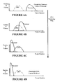
- the graphs of Figures 4A to 4D will be described to provide an overview for an understanding of the purposes of the routine of Figure 3 .
- These graphs show frame rendering performance as a function of CPU and GPU performance, progressively, as relatively increased performance resources are provided to the processor.
- Each graph includes exemplary average distributions of frame duration for the GPU and processor, i.e., the relative times taken by the processor and GPU to generate frame data and rendered frames, respectively.
- the average rendered frame rate increases.
- Figure 4A represents a situation when the frame rate is completely limited by the processor. Moving from graph 4A to 4D, relatively higher performance resources (frequency in this example) are provided to the processor, thereby shifting the processor distribution curve to the left and thus making the overall frame generation rate less limited by the processor. So, it can be seen that if the overall rendered frame rate is processor limited, then it doesn't materially help to increase GPU performance and conversely, when the rendered frame rate is GPU limited, the frame rate is not materially improved by increasing processor performance.
- GPU performance (and not necessarily processor performance) should be increased. If, however, the frame rate is sufficient, then performance resources can be reduced for the processor and thus, power consumption, for example, may be reduced. Likewise, if it is determined that the frame rate may be processor limited, then if the frame rate is not sufficient, it may be inferred that additional performance resources should be provided to the processor. If, however, the frame rate is deemed to be sufficient, then performance resources may be reduced from the GPU. With this in mind, the flow diagram of Figure 3 will be discussed.
- Figure 3 shows a performance allocation engine routine 302 in accordance with some embodiments.
- the graphics render utilization is evaluated. This, for example, could be done by evaluating utilization in a frame rendering engine such as frame rendering utilization 205 in the GPU 105. Utilization is a measure of how hard the rendering engine is working. It may be as simple as whether or not relevant processing units are active or idle, or it could be a more quantitative measure of the extent to which relevant GPU units are performing.
- the rendered frame rate is evaluated (or monitored). This involves determining the rate at which rendered frames are being generated by a frame rendering engine. For example, within the GPU (or even external to it), one or more signals indicative of whether a new frame is being provided to memory (e.g., memory 207) could be monitored to measure or estimate the times between generated frames.
- memory e.g., memory 207
- the frame rate used in the routine may be an instantaneous estimate, an average, a moving average with a desired window size (number of frames), or a combination of such rates.
- a weighted average may be used to filter out anomalies. For example, weight values adding up to one could be employed for different adjacent frame durations to calculate a running average. The number of weight values adding up to one would correspond to the number of frames in the moving window. Depending on the sampling rate used to measure frame durations, the values could be adjusted to achieve acceptable results.
- a first weighting constant, a 1 , of 1/30000 and a second weighting constant, a 2 , of 2999/30000 could be used.
- any suitable or otherwise desired weighting scheme or numbers of frames per window could be utilized.
- the routine determines if GPU utilization is high. If it is not high (e.g., normal or low), then at 310, the routine determines if the rendered frame rate is sufficient. If the frame rate is not sufficient (implying that GPU performance is sufficient but processor performance is insufficient), then at 314, the processor performance may be increased. (Note that a dashed box is used here, and elsewhere in this figure, to indicate that control of the processor performance may not be available to the PAE, so it may either control or otherwise indicate that the processor performance should be increased.) On the other hand, if the frame rate at 310 is sufficient, then at 312, the GPU performance is decreased and additional performance is allocated to the processor. From either 312 or 314, the routine loops back to 304 and 306 as shown.
- the routine proceeds to 316 and determines if the rendered frame rate is sufficient (e.g., in the same way as at 310). If the frame rate is sufficient, then the routine loops back to 304 and 306 and proceeds as discussed. On the other hand, if the frame rate is not sufficient (implying that the frame rate is GPU limited), then at 318, the GPU performance is increased (e.g., frequency is increased), and the routine loops back to 304 and 306 and proceeds as discussed.
- Coupled is used to indicate that two or more elements are in direct physical or electrical contact with each other.
- Connected is used to indicate that two or more elements are in direct physical or electrical contact with each other.
- Connected is used to indicate that two or more elements are in direct physical or electrical contact with each other.
- Connected is used to indicate that two or more elements are in direct physical or electrical contact with each other.
- Connected is used to indicate that two or more elements are in direct physical or electrical contact with each other.
- Coupled is used to indicate that two or more elements co-operate or interact with each other, but they may or may not be in direct physical or electrical contact.
- IC semiconductor integrated circuit
- PDA programmable logic arrays
- signal conductor lines are represented with lines. Some may be thicker, to indicate more constituent signal paths, have a number label, to indicate a number of constituent signal paths, and/or have arrows at one or more ends, to indicate primary information flow direction. This, however, should not be construed in a limiting manner. Rather, such added detail may be used in connection with one or more exemplary embodiments to facilitate easier understanding of a circuit. Any represented signal lines, whether or not having additional information, may actually comprise one or more signals that may travel in multiple directions and may be implemented with any suitable type of signal scheme, e.g., digital or analog lines implemented with differential pairs, optical fiber lines, and/or single-ended lines.
Landscapes
- Engineering & Computer Science (AREA)
- Theoretical Computer Science (AREA)
- General Physics & Mathematics (AREA)
- Physics & Mathematics (AREA)
- General Engineering & Computer Science (AREA)
- Software Systems (AREA)
- Computer Hardware Design (AREA)
- Computer Graphics (AREA)
- Multimedia (AREA)
- Controls And Circuits For Display Device (AREA)
- Power Sources (AREA)
- Image Processing (AREA)
- Testing And Monitoring For Control Systems (AREA)
- Debugging And Monitoring (AREA)
- Image Generation (AREA)
Claims (13)
- Leistungszuweisungsmaschine (107) für die Verwendung in einem System mit einem zentralen Prozessor (102), um eine Anwendung auszuführen und Rahmendaten von der ausgeführten Anwendung zu erzeugen, und einem Graphikprozessor (105) mit einer Rahmenwiedergabemaschine (205), um die Rahmendaten zu empfangen und daraus wiedergegebene Rahmen zu erzeugen, wobei die Leistungszuweisungsmaschine (107) betreibbar ist, eine Rahmenrate, d. h. die Rate, mit der die wiedergegebenen Rahmen durch die Rahmenwiedergabemaschine (205) erzeugt werden, zu überwachen; wobei:die Leistungszuweisungsmaschine (107) auch betreibbar ist, eine Arbeitslast des Graphikprozessors (105) zu überwachen und dem Graphikprozessor (105) und dem zentralen Prozessor (102) Leistungsbetriebsmittel zuzuweisen, so dass dann, wenn (316) die überwachte Rahmenrate unter einer vorgegebenen Rahmenrate liegt, dem Graphikprozessor Leistungsbetriebsmittel zugewiesen werden (318), wenn (308) die überwachte Arbeitslast über einer vorgegebenen Arbeitslast liegt, und umgekehrt dem zentralen Prozessor Leistungsbetriebsmittel zugewiesen werden (314), ohne dem Graphikprozessor Leistungsbetriebsmittel hinzuzufügen, wenn die überwachte Arbeitslast unter der vorgegebenen Arbeitslast liegt.
- Leistungszuweisungsmaschine (107) nach Anspruch 1, wobei die Leistungszuweisungsmaschine (107) betreibbar ist, dem zentralen Prozessor (102) und dem Graphikprozessor (105) Leistungsbetriebsmittel zuzuweisen.
- Leistungszuweisungsmaschine (107) nach Anspruch 2, wobei die Leistungszuweisungsmaschine (107) als ausführbare Anweisungen in einem Graphikprozessortreiber implementiert sind.
- Chip, der die Leistungszuweisungsmaschine (107) nach einem der vorhergehenden Ansprüche 1 bis 3 enthält.
- Rechensystem, das Folgendes umfasst:einen zentralen Prozessor (102), um eine Anwendung auszuführen und Rahmendaten von der ausgeführten Anwendung zu erzeugen;einen Graphikprozessor (105) mit einer Rahmenwiedergabemaschine (205), um die Rahmendaten zu empfangen und daraus wiedergegebene Rahmen zu erzeugen; unddie Leistungszuweisungsmaschine (107) nach einem vorhergehenden Anspruch 1 bis 3.
- System nach Anspruch 5, wobei der zentrale Prozessor (102) mehrere Kerne umfasst, von denen einer oder mehrere dazu dienen, die Rahmendaten zu erzeugen.
- Verfahren, das Folgendes umfasst:Überwachen (304) einer Arbeitslast eines Graphikprozessors (105) mit einer Rahmenwiedergabemaschine (205);Überwachen (306) einer Rahmenrate, d. h. der Rate, mit der die Rahmenwiedergabemaschine (205) des Graphikprozessors (105) Rahmen erzeugt; undZuweisen von Leistungsbetriebsmitteln an den Graphikprozessor und den zentralen Prozessor (102), so dass dann, wenn (316) die überwachte Rahmenrate unter einer vorgegebenen Rahmenrate liegt, dem Graphikprozessor Leistungsbetriebsmittel zugewiesen werden (318), wenn (308) die überwachte Arbeitslast über einer vorgegebenen Arbeitslast liegt, und umgekehrt dem zentralen Prozessor Leistungsbetriebsmittel zugewiesen werden (314), ohne dem Graphikprozessor Leistungsbetriebsmittel hinzuzufügen, wenn die überwachte Arbeitslast unter der vorgegebenen Arbeitslast liegt.
- Verfahren nach Anspruch 7, in dem das Überwachen (304) der Arbeitslast umfasst, zu bestimmen, ob die Rahmenwiedergabeeinheiten (205) in dem Graphikprozessor (105) für einen wesentlichen Zeitbetrag aktiv sind.
- Verfahren nach Anspruch 8, das ferner umfasst, zu bestimmen, ob eine ausreichende Anzahl der Rahmenwiedergabeeinheiten (205) aktiv ist.
- Verfahren nach Anspruch 7, wobei das Überwachen (304) der Arbeitslast umfasst, zu überwachen, ob der Graphikprozessor (105) stillsteht oder nicht.
- Verfahren nach Anspruch 10, das ferner umfasst, einen Stillstands-Betriebs-Zyklus des Graphikprozessors (105) zu bestimmen.
- Verfahren nach Anspruch 7, das umfasst, die Betriebsfrequenz des Graphikprozessors (105) zu verringern (312), wenn (310) die Rahmenrate ausreichend ist und die Arbeitslast genügend gering ist.
- Verfahren nach Anspruch 12, das umfasst, die Betriebsfrequenz des zentralen Prozessors (102) zu erhöhen (318), wenn (310) die Rahmenrate ausreichend ist und die Arbeitslast genügend gering ist.
Applications Claiming Priority (1)
| Application Number | Priority Date | Filing Date | Title |
|---|---|---|---|
| US12/157,479 US8199158B2 (en) | 2008-06-11 | 2008-06-11 | Performance allocation method and apparatus |
Publications (3)
| Publication Number | Publication Date |
|---|---|
| EP2178080A2 EP2178080A2 (de) | 2010-04-21 |
| EP2178080A3 EP2178080A3 (de) | 2010-11-17 |
| EP2178080B1 true EP2178080B1 (de) | 2014-12-17 |
Family
ID=41414320
Family Applications (1)
| Application Number | Title | Priority Date | Filing Date |
|---|---|---|---|
| EP09251531.1A Active EP2178080B1 (de) | 2008-06-11 | 2009-06-11 | Leistungszuweisungsverfahren und -vorrichtung |
Country Status (4)
| Country | Link |
|---|---|
| US (3) | US8199158B2 (de) |
| EP (1) | EP2178080B1 (de) |
| KR (1) | KR101129820B1 (de) |
| CN (2) | CN101609545B (de) |
Families Citing this family (68)
| Publication number | Priority date | Publication date | Assignee | Title |
|---|---|---|---|---|
| US8199158B2 (en) | 2008-06-11 | 2012-06-12 | Intel Corporation | Performance allocation method and apparatus |
| GB0921831D0 (en) | 2009-12-14 | 2010-01-27 | British Telecomm | Graphical data delivery |
| GB201000738D0 (en) | 2010-01-18 | 2010-03-03 | British Telecomm | Graphical data processing |
| US8730251B2 (en) * | 2010-06-07 | 2014-05-20 | Apple Inc. | Switching video streams for a display without a visible interruption |
| US8933948B2 (en) | 2010-10-01 | 2015-01-13 | Apple Inc. | Graphics system which utilizes fine grained analysis to determine performance issues |
| US8462166B2 (en) | 2010-10-01 | 2013-06-11 | Apple Inc. | Graphics system which measures CPU and GPU performance |
| US8527239B2 (en) | 2010-10-01 | 2013-09-03 | Apple Inc. | Automatic detection of performance bottlenecks in a graphics system |
| US8614716B2 (en) | 2010-10-01 | 2013-12-24 | Apple Inc. | Recording a command stream with a rich encoding format for capture and playback of graphics content |
| US8830245B2 (en) * | 2010-12-14 | 2014-09-09 | Amazon Technologies, Inc. | Load balancing between general purpose processors and graphics processors |
| US8922567B2 (en) * | 2011-03-11 | 2014-12-30 | Broadcom Corporation | Regulation of screen composing in a device |
| US8924752B1 (en) | 2011-04-20 | 2014-12-30 | Apple Inc. | Power management for a graphics processing unit or other circuit |
| US9086883B2 (en) * | 2011-06-10 | 2015-07-21 | Qualcomm Incorporated | System and apparatus for consolidated dynamic frequency/voltage control |
| KR20130019674A (ko) * | 2011-08-17 | 2013-02-27 | 삼성전자주식회사 | 단말 및 그 단말에서 어플리케이션 수행 방법 |
| KR101845328B1 (ko) * | 2011-08-22 | 2018-04-04 | 삼성전자 주식회사 | 단말 및 그 단말에서 어플리케이션 수행 방법 |
| US8780120B2 (en) * | 2011-10-02 | 2014-07-15 | Microsoft Corporation | GPU self throttling |
| US9298586B2 (en) | 2011-10-11 | 2016-03-29 | Apple Inc. | Suspending and resuming a graphics application executing on a target device for debugging |
| US8856566B1 (en) | 2011-12-15 | 2014-10-07 | Apple Inc. | Power management scheme that accumulates additional off time for device when no work is available and permits additional power consumption by device when awakened |
| US9304570B2 (en) * | 2011-12-15 | 2016-04-05 | Intel Corporation | Method, apparatus, and system for energy efficiency and energy conservation including power and performance workload-based balancing between multiple processing elements |
| JP5842601B2 (ja) * | 2011-12-26 | 2016-01-13 | 富士通株式会社 | プログラム、情報処理方法及び情報処理装置 |
| KR101229851B1 (ko) * | 2011-12-27 | 2013-02-05 | 한국과학기술원 | 데이터의 병렬적 중복제거 시스템 |
| US9390461B1 (en) | 2012-05-08 | 2016-07-12 | Apple Inc. | Graphics hardware mode controls |
| TW201349167A (zh) * | 2012-05-22 | 2013-12-01 | Hon Hai Prec Ind Co Ltd | 顯卡裝置 |
| US9250665B2 (en) | 2012-06-07 | 2016-02-02 | Apple Inc. | GPU with dynamic performance adjustment |
| KR101472493B1 (ko) * | 2012-06-15 | 2014-12-12 | 건국대학교 산학협력단 | 지피유를 이용한 레인보우 방법 고속 구현 시스템 및 그 방법 |
| EP2880622B1 (de) | 2012-07-31 | 2020-11-04 | Intel Corporation | Hybride darstellungssysteme und verfahren |
| KR20140030823A (ko) * | 2012-09-04 | 2014-03-12 | 삼성전자주식회사 | 3차원 작업 부하를 이용하여 dvfs 정책을 수행하는 시스템-온 칩 및 이의 동작 방법 |
| US9342122B2 (en) | 2012-09-17 | 2016-05-17 | Intel Corporation | Distributing power to heterogeneous compute elements of a processor |
| EP2909696A4 (de) * | 2012-10-16 | 2017-02-22 | Razer (Asia-Pacific) Pte. Ltd. | Computersysteme und verfahren zur steuerung eines computersystems |
| US9269120B2 (en) * | 2012-11-06 | 2016-02-23 | Intel Corporation | Dynamically rebalancing graphics processor resources |
| US9128721B2 (en) * | 2012-12-11 | 2015-09-08 | Apple Inc. | Closed loop CPU performance control |
| US9275601B2 (en) * | 2012-12-12 | 2016-03-01 | Intel Corporation | Techniques to control frame display rate |
| US9195285B2 (en) * | 2012-12-27 | 2015-11-24 | Intel Corporation | Techniques for platform duty cycling |
| US9424620B2 (en) * | 2012-12-29 | 2016-08-23 | Intel Corporation | Identification of GPU phase to determine GPU scalability during runtime |
| KR20140088691A (ko) * | 2013-01-03 | 2014-07-11 | 삼성전자주식회사 | Dvfs 정책을 수행하는 시스템-온 칩 및 이의 동작 방법 |
| US9201487B2 (en) | 2013-03-05 | 2015-12-01 | Intel Corporation | Reducing power consumption during graphics rendering |
| CA2902292C (en) | 2013-03-15 | 2024-05-21 | Ologn Technologies Ag | Systems, methods and apparatuses for securely storing and providing payment information |
| US9378536B2 (en) * | 2014-04-30 | 2016-06-28 | Qualcomm Incorporated | CPU/GPU DCVS co-optimization for reducing power consumption in graphics frame processing |
| US9645916B2 (en) | 2014-05-30 | 2017-05-09 | Apple Inc. | Performance testing for blocks of code |
| CN104932659B (zh) * | 2015-07-15 | 2020-01-07 | 京东方科技集团股份有限公司 | 图像显示方法及显示系统 |
| EP3125072B8 (de) * | 2015-07-29 | 2018-11-14 | Samsung Electronics Co., Ltd. | Verfahren zur stromverwaltung und elektronische vorrichtung |
| GB2540804B (en) * | 2015-07-29 | 2018-03-07 | Samsung Electronics Co Ltd | Hardware power management apparatus and methods |
| CN106708499B (zh) | 2015-11-13 | 2020-10-27 | 财团法人工业技术研究院 | 绘图处理程序的分析方法与分析系统 |
| US9817431B2 (en) * | 2016-02-03 | 2017-11-14 | Qualcomm Incorporated | Frame based clock rate adjustment for processing unit |
| US20170244894A1 (en) * | 2016-02-22 | 2017-08-24 | Seastar Labs, Inc. | Method and Apparatus for Managing Latency of Remote Video Production |
| CN106095047B (zh) * | 2016-05-31 | 2020-07-24 | 联想(北京)有限公司 | 一种控制方法及电子设备 |
| US10331195B2 (en) * | 2016-06-06 | 2019-06-25 | Qualcomm Incorporated | Power and performance aware memory-controller voting mechanism |
| CN106020990B (zh) * | 2016-06-30 | 2020-01-10 | 宇龙计算机通信科技(深圳)有限公司 | 一种中央处理器的控制方法及终端设备 |
| CN106454312A (zh) * | 2016-09-29 | 2017-02-22 | 乐视控股(北京)有限公司 | 一种图像处理方法和装置 |
| US10845865B2 (en) | 2017-04-21 | 2020-11-24 | Intel Corporation | Reducing power consumption when transferring frames from graphics processors to display panels |
| US10504259B2 (en) | 2017-04-24 | 2019-12-10 | Intel Corporation | Separately processing regions or objects or interest from a render engine to a display engine or a display panel |
| US11404023B2 (en) | 2018-03-26 | 2022-08-02 | Huawei Device Co., Ltd. | Frame rate adjustment method and terminal |
| CN108874544A (zh) * | 2018-06-11 | 2018-11-23 | 郑州云海信息技术有限公司 | 一种gpu服务器io资源分配的方法及系统 |
| WO2020062052A1 (en) * | 2018-09-28 | 2020-04-02 | Qualcomm Incorporated | Smart and dynamic janks reduction technology |
| CN109960584A (zh) * | 2019-01-30 | 2019-07-02 | 努比亚技术有限公司 | Cpu调频控制方法、终端及计算机可读存储介质 |
| US12131185B2 (en) * | 2019-05-08 | 2024-10-29 | Telefonaktiebolaget Lm Ericsson (Publ) | Sharing and oversubscription of general-purpose graphical processing units in data centers |
| KR20210097938A (ko) | 2020-01-31 | 2021-08-10 | 에스케이하이닉스 주식회사 | 클록변조를 통해 리드 데이터의 신뢰성을 검증하는 메모리 장치 및 메모리 장치를 포함하는 메모리 시스템 |
| KR102713219B1 (ko) | 2019-09-02 | 2024-10-07 | 에스케이하이닉스 주식회사 | 메모리 컨트롤러 및 그 동작 방법 |
| US12223195B2 (en) | 2019-09-02 | 2025-02-11 | SK Hynix Inc. | Memory controller and operating method thereof |
| CN110532100B (zh) * | 2019-09-02 | 2022-04-15 | Oppo广东移动通信有限公司 | 调度资源的方法、装置、终端及存储介质 |
| US12051470B2 (en) | 2019-09-02 | 2024-07-30 | SK Hynix Inc. | Memory controller and operating method thereof |
| US11501808B2 (en) | 2019-09-02 | 2022-11-15 | SK Hynix Inc. | Memory controller and operating method thereof |
| US11507310B2 (en) | 2019-09-02 | 2022-11-22 | SK Hynix Inc. | Memory controller and operating method thereof |
| KR20210061174A (ko) | 2019-11-19 | 2021-05-27 | 에스케이하이닉스 주식회사 | 메모리 컨트롤러 및 그 동작 방법 |
| KR102862943B1 (ko) * | 2020-02-10 | 2025-09-22 | 삼성전자 주식회사 | 프레임의 생성에 소요된 시간 및 최대 허용 시간에 기반하여 프로세싱 유닛을 제어하는 전자 장치 및 전자 장치의 동작 방법 |
| US11467621B2 (en) * | 2020-02-28 | 2022-10-11 | Qualcomm Incorporated | Computer processing unit intra-frame clock and voltage scaling based on graphics application awareness |
| US12028548B2 (en) * | 2021-04-19 | 2024-07-02 | Synamedia Limited | Rendering video frames for a user interface operation performed at a client device |
| US12333336B2 (en) | 2021-09-24 | 2025-06-17 | Ati Technologies Ulc | Scheduling and clock management for real-time system quality of service (QoS) |
| CN114510406B (zh) * | 2022-02-08 | 2024-07-02 | 北京字节跳动网络技术有限公司 | 检测帧率的方法及相关设备 |
Family Cites Families (26)
| Publication number | Priority date | Publication date | Assignee | Title |
|---|---|---|---|---|
| US7149909B2 (en) * | 2002-05-09 | 2006-12-12 | Intel Corporation | Power management for an integrated graphics device |
| US6950105B2 (en) * | 2002-06-03 | 2005-09-27 | Ati Technologies Inc. | Power consumption management in a video graphics accelerator |
| US7634668B2 (en) * | 2002-08-22 | 2009-12-15 | Nvidia Corporation | Method and apparatus for adaptive power consumption |
| US7268779B2 (en) * | 2002-12-24 | 2007-09-11 | Intel Corporation | Z-buffering techniques for graphics rendering |
| US7119803B2 (en) * | 2002-12-30 | 2006-10-10 | Intel Corporation | Method, apparatus and article for display unit power management |
| US6971034B2 (en) * | 2003-01-09 | 2005-11-29 | Intel Corporation | Power/performance optimized memory controller considering processor power states |
| US7075541B2 (en) | 2003-08-18 | 2006-07-11 | Nvidia Corporation | Adaptive load balancing in a multi-processor graphics processing system |
| US7903116B1 (en) * | 2003-10-27 | 2011-03-08 | Nvidia Corporation | Method, apparatus, and system for adaptive performance level management of a graphics system |
| US7289125B2 (en) * | 2004-02-27 | 2007-10-30 | Nvidia Corporation | Graphics device clustering with PCI-express |
| US7698575B2 (en) * | 2004-03-30 | 2010-04-13 | Intel Corporation | Managing power consumption by requesting an adjustment to an operating point of a processor |
| WO2006034034A2 (en) * | 2004-09-16 | 2006-03-30 | Nvidia Corporation | Load balancing |
| US7898545B1 (en) * | 2004-12-14 | 2011-03-01 | Nvidia Corporation | Apparatus, system, and method for integrated heterogeneous processors |
| US7222253B2 (en) * | 2004-12-28 | 2007-05-22 | Intel Corporation | Dynamic power control for reducing voltage level of graphics controller component of memory controller based on its degree of idleness |
| US7925899B2 (en) * | 2005-12-29 | 2011-04-12 | Intel Corporation | Method, system, and apparatus for runtime power estimation |
| US8102398B2 (en) * | 2006-03-03 | 2012-01-24 | Ati Technologies Ulc | Dynamically controlled power reduction method and circuit for a graphics processor |
| US8314806B2 (en) * | 2006-04-13 | 2012-11-20 | Intel Corporation | Low power display mode |
| US7500041B2 (en) * | 2006-06-15 | 2009-03-03 | Nvidia Corporation | Graphics processing unit for cost effective high performance graphics system with two or more graphics processing units |
| US7412554B2 (en) * | 2006-06-15 | 2008-08-12 | Nvidia Corporation | Bus interface controller for cost-effective high performance graphics system with two or more graphics processing units |
| US8126993B2 (en) * | 2006-07-18 | 2012-02-28 | Nvidia Corporation | System, method, and computer program product for communicating sub-device state information |
| JP2008071261A (ja) | 2006-09-15 | 2008-03-27 | Toshiba Corp | 画像処理システム及び画像処理方法 |
| KR101467558B1 (ko) * | 2007-07-26 | 2014-12-01 | 엘지전자 주식회사 | 그래픽데이터 처리 장치 및 방법 |
| US7711864B2 (en) * | 2007-08-31 | 2010-05-04 | Apple Inc. | Methods and systems to dynamically manage performance states in a data processing system |
| US8458497B2 (en) * | 2007-10-11 | 2013-06-04 | Qualcomm Incorporated | Demand based power control in a graphics processing unit |
| US8243085B2 (en) * | 2007-12-30 | 2012-08-14 | Intel Corporation | Boosting graphics performance based on executing workload |
| US8199158B2 (en) | 2008-06-11 | 2012-06-12 | Intel Corporation | Performance allocation method and apparatus |
| US8386808B2 (en) * | 2008-12-22 | 2013-02-26 | Intel Corporation | Adaptive power budget allocation between multiple components in a computing system |
-
2008
- 2008-06-11 US US12/157,479 patent/US8199158B2/en active Active
-
2009
- 2009-06-10 KR KR1020090051431A patent/KR101129820B1/ko not_active Expired - Fee Related
- 2009-06-11 EP EP09251531.1A patent/EP2178080B1/de active Active
- 2009-06-11 CN CN200910145948.5A patent/CN101609545B/zh active Active
- 2009-06-11 CN CN201310722006.5A patent/CN103927708B/zh active Active
-
2012
- 2012-05-11 US US13/469,395 patent/US8411095B2/en not_active Expired - Fee Related
-
2013
- 2013-02-28 US US13/780,523 patent/US9142001B2/en active Active
Non-Patent Citations (1)
| Title |
|---|
| FLAUTNER K ET AL: "Vertigo: Automatic Performance-Setting for Linux", INTERNET CITATION, 17 May 2002 (2002-05-17), XP002286444, Retrieved from the Internet <URL:http://www.cs.cornell.edu/People/egs/syslunch-fall02/vertigo.pdf> [retrieved on 20040629] * |
Also Published As
| Publication number | Publication date |
|---|---|
| US20090309885A1 (en) | 2009-12-17 |
| CN103927708B (zh) | 2017-07-21 |
| US9142001B2 (en) | 2015-09-22 |
| US8199158B2 (en) | 2012-06-12 |
| CN101609545A (zh) | 2009-12-23 |
| EP2178080A2 (de) | 2010-04-21 |
| CN103927708A (zh) | 2014-07-16 |
| US8411095B2 (en) | 2013-04-02 |
| CN101609545B (zh) | 2014-03-05 |
| KR20090129355A (ko) | 2009-12-16 |
| US20120223954A1 (en) | 2012-09-06 |
| EP2178080A3 (de) | 2010-11-17 |
| US20130229420A1 (en) | 2013-09-05 |
| KR101129820B1 (ko) | 2012-04-13 |
Similar Documents
| Publication | Publication Date | Title |
|---|---|---|
| EP2178080B1 (de) | Leistungszuweisungsverfahren und -vorrichtung | |
| KR101471303B1 (ko) | 그래픽 처리 장치를 위한 전력 관리 장치 및 방법 | |
| US7660247B2 (en) | Dynamic load-based credit distribution | |
| TWI518586B (zh) | 協同處理器與系統效能及電力管理技術 | |
| US9146761B2 (en) | Virtualization system and resource allocation method thereof | |
| RU2573733C1 (ru) | Способ и устройство для регулировки канала i/о на виртуальной платформе | |
| CN105677000B (zh) | 动态电压频率调整的系统及方法 | |
| US20130311815A1 (en) | Providing Adaptive Frequency Control For A Processor | |
| CN103988147B (zh) | 在活动工作负荷期间动态进入低功率状态 | |
| CN108415772B (zh) | 一种基于容器的资源调整方法、装置和介质 | |
| CN105378668A (zh) | 多处理器系统中的操作系统管理的中断引导 | |
| CN110795238A (zh) | 负载计算方法、装置、存储介质及电子设备 | |
| CN107624181B (zh) | 包括虚拟处理器的闲置和调度的虚拟机管理方法和装备 | |
| CN107132903B (zh) | 一种节能管理实现方法、装置及网络设备 | |
| EP4145249B1 (de) | Stromverwaltung von einzelnen lanes einer bus-verbindung | |
| US12481345B2 (en) | Techniques for power management in compute circuits | |
| US9355001B1 (en) | Method and apparatus for selecting an operating frequency of a central processing unit, based on determining a millions of instruction per second (MIPS) value associated with the central processing unit | |
| CN117234744B (zh) | 一种多芯片系统性能优化方法、系统、电子设备及介质 | |
| CN121680595A (zh) | 一种控制方法、装置、设备及存储介质 | |
| CN120994042A (zh) | 数据传输链路的功耗管理方法、装置、芯片及计算机设备 | |
| CN120215677A (zh) | 控制方法、装置、电子设备、芯片及存储介质 |
Legal Events
| Date | Code | Title | Description |
|---|---|---|---|
| PUAI | Public reference made under article 153(3) epc to a published international application that has entered the european phase |
Free format text: ORIGINAL CODE: 0009012 |
|
| 17P | Request for examination filed |
Effective date: 20090701 |
|
| AK | Designated contracting states |
Kind code of ref document: A2 Designated state(s): AT BE BG CH CY CZ DE DK EE ES FI FR GB GR HR HU IE IS IT LI LT LU LV MC MK MT NL NO PL PT RO SE SI SK TR |
|
| AX | Request for extension of the european patent |
Extension state: AL BA RS |
|
| PUAL | Search report despatched |
Free format text: ORIGINAL CODE: 0009013 |
|
| RIC1 | Information provided on ipc code assigned before grant |
Ipc: G09G 5/00 20060101AFI20100317BHEP Ipc: G09G 5/36 20060101ALI20101007BHEP Ipc: G06F 11/34 20060101ALI20101007BHEP |
|
| AK | Designated contracting states |
Kind code of ref document: A3 Designated state(s): AT BE BG CH CY CZ DE DK EE ES FI FR GB GR HR HU IE IS IT LI LT LU LV MC MK MT NL NO PL PT RO SE SI SK TR |
|
| AX | Request for extension of the european patent |
Extension state: AL BA RS |
|
| 17Q | First examination report despatched |
Effective date: 20101102 |
|
| REG | Reference to a national code |
Ref country code: DE Ref legal event code: R079 Ref document number: 602009028353 Country of ref document: DE Free format text: PREVIOUS MAIN CLASS: G09G0005000000 Ipc: G06F0001320000 |
|
| GRAP | Despatch of communication of intention to grant a patent |
Free format text: ORIGINAL CODE: EPIDOSNIGR1 |
|
| RIC1 | Information provided on ipc code assigned before grant |
Ipc: G06F 11/34 20060101ALI20140714BHEP Ipc: G06T 1/00 20060101ALI20140714BHEP Ipc: G09G 5/36 20060101ALI20140714BHEP Ipc: G09G 5/00 20060101ALI20140714BHEP Ipc: G06F 9/50 20060101ALI20140714BHEP Ipc: G06F 1/32 20060101AFI20140714BHEP Ipc: G06T 1/20 20060101ALI20140714BHEP |
|
| INTG | Intention to grant announced |
Effective date: 20140807 |
|
| GRAS | Grant fee paid |
Free format text: ORIGINAL CODE: EPIDOSNIGR3 |
|
| GRAA | (expected) grant |
Free format text: ORIGINAL CODE: 0009210 |
|
| AK | Designated contracting states |
Kind code of ref document: B1 Designated state(s): AT BE BG CH CY CZ DE DK EE ES FI FR GB GR HR HU IE IS IT LI LT LU LV MC MK MT NL NO PL PT RO SE SI SK TR |
|
| REG | Reference to a national code |
Ref country code: GB Ref legal event code: FG4D |
|
| REG | Reference to a national code |
Ref country code: CH Ref legal event code: EP |
|
| REG | Reference to a national code |
Ref country code: IE Ref legal event code: FG4D |
|
| REG | Reference to a national code |
Ref country code: AT Ref legal event code: REF Ref document number: 702334 Country of ref document: AT Kind code of ref document: T Effective date: 20150115 |
|
| REG | Reference to a national code |
Ref country code: DE Ref legal event code: R096 Ref document number: 602009028353 Country of ref document: DE Effective date: 20150129 |
|
| PG25 | Lapsed in a contracting state [announced via postgrant information from national office to epo] |
Ref country code: NO Free format text: LAPSE BECAUSE OF FAILURE TO SUBMIT A TRANSLATION OF THE DESCRIPTION OR TO PAY THE FEE WITHIN THE PRESCRIBED TIME-LIMIT Effective date: 20150317 Ref country code: FI Free format text: LAPSE BECAUSE OF FAILURE TO SUBMIT A TRANSLATION OF THE DESCRIPTION OR TO PAY THE FEE WITHIN THE PRESCRIBED TIME-LIMIT Effective date: 20141217 Ref country code: LT Free format text: LAPSE BECAUSE OF FAILURE TO SUBMIT A TRANSLATION OF THE DESCRIPTION OR TO PAY THE FEE WITHIN THE PRESCRIBED TIME-LIMIT Effective date: 20141217 |
|
| REG | Reference to a national code |
Ref country code: LT Ref legal event code: MG4D |
|
| PG25 | Lapsed in a contracting state [announced via postgrant information from national office to epo] |
Ref country code: SE Free format text: LAPSE BECAUSE OF FAILURE TO SUBMIT A TRANSLATION OF THE DESCRIPTION OR TO PAY THE FEE WITHIN THE PRESCRIBED TIME-LIMIT Effective date: 20141217 Ref country code: GR Free format text: LAPSE BECAUSE OF FAILURE TO SUBMIT A TRANSLATION OF THE DESCRIPTION OR TO PAY THE FEE WITHIN THE PRESCRIBED TIME-LIMIT Effective date: 20150318 Ref country code: LV Free format text: LAPSE BECAUSE OF FAILURE TO SUBMIT A TRANSLATION OF THE DESCRIPTION OR TO PAY THE FEE WITHIN THE PRESCRIBED TIME-LIMIT Effective date: 20141217 Ref country code: HR Free format text: LAPSE BECAUSE OF FAILURE TO SUBMIT A TRANSLATION OF THE DESCRIPTION OR TO PAY THE FEE WITHIN THE PRESCRIBED TIME-LIMIT Effective date: 20141217 |
|
| REG | Reference to a national code |
Ref country code: AT Ref legal event code: MK05 Ref document number: 702334 Country of ref document: AT Kind code of ref document: T Effective date: 20141217 |
|
| PG25 | Lapsed in a contracting state [announced via postgrant information from national office to epo] |
Ref country code: NL Free format text: LAPSE BECAUSE OF FAILURE TO SUBMIT A TRANSLATION OF THE DESCRIPTION OR TO PAY THE FEE WITHIN THE PRESCRIBED TIME-LIMIT Effective date: 20141217 |
|
| PG25 | Lapsed in a contracting state [announced via postgrant information from national office to epo] |
Ref country code: ES Free format text: LAPSE BECAUSE OF FAILURE TO SUBMIT A TRANSLATION OF THE DESCRIPTION OR TO PAY THE FEE WITHIN THE PRESCRIBED TIME-LIMIT Effective date: 20141217 Ref country code: EE Free format text: LAPSE BECAUSE OF FAILURE TO SUBMIT A TRANSLATION OF THE DESCRIPTION OR TO PAY THE FEE WITHIN THE PRESCRIBED TIME-LIMIT Effective date: 20141217 Ref country code: SK Free format text: LAPSE BECAUSE OF FAILURE TO SUBMIT A TRANSLATION OF THE DESCRIPTION OR TO PAY THE FEE WITHIN THE PRESCRIBED TIME-LIMIT Effective date: 20141217 Ref country code: CZ Free format text: LAPSE BECAUSE OF FAILURE TO SUBMIT A TRANSLATION OF THE DESCRIPTION OR TO PAY THE FEE WITHIN THE PRESCRIBED TIME-LIMIT Effective date: 20141217 Ref country code: RO Free format text: LAPSE BECAUSE OF FAILURE TO SUBMIT A TRANSLATION OF THE DESCRIPTION OR TO PAY THE FEE WITHIN THE PRESCRIBED TIME-LIMIT Effective date: 20141217 |
|
| PG25 | Lapsed in a contracting state [announced via postgrant information from national office to epo] |
Ref country code: AT Free format text: LAPSE BECAUSE OF FAILURE TO SUBMIT A TRANSLATION OF THE DESCRIPTION OR TO PAY THE FEE WITHIN THE PRESCRIBED TIME-LIMIT Effective date: 20141217 Ref country code: IS Free format text: LAPSE BECAUSE OF FAILURE TO SUBMIT A TRANSLATION OF THE DESCRIPTION OR TO PAY THE FEE WITHIN THE PRESCRIBED TIME-LIMIT Effective date: 20150417 Ref country code: PL Free format text: LAPSE BECAUSE OF FAILURE TO SUBMIT A TRANSLATION OF THE DESCRIPTION OR TO PAY THE FEE WITHIN THE PRESCRIBED TIME-LIMIT Effective date: 20141217 |
|
| REG | Reference to a national code |
Ref country code: DE Ref legal event code: R097 Ref document number: 602009028353 Country of ref document: DE |
|
| PLBE | No opposition filed within time limit |
Free format text: ORIGINAL CODE: 0009261 |
|
| STAA | Information on the status of an ep patent application or granted ep patent |
Free format text: STATUS: NO OPPOSITION FILED WITHIN TIME LIMIT |
|
| PG25 | Lapsed in a contracting state [announced via postgrant information from national office to epo] |
Ref country code: DK Free format text: LAPSE BECAUSE OF FAILURE TO SUBMIT A TRANSLATION OF THE DESCRIPTION OR TO PAY THE FEE WITHIN THE PRESCRIBED TIME-LIMIT Effective date: 20141217 |
|
| 26N | No opposition filed |
Effective date: 20150918 |
|
| PG25 | Lapsed in a contracting state [announced via postgrant information from national office to epo] |
Ref country code: IT Free format text: LAPSE BECAUSE OF FAILURE TO SUBMIT A TRANSLATION OF THE DESCRIPTION OR TO PAY THE FEE WITHIN THE PRESCRIBED TIME-LIMIT Effective date: 20141217 |
|
| PG25 | Lapsed in a contracting state [announced via postgrant information from national office to epo] |
Ref country code: MC Free format text: LAPSE BECAUSE OF FAILURE TO SUBMIT A TRANSLATION OF THE DESCRIPTION OR TO PAY THE FEE WITHIN THE PRESCRIBED TIME-LIMIT Effective date: 20141217 |
|
| REG | Reference to a national code |
Ref country code: CH Ref legal event code: PL |
|
| PG25 | Lapsed in a contracting state [announced via postgrant information from national office to epo] |
Ref country code: SI Free format text: LAPSE BECAUSE OF FAILURE TO SUBMIT A TRANSLATION OF THE DESCRIPTION OR TO PAY THE FEE WITHIN THE PRESCRIBED TIME-LIMIT Effective date: 20141217 Ref country code: LU Free format text: LAPSE BECAUSE OF FAILURE TO SUBMIT A TRANSLATION OF THE DESCRIPTION OR TO PAY THE FEE WITHIN THE PRESCRIBED TIME-LIMIT Effective date: 20150611 |
|
| REG | Reference to a national code |
Ref country code: IE Ref legal event code: MM4A |
|
| PG25 | Lapsed in a contracting state [announced via postgrant information from national office to epo] |
Ref country code: CH Free format text: LAPSE BECAUSE OF NON-PAYMENT OF DUE FEES Effective date: 20150630 Ref country code: LI Free format text: LAPSE BECAUSE OF NON-PAYMENT OF DUE FEES Effective date: 20150630 Ref country code: IE Free format text: LAPSE BECAUSE OF NON-PAYMENT OF DUE FEES Effective date: 20150611 |
|
| REG | Reference to a national code |
Ref country code: FR Ref legal event code: PLFP Year of fee payment: 8 |
|
| PG25 | Lapsed in a contracting state [announced via postgrant information from national office to epo] |
Ref country code: BE Free format text: LAPSE BECAUSE OF FAILURE TO SUBMIT A TRANSLATION OF THE DESCRIPTION OR TO PAY THE FEE WITHIN THE PRESCRIBED TIME-LIMIT Effective date: 20141217 |
|
| PG25 | Lapsed in a contracting state [announced via postgrant information from national office to epo] |
Ref country code: MT Free format text: LAPSE BECAUSE OF FAILURE TO SUBMIT A TRANSLATION OF THE DESCRIPTION OR TO PAY THE FEE WITHIN THE PRESCRIBED TIME-LIMIT Effective date: 20141217 |
|
| REG | Reference to a national code |
Ref country code: FR Ref legal event code: PLFP Year of fee payment: 9 |
|
| PG25 | Lapsed in a contracting state [announced via postgrant information from national office to epo] |
Ref country code: BG Free format text: LAPSE BECAUSE OF FAILURE TO SUBMIT A TRANSLATION OF THE DESCRIPTION OR TO PAY THE FEE WITHIN THE PRESCRIBED TIME-LIMIT Effective date: 20141217 Ref country code: HU Free format text: LAPSE BECAUSE OF FAILURE TO SUBMIT A TRANSLATION OF THE DESCRIPTION OR TO PAY THE FEE WITHIN THE PRESCRIBED TIME-LIMIT; INVALID AB INITIO Effective date: 20090611 |
|
| PG25 | Lapsed in a contracting state [announced via postgrant information from national office to epo] |
Ref country code: CY Free format text: LAPSE BECAUSE OF FAILURE TO SUBMIT A TRANSLATION OF THE DESCRIPTION OR TO PAY THE FEE WITHIN THE PRESCRIBED TIME-LIMIT Effective date: 20141217 |
|
| PG25 | Lapsed in a contracting state [announced via postgrant information from national office to epo] |
Ref country code: TR Free format text: LAPSE BECAUSE OF FAILURE TO SUBMIT A TRANSLATION OF THE DESCRIPTION OR TO PAY THE FEE WITHIN THE PRESCRIBED TIME-LIMIT Effective date: 20141217 |
|
| REG | Reference to a national code |
Ref country code: FR Ref legal event code: PLFP Year of fee payment: 10 |
|
| PG25 | Lapsed in a contracting state [announced via postgrant information from national office to epo] |
Ref country code: MK Free format text: LAPSE BECAUSE OF FAILURE TO SUBMIT A TRANSLATION OF THE DESCRIPTION OR TO PAY THE FEE WITHIN THE PRESCRIBED TIME-LIMIT Effective date: 20141217 |
|
| PG25 | Lapsed in a contracting state [announced via postgrant information from national office to epo] |
Ref country code: PT Free format text: LAPSE BECAUSE OF FAILURE TO SUBMIT A TRANSLATION OF THE DESCRIPTION OR TO PAY THE FEE WITHIN THE PRESCRIBED TIME-LIMIT Effective date: 20141217 |
|
| P01 | Opt-out of the competence of the unified patent court (upc) registered |
Effective date: 20230518 |
|
| PGFP | Annual fee paid to national office [announced via postgrant information from national office to epo] |
Ref country code: FR Payment date: 20241129 Year of fee payment: 17 |
|
| PGFP | Annual fee paid to national office [announced via postgrant information from national office to epo] |
Ref country code: DE Payment date: 20250521 Year of fee payment: 17 |
|
| PGFP | Annual fee paid to national office [announced via postgrant information from national office to epo] |
Ref country code: GB Payment date: 20250522 Year of fee payment: 17 |