EP2168130B1 - Optical element for x-ray microscopy - Google Patents
Optical element for x-ray microscopy Download PDFInfo
- Publication number
- EP2168130B1 EP2168130B1 EP08773243A EP08773243A EP2168130B1 EP 2168130 B1 EP2168130 B1 EP 2168130B1 EP 08773243 A EP08773243 A EP 08773243A EP 08773243 A EP08773243 A EP 08773243A EP 2168130 B1 EP2168130 B1 EP 2168130B1
- Authority
- EP
- European Patent Office
- Prior art keywords
- monocrystal
- optical axis
- section
- cross
- force
- Prior art date
- Legal status (The legal status is an assumption and is not a legal conclusion. Google has not performed a legal analysis and makes no representation as to the accuracy of the status listed.)
- Not-in-force
Links
Images

Classifications
-
- G—PHYSICS
- G21—NUCLEAR PHYSICS; NUCLEAR ENGINEERING
- G21K—HANDLING OF PARTICLES OR IONISING RADIATION NOT OTHERWISE PROVIDED FOR; IRRADIATION DEVICES; GAMMA RAY OR X-RAY MICROSCOPES
- G21K1/00—Arrangements for handling particles or ionising radiation, e.g. focusing or moderating
- G21K1/06—Arrangements for handling particles or ionising radiation, e.g. focusing or moderating using diffraction, refraction or reflection, e.g. monochromators
-
- G—PHYSICS
- G21—NUCLEAR PHYSICS; NUCLEAR ENGINEERING
- G21K—HANDLING OF PARTICLES OR IONISING RADIATION NOT OTHERWISE PROVIDED FOR; IRRADIATION DEVICES; GAMMA RAY OR X-RAY MICROSCOPES
- G21K7/00—Gamma- or X-ray microscopes
-
- G—PHYSICS
- G21—NUCLEAR PHYSICS; NUCLEAR ENGINEERING
- G21K—HANDLING OF PARTICLES OR IONISING RADIATION NOT OTHERWISE PROVIDED FOR; IRRADIATION DEVICES; GAMMA RAY OR X-RAY MICROSCOPES
- G21K2201/00—Arrangements for handling radiation or particles
- G21K2201/06—Arrangements for handling radiation or particles using diffractive, refractive or reflecting elements
- G21K2201/062—Arrangements for handling radiation or particles using diffractive, refractive or reflecting elements the element being a crystal
-
- G—PHYSICS
- G21—NUCLEAR PHYSICS; NUCLEAR ENGINEERING
- G21K—HANDLING OF PARTICLES OR IONISING RADIATION NOT OTHERWISE PROVIDED FOR; IRRADIATION DEVICES; GAMMA RAY OR X-RAY MICROSCOPES
- G21K2201/00—Arrangements for handling radiation or particles
- G21K2201/06—Arrangements for handling radiation or particles using diffractive, refractive or reflecting elements
- G21K2201/064—Arrangements for handling radiation or particles using diffractive, refractive or reflecting elements having a curved surface
-
- G—PHYSICS
- G21—NUCLEAR PHYSICS; NUCLEAR ENGINEERING
- G21K—HANDLING OF PARTICLES OR IONISING RADIATION NOT OTHERWISE PROVIDED FOR; IRRADIATION DEVICES; GAMMA RAY OR X-RAY MICROSCOPES
- G21K2201/00—Arrangements for handling radiation or particles
- G21K2201/06—Arrangements for handling radiation or particles using diffractive, refractive or reflecting elements
- G21K2201/067—Construction details
Definitions
- Presented solution deals with an X-ray optical element suitable in particular for X-ray microscopy and other X-ray-based display systems.
- X-ray radiation means an electromagnetic radiation with wavelengths shorter than 10 nm.
- X-ray microscopy uses as display elements Fresnel zone plates, biconcave refractive X lenses, polycapillar optics or Göbel mirrors.
- Fresnel zone plates are Fresnel lenses produced by means of electron lithography. Using lithographic methods - but other manufacturing procedures are possible as well - ringlets, or parts of concentric paraboloids, are created in such a way to ensure that radiation emitted from a point on the ringlets' central axis (optical axis), having passed through the ringlets, is focused back again into a point lying on this axis. Thickness of these ringlets or their parts is in orders of tens of nm and their height is roughly 1000 nm. These plates are used as radiation condensers for scanning and display microscopes; in display microscopes they are used also as lenses.
- Fresnel zone plates Another possible way to produce Fresnel zone plates is to create a set of little plates with separate segments containing parallel strips with identical spacing between each other. Diameters of such optical elements are several centimeters as a maximum.
- Biconcave refractive X lenses take the advantage of the fact that the refractive index of certain materials for X-ray radiation is only slightly higher than one and a set of identical cavities, located one after another, creates a condensing lens with long focal distance.
- two crossed systems of biconcave lenses are often used, each focusing the radiation in one direction only. The result is a focusation into a point, which, owing to little differences between the refractive index of the matter and the air, is located in relatively long distance from the lenses - in order of meters.
- Polycapillar optics is created by a set of curved capillaries, which lead the X-ray radiation and focus it into a point.
- Göbel mirrors are plates formed by alternated thin layers of two metals, such as wolfram and silicon, with a shape of part of the surface of elliptic spheroid. These mirrors focus monochromatic X-ray radiation into a point.
- All optical elements described above feature big ratio of focal distance to their diameter, it means relatively long focal distances and small diameters, and their production is costly. They are used in X-ray microscopy for normal as well as so-called scanning microscopes.
- scanning microscopes the beam is focused by the optics into a point on a specimen and a detector senses intensity of X-ray radiation, which has passed through.
- a detector senses intensity of X-ray radiation, which has passed through.
- By measuring all points - which is carried out by shifting the specimen in two mutually orthogonal directions-specimen's final image in given wavelength is obtained.
- JP 06 232015 A The device described in JP 06 232015 A is used for marking the plane orientation of a single crystal ingot, not for focusing X-rays.
- US 5 210 779 A describes a hard X-rays focusing method using dislocation free silicon - germanium crystal, wherein the proportion of germanium and silicon varies over the length of the crystal and change the lattice parameter - we use the stress and shape for focusing X rays.
- US 2003/147161 A1 relates to a method using stress on pheripheral - side surface of the mirror to provide concave or convex deviation on reflective surface of mirror, in order to form errors arising on surface.
- This set-up consists of at least one monocrystal with atomic planes in parallel with optical axis, it means with a line connecting the point to be displayed with the center of its image.
- Mutual distance of the atomic planes in resisting state without the force is d 0 .
- Cross section of the monocrystal is variable.
- the farther and/or closer side of monocristal, which is orthogonal to this optical axis is equipped with a device to create a pull or push force and to maintain a pull or push strength in direction orthogonal to atomic planes of such monocrystal.
- the + sign applies for pull force
- the - sign applies for push force.
- ⁇ is the X-ray radiation wavelength and So is a pre-selected cross section in distance R 0 .
- the optical set-up is formed by minimum two identical monocrystals arranged around the optical axis. All such monocrystals feature equal object and display distance s, while each monocrystal is equipped with a device applying push or pull force F within the minimum distance R 0 from the optical axis and the maximum distance R m from the optical axis. Their cross section is calculated by means of the above-mentioned equation. In other words, it is possible to arrange the monocrystals around the optical axis provided their object and display distances for the same wavelength are equal.
- cross section of the monocrystal's farther side the from the optical axis is bigger than cross section of the monocrystal's closer side to this optical axis, at least one of these sides is equipped with a device creating a pull force between the both sides.
- cross section of the monocrystal's farther side the from the optical axis is smaller than cross section of the monocrystal's closer side to this optical axis, at least one of these sides is equipped with a device creating a push force between the both sides.
- Fig. 1 and 2 show examples of creating two different monocrystals.
- Fig. 3 shows example of basic displaying set-up.
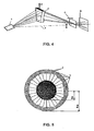
- Fig. 4 shows utilization of the set-up for rotational X-ray scanning microscope.
- Fig. 5 shows a method of creating an optical element from multiple monocrystals and fig. 6 shows its exploitation within a set-up.
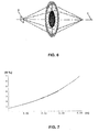
- Fig. 7 shows a chart of dependence of sections ratio S/S 0 on distance from optical axis used for determination of pull force on atomic planes.
- Fig. 1 and 2 show two examples how monocrystal 1 can be created, with designated atomic planes 2 .
- Fig. 1 schematically shows possible shape of monocrystal 1 , an asymmetric shape, designed for shifting the atomic planes by push force.
- Monocrystal's 1 shape in fig. 2 is designed for shifting the atomic planes by pull force. In all cases, the atomic planes 2 where the beam reflects or refracts are horizontal.
- the first example shows a monocrystal 1 where optical axis, i.e. a line connecting a point to be displayed with center of its image, is located under the monocrystal's 1 bigger cross section and the arrow indicates a push force applied by push device.
- optical axis i.e. a line connecting a point to be displayed with center of its image
- Push and pull devices may be implemented in various ways, such as a fixed point and piezo crystal, screw mechanism and tension gauge, etc., and they can be located on one or both opposite sides of monocrystal 1 .
- Fig. 3 shows example of an optical set-up displaying X-ray radiation with wavelength ⁇ .
- This set-up consists of monocrystal 1 with atomic planes 2 , which are arranged in parallel with optical axis 3 .
- Mutual distance of atomic planes 2 in resting state is do and the monocrystal's 1 cross section S is variable.
- the cross section is smaller than on the side closer to the optical axis 3 , and therefore it is equipped with a push device, which is not shown in the figure. Purpose of this push device is to maintain a push force F in direction orthogonal to atomic planes 2 of this monocrystal 1 .
- the figure schematically shows function of symmetrically processed monocrystal 1 , exposed to push force, which focuses X-ray radiation with wavelength ⁇ from distance s to distance s . Both these distances must be equal.
- Monocrystal 1 is located between distances R 0 and R m from optical axis 3 where R 0 is the minimum distance and R m is the maximum distance from optical axis 3 .
- cross section S which is not shown in the figure in order to keep it clear but which can be seen in fig. 1 and 2 , is a function of distance R .
- Cross section S of monocrystal 1 in distance R from optical axis 3 is directly proportional to a pre-selected pull or push force F and indirectly proportional to modulus of elasticity E of given monocrystal 1 in direction of force F in action and depends on distance R and is given by the following formula.
- S S 0 ⁇ R ⁇ R 0 2 + s 2 0.5 - 1 R 0 ⁇ R 2 + s 2 0.5 - 1
- F ⁇ S 0 ⁇ E ⁇ n ⁇ 2 ⁇ R 0 ⁇ d 0 ⁇ R 0 2 + s 2 0.5 - 1
- s with respect to the monocrystal's 1 longitudinal axis, is an object and also a display distance, n is natural number.
- A is the X-ray radiation wavelength and S 0 is a pre-selected cross section of monocrystal 1 upon requirements of the application in distance R 0 from the optical axis 3 .
- Described device is built as follows. Based on used source of X-ray radiation the wavelength A is selected for microscopy as a wavelength, at which the source radiates with maximum intensity, or according to other requirements for application and parameters of monocrystal 1 the object and display distance s and cross section S 0 are selected, for which the force F is calculated for minimum distance R 0 of the monocrystal 1 from optical axis 3 . Subsequently, the dependence of cross section S on distance R is additionally calculated according to the given equation based on calculated force F and modulus of elasticity E . A plate with shape complying with the equation is cut from monocrystal 1. Rays emitted from a point at the object impact the monocrystal 1, reflect from individual atomic planes 2 and are projected in a display plane as shown in fig. 3 .
- single monocrystal 1 may be used, embodied as shown in fig. 4 , where the specimen 5 rotates around axis orthogonal to it, fixed in space, passing through the center of specimen 5 . Such specimen 5 is after each revolution gradually shifted in direction of the arrow, thus allowing its scanning from one end to the other. Intensities of radiation measured by radiation detector 6 are processed by computer into the resulting image similarly as in case of tomography. Simultaneously, this monocrystal 1 acts a monochromator and a separate monochromator may thus be excluded.
- optical set-up may consist of multiple identical monocrystals 1 , which are arranged around the optical axis 3 as shown in fig. 5 . All these monocrystals 1 have equal object and display distance, while each monocrystal 1 is equipped with a device applying on each monocrystal 1 pull force F between the minimum distance R 0 of the bottom side of monocrystals 1 from optical axis 3 and between maximum distance R m from optical axis 3 .
- Their cross section is again calculated according to the given equation. Shape of monocrystals 1 may vary provided their pre-selected cross sections are maintained.
- an optical element consisting of 28 monocrystals 1 where atomic planes 2 act directly as a set-up of concentric polygon ringlets.
- atomic planes 2 act directly as a set-up of concentric polygon ringlets.
- suitable shape and applying suitable force in compliance with the equation it is possible to achieve a situation when among the atomic planes 2 are such distances, which cause the same constructive interference as Fresnel lens for selected wavelength, or possibly also for wavelength, which is half of such wavelength, its third, etc., and act simultaneously as a monochromator, which selects only these wavelengths from the whole spectrum used.
- the same effect may be achieved by using suitable gradient of admixtures in crystal, such as hydrogen in gadolinium, which affects interatomic distance. Implementation of detectors is the same as in other cases.
- Described X-ray optical system exploits properties of spatial grid for focusing monochromatic X-ray radiation from a point source 4 into a point, fig. 6 , or possibly a line segment, fig. 4 , which may be achieved by altering the distance between atomic planes 2 .
- Such shift of atomic planes 2 in monocrystal 1 is created by applying a tension, i.e. pull or push force F , orthogonal to atomic planes 2 , and by suitable selection of cross section S in given height above optical axis 3 , which is calculated using the above-mentioned equation.
- Described element may be used in particular in X-ray microscopy for focusing the X-ray radiation into a line segment.
- an X-ray monochromatic lens for single wavelength may be created, which may serve as a condenser and a monochromator at the same time.
Landscapes
- Physics & Mathematics (AREA)
- Engineering & Computer Science (AREA)
- General Engineering & Computer Science (AREA)
- High Energy & Nuclear Physics (AREA)
- Spectroscopy & Molecular Physics (AREA)
- Analysing Materials By The Use Of Radiation (AREA)
- Crystals, And After-Treatments Of Crystals (AREA)
Abstract
Description
- Presented solution deals with an X-ray optical element suitable in particular for X-ray microscopy and other X-ray-based display systems.
- X-ray radiation means an electromagnetic radiation with wavelengths shorter than 10 nm. Until now, instead of optical lenses used in visible part of light spectrum, X-ray microscopy uses as display elements Fresnel zone plates, biconcave refractive X lenses, polycapillar optics or Göbel mirrors.
- Fresnel zone plates are Fresnel lenses produced by means of electron lithography. Using lithographic methods - but other manufacturing procedures are possible as well - ringlets, or parts of concentric paraboloids, are created in such a way to ensure that radiation emitted from a point on the ringlets' central axis (optical axis), having passed through the ringlets, is focused back again into a point lying on this axis. Thickness of these ringlets or their parts is in orders of tens of nm and their height is roughly 1000 nm. These plates are used as radiation condensers for scanning and display microscopes; in display microscopes they are used also as lenses.
- Another possible way to produce Fresnel zone plates is to create a set of little plates with separate segments containing parallel strips with identical spacing between each other. Diameters of such optical elements are several centimeters as a maximum.
- Biconcave refractive X lenses take the advantage of the fact that the refractive index of certain materials for X-ray radiation is only slightly higher than one and a set of identical cavities, located one after another, creates a condensing lens with long focal distance. In practice, two crossed systems of biconcave lenses are often used, each focusing the radiation in one direction only. The result is a focusation into a point, which, owing to little differences between the refractive index of the matter and the air, is located in relatively long distance from the lenses - in order of meters.
- Polycapillar optics is created by a set of curved capillaries, which lead the X-ray radiation and focus it into a point.
- Göbel mirrors are plates formed by alternated thin layers of two metals, such as wolfram and silicon, with a shape of part of the surface of elliptic spheroid. These mirrors focus monochromatic X-ray radiation into a point.
- All optical elements described above feature big ratio of focal distance to their diameter, it means relatively long focal distances and small diameters, and their production is costly. They are used in X-ray microscopy for normal as well as so-called scanning microscopes. In scanning microscopes, the beam is focused by the optics into a point on a specimen and a detector senses intensity of X-ray radiation, which has passed through. By measuring all points - which is carried out by shifting the specimen in two mutually orthogonal directions-specimen's final image in given wavelength is obtained. Information about intensity of the radiation from the X-ray radiation detectors or digital sensors, such as CCD cameras, which may be used instead of detectors, is led into a computer where the final image is processed.
- All examples described above result in relatively high absorption rate of X-ray radiation and all systems feature also relatively long focal distances, i.e. distances between the display and object, and they can be used for longer wavelengths, around 10 nm. Also, these components impose high demands on production equipment and therefore they are rather expensive.
- There exist also the following documents defining general state of the art, but they do not solve the problem which is subject-matter of this patent application.
- The device described in
JP 06 232015 A -
US 5 210 779 A describes a hard X-rays focusing method using dislocation free silicon - germanium crystal, wherein the proportion of germanium and silicon varies over the length of the crystal and change the lattice parameter - we use the stress and shape for focusing X rays. -
US 2003/147161 A1 relates to a method using stress on pheripheral - side surface of the mirror to provide concave or convex deviation on reflective surface of mirror, in order to form errors arising on surface. - All disadvantages mentioned above are improved by an optical set-up exploiting a monocrystal, which displays X-ray radiation with wavelength λ according to the presented solution. This set-up consists of at least one monocrystal with atomic planes in parallel with optical axis, it means with a line connecting the point to be displayed with the center of its image. Mutual distance of the atomic planes in resisting state without the force is d0. Cross section of the monocrystal is variable. With respect to the optical axis the farther and/or closer side of monocristal, which is orthogonal to this optical axis, is equipped with a device to create a pull or push force and to maintain a pull or push strength in direction orthogonal to atomic planes of such monocrystal. Size of cross section S of the monocrystal under action of pull or push force in distance R from optical axis is directly proportional to pre-selected cross section So and push or pull force F is directly proportional to modulus of elasticity E of given monocrystal in direction of force F in action. Size of the monocrystal's cross section is given by the following formula


- In another possible embodiment, the optical set-up is formed by minimum two identical monocrystals arranged around the optical axis. All such monocrystals feature equal object and display distance s, while each monocrystal is equipped with a device applying push or pull force F within the minimum distance R0 from the optical axis and the maximum distance Rm from the optical axis. Their cross section is calculated by means of the above-mentioned equation. In other words, it is possible to arrange the monocrystals around the optical axis provided their object and display distances for the same wavelength are equal.
- If cross section of the monocrystal's farther side the from the optical axis is bigger than cross section of the monocrystal's closer side to this optical axis, at least one of these sides is equipped with a device creating a pull force between the both sides. On the contrary, if cross section of the monocrystal's farther side the from the optical axis is smaller than cross section of the monocrystal's closer side to this optical axis, at least one of these sides is equipped with a device creating a push force between the both sides.
- Advantage of this solution is relatively simple production of its components, which is based on Hooke's law without needing to know the exact position of individual atomic planes. Production of current Fresnel structures involves electron lithography for individual ringlets, while this method requires only precise machining of the outer shape, for instance cutting by water jet or laser, and applying a force, which can be controlled. Machining of the outer shape results in better physical effect, it means lower absorption and larger active area, with lower costs because lithography is significantly more expensive than cutting. Another advantage is that it works for also for lower order wavelengths, i.e. below 1 nm.
- Example of a displaying optical set-up according to the presented solution is shown in attached drawings.
Fig. 1 and 2 show examples of creating two different monocrystals.Fig. 3 shows example of basic displaying set-up.Fig. 4 shows utilization of the set-up for rotational X-ray scanning microscope.Fig. 5 shows a method of creating an optical element from multiple monocrystals andfig. 6 shows its exploitation within a set-up.Fig. 7 shows a chart of dependence of sections ratio S/S0 on distance from optical axis used for determination of pull force on atomic planes. -
Fig. 1 and 2 show two examples how monocrystal 1 can be created, with designatedatomic planes 2.Fig. 1 schematically shows possible shape ofmonocrystal 1, an asymmetric shape, designed for shifting the atomic planes by push force. Monocrystal's 1 shape infig. 2 is designed for shifting the atomic planes by pull force. In all cases, theatomic planes 2 where the beam reflects or refracts are horizontal. The first example shows amonocrystal 1 where optical axis, i.e. a line connecting a point to be displayed with center of its image, is located under the monocrystal's 1 bigger cross section and the arrow indicates a push force applied by push device. On the contrary,fig. 2 shows situation when the monocrystal's 1 imaginary optical axis is located under the monocrystal's 1 smaller cross section and the arrow indicates a pull force applied by pull device. Push and pull devices may be implemented in various ways, such as a fixed point and piezo crystal, screw mechanism and tension gauge, etc., and they can be located on one or both opposite sides ofmonocrystal 1. -
Fig. 3 shows example of an optical set-up displaying X-ray radiation with wavelength λ. This set-up consists ofmonocrystal 1 withatomic planes 2, which are arranged in parallel withoptical axis 3. Mutual distance ofatomic planes 2 in resting state is do and the monocrystal's 1 cross section S is variable. On the farther side ofmonocrystal 1 from theoptical axis 3, orthogonal to thisoptical axis 3, the cross section is smaller than on the side closer to theoptical axis 3, and therefore it is equipped with a push device, which is not shown in the figure. Purpose of this push device is to maintain a push force F in direction orthogonal toatomic planes 2 of thismonocrystal 1. - The figure schematically shows function of symmetrically processed
monocrystal 1, exposed to push force, which focuses X-ray radiation with wavelength λ from distance s to distance s. Both these distances must be equal.Monocrystal 1 is located between distances R 0 and R m fromoptical axis 3 where R 0 is the minimum distance and R m is the maximum distance fromoptical axis 3. Based on given equation, cross section S, which is not shown in the figure in order to keep it clear but which can be seen infig. 1 and 2 , is a function of distance R. - Cross section S of
monocrystal 1 in distance R fromoptical axis 3 is directly proportional to a pre-selected pull or push force F and indirectly proportional to modulus of elasticity E of givenmonocrystal 1 in direction of force F in action and depends on distance R and is given by the following formula.

monocrystal 1, while value of S will always be positive. A is the X-ray radiation wavelength and S 0 is a pre-selected cross section ofmonocrystal 1 upon requirements of the application in distance R 0 from theoptical axis 3. - Described device is built as follows. Based on used source of X-ray radiation the wavelength A is selected for microscopy as a wavelength, at which the source radiates with maximum intensity, or according to other requirements for application and parameters of
monocrystal 1 the object and display distance s and cross section S 0 are selected, for which the force F is calculated for minimum distance R 0 of themonocrystal 1 fromoptical axis 3. Subsequently, the dependence of cross section S on distance R is additionally calculated according to the given equation based on calculated force F and modulus of elasticity E. A plate with shape complying with the equation is cut frommonocrystal 1. Rays emitted from a point at the object impact themonocrystal 1, reflect from individualatomic planes 2 and are projected in a display plane as shown infig. 3 . - In case of rotating X-ray scanning microscope with a
source 4 of X-ray radiation,single monocrystal 1 may be used, embodied as shown infig. 4 , where thespecimen 5 rotates around axis orthogonal to it, fixed in space, passing through the center ofspecimen 5.Such specimen 5 is after each revolution gradually shifted in direction of the arrow, thus allowing its scanning from one end to the other. Intensities of radiation measured byradiation detector 6 are processed by computer into the resulting image similarly as in case of tomography. Simultaneously, thismonocrystal 1 acts a monochromator and a separate monochromator may thus be excluded. - As shown in
fig. 6 , optical set-up may consist of multipleidentical monocrystals 1, which are arranged around theoptical axis 3 as shown infig. 5 . All thesemonocrystals 1 have equal object and display distance, while eachmonocrystal 1 is equipped with a device applying on eachmonocrystal 1 pull force F between the minimum distance R 0 of the bottom side ofmonocrystals 1 fromoptical axis 3 and between maximum distance R m fromoptical axis 3. Their cross section is again calculated according to the given equation. Shape ofmonocrystals 1 may vary provided their pre-selected cross sections are maintained. In this case, as an example, an optical element consisting of 28monocrystals 1 is shown, whereatomic planes 2 act directly as a set-up of concentric polygon ringlets. By selecting suitable shape and applying suitable force in compliance with the equation it is possible to achieve a situation when among theatomic planes 2 are such distances, which cause the same constructive interference as Fresnel lens for selected wavelength, or possibly also for wavelength, which is half of such wavelength, its third, etc., and act simultaneously as a monochromator, which selects only these wavelengths from the whole spectrum used. The same effect may be achieved by using suitable gradient of admixtures in crystal, such as hydrogen in gadolinium, which affects interatomic distance. Implementation of detectors is the same as in other cases. -
Fig. 7 shows chart with dependencies of sections ratios S/S0 ofmonocrystal 1 on distance fromoptical axis 3 used for determination of pull force onatomic planes 2 for the following values: λ = 0.1 nm, do = 0.4 nm, R0 = 0.01 m, s = 0.5 m and n = 1, in the extent up to Rmax = 0,07 m. - Described X-ray optical system exploits properties of spatial grid for focusing monochromatic X-ray radiation from a
point source 4 into a point,fig. 6 , or possibly a line segment,fig. 4 , which may be achieved by altering the distance betweenatomic planes 2. Such shift ofatomic planes 2 inmonocrystal 1 is created by applying a tension, i.e. pull or push force F, orthogonal toatomic planes 2, and by suitable selection of cross section S in given height aboveoptical axis 3, which is calculated using the above-mentioned equation. - Described element may be used in particular in X-ray microscopy for focusing the X-ray radiation into a line segment. By arranging multiple pieces, an X-ray monochromatic lens for single wavelength may be created, which may serve as a condenser and a monochromator at the same time.
Claims (4)
- Optical set-up arrangeable for displaying X-ray radiation of wavelength λ such that the object distance s of a point to be displayed equals its image distance s, the point to be displayed with the center of its image defining an optical axis,
the optical set-up comprising
at least one monocrystal (1) with variable cross section S and with atomic planes (2), the monocrystal being arranged such that said atomic planes are in parallel with optical axis (3), and
a device for creating and maintaining pull or push force F in direction orthogonal to said atomic planes (2) arranged at that side of the monocrystal (1) that is farther from the optical axis and/or at that side of the monocrystal (1) that is closer to the optical axis (3), where under the action of the pull or push force, the size of the cross section S of the monocrystal (1) at a distance R from the optical axis (3) is directly proportional to the pull or push force F and to the cross section Sθ at the distance Rθ from the optical axis (3), and is indirectly proportional to the modulus ef elasticity E of the monocrystal (1) in the direction of the force F,
and wherein the variable cross section S of the least one monocrystal is given by the formula
and the device for creating and maintaining the pull or push force is arranged to apply a force F given by the formula
Where n is natural number, do is the mutual distance of said atomic planes in the resting state, and the plus sign applies for a pull force and the minus sign applies for a push force. - Optical set-up according to claim 1 comprising a minimum two monocrystals (1), wherein all of these monocrystals (1) are arranged around the optical axis (3) and wherein each monocrystal (1) is equipped with at least one device for applying and maintaining pull or push force F
- Optical set-up according to claims 1 or 2 characterized by the fact that the cross section of the side of the monocrystal (1) that is farther from the optical axis (3) is bigger than the cross section of that side of the monocrystal (1) that is closer to this optical axis (3), and by the fact that at least one of these sides is equipped with a device arranged for creating a pull force between the both sides.
- Optical set-up according to claims 1 or 2 characterized by the fact that the cross section of the side of the monocrystal (1) that is farther from the optical axis (3) is smaller than the cross section of that side of the monocrystal (1) that is closer to this optical axis (3), and by the fact that at least one of these sides is equipped with a device arranged for creating a push force between the both sides.
Applications Claiming Priority (2)
| Application Number | Priority Date | Filing Date | Title |
|---|---|---|---|
| CZ20070494A CZ299759B6 (en) | 2007-07-20 | 2007-07-20 | Optical element for X-ray microscopy |
| PCT/CZ2008/000072 WO2009012732A2 (en) | 2007-07-20 | 2008-06-19 | Optical element for x-ray microscopy |
Publications (2)
| Publication Number | Publication Date |
|---|---|
| EP2168130A2 EP2168130A2 (en) | 2010-03-31 |
| EP2168130B1 true EP2168130B1 (en) | 2012-06-06 |
Family
ID=39941697
Family Applications (1)
| Application Number | Title | Priority Date | Filing Date |
|---|---|---|---|
| EP08773243A Not-in-force EP2168130B1 (en) | 2007-07-20 | 2008-06-19 | Optical element for x-ray microscopy |
Country Status (3)
| Country | Link |
|---|---|
| EP (1) | EP2168130B1 (en) |
| CZ (1) | CZ299759B6 (en) |
| WO (1) | WO2009012732A2 (en) |
Families Citing this family (1)
| Publication number | Priority date | Publication date | Assignee | Title |
|---|---|---|---|---|
| EP3999069B1 (en) * | 2019-07-18 | 2023-10-11 | ENYO Pharma | Synergistic effect of eyp001 and pegylated ifn-alpha for the treatment of hbv infection |
Family Cites Families (6)
| Publication number | Priority date | Publication date | Assignee | Title |
|---|---|---|---|---|
| US5210779A (en) * | 1991-07-26 | 1993-05-11 | Hughes Aircraft Company | Apparatus and method for focusing hard x-rays |
| JP3412852B2 (en) * | 1993-02-04 | 2003-06-03 | 理学電機株式会社 | Single crystal ingot marking device |
| JPH1010299A (en) * | 1996-06-26 | 1998-01-16 | Ishikawajima Harima Heavy Ind Co Ltd | Asymmetric square spectrometer |
| JP3741398B2 (en) * | 1997-08-29 | 2006-02-01 | 株式会社リガク | X-ray measuring method and X-ray measuring apparatus |
| US6389100B1 (en) * | 1999-04-09 | 2002-05-14 | Osmic, Inc. | X-ray lens system |
| JP2003234269A (en) * | 2002-02-07 | 2003-08-22 | Nikon Corp | Method for holding reflection mirror, holding member for reflection mirror, and exposure apparatus |
-
2007
- 2007-07-20 CZ CZ20070494A patent/CZ299759B6/en not_active IP Right Cessation
-
2008
- 2008-06-19 WO PCT/CZ2008/000072 patent/WO2009012732A2/en not_active Ceased
- 2008-06-19 EP EP08773243A patent/EP2168130B1/en not_active Not-in-force
Also Published As
| Publication number | Publication date |
|---|---|
| CZ2007494A3 (en) | 2008-11-12 |
| CZ299759B6 (en) | 2008-11-12 |
| WO2009012732A2 (en) | 2009-01-29 |
| WO2009012732A3 (en) | 2009-06-18 |
| WO2009012732A4 (en) | 2009-08-20 |
| EP2168130A2 (en) | 2010-03-31 |
Similar Documents
| Publication | Publication Date | Title |
|---|---|---|
| Evans-Lutterodt et al. | Single-element elliptical hard x-ray micro-optics | |
| Petrov et al. | Polymer X-ray refractive nano-lenses fabricated by additive technology | |
| Liu et al. | Demonstration of achromatic cold-neutron microscope utilizing axisymmetric focusing mirrors | |
| JP2013210377A (en) | Beam adjustment system | |
| WO1988001428A1 (en) | Instrumentation for conditioning x-ray or neutron beams | |
| Cornelius et al. | In situ three-dimensional reciprocal-space mapping during mechanical deformation | |
| Karvinen et al. | Kinoform diffractive lenses for efficient nano-focusing of hard X-rays | |
| Thiel et al. | Production of intense micrometer‐sized x‐ray beams with tapered glass monocapillaries | |
| Sanli et al. | Apochromatic X-ray focusing | |
| JP5942190B2 (en) | Oblique-incidence X-ray imaging optical device using double reflection type X-ray mirror | |
| JP3597044B2 (en) | Cold neutron focusing device | |
| Fox et al. | Nanofocusing optics for synchrotron radiation made from polycrystalline diamond | |
| Seiboth et al. | Hard x-ray nanofocusing by refractive lenses of constant thickness | |
| CN103559927A (en) | Hard X-ray focusing optical component for eliminating spherical aberration and design method thereof | |
| CN117079856A (en) | Hard X-ray micro-focusing Nb/Al multilayer film Laue lens | |
| US6863409B2 (en) | Apparatus for generating parallel beam with high flux | |
| Heilmann et al. | Fabrication and performance of blazed transmission gratings for x-ray astronomy | |
| CN103559926B (en) | A kind of phase place flap-type nano-focusing unit and method for designing thereof | |
| EP2168130A2 (en) | Optical element for x-ray microscopy | |
| Basov et al. | Two-dimensional focusing of hard X-rays by a phase circular Bragg-Fresnel lens in the case of Bragg backscattering | |
| Prasciolu et al. | On the use of multilayer Laue lenses with X-ray free electron lasers | |
| Snigireva et al. | High‐Energy Nanoscale‐Resolution X‐ray Microscopy Based on Refractive Optics on a Long Beamline | |
| CN113874961A (en) | Stabilized grating structure | |
| Ishikawa et al. | 12-inch X-ray optics based on MEMS process | |
| Tomie | The birth of the X-ray refractive lens |
Legal Events
| Date | Code | Title | Description |
|---|---|---|---|
| PUAI | Public reference made under article 153(3) epc to a published international application that has entered the european phase |
Free format text: ORIGINAL CODE: 0009012 |
|
| 17P | Request for examination filed |
Effective date: 20091209 |
|
| AK | Designated contracting states |
Kind code of ref document: A2 Designated state(s): AT BE BG CH CY CZ DE DK EE ES FI FR GB GR HR HU IE IS IT LI LT LU LV MC MT NL NO PL PT RO SE SI SK TR |
|
| AX | Request for extension of the european patent |
Extension state: AL BA MK RS |
|
| 17Q | First examination report despatched |
Effective date: 20100525 |
|
| GRAP | Despatch of communication of intention to grant a patent |
Free format text: ORIGINAL CODE: EPIDOSNIGR1 |
|
| DAX | Request for extension of the european patent (deleted) | ||
| GRAS | Grant fee paid |
Free format text: ORIGINAL CODE: EPIDOSNIGR3 |
|
| RAP1 | Party data changed (applicant data changed or rights of an application transferred) |
Owner name: CESKE VYSOKE UCENI TECHNICKE V PRAZE |
|
| GRAA | (expected) grant |
Free format text: ORIGINAL CODE: 0009210 |
|
| AK | Designated contracting states |
Kind code of ref document: B1 Designated state(s): AT BE BG CH CY CZ DE DK EE ES FI FR GB GR HR HU IE IS IT LI LT LU LV MC MT NL NO PL PT RO SE SI SK TR |
|
| REG | Reference to a national code |
Ref country code: GB Ref legal event code: FG4D |
|
| REG | Reference to a national code |
Ref country code: AT Ref legal event code: REF Ref document number: 561368 Country of ref document: AT Kind code of ref document: T Effective date: 20120615 Ref country code: CH Ref legal event code: EP |
|
| REG | Reference to a national code |
Ref country code: IE Ref legal event code: FG4D |
|
| RIN2 | Information on inventor provided after grant (corrected) |
Inventor name: CHADZITASKOS, GOCE |
|
| REG | Reference to a national code |
Ref country code: DE Ref legal event code: R096 Ref document number: 602008016204 Country of ref document: DE Effective date: 20120802 |
|
| REG | Reference to a national code |
Ref country code: NL Ref legal event code: VDEP Effective date: 20120606 |
|
| PG25 | Lapsed in a contracting state [announced via postgrant information from national office to epo] |
Ref country code: FI Free format text: LAPSE BECAUSE OF FAILURE TO SUBMIT A TRANSLATION OF THE DESCRIPTION OR TO PAY THE FEE WITHIN THE PRESCRIBED TIME-LIMIT Effective date: 20120606 Ref country code: NO Free format text: LAPSE BECAUSE OF FAILURE TO SUBMIT A TRANSLATION OF THE DESCRIPTION OR TO PAY THE FEE WITHIN THE PRESCRIBED TIME-LIMIT Effective date: 20120906 Ref country code: LT Free format text: LAPSE BECAUSE OF FAILURE TO SUBMIT A TRANSLATION OF THE DESCRIPTION OR TO PAY THE FEE WITHIN THE PRESCRIBED TIME-LIMIT Effective date: 20120606 Ref country code: SE Free format text: LAPSE BECAUSE OF FAILURE TO SUBMIT A TRANSLATION OF THE DESCRIPTION OR TO PAY THE FEE WITHIN THE PRESCRIBED TIME-LIMIT Effective date: 20120606 Ref country code: CY Free format text: LAPSE BECAUSE OF FAILURE TO SUBMIT A TRANSLATION OF THE DESCRIPTION OR TO PAY THE FEE WITHIN THE PRESCRIBED TIME-LIMIT Effective date: 20120606 |
|
| REG | Reference to a national code |
Ref country code: AT Ref legal event code: MK05 Ref document number: 561368 Country of ref document: AT Kind code of ref document: T Effective date: 20120606 |
|
| REG | Reference to a national code |
Ref country code: LT Ref legal event code: MG4D Effective date: 20120606 |
|
| PG25 | Lapsed in a contracting state [announced via postgrant information from national office to epo] |
Ref country code: SI Free format text: LAPSE BECAUSE OF FAILURE TO SUBMIT A TRANSLATION OF THE DESCRIPTION OR TO PAY THE FEE WITHIN THE PRESCRIBED TIME-LIMIT Effective date: 20120606 Ref country code: GR Free format text: LAPSE BECAUSE OF FAILURE TO SUBMIT A TRANSLATION OF THE DESCRIPTION OR TO PAY THE FEE WITHIN THE PRESCRIBED TIME-LIMIT Effective date: 20120907 Ref country code: HR Free format text: LAPSE BECAUSE OF FAILURE TO SUBMIT A TRANSLATION OF THE DESCRIPTION OR TO PAY THE FEE WITHIN THE PRESCRIBED TIME-LIMIT Effective date: 20120606 Ref country code: LV Free format text: LAPSE BECAUSE OF FAILURE TO SUBMIT A TRANSLATION OF THE DESCRIPTION OR TO PAY THE FEE WITHIN THE PRESCRIBED TIME-LIMIT Effective date: 20120606 |
|
| PG25 | Lapsed in a contracting state [announced via postgrant information from national office to epo] |
Ref country code: BE Free format text: LAPSE BECAUSE OF FAILURE TO SUBMIT A TRANSLATION OF THE DESCRIPTION OR TO PAY THE FEE WITHIN THE PRESCRIBED TIME-LIMIT Effective date: 20120606 Ref country code: IS Free format text: LAPSE BECAUSE OF FAILURE TO SUBMIT A TRANSLATION OF THE DESCRIPTION OR TO PAY THE FEE WITHIN THE PRESCRIBED TIME-LIMIT Effective date: 20121006 Ref country code: CZ Free format text: LAPSE BECAUSE OF FAILURE TO SUBMIT A TRANSLATION OF THE DESCRIPTION OR TO PAY THE FEE WITHIN THE PRESCRIBED TIME-LIMIT Effective date: 20120606 Ref country code: RO Free format text: LAPSE BECAUSE OF FAILURE TO SUBMIT A TRANSLATION OF THE DESCRIPTION OR TO PAY THE FEE WITHIN THE PRESCRIBED TIME-LIMIT Effective date: 20120606 Ref country code: SK Free format text: LAPSE BECAUSE OF FAILURE TO SUBMIT A TRANSLATION OF THE DESCRIPTION OR TO PAY THE FEE WITHIN THE PRESCRIBED TIME-LIMIT Effective date: 20120606 Ref country code: MC Free format text: LAPSE BECAUSE OF NON-PAYMENT OF DUE FEES Effective date: 20120630 Ref country code: AT Free format text: LAPSE BECAUSE OF FAILURE TO SUBMIT A TRANSLATION OF THE DESCRIPTION OR TO PAY THE FEE WITHIN THE PRESCRIBED TIME-LIMIT Effective date: 20120606 Ref country code: EE Free format text: LAPSE BECAUSE OF FAILURE TO SUBMIT A TRANSLATION OF THE DESCRIPTION OR TO PAY THE FEE WITHIN THE PRESCRIBED TIME-LIMIT Effective date: 20120606 Ref country code: NL Free format text: LAPSE BECAUSE OF FAILURE TO SUBMIT A TRANSLATION OF THE DESCRIPTION OR TO PAY THE FEE WITHIN THE PRESCRIBED TIME-LIMIT Effective date: 20120606 |
|
| REG | Reference to a national code |
Ref country code: CH Ref legal event code: PL |
|
| REG | Reference to a national code |
Ref country code: CH Ref legal event code: PL |
|
| PG25 | Lapsed in a contracting state [announced via postgrant information from national office to epo] |
Ref country code: PT Free format text: LAPSE BECAUSE OF FAILURE TO SUBMIT A TRANSLATION OF THE DESCRIPTION OR TO PAY THE FEE WITHIN THE PRESCRIBED TIME-LIMIT Effective date: 20121008 Ref country code: IT Free format text: LAPSE BECAUSE OF FAILURE TO SUBMIT A TRANSLATION OF THE DESCRIPTION OR TO PAY THE FEE WITHIN THE PRESCRIBED TIME-LIMIT Effective date: 20120606 Ref country code: PL Free format text: LAPSE BECAUSE OF FAILURE TO SUBMIT A TRANSLATION OF THE DESCRIPTION OR TO PAY THE FEE WITHIN THE PRESCRIBED TIME-LIMIT Effective date: 20120606 |
|
| PGFP | Annual fee paid to national office [announced via postgrant information from national office to epo] |
Ref country code: GB Payment date: 20121031 Year of fee payment: 5 |
|
| REG | Reference to a national code |
Ref country code: IE Ref legal event code: MM4A |
|
| PLBE | No opposition filed within time limit |
Free format text: ORIGINAL CODE: 0009261 |
|
| STAA | Information on the status of an ep patent application or granted ep patent |
Free format text: STATUS: NO OPPOSITION FILED WITHIN TIME LIMIT |
|
| PG25 | Lapsed in a contracting state [announced via postgrant information from national office to epo] |
Ref country code: DK Free format text: LAPSE BECAUSE OF FAILURE TO SUBMIT A TRANSLATION OF THE DESCRIPTION OR TO PAY THE FEE WITHIN THE PRESCRIBED TIME-LIMIT Effective date: 20120606 Ref country code: CH Free format text: LAPSE BECAUSE OF NON-PAYMENT OF DUE FEES Effective date: 20120630 Ref country code: LI Free format text: LAPSE BECAUSE OF NON-PAYMENT OF DUE FEES Effective date: 20120630 Ref country code: IE Free format text: LAPSE BECAUSE OF NON-PAYMENT OF DUE FEES Effective date: 20120619 Ref country code: ES Free format text: LAPSE BECAUSE OF FAILURE TO SUBMIT A TRANSLATION OF THE DESCRIPTION OR TO PAY THE FEE WITHIN THE PRESCRIBED TIME-LIMIT Effective date: 20120917 |
|
| 26N | No opposition filed |
Effective date: 20130307 |
|
| REG | Reference to a national code |
Ref country code: DE Ref legal event code: R097 Ref document number: 602008016204 Country of ref document: DE Effective date: 20130307 |
|
| PG25 | Lapsed in a contracting state [announced via postgrant information from national office to epo] |
Ref country code: BG Free format text: LAPSE BECAUSE OF FAILURE TO SUBMIT A TRANSLATION OF THE DESCRIPTION OR TO PAY THE FEE WITHIN THE PRESCRIBED TIME-LIMIT Effective date: 20120906 Ref country code: MT Free format text: LAPSE BECAUSE OF FAILURE TO SUBMIT A TRANSLATION OF THE DESCRIPTION OR TO PAY THE FEE WITHIN THE PRESCRIBED TIME-LIMIT Effective date: 20120606 |
|
| GBPC | Gb: european patent ceased through non-payment of renewal fee |
Effective date: 20130619 |
|
| PG25 | Lapsed in a contracting state [announced via postgrant information from national office to epo] |
Ref country code: GB Free format text: LAPSE BECAUSE OF NON-PAYMENT OF DUE FEES Effective date: 20130619 Ref country code: TR Free format text: LAPSE BECAUSE OF FAILURE TO SUBMIT A TRANSLATION OF THE DESCRIPTION OR TO PAY THE FEE WITHIN THE PRESCRIBED TIME-LIMIT Effective date: 20120606 |
|
| PG25 | Lapsed in a contracting state [announced via postgrant information from national office to epo] |
Ref country code: LU Free format text: LAPSE BECAUSE OF NON-PAYMENT OF DUE FEES Effective date: 20120619 |
|
| PG25 | Lapsed in a contracting state [announced via postgrant information from national office to epo] |
Ref country code: HU Free format text: LAPSE BECAUSE OF FAILURE TO SUBMIT A TRANSLATION OF THE DESCRIPTION OR TO PAY THE FEE WITHIN THE PRESCRIBED TIME-LIMIT Effective date: 20080619 |
|
| REG | Reference to a national code |
Ref country code: FR Ref legal event code: PLFP Year of fee payment: 8 |
|
| REG | Reference to a national code |
Ref country code: FR Ref legal event code: PLFP Year of fee payment: 9 |
|
| REG | Reference to a national code |
Ref country code: FR Ref legal event code: PLFP Year of fee payment: 10 |
|
| REG | Reference to a national code |
Ref country code: FR Ref legal event code: PLFP Year of fee payment: 11 |
|
| PGFP | Annual fee paid to national office [announced via postgrant information from national office to epo] |
Ref country code: DE Payment date: 20180516 Year of fee payment: 11 |
|
| PGFP | Annual fee paid to national office [announced via postgrant information from national office to epo] |
Ref country code: FR Payment date: 20180516 Year of fee payment: 11 |
|
| REG | Reference to a national code |
Ref country code: DE Ref legal event code: R119 Ref document number: 602008016204 Country of ref document: DE |
|
| PG25 | Lapsed in a contracting state [announced via postgrant information from national office to epo] |
Ref country code: DE Free format text: LAPSE BECAUSE OF NON-PAYMENT OF DUE FEES Effective date: 20200101 |
|
| PG25 | Lapsed in a contracting state [announced via postgrant information from national office to epo] |
Ref country code: FR Free format text: LAPSE BECAUSE OF NON-PAYMENT OF DUE FEES Effective date: 20190630 |