EP2159604B1 - Strahlungsbildwandler - Google Patents
Strahlungsbildwandler Download PDFInfo
- Publication number
- EP2159604B1 EP2159604B1 EP08022501.4A EP08022501A EP2159604B1 EP 2159604 B1 EP2159604 B1 EP 2159604B1 EP 08022501 A EP08022501 A EP 08022501A EP 2159604 B1 EP2159604 B1 EP 2159604B1
- Authority
- EP
- European Patent Office
- Prior art keywords
- film
- radiation
- main surface
- film thickness
- converting
- Prior art date
- Legal status (The legal status is an assumption and is not a legal conclusion. Google has not performed a legal analysis and makes no representation as to the accuracy of the status listed.)
- Active
Links
Images


Classifications
-
- G—PHYSICS
- G01—MEASURING; TESTING
- G01T—MEASUREMENT OF NUCLEAR OR X-RADIATION
- G01T1/00—Measuring X-radiation, gamma radiation, corpuscular radiation, or cosmic radiation
- G01T1/16—Measuring radiation intensity
- G01T1/20—Measuring radiation intensity with scintillation detectors
- G01T1/202—Measuring radiation intensity with scintillation detectors the detector being a crystal
-
- G—PHYSICS
- G01—MEASURING; TESTING
- G01T—MEASUREMENT OF NUCLEAR OR X-RADIATION
- G01T1/00—Measuring X-radiation, gamma radiation, corpuscular radiation, or cosmic radiation
- G01T1/29—Measurement performed on radiation beams, e.g. position or section of the beam; Measurement of spatial distribution of radiation
- G01T1/2914—Measurement of spatial distribution of radiation
- G01T1/2921—Static instruments for imaging the distribution of radioactivity in one or two dimensions; Radio-isotope cameras
Definitions
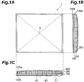
- a radiation image converting panel to be applied to such a radiation image recording and reproducing technique as this includes a support body and a radiation converting film provided on the support body.
- a photostimulable phosphor layer having a columnar crystal structure formed by vapor-phase growth (deposition) has been known.
- the photostimulable phosphor layer has a columnar crystal structure, since a photostimulable excitation light or photostimulable emission is effectively suppressed from diffusing in the horizontal direction (reaches the support body surface while repeating reflection at crack (columnar crystal) interfaces), this allows remarkably increasing the sharpness of an image by photostimulable emission.
- Japanese Patent Application Laid-Open No. H02-58000 has proposed a radiation image converting panel having a photostimulable phosphor layer for which formed by a vapor-phase deposition method on a support body are slender columnar crystals with a constant tilt with respect to a normal direction of the support body.
- Japanese Patent Application Laid-Open No. 2005-315786 has proposed a technique for preventing, by sealing a photostimulable phosphor layer formed on a support body with a moisture-proof protective film made of a base material having a surface roughness Ra of 20nm or less and a multilayered moisture-proof layer, deterioration of the photostimulable phosphor layer due to moisture and the like.
- the radiation converting film has a convex sectional shape
- a part of the radiation converting film having a maximum film thickness locates on a central area around the gravity center position whose radius equals 5% or less of a minimum distance from the gravity center position to an edge of the film forming region
- a part of the radiation converting film having a minimum film thickness locates on a peripheral area sandwiched by a circumference of a circle whose radius equals 80% of the minimum distance and the edge of the film forming region.
- the radiation converting film has a concave sectional shape
- a part of the radiation converting film having a minimum film thickness locates on a central area around the gravity center position whose radius equals 5% or less of a minimum distance from the gravity center position to an edge of the film forming region
- a part of the radiation converting film having a maximum film thickness locates on a peripheral area sandwiched by a circumference of a circle whose radius equals 80% of the minimum distance and the edge of the film forming region.
- the radiation converting film having such a concave sectional shape is effective when an attention imaging region exists in the periphery of the panel.
- the film thickness of the radiation converting film located on a peripheral area, which is sandwiched by the circumference of the circle defining the middle area and the edge of the film forming region monotonically decreases from the circumference of the circle defining the middle area toward the edge of the film forming region.
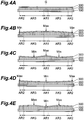
- Figs. 2A to 2C are views showing sectional structures of respective parts in a radiation converting film according to the present invention.
- Fig. 2A is a sectional view of a region A1 in Fig. 1C
- Fig. 2B is a sectional view of a region B 1 in Fig. 1C
- Fig. 2C is a sectional view of a region C1 in Fig. 1C .
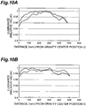
- 3C is a graph showing a relationship between the distance and a change in film thickness, wherein the minimum film thickness point, which is located on the central area AR1 and corresponds to the gravity center position G where the film thickness of the radiation converting film 200 is minimized, is assumed as the origin, a distance (>0) from the minimum film thickness point is assumed as the horizontal axis, and a film thickness (>0) of the radiation converting film 200 at a position corresponding to the distance from the minimum film thickness point is assumed as the longitudinal axis.
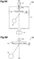
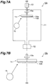
- Figs. 7A and 7B are views showing a configuration of a manufacturing apparatus 10c for forming, on the support body 100, a radiation converting film 200 with a film thickness increased from the vicinity of the center toward the periphery (a concave sectional shape), as a part of the manufacturing process of the radiation image converting panel 1 according to the present invention.
- the manufacturing apparatus 10c shown in Figs. 7A and 7B differs from the manufacturing apparatuses 10a and 10b shown in Figs. 5 , 6A, and 6B in terms of arrangement of the phosphor evaporation source 15 and inflow direction of a metal vapor.
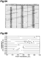
- Figs. 8A and 8B are a table and a graph showing relationships between the film thickness and luminance of the radiation converting films 200.
- Fig. 8A is a table showing numerical values when radiation converting film samples having various film thicknesses ( ⁇ m) were prepared and respective luminances were measured. In Fig. 8A , the luminances are shown as relative values (standardized values with the maximum value provided as 1).
- Fig. 8B is a graph plotting the relationships between the film thickness and luminance relative value shown in Fig. 8A .
Landscapes
- Physics & Mathematics (AREA)
- Health & Medical Sciences (AREA)
- Life Sciences & Earth Sciences (AREA)
- General Physics & Mathematics (AREA)
- High Energy & Nuclear Physics (AREA)
- Molecular Biology (AREA)
- Spectroscopy & Molecular Physics (AREA)
- Chemical & Material Sciences (AREA)
- Crystallography & Structural Chemistry (AREA)
- Conversion Of X-Rays Into Visible Images (AREA)
- Apparatus For Radiation Diagnosis (AREA)
Claims (10)
- Strahlungsbildwandler, mit:einem Halteteil (100) mit einer ersten Hauptoberfläche (100a) und einer zweiten Hauptoberfläche (100b), die der ersten Hauptoberfläche gegenüberliegt; undeiner Strahlungsumwandlungsschicht (200), die auf einem Schichtbildungsgebiet (R) vorgesehen ist, das in der ersten Hauptoberfläche des Halteteils vorhanden ist und zumindest eine Schwerpunktsposition (G) der ersten Hauptoberfläche enthält, wobei die Strahlungsumwandlungsschicht säulenartige Kristalle aufweist, die in Bezug auf eine Normalenrichtung der ersten Hauptoberfläche ausgerichtet oder unter einem bestimmten Winkel dazu geneigt sind,dadurch gekennzeichnet, dassin dem Schichtbildungsgebiet (R) der ersten Hauptoberfläche ein Teil der Strahlungsumwandlungsschicht, der eine maximale Schichtdicke hat, in einem zentralen Bereich (AR1) um die Schwerpunktsposition (G) herum angeordnet ist, dessen Radius 5% oder weniger eines minimalen Abstands (Wmin) von der Schwerpunktsposition zu einem Rand des Schichtbildungsgebiets beträgt, und wobei ein Teil der Strahlungsumwandlungsschicht, der eine minimale Schichtdicke hat, in einem mittleren Bereich (AR3) angeordnet ist, der von einem Umfang eines Kreises, dessen Radius gleich 80 % des minimalen Abstands beträgt, und einem Rand des zentralen Bereichs (AR1) eingeschlossen ist.
- Strahlungsbildwandler nach Anspruch 1, wobei die Schichtdicke der Strahlungsumwandlungsschicht (200), die an einem peripheren Bereich angeordnet ist, der von dem Umfang des Kreises, der den mittleren Bereich festlegt, und dem Rand des Schichtbildungsgebiets eingeschlossen ist, ausgehend von dem Umfang des Kreises, der den mittleren Bereich definiert, in Richtung zu dem Rand des Schichtbildungsgebiets (R) monoton zunimmt.
- Strahlungsbildwandler nach Anspruch 1, der ferner eine Schutzschicht (300) aufweist, die eine freiliegende Oberfläche der Strahlungsumwandlungsschicht (200) abdeckt, wobei eine Oberfläche ausgenommen ist, die von der Hauptoberfläche des Halteteils bedeckt ist.
- Strahlungsbildwandler, mit:einem Halteteil (100) mit einer ersten Hauptoberfläche (100a) und einer zweiten Hauptoberfläche (100b), die der ersten Hauptoberfläche gegenüberliegt; undeiner Strahlungsumwandlungsschicht (200), die auf einem Schichtbildungsgebiet (R) vorgesehen ist, das in der ersten Hauptoberfläche des Halteteils vorhanden ist und zumindest eine Schwerpunktsposition (G) der ersten Hauptoberfläche enthält, wobei die Strahlungsumwandlungsschicht säulenartige Kristalle aufweist, die in Bezug auf eine Normalenrichtung der ersten Hauptoberfläche ausgerichtet oder unter einem bestimmten Winkel dazu geneigt sind,dadurch gekennzeichnet, dassin dem Schichtbildungsgebiet der ersten Hauptoberfläche ein Teil der Strahlungsumwandlungsschicht, der eine minimale Schichtdicke hat, auf einem zentralen Bereich (AR1) um die Schwerpunktsposition herum angeordnet ist, dessen Radius gleich 5 % oder kleiner eines minimalen Abstands (Wmin) von der Schwerpunktsposition zu einem Rand des Schichtbildungsgebiets beträgt, und ein Teil der Strahlungsumwandlungsschicht, der eine maximale Schichtdicke hat, auf einem peripheren Bereich (AR2) liegt, der von einem Umfang eines Kreises, dessen Radius gleich 80 % des minimalen Abstands beträgt, und dem Rand des Schichtbildungsgebiets eingeschlossen ist.
- Strahlungsbildwandler nach Anspruch 4, wobei die Schichtdicke der Strahlungsumwandlungsschicht (200) von einem Punkt der minimalen Schichtdicke, der auf dem zentralen Bereich liegt und einer Position entspricht, an der die Schichtdicke der Strahlungsumwandlungsschicht minimal ist, zu einem Punkt maximaler Schichtdicke, der auf dem peripheren Bereich liegt und einer Position entspricht, an der die Schichtdicke der Strahlungsumwandlungsschicht maximal ist, monoton zunimmt.
- Strahlungsbildwandler nach Anspruch 5, wobei, wenn der Punkt der minimalen Schichtdicke als Ursprung, ein Abstand (>0) von dem Punkt der minimalen Schichtdicke als eine horizontale Achse und eine Schichtdicke (>0) der Strahlungsumwandlungsschicht (200) an einer Position, die dem Abstand zu dem Punkt der minimalen Schichtdicke entspricht, als eine Längsachse angenommen wird, dann eine gerade Linie, die den Punkt, der die minimale Schichtdicke angibt, mit dem Punkt verbindet, der die maximale Schichtdicke angibt, einen Gradienten von größer als 0 und kleiner als 0,002 hat.
- Strahlungsbildwandler nach Anspruch 4, der ferner eine Schutzschicht (300) aufweist, die eine freigelegte Oberfläche der Strahlungsumwandlungsschicht (200) abdeckt, wobei eine Oberfläche ausgenommen ist, die von der ersten Hauptoberfläche des Halteteils bedeckt ist.
- Strahlungsbildwandler, mit:einem Halteteil (100) mit einer ersten Hauptoberfläche (100a) und einer zweiten Hauptoberfläche (100b), die der ersten Hauptoberfläche gegenüberliegt; undeiner Strahlungsumwandlungsschicht (200), die auf einem Schichtbildungsgebiet (R) vorgesehen ist, das in der ersten Hauptoberfläche des Halteteils vorhanden ist und zumindest eine Schwerpunktsposition (G) der ersten Hauptoberfläche enthält, wobei die Strahlungsumwandlungsschicht säulenartige Kristalle aufweist, die in Bezug auf eine Normalenrichtung der ersten Hauptoberfläche ausgerichtet oder dazu unter einem vorbestimmten Winkel geneigt sind,dadurch gekennzeichnet, dassin dem Schichtbildungsgebiet der ersten Hauptoberfläche ein Teil der Strahlungsumwandlungsschicht, der eine minimale Schichtdicke hat, auf einem zentralen Bereich (AR1) um die Schwerpunktsposition herum liegt, dessen Radius gleich oder kleiner 5 % eines minimalen Abstands (Wmin) von der Schwerpunktsposition zu einem Rand des Schichtbildungsgebiets beträgt, und ein Teil der Strahlungsumwandlungsschicht, der eine maximale Schichtdicke hat, auf einem mittleren Bereich (AR3) liegt, der von einem Umfang eines Kreises, dessen Radius gleich 80 % des minimalen Abstands beträgt, und einem Umriss des zentralen Bereichs (AR1) eingeschlossen ist.
- Strahlungsbildwandler nach Anspruch 8, wobei die Schichtdicke der Strahlungsumwandlungsschicht (200), die auf einem peripheren Bereich liegt, der von dem Umfang des Kreises, der den mittleren Bereich definiert, und dem Rand des Schichtbildungsgebiets (R) eingeschlossen ist, von dem Umfang des Kreises, der den mittleren Bereich definiert, zu dem Rand des Schichtbildungsgebiets monoton abnimmt.
- Strahlungsbildwandler nach Anspruch 8, der ferner eine Schutzschicht (300) aufweist, die eine freigelegte Oberfläche der Strahlungsumwandlungsschicht abdeckt, wobei eine Oberfläche ausgenommen ist,
Applications Claiming Priority (1)
| Application Number | Priority Date | Filing Date | Title |
|---|---|---|---|
| JP2008110369A JP2009258054A (ja) | 2008-04-21 | 2008-04-21 | 放射線像変換パネル |
Publications (3)
| Publication Number | Publication Date |
|---|---|
| EP2159604A2 EP2159604A2 (de) | 2010-03-03 |
| EP2159604A3 EP2159604A3 (de) | 2016-12-07 |
| EP2159604B1 true EP2159604B1 (de) | 2019-04-17 |
Family
ID=41200330
Family Applications (1)
| Application Number | Title | Priority Date | Filing Date |
|---|---|---|---|
| EP08022501.4A Active EP2159604B1 (de) | 2008-04-21 | 2008-12-29 | Strahlungsbildwandler |
Country Status (3)
| Country | Link |
|---|---|
| US (1) | US7994490B2 (de) |
| EP (1) | EP2159604B1 (de) |
| JP (1) | JP2009258054A (de) |
Families Citing this family (1)
| Publication number | Priority date | Publication date | Assignee | Title |
|---|---|---|---|---|
| JP2015021752A (ja) | 2013-07-16 | 2015-02-02 | キヤノン株式会社 | 放射線撮像装置、その製造方法及び放射線検査装置 |
Family Cites Families (10)
| Publication number | Priority date | Publication date | Assignee | Title |
|---|---|---|---|---|
| US4947046A (en) * | 1988-05-27 | 1990-08-07 | Konica Corporation | Method for preparation of radiographic image conversion panel and radiographic image conversion panel thereby |
| DE69726252T2 (de) * | 1996-09-18 | 2004-08-26 | Kabushiki Kaisha Toshiba | Röntgenbildröhre und herstellungsverfahren für dieselbe |
| KR100514547B1 (ko) * | 1997-02-14 | 2005-12-14 | 하마마츠 포토닉스 가부시키가이샤 | 방사선검출소자및그제조방법 |
| JP4789372B2 (ja) | 2001-08-27 | 2011-10-12 | キヤノン株式会社 | 放射線検出装置、システム及びそれらに備えられるシンチレータパネル |
| JP4474877B2 (ja) | 2003-09-17 | 2010-06-09 | コニカミノルタエムジー株式会社 | 放射線画像変換パネル及び放射線画像変換パネルの製造方法 |
| WO2005038490A1 (en) * | 2003-10-22 | 2005-04-28 | Canon Kabushiki Kaisha | Radiation detection device, scintillator panel, method of making the same, making apparatus, and radiation image pick-up system |
| JP2005315786A (ja) | 2004-04-30 | 2005-11-10 | Fuji Photo Film Co Ltd | 放射線像変換パネル |
| JP4594188B2 (ja) * | 2004-08-10 | 2010-12-08 | キヤノン株式会社 | 放射線検出装置及び放射線検出システム |
| JP2006098239A (ja) * | 2004-09-29 | 2006-04-13 | Fuji Photo Film Co Ltd | 放射線像変換パネル |
| JP2006133152A (ja) * | 2004-11-09 | 2006-05-25 | Konica Minolta Medical & Graphic Inc | 放射線画像変換パネル |
-
2008
- 2008-04-21 JP JP2008110369A patent/JP2009258054A/ja active Pending
- 2008-12-29 EP EP08022501.4A patent/EP2159604B1/de active Active
-
2009
- 2009-01-08 US US12/350,500 patent/US7994490B2/en active Active
Also Published As
| Publication number | Publication date |
|---|---|
| EP2159604A3 (de) | 2016-12-07 |
| JP2009258054A (ja) | 2009-11-05 |
| US20090261254A1 (en) | 2009-10-22 |
| US7994490B2 (en) | 2011-08-09 |
| EP2159604A2 (de) | 2010-03-03 |
Similar Documents
| Publication | Publication Date | Title |
|---|---|---|
| EP2793052B1 (de) | Szintillatorarray sowie röntgendetektor und röntgenuntersuchungsvorrichtung mit dem szintillatorarray | |
| JP6241132B2 (ja) | シンチレータプレートおよび放射線検出パネル | |
| JP6488635B2 (ja) | シンチレータパネル及び放射線検出器 | |
| CN105572714B (zh) | 闪烁体面板及放射线检测器 | |
| JP5862302B2 (ja) | 放射線画像変換パネルとそれを用いた放射線画像検出器 | |
| JPWO2010150576A1 (ja) | シンチレータパネル、シンチレータパネルの製造方法、放射線画像検出器および放射線画像検出器の製造方法 | |
| US20120009375A1 (en) | Scintillator panel | |
| EP2343713B1 (de) | Strahlungsbildumwandlungstafel | |
| US9418768B2 (en) | Radiographic image conversion panel and radiographic image detector | |
| EP2159604B1 (de) | Strahlungsbildwandler | |
| US20080006780A1 (en) | Radiation image conversion panel and process for producing the same | |
| EP2439749A1 (de) | Verfahren zur herstellung einer szintillatorplatte, szintillatorplatte und röntgenbilddetektor | |
| JP3130633B2 (ja) | 放射線画像変換パネルの製造方法 | |
| EP2112667B1 (de) | Strahlungsbildumwandlungstafel | |
| EP2112668B1 (de) | Strahlungsbildumwandlungstafel | |
| JP6436793B2 (ja) | シンチレータパネル、放射線検出器及びそれらの製造方法。 | |
| EP2998964A1 (de) | Umwandlungstafel für strahlungsbilder | |
| JP2005222023A (ja) | 放射線画像読取方法及び放射線画像読取装置並びに輝尽性蛍光体プレート | |
| US20070096041A1 (en) | Stimulable phosphor panel and method of producing stimulable phosphor panel | |
| JP2010060414A (ja) | シンチレータプレート | |
| WO2007060814A1 (ja) | 放射線用シンチレータプレート | |
| US20020179869A1 (en) | Radiation image read-out method and apparatus, and stimulable phosphor sheet | |
| US20060249691A1 (en) | Radiation image conversion panel | |
| Nakazawa et al. | X-ray section topographs of a cube-shaped diamond | |
| JP2004059976A (ja) | 基板支持装置 |
Legal Events
| Date | Code | Title | Description |
|---|---|---|---|
| PUAI | Public reference made under article 153(3) epc to a published international application that has entered the european phase |
Free format text: ORIGINAL CODE: 0009012 |
|
| AK | Designated contracting states |
Kind code of ref document: A2 Designated state(s): AT BE BG CH CY CZ DE DK EE ES FI FR GB GR HR HU IE IS IT LI LT LU LV MC MT NL NO PL PT RO SE SI SK TR |
|
| AX | Request for extension of the european patent |
Extension state: AL BA MK RS |
|
| PUAL | Search report despatched |
Free format text: ORIGINAL CODE: 0009013 |
|
| AK | Designated contracting states |
Kind code of ref document: A3 Designated state(s): AT BE BG CH CY CZ DE DK EE ES FI FR GB GR HR HU IE IS IT LI LT LU LV MC MT NL NO PL PT RO SE SI SK TR |
|
| AX | Request for extension of the european patent |
Extension state: AL BA MK RS |
|
| RIC1 | Information provided on ipc code assigned before grant |
Ipc: G01T 1/202 20060101ALI20161031BHEP Ipc: G01T 1/29 20060101ALI20161031BHEP Ipc: G01T 1/20 20060101AFI20161031BHEP |
|
| STAA | Information on the status of an ep patent application or granted ep patent |
Free format text: STATUS: REQUEST FOR EXAMINATION WAS MADE |
|
| 17P | Request for examination filed |
Effective date: 20170116 |
|
| RBV | Designated contracting states (corrected) |
Designated state(s): AT BE BG CH CY CZ DE DK EE ES FI FR GB GR HR HU IE IS IT LI LT LU LV MC MT NL NO PL PT RO SE SI SK TR |
|
| AKX | Designation fees paid |
Designated state(s): AT BE BG CH CY CZ DE DK EE ES FI FR GB GR HR HU IE IS IT LI LT LU LV MC MT NL NO PL PT RO SE SI SK TR |
|
| GRAP | Despatch of communication of intention to grant a patent |
Free format text: ORIGINAL CODE: EPIDOSNIGR1 |
|
| STAA | Information on the status of an ep patent application or granted ep patent |
Free format text: STATUS: GRANT OF PATENT IS INTENDED |
|
| INTG | Intention to grant announced |
Effective date: 20181029 |
|
| GRAS | Grant fee paid |
Free format text: ORIGINAL CODE: EPIDOSNIGR3 |
|
| GRAA | (expected) grant |
Free format text: ORIGINAL CODE: 0009210 |
|
| STAA | Information on the status of an ep patent application or granted ep patent |
Free format text: STATUS: THE PATENT HAS BEEN GRANTED |
|
| AK | Designated contracting states |
Kind code of ref document: B1 Designated state(s): AT BE BG CH CY CZ DE DK EE ES FI FR GB GR HR HU IE IS IT LI LT LU LV MC MT NL NO PL PT RO SE SI SK TR |
|
| REG | Reference to a national code |
Ref country code: GB Ref legal event code: FG4D |
|
| REG | Reference to a national code |
Ref country code: CH Ref legal event code: EP |
|
| REG | Reference to a national code |
Ref country code: DE Ref legal event code: R096 Ref document number: 602008059752 Country of ref document: DE |
|
| REG | Reference to a national code |
Ref country code: AT Ref legal event code: REF Ref document number: 1122188 Country of ref document: AT Kind code of ref document: T Effective date: 20190515 Ref country code: IE Ref legal event code: FG4D |
|
| REG | Reference to a national code |
Ref country code: SE Ref legal event code: TRGR |
|
| REG | Reference to a national code |
Ref country code: NL Ref legal event code: MP Effective date: 20190417 |
|
| REG | Reference to a national code |
Ref country code: LT Ref legal event code: MG4D |
|
| PG25 | Lapsed in a contracting state [announced via postgrant information from national office to epo] |
Ref country code: NL Free format text: LAPSE BECAUSE OF FAILURE TO SUBMIT A TRANSLATION OF THE DESCRIPTION OR TO PAY THE FEE WITHIN THE PRESCRIBED TIME-LIMIT Effective date: 20190417 |
|
| PG25 | Lapsed in a contracting state [announced via postgrant information from national office to epo] |
Ref country code: LT Free format text: LAPSE BECAUSE OF FAILURE TO SUBMIT A TRANSLATION OF THE DESCRIPTION OR TO PAY THE FEE WITHIN THE PRESCRIBED TIME-LIMIT Effective date: 20190417 Ref country code: FI Free format text: LAPSE BECAUSE OF FAILURE TO SUBMIT A TRANSLATION OF THE DESCRIPTION OR TO PAY THE FEE WITHIN THE PRESCRIBED TIME-LIMIT Effective date: 20190417 Ref country code: ES Free format text: LAPSE BECAUSE OF FAILURE TO SUBMIT A TRANSLATION OF THE DESCRIPTION OR TO PAY THE FEE WITHIN THE PRESCRIBED TIME-LIMIT Effective date: 20190417 Ref country code: HR Free format text: LAPSE BECAUSE OF FAILURE TO SUBMIT A TRANSLATION OF THE DESCRIPTION OR TO PAY THE FEE WITHIN THE PRESCRIBED TIME-LIMIT Effective date: 20190417 Ref country code: NO Free format text: LAPSE BECAUSE OF FAILURE TO SUBMIT A TRANSLATION OF THE DESCRIPTION OR TO PAY THE FEE WITHIN THE PRESCRIBED TIME-LIMIT Effective date: 20190717 Ref country code: PT Free format text: LAPSE BECAUSE OF FAILURE TO SUBMIT A TRANSLATION OF THE DESCRIPTION OR TO PAY THE FEE WITHIN THE PRESCRIBED TIME-LIMIT Effective date: 20190817 |
|
| PG25 | Lapsed in a contracting state [announced via postgrant information from national office to epo] |
Ref country code: GR Free format text: LAPSE BECAUSE OF FAILURE TO SUBMIT A TRANSLATION OF THE DESCRIPTION OR TO PAY THE FEE WITHIN THE PRESCRIBED TIME-LIMIT Effective date: 20190718 Ref country code: PL Free format text: LAPSE BECAUSE OF FAILURE TO SUBMIT A TRANSLATION OF THE DESCRIPTION OR TO PAY THE FEE WITHIN THE PRESCRIBED TIME-LIMIT Effective date: 20190417 Ref country code: LV Free format text: LAPSE BECAUSE OF FAILURE TO SUBMIT A TRANSLATION OF THE DESCRIPTION OR TO PAY THE FEE WITHIN THE PRESCRIBED TIME-LIMIT Effective date: 20190417 Ref country code: BG Free format text: LAPSE BECAUSE OF FAILURE TO SUBMIT A TRANSLATION OF THE DESCRIPTION OR TO PAY THE FEE WITHIN THE PRESCRIBED TIME-LIMIT Effective date: 20190717 |
|
| REG | Reference to a national code |
Ref country code: AT Ref legal event code: MK05 Ref document number: 1122188 Country of ref document: AT Kind code of ref document: T Effective date: 20190417 |
|
| PG25 | Lapsed in a contracting state [announced via postgrant information from national office to epo] |
Ref country code: IS Free format text: LAPSE BECAUSE OF FAILURE TO SUBMIT A TRANSLATION OF THE DESCRIPTION OR TO PAY THE FEE WITHIN THE PRESCRIBED TIME-LIMIT Effective date: 20190817 |
|
| REG | Reference to a national code |
Ref country code: DE Ref legal event code: R097 Ref document number: 602008059752 Country of ref document: DE |
|
| PG25 | Lapsed in a contracting state [announced via postgrant information from national office to epo] |
Ref country code: SK Free format text: LAPSE BECAUSE OF FAILURE TO SUBMIT A TRANSLATION OF THE DESCRIPTION OR TO PAY THE FEE WITHIN THE PRESCRIBED TIME-LIMIT Effective date: 20190417 Ref country code: EE Free format text: LAPSE BECAUSE OF FAILURE TO SUBMIT A TRANSLATION OF THE DESCRIPTION OR TO PAY THE FEE WITHIN THE PRESCRIBED TIME-LIMIT Effective date: 20190417 Ref country code: CZ Free format text: LAPSE BECAUSE OF FAILURE TO SUBMIT A TRANSLATION OF THE DESCRIPTION OR TO PAY THE FEE WITHIN THE PRESCRIBED TIME-LIMIT Effective date: 20190417 Ref country code: RO Free format text: LAPSE BECAUSE OF FAILURE TO SUBMIT A TRANSLATION OF THE DESCRIPTION OR TO PAY THE FEE WITHIN THE PRESCRIBED TIME-LIMIT Effective date: 20190417 Ref country code: AT Free format text: LAPSE BECAUSE OF FAILURE TO SUBMIT A TRANSLATION OF THE DESCRIPTION OR TO PAY THE FEE WITHIN THE PRESCRIBED TIME-LIMIT Effective date: 20190417 Ref country code: DK Free format text: LAPSE BECAUSE OF FAILURE TO SUBMIT A TRANSLATION OF THE DESCRIPTION OR TO PAY THE FEE WITHIN THE PRESCRIBED TIME-LIMIT Effective date: 20190417 |
|
| PLBE | No opposition filed within time limit |
Free format text: ORIGINAL CODE: 0009261 |
|
| STAA | Information on the status of an ep patent application or granted ep patent |
Free format text: STATUS: NO OPPOSITION FILED WITHIN TIME LIMIT |
|
| PG25 | Lapsed in a contracting state [announced via postgrant information from national office to epo] |
Ref country code: IT Free format text: LAPSE BECAUSE OF FAILURE TO SUBMIT A TRANSLATION OF THE DESCRIPTION OR TO PAY THE FEE WITHIN THE PRESCRIBED TIME-LIMIT Effective date: 20190417 |
|
| 26N | No opposition filed |
Effective date: 20200120 |
|
| PG25 | Lapsed in a contracting state [announced via postgrant information from national office to epo] |
Ref country code: TR Free format text: LAPSE BECAUSE OF FAILURE TO SUBMIT A TRANSLATION OF THE DESCRIPTION OR TO PAY THE FEE WITHIN THE PRESCRIBED TIME-LIMIT Effective date: 20190417 |
|
| PG25 | Lapsed in a contracting state [announced via postgrant information from national office to epo] |
Ref country code: SI Free format text: LAPSE BECAUSE OF FAILURE TO SUBMIT A TRANSLATION OF THE DESCRIPTION OR TO PAY THE FEE WITHIN THE PRESCRIBED TIME-LIMIT Effective date: 20190417 |
|
| REG | Reference to a national code |
Ref country code: CH Ref legal event code: PL |
|
| REG | Reference to a national code |
Ref country code: BE Ref legal event code: MM Effective date: 20191231 |
|
| PG25 | Lapsed in a contracting state [announced via postgrant information from national office to epo] |
Ref country code: MC Free format text: LAPSE BECAUSE OF FAILURE TO SUBMIT A TRANSLATION OF THE DESCRIPTION OR TO PAY THE FEE WITHIN THE PRESCRIBED TIME-LIMIT Effective date: 20190417 |
|
| PG25 | Lapsed in a contracting state [announced via postgrant information from national office to epo] |
Ref country code: IE Free format text: LAPSE BECAUSE OF NON-PAYMENT OF DUE FEES Effective date: 20191229 Ref country code: LU Free format text: LAPSE BECAUSE OF NON-PAYMENT OF DUE FEES Effective date: 20191229 |
|
| PG25 | Lapsed in a contracting state [announced via postgrant information from national office to epo] |
Ref country code: CH Free format text: LAPSE BECAUSE OF NON-PAYMENT OF DUE FEES Effective date: 20191231 Ref country code: LI Free format text: LAPSE BECAUSE OF NON-PAYMENT OF DUE FEES Effective date: 20191231 Ref country code: BE Free format text: LAPSE BECAUSE OF NON-PAYMENT OF DUE FEES Effective date: 20191231 |
|
| PG25 | Lapsed in a contracting state [announced via postgrant information from national office to epo] |
Ref country code: CY Free format text: LAPSE BECAUSE OF FAILURE TO SUBMIT A TRANSLATION OF THE DESCRIPTION OR TO PAY THE FEE WITHIN THE PRESCRIBED TIME-LIMIT Effective date: 20190417 |
|
| PG25 | Lapsed in a contracting state [announced via postgrant information from national office to epo] |
Ref country code: HU Free format text: LAPSE BECAUSE OF FAILURE TO SUBMIT A TRANSLATION OF THE DESCRIPTION OR TO PAY THE FEE WITHIN THE PRESCRIBED TIME-LIMIT; INVALID AB INITIO Effective date: 20081229 Ref country code: MT Free format text: LAPSE BECAUSE OF FAILURE TO SUBMIT A TRANSLATION OF THE DESCRIPTION OR TO PAY THE FEE WITHIN THE PRESCRIBED TIME-LIMIT Effective date: 20190417 |
|
| P01 | Opt-out of the competence of the unified patent court (upc) registered |
Effective date: 20230509 |
|
| PGFP | Annual fee paid to national office [announced via postgrant information from national office to epo] |
Ref country code: DE Payment date: 20251104 Year of fee payment: 18 |
|
| PGFP | Annual fee paid to national office [announced via postgrant information from national office to epo] |
Ref country code: GB Payment date: 20251114 Year of fee payment: 18 |
|
| PGFP | Annual fee paid to national office [announced via postgrant information from national office to epo] |
Ref country code: FR Payment date: 20251110 Year of fee payment: 18 |
|
| PGFP | Annual fee paid to national office [announced via postgrant information from national office to epo] |
Ref country code: SE Payment date: 20251112 Year of fee payment: 18 |