EP2157689B1 - Motor control device - Google Patents
Motor control device Download PDFInfo
- Publication number
- EP2157689B1 EP2157689B1 EP08851581.2A EP08851581A EP2157689B1 EP 2157689 B1 EP2157689 B1 EP 2157689B1 EP 08851581 A EP08851581 A EP 08851581A EP 2157689 B1 EP2157689 B1 EP 2157689B1
- Authority
- EP
- European Patent Office
- Prior art keywords
- voltage circuit
- circuit
- voltage
- low
- circuit area
- Prior art date
- Legal status (The legal status is an assumption and is not a legal conclusion. Google has not performed a legal analysis and makes no representation as to the accuracy of the status listed.)
- Active
Links
- 238000009413 insulation Methods 0.000 claims description 135
- 239000000758 substrate Substances 0.000 claims description 45
- 238000001514 detection method Methods 0.000 claims description 37
- 239000000306 component Substances 0.000 description 10
- 238000010586 diagram Methods 0.000 description 7
- 239000002184 metal Substances 0.000 description 6
- 230000005856 abnormality Effects 0.000 description 4
- 238000010438 heat treatment Methods 0.000 description 4
- 230000002452 interceptive effect Effects 0.000 description 3
- 238000013021 overheating Methods 0.000 description 3
- 230000005540 biological transmission Effects 0.000 description 2
- 230000015572 biosynthetic process Effects 0.000 description 2
- 239000000919 ceramic Substances 0.000 description 2
- 230000007423 decrease Effects 0.000 description 2
- 230000008054 signal transmission Effects 0.000 description 2
- 230000002159 abnormal effect Effects 0.000 description 1
- 239000008358 core component Substances 0.000 description 1
- 230000005669 field effect Effects 0.000 description 1
- 238000009499 grossing Methods 0.000 description 1
- 230000005855 radiation Effects 0.000 description 1
- 229910000679 solder Inorganic materials 0.000 description 1
- 230000000087 stabilizing effect Effects 0.000 description 1
- 230000009466 transformation Effects 0.000 description 1
- 238000003466 welding Methods 0.000 description 1
Images


Classifications
-
- H—ELECTRICITY
- H02—GENERATION; CONVERSION OR DISTRIBUTION OF ELECTRIC POWER
- H02M—APPARATUS FOR CONVERSION BETWEEN AC AND AC, BETWEEN AC AND DC, OR BETWEEN DC AND DC, AND FOR USE WITH MAINS OR SIMILAR POWER SUPPLY SYSTEMS; CONVERSION OF DC OR AC INPUT POWER INTO SURGE OUTPUT POWER; CONTROL OR REGULATION THEREOF
- H02M7/00—Conversion of ac power input into dc power output; Conversion of dc power input into ac power output
- H02M7/42—Conversion of dc power input into ac power output without possibility of reversal
- H02M7/44—Conversion of dc power input into ac power output without possibility of reversal by static converters
- H02M7/48—Conversion of dc power input into ac power output without possibility of reversal by static converters using discharge tubes with control electrode or semiconductor devices with control electrode
-
- H—ELECTRICITY
- H03—ELECTRONIC CIRCUITRY
- H03K—PULSE TECHNIQUE
- H03K17/00—Electronic switching or gating, i.e. not by contact-making and –breaking
- H03K17/08—Modifications for protecting switching circuit against overcurrent or overvoltage
- H03K17/082—Modifications for protecting switching circuit against overcurrent or overvoltage by feedback from the output to the control circuit
- H03K17/0828—Modifications for protecting switching circuit against overcurrent or overvoltage by feedback from the output to the control circuit in composite switches
-
- B—PERFORMING OPERATIONS; TRANSPORTING
- B60—VEHICLES IN GENERAL
- B60L—PROPULSION OF ELECTRICALLY-PROPELLED VEHICLES; SUPPLYING ELECTRIC POWER FOR AUXILIARY EQUIPMENT OF ELECTRICALLY-PROPELLED VEHICLES; ELECTRODYNAMIC BRAKE SYSTEMS FOR VEHICLES IN GENERAL; MAGNETIC SUSPENSION OR LEVITATION FOR VEHICLES; MONITORING OPERATING VARIABLES OF ELECTRICALLY-PROPELLED VEHICLES; ELECTRIC SAFETY DEVICES FOR ELECTRICALLY-PROPELLED VEHICLES
- B60L58/00—Methods or circuit arrangements for monitoring or controlling batteries or fuel cells, specially adapted for electric vehicles
- B60L58/10—Methods or circuit arrangements for monitoring or controlling batteries or fuel cells, specially adapted for electric vehicles for monitoring or controlling batteries
- B60L58/18—Methods or circuit arrangements for monitoring or controlling batteries or fuel cells, specially adapted for electric vehicles for monitoring or controlling batteries of two or more battery modules
- B60L58/20—Methods or circuit arrangements for monitoring or controlling batteries or fuel cells, specially adapted for electric vehicles for monitoring or controlling batteries of two or more battery modules having different nominal voltages
-
- H—ELECTRICITY
- H02—GENERATION; CONVERSION OR DISTRIBUTION OF ELECTRIC POWER
- H02M—APPARATUS FOR CONVERSION BETWEEN AC AND AC, BETWEEN AC AND DC, OR BETWEEN DC AND DC, AND FOR USE WITH MAINS OR SIMILAR POWER SUPPLY SYSTEMS; CONVERSION OF DC OR AC INPUT POWER INTO SURGE OUTPUT POWER; CONTROL OR REGULATION THEREOF
- H02M1/00—Details of apparatus for conversion
- H02M1/08—Circuits specially adapted for the generation of control voltages for semiconductor devices incorporated in static converters
-
- H—ELECTRICITY
- H02—GENERATION; CONVERSION OR DISTRIBUTION OF ELECTRIC POWER
- H02M—APPARATUS FOR CONVERSION BETWEEN AC AND AC, BETWEEN AC AND DC, OR BETWEEN DC AND DC, AND FOR USE WITH MAINS OR SIMILAR POWER SUPPLY SYSTEMS; CONVERSION OF DC OR AC INPUT POWER INTO SURGE OUTPUT POWER; CONTROL OR REGULATION THEREOF
- H02M3/00—Conversion of dc power input into dc power output
- H02M3/22—Conversion of dc power input into dc power output with intermediate conversion into ac
- H02M3/24—Conversion of dc power input into dc power output with intermediate conversion into ac by static converters
- H02M3/28—Conversion of dc power input into dc power output with intermediate conversion into ac by static converters using discharge tubes with control electrode or semiconductor devices with control electrode to produce the intermediate ac
- H02M3/325—Conversion of dc power input into dc power output with intermediate conversion into ac by static converters using discharge tubes with control electrode or semiconductor devices with control electrode to produce the intermediate ac using devices of a triode or a transistor type requiring continuous application of a control signal
- H02M3/335—Conversion of dc power input into dc power output with intermediate conversion into ac by static converters using discharge tubes with control electrode or semiconductor devices with control electrode to produce the intermediate ac using devices of a triode or a transistor type requiring continuous application of a control signal using semiconductor devices only
- H02M3/337—Conversion of dc power input into dc power output with intermediate conversion into ac by static converters using discharge tubes with control electrode or semiconductor devices with control electrode to produce the intermediate ac using devices of a triode or a transistor type requiring continuous application of a control signal using semiconductor devices only in push-pull configuration
-
- H—ELECTRICITY
- H02—GENERATION; CONVERSION OR DISTRIBUTION OF ELECTRIC POWER
- H02M—APPARATUS FOR CONVERSION BETWEEN AC AND AC, BETWEEN AC AND DC, OR BETWEEN DC AND DC, AND FOR USE WITH MAINS OR SIMILAR POWER SUPPLY SYSTEMS; CONVERSION OF DC OR AC INPUT POWER INTO SURGE OUTPUT POWER; CONTROL OR REGULATION THEREOF
- H02M7/00—Conversion of ac power input into dc power output; Conversion of dc power input into ac power output
- H02M7/003—Constructional details, e.g. physical layout, assembly, wiring or busbar connections
-
- H—ELECTRICITY
- H02—GENERATION; CONVERSION OR DISTRIBUTION OF ELECTRIC POWER
- H02M—APPARATUS FOR CONVERSION BETWEEN AC AND AC, BETWEEN AC AND DC, OR BETWEEN DC AND DC, AND FOR USE WITH MAINS OR SIMILAR POWER SUPPLY SYSTEMS; CONVERSION OF DC OR AC INPUT POWER INTO SURGE OUTPUT POWER; CONTROL OR REGULATION THEREOF
- H02M7/00—Conversion of ac power input into dc power output; Conversion of dc power input into ac power output
- H02M7/42—Conversion of dc power input into ac power output without possibility of reversal
- H02M7/44—Conversion of dc power input into ac power output without possibility of reversal by static converters
- H02M7/48—Conversion of dc power input into ac power output without possibility of reversal by static converters using discharge tubes with control electrode or semiconductor devices with control electrode
- H02M7/53—Conversion of dc power input into ac power output without possibility of reversal by static converters using discharge tubes with control electrode or semiconductor devices with control electrode using devices of a triode or transistor type requiring continuous application of a control signal
- H02M7/537—Conversion of dc power input into ac power output without possibility of reversal by static converters using discharge tubes with control electrode or semiconductor devices with control electrode using devices of a triode or transistor type requiring continuous application of a control signal using semiconductor devices only, e.g. single switched pulse inverters
- H02M7/5387—Conversion of dc power input into ac power output without possibility of reversal by static converters using discharge tubes with control electrode or semiconductor devices with control electrode using devices of a triode or transistor type requiring continuous application of a control signal using semiconductor devices only, e.g. single switched pulse inverters in a bridge configuration
-
- H—ELECTRICITY
- H02—GENERATION; CONVERSION OR DISTRIBUTION OF ELECTRIC POWER
- H02P—CONTROL OR REGULATION OF ELECTRIC MOTORS, ELECTRIC GENERATORS OR DYNAMO-ELECTRIC CONVERTERS; CONTROLLING TRANSFORMERS, REACTORS OR CHOKE COILS
- H02P27/00—Arrangements or methods for the control of AC motors characterised by the kind of supply voltage
- H02P27/04—Arrangements or methods for the control of AC motors characterised by the kind of supply voltage using variable-frequency supply voltage, e.g. inverter or converter supply voltage
- H02P27/06—Arrangements or methods for the control of AC motors characterised by the kind of supply voltage using variable-frequency supply voltage, e.g. inverter or converter supply voltage using dc to ac converters or inverters
-
- H—ELECTRICITY
- H02—GENERATION; CONVERSION OR DISTRIBUTION OF ELECTRIC POWER
- H02M—APPARATUS FOR CONVERSION BETWEEN AC AND AC, BETWEEN AC AND DC, OR BETWEEN DC AND DC, AND FOR USE WITH MAINS OR SIMILAR POWER SUPPLY SYSTEMS; CONVERSION OF DC OR AC INPUT POWER INTO SURGE OUTPUT POWER; CONTROL OR REGULATION THEREOF
- H02M1/00—Details of apparatus for conversion
- H02M1/0003—Details of control, feedback or regulation circuits
- H02M1/0006—Arrangements for supplying an adequate voltage to the control circuit of converters
-
- H—ELECTRICITY
- H03—ELECTRONIC CIRCUITRY
- H03K—PULSE TECHNIQUE
- H03K17/00—Electronic switching or gating, i.e. not by contact-making and –breaking
- H03K17/08—Modifications for protecting switching circuit against overcurrent or overvoltage
- H03K2017/0806—Modifications for protecting switching circuit against overcurrent or overvoltage against excessive temperature
-
- H—ELECTRICITY
- H05—ELECTRIC TECHNIQUES NOT OTHERWISE PROVIDED FOR
- H05K—PRINTED CIRCUITS; CASINGS OR CONSTRUCTIONAL DETAILS OF ELECTRIC APPARATUS; MANUFACTURE OF ASSEMBLAGES OF ELECTRICAL COMPONENTS
- H05K1/00—Printed circuits
- H05K1/02—Details
- H05K1/0213—Electrical arrangements not otherwise provided for
- H05K1/0254—High voltage adaptations; Electrical insulation details; Overvoltage or electrostatic discharge protection ; Arrangements for regulating voltages or for using plural voltages
- H05K1/0262—Arrangements for regulating voltages or for using plural voltages
-
- Y—GENERAL TAGGING OF NEW TECHNOLOGICAL DEVELOPMENTS; GENERAL TAGGING OF CROSS-SECTIONAL TECHNOLOGIES SPANNING OVER SEVERAL SECTIONS OF THE IPC; TECHNICAL SUBJECTS COVERED BY FORMER USPC CROSS-REFERENCE ART COLLECTIONS [XRACs] AND DIGESTS
- Y02—TECHNOLOGIES OR APPLICATIONS FOR MITIGATION OR ADAPTATION AGAINST CLIMATE CHANGE
- Y02T—CLIMATE CHANGE MITIGATION TECHNOLOGIES RELATED TO TRANSPORTATION
- Y02T10/00—Road transport of goods or passengers
- Y02T10/60—Other road transportation technologies with climate change mitigation effect
- Y02T10/70—Energy storage systems for electromobility, e.g. batteries
Landscapes
- Engineering & Computer Science (AREA)
- Power Engineering (AREA)
- Life Sciences & Earth Sciences (AREA)
- Sustainable Development (AREA)
- Sustainable Energy (AREA)
- Transportation (AREA)
- Mechanical Engineering (AREA)
- Inverter Devices (AREA)
- Control Of Ac Motors In General (AREA)
Description
- The present invention relates to a motor control device for controlling an AC motor.
- A high-output motor used for powering an electric vehicle, hybrid vehicle, or the like is driven at a high voltage. Since a DC battery is mounted as a power source mounted in such a vehicle, the current is converted into a three-phase AC current by an inverter circuit that uses a switching element such as an insulated gate bipolar transistor (IGBT). A signal for driving the inverter circuit, e.g. a drive signal for driving a gate of the IGBT, is generated in a control circuit of a low-voltage circuit that is insulated from a high-voltage circuit driving the motor, and operates at a much lower voltage than that of the high-voltage circuit. Accordingly, a motor control device driving the motor is provided with an IGBT drive circuit for driving the IGBT of the inverter circuit based on the drive signal. In other words, as illustrated in
FIG. 6 , the motor control device is structured having amotor control circuit 300 that operates within the low-voltage circuit; anIGBT drive circuit 200 that operates within the high-voltage circuit and drives the IGBT based on a drive signal generated by themotor control circuit 300; and aninverter circuit 100 that is structured from a plurality of IGBTs. - The
inverter circuit 100 generating a three-phase AC current is structured from six IGBTs. The respective IGBTs operate independently, and gate drive circuits for driving the gates of the IGBTs are thus provided mutually independent in theIGBT drive circuit 200. Since the IGBTs handle a high voltage, the gate drive circuits driving the IGBTs must be arranged having a suitable insulation distance. -
Patent Document 1 discloses art for a voltage control device that is provided with a plurality of gate drive circuits for driving a plurality of IGBTs. According toPatent Document 1, a control circuit and the gate drive circuit are disposed at least separated by an insulation distance that corresponds to a distance between an input pin and an output pin of a transformer. The gate drive circuits are also disposed separated by a predetermined insulation distance. - The electromagnetic compatibility and size of a motor control circuit can be improved by using power supplies for the driving stages formed with individual transformers and transistors in push-pull configuration. Examples are shown in documents
JPH11178356 JP2006109686 JP-A-2006-280148 paragraphs FIG. 1 , etc.) - The voltage control device disclosed in
Patent Document 1 has three gate drive circuits; however, six gate drive circuits must be provided in an inverter circuit generating a three-phase AC current. Simply aligning two of the voltage control devices according toPatent Document 1 enlarges an insulation area where components cannot be mounted, and unnecessarily increases the surface area of the substrate. - The present invention was conceived in light of the foregoing issue, and it is an object of the present invention to provide a control device for an AC motor that is capable of securing insulation between a low-voltage circuit and a high-voltage circuit, while also achieving a compact size.
- In order to achieve the above object, a motor control device according to the present, as set forth in
claim 1, has a characteristic structure including a drive circuit that is respectively provided on arms of an inverter circuit supplying current to an AC motor, and that drives a switching element included on the arms; and a power source control circuit that performs a control of a power supply circuit for supplying power to the drive circuit. The characteristic structure of the motor control device further includes: a low-voltage circuit area that includes the power source control circuit; a high-voltage circuit area that includes one drive circuit, wherein a plurality of the high-voltage circuit areas is disposed aligned on both sides of the low-voltage circuit area such that the low-voltage circuit area is provided therebetween and also disposed with a predetermined distance provided between the high-voltage circuit area and the low-voltage circuit area; and a transformer that serves as the power supply circuit and respectively joins the low-voltage circuit area and the high-voltage circuit areas in an insulated state. - According to this characteristic structure, the drive circuits are disposed aligned on both sides of the low-voltage circuit area such that the low-voltage circuit area having the power source control circuit is provided therebetween. Power is supplied to the drive circuit via the transformer, which respectively joins the low-voltage circuit area and the high-voltage circuit areas in an insulated state. The power supplied to the drive circuit has a high voltage, and the high voltage appears on the high voltage circuit area side of the transformer. Therefore, high-voltage wiring is not drawn out over a long distance within a substrate. As a consequence, it is possible to decrease the surface area of an insulation area, where no parts for securing insulation distance can be mounted, and the substrate can be effectively utilized. The transformers connected to the drive circuits can also be controlled by a shared power source control circuit formed in the low-voltage circuit area. There is thus no need to individually provide power source control circuits with respect to the transformers, making it possible to simplify the power source control circuit. It is thus possible to keep the surface area of the substrate down and achieve a more compact motor control device. By providing the transformer, which is a heat-generating part, in a dispersed manner with respect to the drive circuits, the concentration of heat is less prone to occur and is an easy countermeasure against heat radiation.
- The motor control device according to the present invention is characterized in that the drive circuit is disposed with a predetermined insulation distance provided between adjacent drive circuits.
- The switching element included on the arms of the inverter circuit is driven so as to switch at a timing that differs for each arm. The drive circuit drives the switching element by controlling a difference in potential between two terminals, i.e., a gate terminal and a base terminal, or a source terminal and an emitter terminal, of the switching element. Since a DC power source voltage of the inverter circuit is extremely high, the difference in potential between two terminals for driving the switching element is a higher voltage than the power source voltage in the low-voltage circuit area. Also, when the switching element is in an on state, a voltage of the drive signal changes depending on the DC power source voltage connected with the switching element. As mentioned above, due to the different timings at which the drive signal is output from adjacent drive circuits, the change in the voltage of the drive signal also varies, thus generating a large difference in potential between the drive signals output from adjacent drive circuits. As a consequence, insulation must be secured between adjacent drive circuits, and adjacent drive circuits are preferably disposed with a predetermined insulation distance provided as in the present structure.
- The drive circuit of the motor control device according to the present invention is characterized in that a plurality of upper-level drive circuits that drive the switching element on a plurality of upper-level arms connected with a positive side of a DC power source of the inverter circuit is arranged aligned on a side of the low-voltage circuit area, and a plurality of lower-level drive circuits that drive the switching element on a plurality of lower-level arms connected with a negative side of the DC power source of the inverter circuit is arranged aligned on another side of the low-voltage circuit area.
- In the inverter circuit, the switching element on the upper-level arm is connected with a positive side of the DC power source, and the switching element on the lower-level arm is connected with a negative side of the DC power source. Arranging the switching element on the upper-level arm and the switching element on the lower-level arm in respective rows thus facilitates connection with a positive-side voltage and a negative-side voltage. Accordingly, arranging the drive circuit driving the switching element according to the respective rows of the upper-level drive circuits and the lower-level drive circuits also helps enable efficient wiring. As a consequence, a more compact motor control device can be achieved.
- The motor control device according to the present invention is characterized in that an insulation distance provided between adjacent upper-level drive circuits is set longer than an insulation distance provided between adjacent lower-level drive circuits.
- For the switching element on the upper-level arm connected with the positive side of the DC power source voltage of the inverter circuit, a potential of the emitter terminal or source terminal when in an on state increases to roughly a positive-side potential. Since the switching element on the lower-level arm is connected with the low-voltage negative side (commonly a ground), the emitter terminal or the source terminal when in an on state is a negative-side potential. The drive circuit in general drives the switching element by controlling a difference in potential between two terminals, i.e., the gate terminal and the base terminal, or the source terminal and the emitter terminal, of the switching element. Therefore, the potential of the upper-level drive circuit connected with the switching element of the upper-level arm increases to near the positive-side power source voltage of the inverter circuit when the switching element is in an on state. According to the present structure, by setting an insulation distance provided between adjacent upper-level drive circuits longer than an insulation distance provided between adjacent lower-level drive circuits, a sufficient space is secured between upper-level drive circuits. Meanwhile, the lower-level drive circuits can be arranged using a minimum insulation distance for ensuring that a large current flowing through the inverter circuit does not flow in, whereby the surface area of the substrate can be kept small.
- The motor control device according to the present invention is characterized in that a temperature detection circuit, which detects a temperature of the switching element based on a detection result of a temperature sensor detecting a temperature of at least one switching element, is provided in the high-voltage circuit area along with the lower-level drive circuit.
- More components can be mounted in the high-voltage circuit area for the lower-level drive circuit having a short insulation distance compared to the high-voltage circuit area for the upper-level drive circuits. Therefore, a substrate with a higher mounting efficiency can be formed by providing the temperature detection circuit in the high-voltage circuit area for the lower-level drive circuit. As a consequence, a more compact motor control device can be achieved.
- The motor control device according to the present invention further includes: a signal-transmitting insulation part that wirelessly transmits the detection result of the temperature detection circuit from the high-voltage circuit area to the low-voltage circuit area, wherein the signal-transmitting insulation part is disposed aligned with the transformer in the high-voltage circuit area provided with the temperature detection circuit, along a boundary line where the low-voltage circuit area and the high-voltage circuit area face one another.
- As described above, the high-voltage circuit areas are disposed aligned on both sides of the low-voltage circuit area, and an insulation area is formed on both sides of the low-voltage circuit area. In other words, the insulation area is formed along a boundary line where the low-voltage circuit area and the high-voltage circuit area face one another, and the transformer and the signal-transmitting insulation part are disposed along the boundary line. The insulation parts connecting the high-voltage circuit area and the low-voltage circuit area are disposed aligned in a row along with the transformer in the insulation area already provided. There is thus no need to increase the surface area of the substrate for transmitting the detection result of the temperature detection circuit to the low-voltage circuit area, making it possible to provide a control device for an AC motor capable of achieving a compact size.
- Here, the motor control device according to the present invention preferably further includes: a through hole through which a fixing member for fixing a substrate runs, wherein the through hole is provided within the low-voltage circuit area toward the upper-level drive circuit side.
- Since the high-voltage circuit areas are aligned on both sides of the low-voltage circuit area, the low-voltage circuit area is disposed at a central portion of the substrate. The substrate commonly has a generally oblong shape, and a through hole through which a fixing member such as a bolt for fixing the substrate is provided at the four corners the substrate. According to the present characteristic structure, a through hole is also further provided in the low-voltage circuit area disposed in the central portion of the substrate. Since a large current flows through the high-voltage circuit area, the transformer, and the like, the substrate tends to become heated, and there is a risk of deformation such as warpage occurring on the substrate due to excessive heating. However, by also providing the through hole at the center portion of the substrate as in the present characteristic structure, it is possible to suppress warpage and reliably fix the substrate. A metal bolt is often used as the fixing member. By providing the through hole through which the fixing member runs in the low-voltage circuit area, insulation can be secured with the use of a short insulation distance, and a high vibration resistance required for in-vehicle use can also be secured. It is thus possible to suppress an increase in the surface area of the substrate as a result of providing the through hole. Since the through hole is provided toward the upper-level drive circuit side within the high-voltage circuit area, with the plurality of high-voltage circuit areas disposed aligned on both sides of the low-voltage circuit area such that the low-voltage circuit area is provided therebetween, the power source control circuit and the like can be disposed at suitable positions without interfering with the mounting of components on the low-voltage circuit area.
- In addition, as explained above, more components can be mounted in the high-voltage circuit area for the lower-level drive circuit for which a short insulation distance may be used compared to the high-voltage circuit area for the upper-level drive circuits. For example, an additional circuit such as the temperature detection circuit can be provided in the high-voltage circuit area along with the lower-level drive circuit. When the output of an additional circuit in the high-voltage circuit area is transmitted to the low-voltage circuit area, a control can be achieved in a control circuit that uses a processing result of the additional circuit. Therefore, a transmission component may be mounted between the lower-level drive circuit and the low-voltage circuit area. Providing the through hole toward the upper-level drive circuit side makes it possible to secure a space for providing such a transmission part between the lower-level drive circuit and the low-voltage circuit area. This is preferred because there is consequently no increase in the surface area of the substrate as a result of providing the additional circuit.
- The motor control device according to the present invention further includes: an signal-transmitting insulation part that transmits drive signals generated at a voltage lower than a power source voltage of the inverter circuit for driving the switching element included on the arms, wherein the signal-transmitting insulation parts are disposed aligned with the transformers, along a boundary line where the low-voltage circuit area and the high-voltage circuit area face one another.
- The low-voltage circuit area and the high-voltage circuit area are separated by a predetermined insulation distance, where an insulation area is formed. As described above, the high-voltage circuit areas are disposed aligned on both sides of the low-voltage circuit area such that the low-voltage circuit area is provided therebetween. Accordingly, the insulation area is formed on both sides of the low-voltage circuit area such that the low-voltage circuit area is provided therebetween. In other words, the insulation area is formed along a boundary line where the low-voltage circuit area and the high-voltage circuit area face one another, and the transformer and the signal-transmitting insulation part are disposed along the boundary line. Since the insulation parts that join the low-voltage circuit area and the high-voltage circuit area in an insulated state are disposed arranged in a row, providing the minimum required insulation area is sufficient. It is thus possible to provide a control device for an AC motor that is capable of securing insulation between the low-voltage circuit area and the high-voltage circuit area, while also achieving a compact size.
- In cases where the signal-transmitting insulation part that transmits the detection result of the temperature detection circuit as described above is provided, it is possible to arrange the signal-transmitting insulation part that transmits the drive signal, the signal-transmitting insulation part that transmits the detection result of the temperature detection circuit, and the transformer in a row along the boundary line of the insulation area already provided. It is thus possible achieve a more compact motor control device without increasing the surface area of the substrate.
- The motor control device according to the present invention further includes: an signal-transmitting insulation part that wirelessly transmits a feedback signal from the inverter circuit to the drive circuits from the high-voltage circuit area to the low-voltage circuit area, wherein the signal-transmitting insulation part is disposed aligned with the transformers, along a boundary line where the low-voltage circuit area and the high-voltage circuit area face one another.
- As described above, the high-voltage circuit areas are disposed aligned on both sides of the low-voltage circuit area, and the insulation area is formed on both sides of the low-voltage circuit area. In other words, the insulation area is formed along a boundary line where the low-voltage circuit area and the high-voltage circuit area face one another, and the transformer and the signal-transmitting insulation part are disposed along the boundary line. The insulation parts connecting the high-voltage circuit area and the low-voltage circuit area are disposed aligned in a row along with the transformer in the insulation area already provided. There is thus no need to increase the surface area of the substrate for transmitting the feedback signal to the low-voltage circuit area, making it possible to provide a control device for an AC motor capable of achieving a compact size.
- In cases where signal-transmitting insulation part that transmits the drive signal and the signal-transmitting insulation part that transmits the detection result of the temperature detection circuit as described above are provided, it is possible to arrange these signal-transmitting insulation parts, the signal-transmitting insulation part that transmits the feedback signal, and the transformer in a row along the boundary line of the insulation area already provided. It is thus possible achieve a more compact motor control device without increasing the surface area of the substrate.
- The motor control device according to the present invention is characterized in that the power source control circuit is disposed at a generally central portion among a plurality of the transformers.
- According to such a structure, a maximum wire length among wiring connecting the power source control circuit and the transformers can be shortened, and a total wiring length can also be kept down. A longer wire tends to generate more noise; however, since the maximum wiring length can be kept shorter, noise generation can be suppressed as well. In addition, a larger amount of wiring tends to generate more noise, but keeping the total wiring length down can help suppress noise generation. Moreover, since the wiring lengths from the power source control circuit to the transformers are uniform, it is possible to uniform power source characteristics of a secondary-side voltage of the transformers, whereby the operation of the drive circuit and the inverter circuit can be stabilized.
- The motor control device according to the present invention further includes: a through hole through which a fixing member for fixing a substrate runs, wherein the through hole is provided within the low-voltage circuit area toward any one side of the high-voltage circuit areas disposed aligned on both sides of the low-voltage circuit area such that the low-voltage circuit area is provided therebetween.
- Since the high-voltage circuit areas are aligned on both sides of the low-voltage circuit area, the low-voltage circuit area is disposed at a central portion of the substrate. The substrate commonly has a generally oblong shape, and a through hole through which a fixing member such as a bolt for fixing the substrate is provided at the four corners the substrate. According to the present characteristic structure, a through hole is also further provided in the low-voltage circuit area disposed in the central portion of the substrate. Since a large current flows through the high-voltage circuit area, the transformer, and the like, the substrate tends to become heated, and there is a risk of deformation such as warpage occurring on the substrate due to excessive heating. However, by also providing the through hole at the center portion of the substrate as in the present characteristic structure, it is possible to suppress warpage and reliably fix the substrate. A metal bolt is often used as the fixing member. By providing the through hole through which the fixing member runs in the low-voltage circuit area, insulation can be secured with the use of a short insulation distance, and a high vibration resistance required for in-vehicle use can also be secured. It is thus possible to suppress an increase in the surface area of the substrate as a result of providing the through hole. Since the through hole is provided toward any one side of the high-voltage circuit area, with the plurality of high-voltage circuit areas disposed aligned on both sides of the low-voltage circuit area such that the low-voltage circuit area is provided therebetween, the power source control circuit and the like can be disposed at suitable positions without interfering with the mounting of components on the low-voltage circuit area.
-
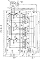
- [
FIG. 1] FIG. 1 is a block diagram schematically showing a circuit configuration of a motor control circuit according to the present invention. - [
FIG. 2] FIG. 2 is a block diagram schematically showing a form of wireless connection in an IGBT control board. - [
FIG. 3] FIG. 3 is a block diagram schematically showing a configuration of a power supply circuit. - [
FIG. 4] FIG. 4 is a layout drawing showing an example of a circuit layout of the IGBT control board. - [
FIG. 5] FIG. 5 is a layout drawing showing an example of a component layout on the IGBT control board. - [
FIG. 6] FIG. 6 is a block diagram schematically showing a structure of a conventional motor control device. - An embodiment of the present invention as exemplified by a motor control device for controlling a power motor of an electric vehicle or a hybrid vehicle will be described below. Referring to
FIGS. 1 to 3 , a circuit configuration of the motor control device will be explained first.FIG. 1 is a block diagram schematically showing a circuit configuration of the motor control circuit according to the present invention. As shown inFIG. 1 , the motor control device for controlling a three-phase AC motor 9 (referred to as a motor below as appropriate) is structured having anIGBT module 1, anIGBT control board 2, and a motor control board 3. - The
IGBT module 1 is formed with an inverter circuit that converts a direct current into a three-phase alternating current using an IGBT as a switching element. The inverter circuit, asFIG. 1 shows, is formed having six IGBTs 10 (and 11 to 16) andflywheel diodes 10a connected in parallel with therespective IGBTs 10. Note that the switching element is not limited to an IGBT, and the inverter circuit may also be structured using power transistors with various structures, such as a bipolar type, a field-effect type, and a MOS type. In the present embodiment, the inverter circuit has a module structure wherein theIGBT 10 and theflywheel diode 10a are mounted and integrated on a metal base via a ceramic insulating substrate. The inverter circuit is also formed with asensor circuit 10b (seeFIG. 2 ) for detecting an overcurrent in and overheating of theIGBT 10, which is integrated to structure theIGBT module 1. Further note that the inverter circuit may be formed by mounting theIGBT 10 and theflywheel diode 10a on an ordinary substrate. - In
FIG. 1 , respective arms of the inverter circuit are structured by oneIGBT 10. However, due to limitations such as a current capacity of the IGBT, a plurality of IGBTs may be arranged in parallel to structure one arm. Particularly in the case of an inverter circuit with a module structure, the circuit may be formed by mounting a bare chip on a metal base via a ceramic insulating substrate, and bare chips of a plurality of IGBTs are often arranged in parallel to structure one arm. Accordingly, the IGBT (switching element) on one arm does not necessarily mean a single IGBT as shown inFIG. 1 , and may indicate all the IGBTs connected in parallel on one arm. Furthermore, if one arm is formed by two IGBTs connected in parallel, then the two IGBTs may be controlled by one drive signal, or the respective IGBTs may be controlled by two drive signals. - A DC current with a positive-side voltage PV and a negative-side voltage NV (commonly a ground) is applied from a high-
voltage battery 55 serving as a high-voltage power source to the IGBT module, and converted into three-phase AC currents U, V, W. In cases where the motor 9 is a motor for powering an electric vehicle or a hybrid vehicle, a DC voltage of several hundred volts is input to theIGBT module 1. As shown inFIG. 1 , motor drive currents of the three phases, U-phase, V-phase and W-phase, are output from theIGBT module 1. These motor drive currents are output to the motor 9 via a cable, and connect with U-phase, V-phase and W-phase stator coils of the motor 9. - Formed on the motor control board 3 is a
motor control circuit 30 that operates at a much lower voltage than the power supply voltage of the inverter circuit. A DC current of around 12 volts, for example, is supplied from a low-voltage battery 75 serving as a low-voltage power source to the motor control board 3. Note that the low-voltage power source is not limited to the low-voltage battery 75, and may be structured from a DC-DC converter that decreases the voltage of the high-voltage battery 55, or the like. - The motor control board 3 is structured from the
motor control circuit 30, which controls the motor 9 in accordance with a command (external command) obtained by communication through a controller area network (CAN) or the like with an electronic control unit (ECU) (not shown) or the like that controls the running of a vehicle. Themotor control circuit 30 generates a drive signal for driving theIGBT 10 on respective arms of the inverter circuit controlling the motor 9. In the present embodiment, the switching element is an IGBT and a control terminal of the IGBT is a gate terminal. Therefore, the drive signal will be referred to as a gate drive signal. Also, themotor control circuit 30 receives detection signals from acurrent sensor 91 and arotation sensor 92, which detect behavior of the motor 9, and performs a feedback control depending on the operation status of the motor 9. - In
FIG. 1 , thecurrent sensor 91 is provided between theIGBT module 1 and the motor 9; however, thecurrent sensor 91 may be built into theIGBT module 1. Also, only currents of the two phases, U-phase and V-phase, are measured inFIG. 1 . A three-phase current of the U-phase, V-phase and W-phase is in a state of equilibrium and an instantaneous total sum thereof is zero. For this reason, a two-phase current is measured and the remaining one-phase current is found by computation. For therotation sensor 92, a resolver may be used. - The
motor control circuit 30 is formed with a microcomputer or digital signal processor (DSP) as a core component. An operating voltage of the microcomputer, DSP, or the like is generally 3.3 or 5 volts. Therefore, themotor control circuit 30 is also formed with a regulator circuit that generates an operating voltage from the 12-volt power supply voltage supplied from the low-voltage battery 75. - The
IGBT control board 2 is structured from agate drive circuit 20 that drives theIGBT 10 on respective arms of the inverter circuit, based on the gate drive signal generated in themotor control circuit 30. Also, theIGBT control board 2 is provided with a power supply circuit that supplies generated power from a low-voltage DC power source in themotor control circuit 30 to the gate drive circuit. The power supply circuit is formed from a transformer L serving as an insulation part IS (seeFIG. 2 ). As described in detail later, a photocoupler P that transmits the gate drive signal generated by themotor control circuit 30 to the gate drive circuit is mounted on theIGBT control board 2 and also serves as the insulation part IS (seeFIG. 2 ). Furthermore, theIGBT control board 2 is also structured from a powersource control circuit 27 for controlling the transformer L serving as the power supply circuit. - As described earlier in reference to
FIG. 1 , the inverter circuit formed on theIGBT module 1 is a high-voltage circuit 50 that operates at a high voltage, and themotor control circuit 30 formed on the motor control board 3 is a low-voltage circuit 70 that operates at a low voltage. TheIGBT control board 2 has both the high-voltage circuit 50 connected with theIGBT module 1, and the low-voltage circuit 70 connected with the motor control board 3. As described in detail later, the high-voltage circuit 50 and the low-voltage circuit 70 are disposed on theIGBT control board 2 having a predetermined insulation distance therebetween. The high-voltage circuit 50 and the low-voltage circuit 70 have a wireless connection achieved by the insulation part IS as mentioned above. -
FIG. 2 is a block diagram schematically showing a form of wireless connection in theIGBT control board 2. A form of wireless connection that corresponds to acircuit family 10A on one arm of the inverter circuit is shown here. Note that althoughFIG. 2 shows an example where one arm is formed having onecircuit family 10A, as explained above, one arm may be formed including a plurality ofIGBTs 10 and having a plurality ofcircuit families 10A. - The gate drive signal generated in the
motor control circuit 30 associated with the low-voltage circuit 70 is connected with an input terminal of the photocoupler P, which is an insulation part IS mounted in theIGBT control board 2. An output terminal of the photocoupler P is connected with adriver 20a of thegate drive circuit 20, which is mounted in a high-voltage circuit area 5 of theIGBT control board 2 associated with the high-voltage circuit 50. The high-voltage circuit area 5 of theIGBT control board 2 will be described later. The photocoupler P is provided with an input-side light-emitting diode, and an output-side photodiode or phototransistor, and is a commonly known insulation part that uses light to wirelessly transmit a signal from the input side to the output side. Due to the photocoupler P, the gate drive signal is transmitted from themotor control circuit 30 to thegate drive circuit 20 while an insulated state is maintained between the low-voltage circuit 70 and the high-voltage circuit 50. Thedriver 20a of thegate drive circuit 20 drivingly controls theIGBT 10 of theIGBT module 1 associated with the high-voltage circuit 50. - Incidental to the above-described
IGBT 10 is asensor circuit 10b for detecting an overcurrent and overheating. AsFIG. 2 shows, in the present example, thesensor circuit 10b is formed having atemperature sensor 10c and anovercurrent detector 10d. Thetemperature sensor 10c is a thermostat or a diode, and a change in voltage between terminals due to the temperature is detected by adiagnostic circuit 20b of thegate drive circuit 20. Theovercurrent detector 10d, for example, detects a minute current proportional to a large current flowing through theIGBT 10, wherein the proportion is approximately 1/1,000,000 to 1/100,000, and thereby detects when the large current flowing through theIGBT 10 exceeds a predetermined value. A detection result thereof is received by thediagnostic circuit 20b. - The
diagnostic circuit 20b determines an overheated state when the voltage between the terminals of thetemperature sensor 10c falls below a predetermined value. If a detection result indicating an abnormality is received from theovercurrent detector 10d, then an overcurrent state caused by a short circuit or the like is determined. When at least one of either an overheated state or an overcurrent state is determined, thediagnostic circuit 20b outputs a diagnostic signal. Based on the diagnostic signal, thedriver 20a controls theIGBT 10 to an off state regardless of the status of the gate drive signal received from themotor control circuit 30 via the photocoupler P. - The diagnostic signal is also transmitted to the
motor control circuit 30. Thediagnostic circuit 20b is part of the high-voltage circuit 50 formed in the high-voltage circuit area 5 of theIGBT control board 2. Accordingly, the diagnostic signal is wirelessly transmitted to themotor control circuit 30 via the photocoupler P serving as the insulation part IS. The cause of the abnormality, whether overheating, an overcurrent or the like, is not transmitted to themotor control circuit 30; however, it is possible to at least know that an abnormality has occurred. Themotor control circuit 30 then performs processing to respond to the abnormality, such as processing to stop the motor 9. - As mentioned above, the voltage between the terminals of the
temperature sensor 10c can be measured by thediagnostic circuit 20b. Therefore, atemperature detection circuit 20c that detects the temperature can be provided in thediagnostic circuit 20b or in the vicinity of thediagnostic circuit 20b.FIG. 2 shows an example where thetemperature detection circuit 20c is provided in the vicinity of thediagnostic circuit 20b. There is no need to provide thetemperature detection circuit 20c incidental to thegate drive circuit 20 that corresponds to all the arms of the inverter circuit, and thetemperature detection circuit 20c is thus shown by a dashed line inFIG. 2 . Thetemperature detection circuit 20c is provided in the high-voltage circuit area 5 of theIGBT control board 2, and therefore the detection result is wirelessly transmitted to themotor control circuit 30 in a manner similar to the diagnostic signal via the photocoupler P serving as the insulation part IS. - As described above, the
IGBT control board 2 is provided with a power supply circuit that supplies generated power from a low-voltage DC power source in themotor control circuit 30 to the gate drive circuit.FIG. 3 is a block diagram schematically showing a configuration of the power supply circuit. The power supply circuit will be explained below with reference toFIGS. 1 to 3 . - The power supply circuit is formed from the transformer L serving as the insulation part IS. A primary voltage V1 is stabilized to a constant voltage in a voltage regulator circuit of the motor control circuit 30 (motor control board 3), that is, the low-
voltage circuit 70, and supplied to the transformer L. Although the motor control board 3 is supplied with a 12-volt power supply voltage, for example, as mentioned above, the voltage of thebattery 75 fluctuates depending on a load. Hence, using a step-up regulator or a step-down regulator to serve as the voltage regulator circuit, the constant voltage of the primary voltage V1 is raised to approximately 15 to 18 volts or lowered to approximately 8 to 10 volts, for example, and then supplied to the transformer L. - Regarding the transformer L, in the present embodiment six transformers L1 to L6 are provided respectively corresponding to the six arms of the inverter circuit. Secondary voltages V21 to V26 are output from the transformers L1 to L6, respectively. The transformers L1 to L6 have practically identical structures and output secondary voltages V2 of approximately identical voltage. In
FIG. 3 , diodes D1 to D12 are rectifying diodes, condensers C1 to C6 are smoothing condensers, and a condenser C7 is a condenser for stabilizing the primary voltage. - The
IGBT control board 2 is formed with the powersource control circuit 27 associated with the low-voltage circuit 70, and controls the transformer L serving as the power supply circuit. The powersource control circuit 27 is formed havingtransistors 27b and 27c that control a voltage applied by a primary-side coil, and a control circuit 27a that controls thetransistors 27b and 27c. The powersource control circuit 27 according to the present embodiment adopts a push-pull type configuration. Six transformers L are provided corresponding to the six arms of the inverter circuit, and the powersource control circuit 27 collectively controls all the transformers L1 to L6. Also, as described above, the primary voltage V1 for the transformer L is stabilized, and therefore a secondary voltage V2 is determined by a ratio of transformation of the transformer L without the secondary voltage V2 being fed back to the primary side. - The transformer L is a commonly known insulation part that electromagnetically joins the primary-side coil and a secondary-side coil to transmit a signal and energy. Accordingly, a power supply voltage can be supplied to the
gate drive circuit 20 and the like while maintaining insulation between the low-voltage circuit 70 and the high-voltage circuit 50. - As explained above, the
IGBT control board 2 includes both the high-voltage circuit 50 and the low-voltage circuit 70, and maintains insulation therebetween by wirelessly joining both circuits using the insulation part IS. Referring toFIGS. 4 and5 , a specific layout of theIGBT control board 2 will be explained below.FIG. 4 is a layout drawing showing an example of a circuit layout of theIGBT control board 2, andFIG. 5 is a layout drawing showing an example of a specific component layout on theIGBT control board 2. - As
FIGS. 4 and5 illustrate, theIGBT control board 2 has a low-voltage circuit area 7 generally formed into a T shape whose head lies at the left side in the figures. Aconnector 48 is provided in the low-voltage circuit area 7 at the head of the T shape, i.e., the upper left side in the figures. Theconnector 48 is connected with the above-described motor control board 3 by a harness (not shown). The gate drive signal corresponding to respective arms of the inverter circuit is transmitted from themotor control circuit 30 to the low-voltage circuit area 7 of theIGBT control board 2 via theconnector 48. The power supply voltage operating the powersource control circuit 27 and the primary-side voltage V1 for the transformer L are also transmitted from the motor control board 3 via theconnector 48. As shown inFIG. 5 , a low-voltage circuit 28 is formed below theconnector 48 in the figure, and a driver circuit and a receiver circuit are the input and output signals via theconnector 48. Furthermore, the primary voltage for the transformer L may be generated in the low-voltage circuit 28. - The high-
voltage circuit area 5 is also formed on theIGBT control board 2. Six high-voltage circuit areas 5 are formed corresponding to the respective arms of the inverter circuit. The high-voltage circuit areas 5 as mentioned above have at least onegate drive circuit 20 for driving theIGBT 10 included on the respective arms. As shown inFIG. 2 , in the present example, thegate drive circuit 20 and onecircuit family 10A of one arm are connected by five signal wires. TheIGBT module 1 has a terminal-connecting pin corresponding to these signal wires. Thegate drive circuit 20 and thecircuit family 10A are connected by solder welding the pin to a throughhole 4 of theIGBT control board 2 as illustrated inFIGS. 4 and5 . Note that in the present embodiment, one arm of the inverter circuit is structured connecting twoIGBTs 10 in parallel. In other words, one arm is provided with twocircuit families 10A, and onegate drive circuit 20 is connected with twocircuit families 10A. Therefore, onegate drive circuit 20 is provided with ten throughholes 4. - Regarding the high-
voltage circuit area 5, a plurality of high-voltage circuit areas 5 are disposed aligned on both sides (e.g. three to a side in the present example) of the low-voltage circuit area 7 such that a portion of the low-voltage circuit area 7 corresponding to the trunk portion of a T shape is provided therebetween. In such case, thegate drive circuit 20 is disposed with a predetermined insulation distance d1 provided between thegate drive circuit 20 and the low-voltage circuit area 7. Thegate drive circuit 20 is further disposed with a predetermined insulation distance d2 or d3 provided between adjacentgate drive circuits 20. By providing the predetermined insulation distance d1 between thegate drive circuit 20 and the low-voltage circuit area 7, aninsulation area 6 is formed along the low-voltage circuit area 7. By further providing the predetermined insulation distance d2 or d3 between adjacentgate drive circuits 20, a comb-shapedinsulation area 6 is formed on both sides of the low-voltage circuit area 7 with the trunk portion side of the T-shaped low-voltage circuit area 7 serving as a base portion thereof. - The transformers L1 to L6 serving as power supply circuits are provided straddling the
insulation area 6 formed along the trunk portion of the T-shaped low-voltage circuit area 7, and the low-voltage circuit area 7 and the respective high-voltage circuit areas 5 are each joined in an insulated state. Namely, the primary-side voltage V1 is applied to the low-voltage circuit area 7 of the transformers L1 to L6, and the secondary-side voltage V2 is output to the high-voltage circuit areas 5 of the transformers L1 to L6. The high-voltage secondary-side voltage V2 only appears on the side ofgate drive circuits 21 to 26 in the high-voltage circuit areas 5 corresponding to the transformers L1 to L6. Therefore, high-voltage wiring is not drawn out over a long distance within theIGBT control board 2. As a consequence, there is no need to increase the surface area of theinsulation area 6, where no parts for securing insulation distance can be mounted, and the substrate can be effectively utilized. - The transformers L1 to L6 are controlled by a common power
supply control circuit 27 formed on the low-voltage circuit area 7. It is thus possible to keep the surface area of theIGBT control board 2 down and achieve a more compact motor control device. In addition, as shown inFIGS. 4 and5 , the powersource control circuit 27 is arranged at a general central portion among the plurality of transformers L1 to L6. Therefore, a maximum wire length among wiring connecting the powersource control circuit 27 and the transformers L1 to L6, e.g. a wire length to the transformer L4 or L3, can be shortened. A longer wire tends to generate more noise; however, since the maximum wiring length can be kept shorter, noise generation can be suppressed as well. Naturally, it is also possible to suppress the total wiring length that is the sum of the wiring lengths to the transformers L1 to L6. A larger amount of wiring tends to generate more noise, but keeping the total wiring length down can help suppress noise generation. Moreover, since the wiring lengths from the powersource control circuit 27 to the transformers L1 to L6 are uniform, it is possible to uniform power source characteristics of the secondary-side voltage V2 (V21 to V26) of the transformers L1 to L6, whereby the operation of thegate drive circuit 20 and the inverter circuit can be stabilized. - The photocouplers P (P11, P21, P31, P41, P51, P61) serving as insulation parts for signal transmission are provided straddling the
insulation area 6 formed along the trunk portion of the T-shaped low-voltage circuit area 7. These photocouplers P are disposed aligned with the transformers L1 to L6 along a boundary line where the low-voltage circuit area 7 and the high-voltage circuit area 5 face one another. Since the insulation parts IS that connect the low-voltage circuit area 7 and the high-voltage circuit area 5 are disposed arranged in a row, providing the minimum requiredinsulation area 6 on theIGBT control board 2 is sufficient. - Due to the photocouplers P, gate drive signals generated by the
motor control circuit 30 and corresponding to the respective arms are joined between the low-voltage circuit area 7 and the high-voltage circuit areas (gate drive circuits 21 to 26) in an insulated state. In other words, gate drive signals generated at a power supply voltage lower than the power supply voltage of the inverter circuit are wirelessly transmitted from the low-voltage circuit area 7 to the respectivegate drive circuits 21 to 26 of the high-voltage circuit area 5. The gate drive signals are transmitted from thegate drive circuits 21 to 26 to theIGBTs 10, whereby theIGBTs 10 are controlled. - Additional photocouplers P (P12, P22, P32, P42, P52, P62) serving as insulation parts for signal transmission are also provided straddling the
insulation area 6 formed along the trunk portion of the T-shaped low-voltage circuit area 7. A feedback signal sent from the inverter circuit to therespective drive circuits 21 to 26 by these photocouplers P is wirelessly transmitted from the high-voltage circuit area 5 to the low-voltage circuit area 7. - These photocouplers P are disposed aligned with the transformers L1 to L6 and the photocouplers P (P11, P21, P31, P41, P51, P61) that transmit the gate drive signal, along a boundary line where the low-
voltage circuit area 7 and the high-voltage circuit area 5 face one another. Since the insulation parts IS that connect the low-voltage circuit area 7 and the high-voltage circuit area 5 are disposed arranged in a row, providing the minimum requiredinsulation area 6 on theIGBT control board 2 is sufficient. When increasing insulation performance by providing a slit in theinsulation area 6 on theIGBT control board 2, linear processing on a lower surface of the transformer L and the photocoupler P, i.e., theinsulation area 6 along the boundary line, enables the formation of a slit. - As described above, the
gate drive circuit 20 is provided corresponding to the respective arms of the inverter circuit. The correspondence between thegate drive circuit 20 and the respective arms will be explained below, wherein an arm connected with the positive-side voltage PV from the DC power source of the inverter circuit is referred to as an upper-level arm, and an arm connected with the negative-side voltage NV is referred to as a lower-level arm. - The
IGBT 11 on a U-phase upper-level arm is driven by thegate drive circuit 21; theIGBT 12 on a V-phase upper-level arm is driven by thegate drive circuit 22; theIGBT 13 on a W-phase upper-level arm is driven by thegate drive circuit 23; theIGBT 14 on a U-phase lower-level arm is driven by thegate drive circuit 24; theIGBT 15 on a V-phase lower-level arm is driven by thegate drive circuit 25; and theIGBT 16 on a W-phase lower-level arm is driven by thegate drive circuit 26. Thegate drive circuits 21 to 23 are referred to as upper-level gate drive circuits (upper-level drive circuits), and thegate drive circuits 24 to 26 are referred to as lower-level gate drive circuits (lower-level drive circuits) below as appropriate. - As
FIGS. 4 and5 illustrate, among thegate drive circuits 21 to 26, the upper-levelgate drive circuits 21 to 23 driving theIGBTs 11 to 13 on the upper-level arms are arranged aligned on a side of the low-voltage circuit area 7, namely, an upper side in the figures. The lower-levelgate drive circuits 24 to 26 driving theIGBTs 14 to 16 on the lower-level arms are arranged aligned on another side of the low-voltage circuit area 7, namely, a lower side in the figures. - As shown in
FIG. 1 , in the inverter circuit, theIGBTs 11 to 13 on the upper-level arms are connected with the positive-side voltage PV of the DC power source, and theIGBTs 14 to 16 on the lower-level arms are connected with the negative-side voltage NV of the DC power source. Arranging theIGBTs 11 to 13 on the upper-level arms and theIGBTs 14 to 16 on the lower-level arms in respective rows thus facilitates connection with the positive-side voltage PV and the negative-side voltage NV. As a consequence, arranging thedrive circuit 20 driving theIGBT 10 according to the respective rows of the upper-levelgate drive circuits 21 to 23 and the lower-levelgate drive circuits 24 to 26 also helps enable efficient wiring. - As explained above, the
gate drive circuit 20 is disposed with the predetermined insulation distance d2 or d3 provided between adjacentgate drive circuits 20. Specifically, the upper-levelgate drive circuits 21 to 23 are disposed with the predetermined insulation distance d2 provided between adjacent gate drive circuits, and the lower-level drive circuits 24 to 26 are disposed with the predetermined insulation distance d3 provided between adjacent gate drive circuits. Here, the insulation distance d2 is a longer distance than the insulation distance d3 (seeFIG. 4 ). In other words, the insulation distance d2 provided between adjacent upper-levelgate drive circuits 21 to 23 is set longer than the insulation distance d3 provided between adjacent lower-levelgate drive circuits 24 to 26. - For the
IGBTs 11 to 13 on the upper-level arms connected with the high positive-side voltage PV among the DC power source voltage of the inverter circuit, a potential of an emitter terminal when in an on state increases to near the voltage PV. Since theIGBTs 14 to 16 on the lower-level arms are connected with the low negative-side voltage NV (commonly a ground), the emitter terminal when in an on state is the negative-side voltage NV. AsFIGS. 1 and2 show, thegate drive circuit 20 drives theIGBT 10 by controlling a difference in potential between two terminals, the emitter terminal and the gate terminal of theIGBT 10. Thus, the potential of the upper-levelgate drive circuits 21 to 23 connected with theIGBTs 11 to 13 on the upper-level arms increases to near the voltage PV when theIGBTs 11 to 13 are in an on state. Hence, by setting the insulation distance d2 to a longer distance than the insulation distance d3, a sufficient insulation distance is secured between the upper-levelgate drive circuits gate drive circuits 24 to 26 is not limited provided that a minimum insulation distance is secured for ensuring that a large current flowing through the wiring of a potential NV in theIGBT module 1 does not flow in via the throughhole 4. -
Reference numeral 8 inFIGS. 4 and5 indicates a through hole through which a fixing member for fixing theIGBT control board 2 runs. A metal bolt, for example, is used for the fixing member. A common structure is one in which throughholes 81 to 84 for fixing the substrate are provided at the four corners of theIGBT control board 2. In the present embodiment, four throughholes 85 to 88 are further provided. These four throughholes 85 to 88 are provided in the vicinity of a center line of the oblong substrate. Since a large current flows through the high-voltage circuit area 5, the transformer L, and the like, theIGBT control board 2 tends to become heated, and there is a risk of deformation such as warpage occurring on the substrate due to excessive heating. However, by also providing the throughholes 85 to 88 at a central portion of the substrate in addition to the throughholes 81 to 84 at the four corners of the substrate, it is possible to suppress warpage and reliably fix theIGBT control board 2. Moreover, a high vibration resistance required for in-vehicle use can be secured. - The through holes 85 to 87 are provided within the constant-
voltage circuit area 7 with a predetermined insulation distance secured. In cases where a metal bolt is used as the fixing member, by providing the throughhole 8 through which the bolt runs within the low-voltage circuit area 7 rather than the high-voltage circuit area 5, insulation can be secured with the use of a short insulation distance. In other words, providing more throughholes 8 than normally used makes it possible to suppress an increase in the surface area of the substrate. In addition, the throughholes voltage circuit area 7 and disposed more toward one side of the high-voltage circuit areas 5, which are disposed aligned on both sides of the low-voltage circuit area 7 such that the low-voltage circuit area 7 is provided therebetween. AsFIG. 5 shows, the powersource control circuit 27 and the like can be disposed at suitable positions without interfering with the mounting of components on the low-voltage circuit area 7. - In the present embodiment, the through
holes voltage circuit area 7 towards the upper-levelgate drive circuits 21 to 23 side, as shown inFIGS. 4 and5 . The reason for this will be explained below. - As mentioned above, the high-
voltage circuit area 5 where the lower-levelgate drive circuits 24 to 26 are provided may have a shorter insulation distance than that of the upper-levelgate drive circuits 21 to 23. Therefore, more components can be mounted in these high-voltage circuit areas 5 compared to the high-voltage circuit areas 5 provided with the upper-levelgate drive circuits 21 to 23 in an amount corresponding to the reduced insulation area. For example, additional circuits such as atemperature detection sensor 20c can be provided in the high-voltage circuit area 5 along with the lower-levelgate drive circuits 24 to 26. - When the output of an additional circuit in the high-
voltage circuit area 5 is transmitted to the low-voltage circuit area 7 and transferred to themotor control circuit 30 via theconnector 48, a control can be achieved in themotor control circuit 30 that uses a processing result of the additional circuit. In order to transmit the output of the additional circuit from the lower-levelgate drive circuits 24 to 26 to the low-voltage circuit area 7, a signal-transmitting insulation part such as a photocoupler must be mounted straddling theinsulation area 6. Providing the throughholes gate drive circuits 24 to 26 side takes up space that could be used for mounting such an additional signal-transmitting insulation part. However, by providing the throughholes gate drive circuits 21 to 23 side, a space is secured for mounting an additional signal-transmitting insulation part. - Furthermore, as
FIGS. 4 and5 show, the throughholes gate drive circuits 21 to 23 within the low-voltage circuit area 7, and also arranged at a positions along theinsulation area 6 between thegate drive circuits gate drive circuits holes gate drive circuits 21 to 23 side, a sufficient insulation distance is secured between the upper-levelgate drive circuits 21 to 23. - The present embodiment illustrated an example where a
temperature detection circuit 20c, which detects the temperature of theIGBT 15 based on a detection result of thetemperature sensor 10c detecting the temperature of at least oneIGBT 15, is provided in the high-voltage circuit area 5 along with the lower-levelgate drive circuit 25. In a state with no abnormal excessive heating, all the IGBTs 10 exhibit similar temperature increase trends. Therefore, measuring the temperature of any one of theIGBTs 10 is sufficient. Also, a difference due to the placement of theIGBT 10 can be corrected in themotor control circuit 30 by preparing in advance a map or the like for correcting an error caused by placement. - The detection result of the
temperature detection circuit 20c is transmitted from thegate drive circuit 25 of the high-voltage circuit area 5 to the low-voltage circuit area 7. As shown inFIG. 4 , the photocoupler P (P53) serving as a signal-transmitting insulation part is provided straddling theinsulation area 6 formed along the low-voltage circuit area 7. The photocoupler P53 is disposed aligned with the transformer L5 and the photocouplers P51, P52 of thegate drive circuit 25 provided with thetemperature detection circuit 20c, along the boundary line where the low-voltage circuit area 7 and the high-voltage circuit area 5 face one another. In the present embodiment, the throughholes voltage circuit area 7 towards the upper-levelgate drive circuits 21 to 23 side, as shown inFIGS. 4 and5 . Therefore, a space for mounting the photocoupler P53, i.e., an additional signal-transmitting insulation part, can be well secured. - In this manner, four insulation parts IS the connect the low-
voltage circuit area 7 and the high-voltage circuit area 5 are disposed arranged in a row. Accordingly, mounting the photocoupler P53 does not increase the surface area of theinsulation area 6 of theIGBT control board 2. Also, as explained above, when increasing insulation performance by providing a slit in theinsulation area 6 on theIGBT control board 2, linear processing on a lower surface of the transformer L and the photocoupler P, i.e., theinsulation area 6 along the boundary line, enables the formation of a slit. - As described using the specific layout above, the
IGBT control board 2 includes both the high-voltage circuit 50 and the low-voltage circuit 70, and maintains insulation therebetween by wirelessly joining both circuits using the insulation part IS. Therefore, insulation is secured with asmall insulation area 6, whereby a compact size is achieved. Accordingly, it is possible to provide a control device for an AC motor that is capable of securing insulation between a low-voltage circuit and a high-voltage circuit, while also achieving a compact size. - The present invention can be applied to a motor control device that controls an AC motor used for powering an electric vehicle, hybrid vehicle, or the like.
- [
FIG. 1 ] - 1/ IGBT MODULE
- 92/ ROTATION SENSOR
- 2/ IGBT CONTROL BOARD
- 20/ GATE DRIVE CIRCUIT
- IS/ INSULATION PART
- 27/ POWER SOURCE CONTROL CIRCUIT
- 30/ MOTOR CONTROL CIRCUIT
- 3/ MOTOR CONTROL BOARD
- [
FIG. 2 ] - 1/ IGBT MODULE
- 10b/ SENSOR CIRCUIT
- 10c/ TEMPERATURE SENSOR
- 10d/ OVERCURRENT DETECTOR
- 5/ HIGH-VOLTAGE CIRCUIT AREA
- 20c/ TEMPERATURE DETECTION CIRCUIT
- 20b/ DIAGNOSTIC CIRCUIT
- 20a/ DRIVER L/ TRANSFORMER
- P/ PHOTOCOUPLER
- 27/ POWER SOURCE CONTROL CIRCUIT
- 30/ MOTOR CONTROL CIRCUIT
- [
FIG. 3 ] - 27/ POWER SOURCE CONTROL CIRCUIT
- 27a/ CONTROL CIRCUIT
- LOW-VOLTAGE CIRCUIT ↔ HIGH-VOLTAGE CIRCUIT
- [
FIG. 4 ] - 21/ GATE DRIVE CIRCUIT (U-PHASE UPPER LEVEL)
- 22/ GATE DRIVE CIRCUIT (V-PHASE UPPER LEVEL)
- 23/ GATE DRIVE CIRCUIT (W-PHASE UPPER LEVEL)
- 27/ POWER SOURCE CONTROL CIRCUIT
- 24/ GATE DRIVE CIRCUIT (U-PHASE LOWER LEVEL)
- 20c/ TEMPERATURE DETECTION CIRCUIT
- 25/ GATE DRIVE CIRCUIT (V-PHASE LOWER LEVEL)
- 26/ GATE DRIVE CIRCUIT (W-PHASE LOWER LEVEL)
- [
FIG. 6 ] - 100/ INVERTER CIRCUIT
- 200/ IGBT DRIVE CIRCUIT
- 300/ MOTOR CONTROL CIRCUIT
- GATE DRIVE CIRCUIT
Claims (10)
- A motor control device, characterized by comprising a drive circuit (20) that is respectively provided on arms of an inverter circuit supplying current to an AC motor (9), and that drives a switching element (10) included on the arms; and
a power source control circuit (27) that performs a control of a power supply circuit for supplying power to the drive circuit, the motor control device further comprising:a low-voltage circuit area (7) that includes the power source control circuit;a high-voltage circuit area (5) that includes one drive circuit (20), wherein a plurality of the high-voltage circuit areas (5) is disposed aligned on both sides of the low-voltage circuit area (7) such that the low-voltage circuit area (7) is provided therebetween and also disposed with a predetermined insulation distance (d1) provided between the high-voltage circuit area (5) and the low-voltage circuit area (7); anda transformer (L1-L6) that serves as the power supply circuit and respectively joins the low-voltage circuit area and the high-voltage circuit areas in an insulated state, the transformer (L1-L6) being provided straddling an insulation area (6) which is formed along both sides of the low voltage circuit area (7) ;wherein, as the drive circuit (20), a plurality of upper-level drive circuits (21-23) that drive the switching element on a plurality of upper-level arms connected with a positive side (PV) of a DC power source (55) of the inverter circuit is arranged aligned on a side of the low-voltage circuit area (7) and a plurality of lower-level drive circuits (24-26) that drive the switching element on a plurality of lower-level arms connected with a negative side (NV) of the DC power source (55) of the inverter circuit is arranged aligned on another side of the low-voltage circuit area (7). - The motor control device according to claim 1, wherein
the drive circuit is disposed with a predetermined insulation distance (d2, d3) provided between adjacent drive circuits (20). - The motor control device according to claim 1, wherein
an insulation distance (d2) provided between adjacent upper-level drive circuits (21-23) is set longer than an insulation distance (d3) provided between adjacent lower-level drive circuits (24-26). - The motor control device according to claim 3, wherein
a temperature detection circuit (20c), which detects a temperature of the switching element based on a detection result of a temperature sensor detecting a temperature of at least one switching element (10), is provided in the high-voltage circuit area (5) along with the lower-level drive circuit (24-26). - The motor control device according to claim 4, further comprising:a signal-transmitting insulation part (P, P53) that wirelessly transmits the detection result of the temperature detection circuit from the high-voltage circuit area (5) to the low-voltage circuit area (7), whereinthe signal-transmitting insulation part is disposed aligned with the transformer (L5) in the high-voltage circuit area provided with the temperature detection circuit, along a boundary line where the low-voltage circuit area and the high-voltage circuit area face one another.
- The motor control device according to any one of claims 1 to 5, further comprising:a through hole (86, 87) through which a fixing member for fixing a substrate runs, whereinthe through hole is provided within the low-voltage circuit area (7) toward the upper-level drive circuit (21-23) side.
- The motor control device according to any one of claims 1 to 6, further comprising:a signal-transmitting insulation part (P) that wirelessly transmits from the low-voltage circuit area (7) to the high-voltage circuit area (5) drive signals generated at a voltage lower than a power source voltage of the inverter circuit (50) for driving the switching element (10) included on the arms, whereinthe signal-transmitting insulation part is disposed aligned with the transformer, along a boundary line where the low-voltage circuit area and the high-voltage circuit area face one another.
- The motor control device according to any one of claims 1 to 7, further comprising:a signal-transmitting insulation part that wirelessly transmits a feedback signal from the inverter circuit (50) to the drive circuits (20) from the high-voltage circuit area (5) to the low-voltage circuit area (7), whereinthe signal-transmitting insulation part is disposed aligned with the transformer, along a boundary line where the low-voltage circuit area and the high-voltage circuit area face one another.
- The motor control device according to any one of claims 1 to 8, wherein the power source control circuit (27) is arranged at a generally central portion among a plurality of the transformers (L1-L6).
- The motor control device according to any one of claims 1 to 3, further comprising:a through hole (86, 87) through which a fixing member for fixing a substrate runs, whereinthe through hole is provided within the low-voltage circuit area toward any one side of the high-voltage circuit areas (5) disposed aligned on both sides of the low-voltage circuit area such that the low-voltage circuit area (7) is provided therebetween.
Applications Claiming Priority (2)
| Application Number | Priority Date | Filing Date | Title |
|---|---|---|---|
| JP2007300611A JP5029900B2 (en) | 2007-11-20 | 2007-11-20 | Motor control device |
| PCT/JP2008/069436 WO2009066546A1 (en) | 2007-11-20 | 2008-10-27 | Motor control device |
Publications (3)
| Publication Number | Publication Date |
|---|---|
| EP2157689A1 EP2157689A1 (en) | 2010-02-24 |
| EP2157689A4 EP2157689A4 (en) | 2015-05-20 |
| EP2157689B1 true EP2157689B1 (en) | 2017-03-01 |
Family
ID=40667373
Family Applications (1)
| Application Number | Title | Priority Date | Filing Date |
|---|---|---|---|
| EP08851581.2A Active EP2157689B1 (en) | 2007-11-20 | 2008-10-27 | Motor control device |
Country Status (6)
| Country | Link |
|---|---|
| US (1) | US8093852B2 (en) |
| EP (1) | EP2157689B1 (en) |
| JP (1) | JP5029900B2 (en) |
| KR (1) | KR101177719B1 (en) |
| CN (1) | CN101682291B (en) |
| WO (1) | WO2009066546A1 (en) |
Cited By (1)
| Publication number | Priority date | Publication date | Assignee | Title |
|---|---|---|---|---|
| US11848619B2 (en) | 2020-01-21 | 2023-12-19 | Itt Manufacturing Enterprises Llc | Apparatus and methods for supplying DC power to control circuitry of a matrix converter |
Families Citing this family (83)
| Publication number | Priority date | Publication date | Assignee | Title |
|---|---|---|---|---|
| JP5359604B2 (en) * | 2009-06-26 | 2013-12-04 | 株式会社デンソー | Control device for power conversion circuit |
| JP4831246B2 (en) * | 2009-09-08 | 2011-12-07 | 株式会社デンソー | Power converter |
| US8644044B2 (en) * | 2009-10-14 | 2014-02-04 | General Electric Company | Power electronics and integration system for providing a common high current inverter for use with a traction inverter and an auxiliary inverter |
| US8203232B2 (en) * | 2009-12-10 | 2012-06-19 | Lear Corporation | Embedded wireless communications for electronic control unit having multiple ground references |
| JP5423536B2 (en) * | 2010-03-31 | 2014-02-19 | 株式会社デンソー | Power converter |
| JP5389730B2 (en) * | 2010-05-14 | 2014-01-15 | 株式会社デンソー | Discharge device for power conversion system |
| CN101916984B (en) * | 2010-07-15 | 2015-09-23 | 芜湖莫森泰克汽车科技有限公司 | A kind of IGBT intelligent driving module for new energy automobile and control method thereof |
| JP5622043B2 (en) * | 2010-09-15 | 2014-11-12 | アイシン・エィ・ダブリュ株式会社 | Inverter device |
| JP5733945B2 (en) * | 2010-10-15 | 2015-06-10 | 三菱重工業株式会社 | Inverter module and inverter-integrated electric compressor |
| JP5556584B2 (en) * | 2010-10-26 | 2014-07-23 | トヨタ自動車株式会社 | Inverter drive |
| JP5500553B2 (en) * | 2010-11-02 | 2014-05-21 | 三菱電機株式会社 | Gate drive device |
| JP5472043B2 (en) * | 2010-11-04 | 2014-04-16 | 株式会社デンソー | Driving device for power conversion circuit |
| JP5510292B2 (en) * | 2010-11-30 | 2014-06-04 | 富士電機株式会社 | Gate drive power supply and inverter control circuit |
| CN102163907B (en) * | 2011-01-28 | 2014-03-12 | 中国电力科学研究院 | Voltage source inverter basic function unit based on total control device |
| JP6104512B2 (en) | 2011-04-01 | 2017-03-29 | ローム株式会社 | Temperature detection device |
| JP5413407B2 (en) * | 2011-06-03 | 2014-02-12 | 株式会社デンソー | Electronic equipment |
| JP5660388B2 (en) * | 2011-06-07 | 2015-01-28 | 株式会社デンソー | Power converter |
| JP2013027282A (en) * | 2011-07-26 | 2013-02-04 | Denso Corp | Power converter |
| JP5669686B2 (en) * | 2011-07-27 | 2015-02-12 | 株式会社日立製作所 | Gate drive device for switching element |
| JP5942371B2 (en) * | 2011-09-21 | 2016-06-29 | 富士通株式会社 | Compound semiconductor device and manufacturing method thereof |
| JP5639978B2 (en) | 2011-09-27 | 2014-12-10 | 日立オートモティブシステムズ株式会社 | Automotive power conversion control device |
| JP5865715B2 (en) * | 2012-01-25 | 2016-02-17 | 三菱電機株式会社 | Motor control device |
| WO2013179638A1 (en) * | 2012-05-29 | 2013-12-05 | 日本精工株式会社 | Semiconductor module and production method for same |
| JP5664600B2 (en) * | 2012-06-27 | 2015-02-04 | トヨタ自動車株式会社 | Electric car |
| US9467086B2 (en) * | 2012-07-12 | 2016-10-11 | Mitsubishi Electric Corporation | Vehicle-mounted motor driving control board |
| CN103812312B (en) * | 2012-11-08 | 2016-08-24 | 中车大同电力机车有限公司 | AuCT buck chopper power model driving means |
| CN103227628B (en) * | 2013-01-30 | 2017-02-08 | 深圳市航盛电子股份有限公司 | IGBT (Insulated Gate Bipolar Transistor) drive module for electric automobile |
| US20140285123A1 (en) * | 2013-03-15 | 2014-09-25 | James Tomlinson | Solar A/C Direct Motor Drive |
| JP6229148B2 (en) * | 2013-05-30 | 2017-11-15 | パナソニックIpマネジメント株式会社 | Inverter device and motor drive device |
| EP2821274B1 (en) * | 2013-06-28 | 2019-05-08 | LG Electronics Inc. | Driving apparatus for electric vehicle |
| JP6337394B2 (en) * | 2013-07-05 | 2018-06-06 | パナソニックIpマネジメント株式会社 | Semiconductor device |
| JP2015073261A (en) * | 2013-09-03 | 2015-04-16 | ルネサスエレクトロニクス株式会社 | Semiconductor device |
| JP5842888B2 (en) * | 2013-09-24 | 2016-01-13 | 株式会社デンソー | Isolated power supply |
| JP5910595B2 (en) * | 2013-09-24 | 2016-04-27 | 株式会社デンソー | Isolated power supply |
| JP6058148B2 (en) * | 2013-09-26 | 2017-01-11 | 三菱電機株式会社 | Power converter and air conditioner |
| JP6184507B2 (en) * | 2013-10-09 | 2017-08-23 | 日立オートモティブシステムズ株式会社 | Driver board and power conversion device |
| JP6171858B2 (en) * | 2013-11-06 | 2017-08-02 | 株式会社デンソー | Isolated power supply |
| US20150349623A1 (en) * | 2014-06-03 | 2015-12-03 | Hyundai Motor Company | Inverter gate board |
| JP6172061B2 (en) * | 2014-06-12 | 2017-08-02 | 株式会社デンソー | Power supply device for power conversion circuit |
| EP2996449B1 (en) * | 2014-09-11 | 2017-11-29 | Siemens Aktiengesellschaft | Frequency converter assembly with a multiphase frequency converter |
| JP6237554B2 (en) * | 2014-09-24 | 2017-11-29 | アイシン・エィ・ダブリュ株式会社 | Power conversion device control board |
| JP6379965B2 (en) * | 2014-10-09 | 2018-08-29 | 株式会社デンソー | Power converter |
| JP6408857B2 (en) * | 2014-10-20 | 2018-10-17 | ローム株式会社 | Gate driver unit and power module |
| EP3229361B1 (en) * | 2014-12-03 | 2019-06-19 | Nissan Motor Co., Ltd | Power conversion device |
| JP5843299B1 (en) * | 2015-01-13 | 2016-01-13 | 有限会社アイ・アール・ティー | Inverter drive |
| JP2017022798A (en) * | 2015-07-07 | 2017-01-26 | ルネサスエレクトロニクス株式会社 | Electric power conversion equipment and driving device |
| CN105071643A (en) * | 2015-07-27 | 2015-11-18 | 焦作华飞电子电器股份有限公司 | Wireless power supply method for high-voltage isolated SCR and IGBT driver |
| DE102015009797A1 (en) * | 2015-08-03 | 2017-02-09 | Iie Gmbh & Co. Kg | Asymmetrical bipolar voltage supply |
| JP6595275B2 (en) * | 2015-09-18 | 2019-10-23 | 株式会社東芝 | Control device for power converter |
| JP6676991B2 (en) * | 2016-02-03 | 2020-04-08 | 富士電機株式会社 | Power converter |
| US10252618B2 (en) * | 2016-09-06 | 2019-04-09 | Ford Global Technologies, Llc | Backup electrical supply for main capacitor discharge |
| JP6696401B2 (en) * | 2016-10-21 | 2020-05-20 | 株式会社デンソー | Power supply |
| JP6755212B2 (en) * | 2017-03-24 | 2020-09-16 | 株式会社豊田中央研究所 | Switch circuit |
| JP2018182860A (en) * | 2017-04-10 | 2018-11-15 | ファナック株式会社 | Motor drive device |
| EP3667892A4 (en) * | 2017-08-09 | 2021-04-07 | Hitachi, Ltd. | Power conversion device and cooling method therefor |
| EP3651341A4 (en) * | 2017-09-20 | 2020-07-15 | Aisin Aw Co., Ltd. | Driving power supply device |
| JP6549200B2 (en) * | 2017-10-03 | 2019-07-24 | 三菱電機株式会社 | Power conversion circuit |
| JP6751696B2 (en) * | 2017-10-30 | 2020-09-09 | ダイキン工業株式会社 | Power converter |
| EP3664276B1 (en) * | 2017-11-17 | 2021-09-29 | Aisin Aw Co., Ltd. | Inverter control board |
| EP3534538A1 (en) | 2018-02-28 | 2019-09-04 | LEM Intellectual Property SA | Electronic power switch drive module |
| JP7038570B2 (en) * | 2018-03-02 | 2022-03-18 | ルネサスエレクトロニクス株式会社 | Semiconductor device |
| JP6693986B2 (en) * | 2018-03-12 | 2020-05-13 | ファナック株式会社 | Motor drive |
| JP6952641B2 (en) * | 2018-04-24 | 2021-10-20 | 株式会社東芝 | Control circuit and power module |
| JP2020178477A (en) * | 2019-04-19 | 2020-10-29 | 日本電産エレシス株式会社 | Inverter unit |
| JP7361544B2 (en) * | 2019-09-04 | 2023-10-16 | 株式会社アイシン | control board |
| DE112020004505T5 (en) | 2019-09-24 | 2022-07-14 | Hitachi Astemo, Ltd. | GATE DRIVER POWER SOURCE DEVICE |
| US11349470B2 (en) * | 2019-11-07 | 2022-05-31 | GM Global Technology Operations LLC | Gate driver and protection system for a solid-state switch |
| KR20210058270A (en) | 2019-11-14 | 2021-05-24 | 현대자동차주식회사 | Substrate Structure Applied to Power Modules |
| CN114365410A (en) * | 2019-11-25 | 2022-04-15 | 株式会社爱信 | Control substrate |
| CN110936821B (en) * | 2019-11-26 | 2021-04-02 | 中国第一汽车股份有限公司 | Automobile motor controller, control system and automobile |
| US11394264B2 (en) | 2020-01-21 | 2022-07-19 | Itt Manufacturing Enterprises Llc | Motor assembly for driving a pump or rotary device with a low inductance resistor for a matrix converter |
| WO2021153072A1 (en) * | 2020-01-31 | 2021-08-05 | パナソニックIpマネジメント株式会社 | Class-d power converter |
| CN113328677A (en) * | 2020-02-13 | 2021-08-31 | 台达电子工业股份有限公司 | Inverter system |
| JP7465954B2 (en) | 2020-04-20 | 2024-04-11 | 株式会社日立産機システム | Power Conversion Equipment |
| JP7268637B2 (en) * | 2020-05-11 | 2023-05-08 | 三菱電機株式会社 | semiconductor package |
| JP7413930B2 (en) | 2020-06-02 | 2024-01-16 | 株式会社アイシン | Board for power converter |
| JP7394740B2 (en) | 2020-11-25 | 2023-12-08 | 日立Astemo株式会社 | Gate drive power supply |
| US11670967B1 (en) * | 2022-05-09 | 2023-06-06 | Hamilton Sundstrand Corporation | Multi-environmental circuit devices |
| WO2024017770A1 (en) * | 2022-07-18 | 2024-01-25 | Magna powertrain gmbh & co kg | Multi-phase power converter circuit layout to minimize drive loop and power loop inductances |
| WO2024069401A1 (en) * | 2022-09-28 | 2024-04-04 | Delphi Technologies Ip Limited | Systems and methods for three channel galvanic isolator for inverter for electric vehicle |
| WO2024069362A1 (en) * | 2022-09-28 | 2024-04-04 | Delphi Technologies Ip Limited | Systems and methods for adaptive driver for inverter for electric vehicle |
| WO2024069369A1 (en) * | 2022-09-28 | 2024-04-04 | Delphi Technologies Ip Limited | Systems and methods for bidirectional message architecture for inverter for electric vehicle |
| WO2024069451A1 (en) * | 2022-09-28 | 2024-04-04 | Delphi Technologies Ip Limited | Systems and methods for integrated gate driver for inverter for electric vehicle |
Family Cites Families (18)
| Publication number | Priority date | Publication date | Assignee | Title |
|---|---|---|---|---|
| US4859921A (en) * | 1988-03-10 | 1989-08-22 | General Electric Company | Electronic control circuits, electronically commutated motor systems, switching regulator power supplies, and methods |
| JPH0518295A (en) | 1991-07-12 | 1993-01-26 | Mazda Motor Corp | Fuel control device of engine |
| JPH0518295U (en) * | 1991-08-19 | 1993-03-05 | オークマ株式会社 | Inverter current detection circuit |
| US5646534A (en) * | 1995-01-06 | 1997-07-08 | Chrysler Corporation | Battery monitor for electric vehicles |
| JP3396566B2 (en) * | 1995-10-25 | 2003-04-14 | 三菱電機株式会社 | Semiconductor device |
| JP3304818B2 (en) * | 1996-04-18 | 2002-07-22 | インターナショナル・レクチファイヤー・コーポレーション | Powertrain assembly |
| JPH11178356A (en) * | 1997-12-11 | 1999-07-02 | Hitachi Ltd | Controller for electric vehicle |
| US5932942A (en) * | 1997-12-16 | 1999-08-03 | Reliance Electric Industrial Company | DC motor drive with improved thermal characteristics |
| JP3937800B2 (en) * | 2001-10-26 | 2007-06-27 | 松下電工株式会社 | Semiconductor switch element drive circuit and semiconductor relay using the same |
| JP2004063681A (en) * | 2002-07-26 | 2004-02-26 | Hitachi Unisia Automotive Ltd | Semiconductor device |
| JPWO2004012325A1 (en) * | 2002-07-30 | 2005-11-24 | ダイキン工業株式会社 | Power module for AC / AC power conversion |
| JP2006025591A (en) * | 2004-06-08 | 2006-01-26 | Toshiba Corp | Vehicular power supply device |
| US7298027B2 (en) * | 2004-09-02 | 2007-11-20 | International Rectifier Corporation | SMT three phase inverter package and lead frame |
| JP4267547B2 (en) * | 2004-09-09 | 2009-05-27 | 株式会社ケーヒン | Power drive unit |
| JP4547231B2 (en) * | 2004-10-22 | 2010-09-22 | 日立オートモティブシステムズ株式会社 | Power converter |
| JP2006280148A (en) * | 2005-03-30 | 2006-10-12 | Toyota Motor Corp | Voltage control device |
| JP4333675B2 (en) * | 2006-01-12 | 2009-09-16 | 株式会社デンソー | Inverter wiring board |
| JP4793225B2 (en) * | 2006-11-07 | 2011-10-12 | 株式会社デンソー | Inverter device |
-
2007
- 2007-11-20 JP JP2007300611A patent/JP5029900B2/en active Active
-
2008
- 2008-10-27 CN CN2008800189459A patent/CN101682291B/en active Active
- 2008-10-27 EP EP08851581.2A patent/EP2157689B1/en active Active
- 2008-10-27 WO PCT/JP2008/069436 patent/WO2009066546A1/en active Application Filing
- 2008-10-27 KR KR1020097024765A patent/KR101177719B1/en active IP Right Grant
- 2008-11-10 US US12/292,040 patent/US8093852B2/en active Active
Cited By (1)
| Publication number | Priority date | Publication date | Assignee | Title |
|---|---|---|---|---|
| US11848619B2 (en) | 2020-01-21 | 2023-12-19 | Itt Manufacturing Enterprises Llc | Apparatus and methods for supplying DC power to control circuitry of a matrix converter |
Also Published As
| Publication number | Publication date |
|---|---|
| US8093852B2 (en) | 2012-01-10 |
| EP2157689A1 (en) | 2010-02-24 |
| US20090174353A1 (en) | 2009-07-09 |
| CN101682291A (en) | 2010-03-24 |
| JP5029900B2 (en) | 2012-09-19 |
| CN101682291B (en) | 2012-07-18 |
| KR20090130420A (en) | 2009-12-23 |
| JP2009130967A (en) | 2009-06-11 |
| EP2157689A4 (en) | 2015-05-20 |
| KR101177719B1 (en) | 2012-08-28 |
| WO2009066546A1 (en) | 2009-05-28 |
Similar Documents
| Publication | Publication Date | Title |
|---|---|---|
| EP2157689B1 (en) | Motor control device | |
| US20120063187A1 (en) | Inverter device | |
| US20140092653A1 (en) | Electronic circuit operating based on isolated switching power source | |
| EP2456060B1 (en) | Power converter circuit | |
| EP3664276B1 (en) | Inverter control board | |
| JP5639978B2 (en) | Automotive power conversion control device | |
| CN106171052B (en) | The integrated active rectifier electronic equipment of B+ installations | |
| US9973109B2 (en) | Inverter circuit with current detection circuitry | |
| US20160329823A1 (en) | Power conversion device | |
| CN110943650B (en) | Power converter for electric vehicle | |
| JP4670833B2 (en) | Motor drive device for vehicle | |
| US10978960B2 (en) | Power converter and air conditioner equipped with the same | |
| JP5372544B2 (en) | Power transformer and power converter using the same | |
| JP2010283934A (en) | Controller for three-phase ac motor | |
| JP4487962B2 (en) | Inverter device | |
| JP2005252090A (en) | Method for detecting temperature of semiconductor element and semiconductor power converter | |
| JP2000312488A (en) | Inverter device for vehicle | |
| CN110120751A (en) | Power inverter | |
| JP7363195B2 (en) | Inverter device and method for manufacturing the inverter device | |
| US20210378085A1 (en) | Circuit board, semiconductor device, power converter, and moving object | |
| JPH11289749A (en) | Power semiconductor module | |
| KR20080054495A (en) | Integrated semiconductor module for switched reluctance motor |
Legal Events
| Date | Code | Title | Description |
|---|---|---|---|
| PUAI | Public reference made under article 153(3) epc to a published international application that has entered the european phase |
Free format text: ORIGINAL CODE: 0009012 |
|
| 17P | Request for examination filed |
Effective date: 20091204 |
|
| AK | Designated contracting states |
Kind code of ref document: A1 Designated state(s): AT BE BG CH CY CZ DE DK EE ES FI FR GB GR HR HU IE IS IT LI LT LU LV MC MT NL NO PL PT RO SE SI SK TR |
|
| AX | Request for extension of the european patent |
Extension state: AL BA MK RS |
|
| DAX | Request for extension of the european patent (deleted) | ||
| RA4 | Supplementary search report drawn up and despatched (corrected) |
Effective date: 20150422 |
|
| RIC1 | Information provided on ipc code assigned before grant |
Ipc: H02P 27/06 20060101AFI20150416BHEP Ipc: H03K 17/00 20060101ALI20150416BHEP Ipc: H02M 7/48 20070101ALI20150416BHEP Ipc: H01L 23/053 20060101ALI20150416BHEP Ipc: H01L 25/18 20060101ALI20150416BHEP Ipc: H01L 25/07 20060101ALI20150416BHEP Ipc: H01L 25/11 20060101ALI20150416BHEP Ipc: H01L 25/16 20060101ALI20150416BHEP Ipc: H01L 23/00 20060101ALI20150416BHEP Ipc: H02M 1/092 20060101ALI20150416BHEP |
|
| 17Q | First examination report despatched |
Effective date: 20151222 |
|
| GRAP | Despatch of communication of intention to grant a patent |
Free format text: ORIGINAL CODE: EPIDOSNIGR1 |
|
| INTG | Intention to grant announced |
Effective date: 20161104 |
|
| GRAS | Grant fee paid |
Free format text: ORIGINAL CODE: EPIDOSNIGR3 |
|
| GRAA | (expected) grant |
Free format text: ORIGINAL CODE: 0009210 |
|
| AK | Designated contracting states |
Kind code of ref document: B1 Designated state(s): AT BE BG CH CY CZ DE DK EE ES FI FR GB GR HR HU IE IS IT LI LT LU LV MC MT NL NO PL PT RO SE SI SK TR |
|
| REG | Reference to a national code |
Ref country code: GB Ref legal event code: FG4D |
|
| REG | Reference to a national code |
Ref country code: CH Ref legal event code: EP Ref country code: AT Ref legal event code: REF Ref document number: 872400 Country of ref document: AT Kind code of ref document: T Effective date: 20170315 |
|
| REG | Reference to a national code |
Ref country code: IE Ref legal event code: FG4D |
|
| REG | Reference to a national code |
Ref country code: DE Ref legal event code: R096 Ref document number: 602008048997 Country of ref document: DE |
|
| REG | Reference to a national code |
Ref country code: NL Ref legal event code: MP Effective date: 20170301 |
|
| REG | Reference to a national code |
Ref country code: LT Ref legal event code: MG4D |
|
| REG | Reference to a national code |
Ref country code: AT Ref legal event code: MK05 Ref document number: 872400 Country of ref document: AT Kind code of ref document: T Effective date: 20170301 |
|
| PG25 | Lapsed in a contracting state [announced via postgrant information from national office to epo] |
Ref country code: HR Free format text: LAPSE BECAUSE OF FAILURE TO SUBMIT A TRANSLATION OF THE DESCRIPTION OR TO PAY THE FEE WITHIN THE PRESCRIBED TIME-LIMIT Effective date: 20170301 Ref country code: GR Free format text: LAPSE BECAUSE OF FAILURE TO SUBMIT A TRANSLATION OF THE DESCRIPTION OR TO PAY THE FEE WITHIN THE PRESCRIBED TIME-LIMIT Effective date: 20170602 Ref country code: FI Free format text: LAPSE BECAUSE OF FAILURE TO SUBMIT A TRANSLATION OF THE DESCRIPTION OR TO PAY THE FEE WITHIN THE PRESCRIBED TIME-LIMIT Effective date: 20170301 Ref country code: NO Free format text: LAPSE BECAUSE OF FAILURE TO SUBMIT A TRANSLATION OF THE DESCRIPTION OR TO PAY THE FEE WITHIN THE PRESCRIBED TIME-LIMIT Effective date: 20170601 Ref country code: LT Free format text: LAPSE BECAUSE OF FAILURE TO SUBMIT A TRANSLATION OF THE DESCRIPTION OR TO PAY THE FEE WITHIN THE PRESCRIBED TIME-LIMIT Effective date: 20170301 |
|
| PG25 | Lapsed in a contracting state [announced via postgrant information from national office to epo] |
Ref country code: BG Free format text: LAPSE BECAUSE OF FAILURE TO SUBMIT A TRANSLATION OF THE DESCRIPTION OR TO PAY THE FEE WITHIN THE PRESCRIBED TIME-LIMIT Effective date: 20170601 Ref country code: SE Free format text: LAPSE BECAUSE OF FAILURE TO SUBMIT A TRANSLATION OF THE DESCRIPTION OR TO PAY THE FEE WITHIN THE PRESCRIBED TIME-LIMIT Effective date: 20170301 Ref country code: ES Free format text: LAPSE BECAUSE OF FAILURE TO SUBMIT A TRANSLATION OF THE DESCRIPTION OR TO PAY THE FEE WITHIN THE PRESCRIBED TIME-LIMIT Effective date: 20170301 Ref country code: AT Free format text: LAPSE BECAUSE OF FAILURE TO SUBMIT A TRANSLATION OF THE DESCRIPTION OR TO PAY THE FEE WITHIN THE PRESCRIBED TIME-LIMIT Effective date: 20170301 Ref country code: LV Free format text: LAPSE BECAUSE OF FAILURE TO SUBMIT A TRANSLATION OF THE DESCRIPTION OR TO PAY THE FEE WITHIN THE PRESCRIBED TIME-LIMIT Effective date: 20170301 |
|
| REG | Reference to a national code |
Ref country code: FR Ref legal event code: PLFP Year of fee payment: 10 |
|
| PG25 | Lapsed in a contracting state [announced via postgrant information from national office to epo] |
Ref country code: NL Free format text: LAPSE BECAUSE OF FAILURE TO SUBMIT A TRANSLATION OF THE DESCRIPTION OR TO PAY THE FEE WITHIN THE PRESCRIBED TIME-LIMIT Effective date: 20170301 |
|
| PG25 | Lapsed in a contracting state [announced via postgrant information from national office to epo] |
Ref country code: EE Free format text: LAPSE BECAUSE OF FAILURE TO SUBMIT A TRANSLATION OF THE DESCRIPTION OR TO PAY THE FEE WITHIN THE PRESCRIBED TIME-LIMIT Effective date: 20170301 Ref country code: RO Free format text: LAPSE BECAUSE OF FAILURE TO SUBMIT A TRANSLATION OF THE DESCRIPTION OR TO PAY THE FEE WITHIN THE PRESCRIBED TIME-LIMIT Effective date: 20170301 Ref country code: CZ Free format text: LAPSE BECAUSE OF FAILURE TO SUBMIT A TRANSLATION OF THE DESCRIPTION OR TO PAY THE FEE WITHIN THE PRESCRIBED TIME-LIMIT Effective date: 20170301 Ref country code: IT Free format text: LAPSE BECAUSE OF FAILURE TO SUBMIT A TRANSLATION OF THE DESCRIPTION OR TO PAY THE FEE WITHIN THE PRESCRIBED TIME-LIMIT Effective date: 20170301 Ref country code: SK Free format text: LAPSE BECAUSE OF FAILURE TO SUBMIT A TRANSLATION OF THE DESCRIPTION OR TO PAY THE FEE WITHIN THE PRESCRIBED TIME-LIMIT Effective date: 20170301 |
|
| PG25 | Lapsed in a contracting state [announced via postgrant information from national office to epo] |
Ref country code: PL Free format text: LAPSE BECAUSE OF FAILURE TO SUBMIT A TRANSLATION OF THE DESCRIPTION OR TO PAY THE FEE WITHIN THE PRESCRIBED TIME-LIMIT Effective date: 20170301 Ref country code: IS Free format text: LAPSE BECAUSE OF FAILURE TO SUBMIT A TRANSLATION OF THE DESCRIPTION OR TO PAY THE FEE WITHIN THE PRESCRIBED TIME-LIMIT Effective date: 20170701 Ref country code: PT Free format text: LAPSE BECAUSE OF FAILURE TO SUBMIT A TRANSLATION OF THE DESCRIPTION OR TO PAY THE FEE WITHIN THE PRESCRIBED TIME-LIMIT Effective date: 20170703 |
|
| REG | Reference to a national code |
Ref country code: DE Ref legal event code: R097 Ref document number: 602008048997 Country of ref document: DE |
|
| PLBE | No opposition filed within time limit |
Free format text: ORIGINAL CODE: 0009261 |
|
| STAA | Information on the status of an ep patent application or granted ep patent |
Free format text: STATUS: NO OPPOSITION FILED WITHIN TIME LIMIT |
|
| PG25 | Lapsed in a contracting state [announced via postgrant information from national office to epo] |
Ref country code: DK Free format text: LAPSE BECAUSE OF FAILURE TO SUBMIT A TRANSLATION OF THE DESCRIPTION OR TO PAY THE FEE WITHIN THE PRESCRIBED TIME-LIMIT Effective date: 20170301 |
|
| 26N | No opposition filed |
Effective date: 20171204 |
|
| PG25 | Lapsed in a contracting state [announced via postgrant information from national office to epo] |
Ref country code: SI Free format text: LAPSE BECAUSE OF FAILURE TO SUBMIT A TRANSLATION OF THE DESCRIPTION OR TO PAY THE FEE WITHIN THE PRESCRIBED TIME-LIMIT Effective date: 20170301 |
|
| PG25 | Lapsed in a contracting state [announced via postgrant information from national office to epo] |
Ref country code: MC Free format text: LAPSE BECAUSE OF FAILURE TO SUBMIT A TRANSLATION OF THE DESCRIPTION OR TO PAY THE FEE WITHIN THE PRESCRIBED TIME-LIMIT Effective date: 20170301 |
|
| REG | Reference to a national code |
Ref country code: CH Ref legal event code: PL |
|
| REG | Reference to a national code |
Ref country code: IE Ref legal event code: MM4A |
|
| PG25 | Lapsed in a contracting state [announced via postgrant information from national office to epo] |
Ref country code: LI Free format text: LAPSE BECAUSE OF NON-PAYMENT OF DUE FEES Effective date: 20171031 Ref country code: CH Free format text: LAPSE BECAUSE OF NON-PAYMENT OF DUE FEES Effective date: 20171031 Ref country code: LU Free format text: LAPSE BECAUSE OF NON-PAYMENT OF DUE FEES Effective date: 20171027 |
|
| REG | Reference to a national code |
Ref country code: BE Ref legal event code: MM Effective date: 20171031 |
|
| PG25 | Lapsed in a contracting state [announced via postgrant information from national office to epo] |
Ref country code: BE Free format text: LAPSE BECAUSE OF NON-PAYMENT OF DUE FEES Effective date: 20171031 |
|
| REG | Reference to a national code |
Ref country code: FR Ref legal event code: PLFP Year of fee payment: 11 |
|
| PG25 | Lapsed in a contracting state [announced via postgrant information from national office to epo] |
Ref country code: MT Free format text: LAPSE BECAUSE OF NON-PAYMENT OF DUE FEES Effective date: 20171027 |
|
| PG25 | Lapsed in a contracting state [announced via postgrant information from national office to epo] |
Ref country code: IE Free format text: LAPSE BECAUSE OF NON-PAYMENT OF DUE FEES Effective date: 20171027 |
|
| PG25 | Lapsed in a contracting state [announced via postgrant information from national office to epo] |
Ref country code: HU Free format text: LAPSE BECAUSE OF FAILURE TO SUBMIT A TRANSLATION OF THE DESCRIPTION OR TO PAY THE FEE WITHIN THE PRESCRIBED TIME-LIMIT; INVALID AB INITIO Effective date: 20081027 |
|
| PG25 | Lapsed in a contracting state [announced via postgrant information from national office to epo] |
Ref country code: CY Free format text: LAPSE BECAUSE OF NON-PAYMENT OF DUE FEES Effective date: 20170301 |
|
| PG25 | Lapsed in a contracting state [announced via postgrant information from national office to epo] |
Ref country code: TR Free format text: LAPSE BECAUSE OF FAILURE TO SUBMIT A TRANSLATION OF THE DESCRIPTION OR TO PAY THE FEE WITHIN THE PRESCRIBED TIME-LIMIT Effective date: 20170301 |
|
| REG | Reference to a national code |
Ref country code: DE Ref legal event code: R082 Ref document number: 602008048997 Country of ref document: DE Representative=s name: CBDL PATENTANWAELTE GBR, DE |
|
| PGFP | Annual fee paid to national office [announced via postgrant information from national office to epo] |
Ref country code: GB Payment date: 20230907 Year of fee payment: 16 |
|
| PGFP | Annual fee paid to national office [announced via postgrant information from national office to epo] |
Ref country code: FR Payment date: 20230911 Year of fee payment: 16 |
|
| PGFP | Annual fee paid to national office [announced via postgrant information from national office to epo] |
Ref country code: DE Payment date: 20230830 Year of fee payment: 16 |