JP4333675B2 - Inverter wiring board - Google Patents
Inverter wiring board Download PDFInfo
- Publication number
- JP4333675B2 JP4333675B2 JP2006004803A JP2006004803A JP4333675B2 JP 4333675 B2 JP4333675 B2 JP 4333675B2 JP 2006004803 A JP2006004803 A JP 2006004803A JP 2006004803 A JP2006004803 A JP 2006004803A JP 4333675 B2 JP4333675 B2 JP 4333675B2
- Authority
- JP
- Japan
- Prior art keywords
- wiring
- wiring pattern
- power supply
- pattern
- wiring layer
- Prior art date
- Legal status (The legal status is an assumption and is not a legal conclusion. Google has not performed a legal analysis and makes no representation as to the accuracy of the status listed.)
- Active
Links
Images


Description
本発明は、インバータ装置において、スイッチング素子の駆動回路に電力を供給するための電源配線パターンを備えたインバータ装置用配線基板に関する。 The present invention relates to an inverter device wiring board provided with a power supply wiring pattern for supplying power to a switching element drive circuit in an inverter device.
近年、交流モータの駆動装置としてインバータ装置が広く用いられている。インバータ装置は、スイッチング素子をスイッチングさせることで直流電力を交流電力に変換し交流モータに供給する装置である。インバータ装置は、スイッチングに伴ってノイズを発生する。そのため、このノイズによってスイッチング素子の駆動回路が誤動作する場合がある。 In recent years, inverter devices have been widely used as drive devices for AC motors. The inverter device is a device that converts DC power into AC power by switching a switching element and supplies the AC power to the AC motor. The inverter device generates noise along with switching. For this reason, the drive circuit of the switching element may malfunction due to this noise.
従来、このようなノイズによる誤動作を防止することができるインバータ装置として、例えば特開平6−5847号公報に開示されている半導体パワーモジュールがある。この半導体パワーモジュールは、IGBT素子と、半導体素子と、回路基板とを備えている。IGBT素子は、スイッチング素子であり、3相ブリッジ接続されている。3相ブリッジ接続されたIGBT素子の入力側には、直流電力の供給源である高電圧の直流電源が、出力側には、交流モータがそれぞれ接続される。IGBT素子のゲートには、半導体素子が接続されている。半導体素子は、IGBT素子のエミッタに対してゲートに電圧を印加することで、IGBT素子をオン、オフさせる素子である。3相ブリッジ接続されたIGBT素子のうち、上側のIGBT素子に接続された半導体素子には、それぞれ独立した半導体素子用の電源が接続される。これに対し、下側のIGBT素子に接続された半導体素子には、共通の半導体素子用の電源が接続される。回路基板の第1層には、半導体素子に電源を供給するため、正及び負の電源電位の配線パターンが半導体素子用の電源毎に形成されている。また、回路基板の第2層には、半導体素子用の電源毎に分割されたエリア全体を覆う、負の電源電位の配線パターンに接続されたノイズ侵入防止用の配線パターンが形成されている。これにより、半導体素子へのノイズの侵入を抑えることができる。
ところで、IGBT素子がスイッチングすると、スイッチングに伴って3相ブリッジ接続されたIGBT素子のうち、上側のIGBT素子に接続された半導体素子に直流電源の高電圧が印加される。スイッチングのタイミングは、互いに独立しているため、高電圧が印加されるタイミングも異なる。そのため、下側のIGBTに接続された半導体素子も含め、半導体素子間の絶縁性を充分に確保しておく必要がある。当然、半導体素子毎に形成されている電源電位の配線パターン間についても、同様に絶縁性を確保しておかなければならない。しかし、半導体素子用の電源電位の配線パターンは、回路基板の第1層に配置されている。そのため、半導体素子毎に形成されている電源電位の配線パターン間の間隔を充分にあけて、絶縁性を確保しようとすると、回路基板の面積が大きくなり、半導体パワーモジュールを小型化することが困難である。 By the way, when the IGBT element is switched, the high voltage of the DC power supply is applied to the semiconductor element connected to the upper IGBT element among the IGBT elements connected in a three-phase bridge in accordance with the switching. Since the switching timing is independent from each other, the timing at which the high voltage is applied is also different. Therefore, it is necessary to ensure sufficient insulation between the semiconductor elements including the semiconductor element connected to the lower IGBT. Of course, it is also necessary to ensure insulation between the wiring patterns of the power supply potential formed for each semiconductor element. However, the wiring pattern of the power supply potential for the semiconductor element is arranged on the first layer of the circuit board. For this reason, if an attempt is made to ensure insulation by sufficiently separating the wiring patterns of the power supply potential formed for each semiconductor element, the area of the circuit board increases and it is difficult to reduce the size of the semiconductor power module. It is.
これに対し、回路基板をさらに多層化して、半導体素子用の電源電位の配線パターンを積層方向に重ねて配置し、回路基板の面積を抑える方法が考えられる。しかし、この場合においても、半導体素子毎に形成されている電源電位の配線パターン間の積層方向の間隔を充分にあけなければならない。そのため、回路基板の面積を抑えることはできるが、積層方向の寸法が大きくなってしまう。また、回路基板が特殊な構造となり、コストを抑えることが困難である。さらに、この場合、ノイズ侵入防止用の配線パターンが積層方向に対向することとなる。そのため、この配線パターン間の容量が増加し、容量結合によって、かえってノイズが侵入しやすくなる可能性がある。 On the other hand, a method is conceivable in which the circuit board is further multilayered, and wiring patterns of power supply potentials for semiconductor elements are arranged in the stacking direction so as to suppress the area of the circuit board. However, even in this case, a sufficient interval in the stacking direction must be provided between the wiring patterns of the power supply potential formed for each semiconductor element. Therefore, the area of the circuit board can be reduced, but the dimension in the stacking direction becomes large. In addition, the circuit board has a special structure, and it is difficult to reduce costs. Further, in this case, the noise intrusion prevention wiring pattern is opposed to the stacking direction. For this reason, the capacitance between the wiring patterns increases, and noise may easily enter due to capacitive coupling.
本発明は、このような事情に鑑みてなされたものであり、絶縁性及び耐ノイズ性を確保するとともに、インバータ装置を小型化することができるインバータ装置用配線基板を提供することを目的とする。 This invention is made | formed in view of such a situation, and it aims at providing the wiring board for inverter apparatuses which can ensure insulation and noise resistance, and can reduce an inverter apparatus in size. .
そこで、本発明者は、この課題を解決すべく鋭意研究し試行錯誤を重ねた結果、第1〜第4配線層を有するインバータ装置用配線基板において、第1電源配線パターン及び第2電源配線パターンを第1配線層及び第2配線層に、第3電源配線パターンを、第1電源配線パターンと第2電源配線パターンの間の領域であって、第3配線層と第4配線層に形成することで、絶縁性及び耐ノイズ性を確保するとともに、小型化することができることを思いつき、本発明を完成するに至った。 Therefore, as a result of intensive research and trial and error in order to solve this problem, the present inventor has obtained the first power supply wiring pattern and the second power supply wiring pattern in the wiring board for inverter device having the first to fourth wiring layers. Are formed in the first wiring layer and the second wiring layer, and the third power wiring pattern is formed in the third wiring layer and the fourth wiring layer in a region between the first power wiring pattern and the second power wiring pattern. Thus, the inventors have come up with the idea that the insulation and noise resistance can be ensured and the size can be reduced, and the present invention has been completed.
すなわち、本発明のインバータ装置用配線基板は、絶縁層を介して互いに所定間隔を隔てて積層される、それぞれ導体からなる第1配線層と、第2配線層と、第3配線層と、第4配線層とを有し、第1配線層、第2配線層、第3配線層及び第4配線層の少なくともいずれかに形成され、インバータ装置のスイッチング素子毎に設けられたスイッチング素子の駆動回路に独立して電力を供給する、それぞれ正極配線パターンと負極配線パターンとからなる第1電源配線パターンと、第2電源配線パターンと、第3電源配線パターンとを備えたインバータ装置用配線基板において、第1電源配線パターンは、第1配線層又は第2配線層のいずれか一方に正極配線パターンの少なくとも一部が、他方に負極配線パターンの少なくとも一部がそれぞれ形成され、第2電源配線パターンは、第1電源配線パターンと所定間隔を隔て第1配線層又は第2配線層のいずれか一方に正極配線パターンの少なくとも一部が、他方に負極配線パターンの少なくとも一部がそれぞれ形成され、第3電源配線パターンは、第1電源配線パターンと第2電源配線パターンの間の領域であって、第3配線層又は第4配線層のいずれか一方に正極配線パターンの少なくとも一部が、他方に負極配線パターンの少なくとも一部がそれぞれ形成されていることを特徴とする。ここで、第1〜第4配線層及び第1〜第3電源配線パターンは、配線層及び電源配線パターンをそれぞれ区別するために便宜的に導入したものである。 That is, the wiring board for an inverter device of the present invention includes a first wiring layer, a second wiring layer, a third wiring layer, Switching circuit drive circuit provided for each switching element of the inverter device, which is formed in at least one of the first wiring layer, the second wiring layer, the third wiring layer, and the fourth wiring layer. Inverter device wiring board comprising a first power supply wiring pattern, a second power supply wiring pattern, and a third power supply wiring pattern, each comprising a positive electrode wiring pattern and a negative electrode wiring pattern, respectively, for supplying power independently to each other, The first power supply wiring pattern includes at least a part of the positive electrode wiring pattern on one of the first wiring layer and the second wiring layer, and at least a part of the negative electrode wiring pattern on the other. And the second power supply wiring pattern has at least a part of the positive electrode wiring pattern on one side of the first wiring layer or the second wiring layer at a predetermined interval from the first power supply wiring pattern, and at least the negative electrode wiring pattern on the other side. A part is formed, and the third power supply wiring pattern is a region between the first power supply wiring pattern and the second power supply wiring pattern, and is formed on either the third wiring layer or the fourth wiring layer. Is formed, and at least a part of the negative electrode wiring pattern is formed on the other side. Here, the first to fourth wiring layers and the first to third power supply wiring patterns are introduced for convenience in order to distinguish the wiring layers and the power supply wiring patterns, respectively.
この構成によれば、絶縁性及び耐ノイズ性を確保するとともに、インバータ装置を小型化することができる。第3電源配線パターンは、第1電源配線パターンと第2電源配線パターンの間の領域であって、第1電源配線パターンと第2電源配線パターンが形成される第1配線層及び第2配線層と所定間隔を隔てた第3配線層及び第4配線層に形成されている。そのため、第1電源配線パターン、第2電源配線パターン、及び第3電源配線パターンを同一配線層に形成した場合に比べ、配線基板を特殊な構造とすることなく、しかも面積を抑えた状態で、各電源配線パターン間の距離を確保することができる。これにより、配線基板を大きくすることなく絶縁性を確保することができる。また、第1電源配線パターン、第2電源配線パターン、及び第3電源配線パターンを積層方向に重ねて配置した場合に比べ、各電源配線パターン間での容量を抑えることができる。これにより、容量結合に伴うノイズの侵入が抑えられ、耐ノイズ性を確保することができる。従って、絶縁性及び耐ノイズ性を確保するとともに、インバータ装置を小型化することができる。 According to this structure, while ensuring insulation and noise resistance, an inverter apparatus can be reduced in size. The third power supply wiring pattern is a region between the first power supply wiring pattern and the second power supply wiring pattern, and a first wiring layer and a second wiring layer in which the first power supply wiring pattern and the second power supply wiring pattern are formed. And a third wiring layer and a fourth wiring layer that are spaced apart from each other by a predetermined distance. Therefore, compared with the case where the first power supply wiring pattern, the second power supply wiring pattern, and the third power supply wiring pattern are formed in the same wiring layer, the wiring board has a special structure and the area is suppressed. The distance between the power supply wiring patterns can be ensured. Thereby, insulation can be ensured without enlarging the wiring board. In addition, the capacity between the power supply wiring patterns can be suppressed as compared with the case where the first power supply wiring pattern, the second power supply wiring pattern, and the third power supply wiring pattern are arranged in the stacking direction. Thereby, the intrusion of noise due to capacitive coupling is suppressed, and noise resistance can be ensured. Therefore, it is possible to ensure insulation and noise resistance and to downsize the inverter device.
ここで、第3電源配線パターンは、第1電源配線パターン及び第2電源配線パターンと積層方向に重ならないように配設されているとよい。これにより、各電源配線パターン間において、より充分な絶縁性を確保するとともに、各電源配線パターン間での容量をより低減させることができる。また、第1電源配線パターン、第2電源配線パターン、及び第3電源配線パターンは、それぞれの正極配線パターン又は負極配線パターンのいずれか一方が他方に対して積層方向に対向して配設されているとよい。これにより、各電源配線パターンにおいて、正極配線パターンと負極配線パターンとの間の容量が増加するため、電圧が安定し、駆動回路に安定的に電力を供給することができる。さらに、第1配線層及び第2配線層は積層方向に互いに隣接して配設され、第3配線層及び第4配線層は、第1配線層及び第2配線層から所定間隔を隔て積層方向に互いに隣接して配設されているとよい。これにより、各電源配線パターンにおいて、正極配線パターンと負極配線パターンとの間の容量がより増加するため、駆動回路により安定的に電力を供給することができる。加えて、第1電源配線パターンは、第1配線層に正極配線パターンの少なくとも一部が、第2配線層に負極配線パターンの少なくとも一部がそれぞれ形成され、第2電源配線パターンは、第1配線層に正極配線パターンの少なくとも一部が、第2配線層に負極配線パターンの少なくとも一部がそれぞれ形成され、第3電源配線パターンは、第3配線層に正極配線パターンの少なくとも一部が、第4配線層に負極配線パターンの少なくとも一部がそれぞれ形成されていてもよい。 Here, the third power supply wiring pattern may be disposed so as not to overlap the first power supply wiring pattern and the second power supply wiring pattern in the stacking direction. Thereby, while ensuring sufficient insulation between each power supply wiring pattern, the capacity | capacitance between each power supply wiring pattern can be reduced more. In addition, the first power supply wiring pattern, the second power supply wiring pattern, and the third power supply wiring pattern are arranged such that either the positive electrode wiring pattern or the negative electrode wiring pattern is opposed to the other in the stacking direction. It is good to be. Thereby, in each power supply wiring pattern, the capacity between the positive electrode wiring pattern and the negative electrode wiring pattern increases, so that the voltage is stabilized and power can be stably supplied to the drive circuit. Further, the first wiring layer and the second wiring layer are disposed adjacent to each other in the stacking direction, and the third wiring layer and the fourth wiring layer are spaced apart from the first wiring layer and the second wiring layer by a predetermined interval. Are preferably arranged adjacent to each other. Thereby, in each power supply wiring pattern, since the capacity | capacitance between a positive electrode wiring pattern and a negative electrode wiring pattern increases more, electric power can be stably supplied by a drive circuit. In addition, in the first power supply wiring pattern, at least a part of the positive electrode wiring pattern is formed in the first wiring layer, and at least a part of the negative electrode wiring pattern is formed in the second wiring layer. At least a part of the positive electrode wiring pattern is formed on the wiring layer, and at least a part of the negative electrode wiring pattern is formed on the second wiring layer. The third power supply wiring pattern has at least a part of the positive electrode wiring pattern on the third wiring layer. At least a part of the negative electrode wiring pattern may be formed on the fourth wiring layer.
ここで、本発明のインバータ装置用配線基板が適用されるインバータ装置は、車両に搭載され、車両を走行させるための駆動力を発生する電動機に電力を供給するものであってもよい。これにより、絶縁性及び耐ノイズ性の確保された小型の車載用インバータ装置を構成することができる。 Here, the inverter device to which the wiring board for an inverter device of the present invention is applied may be one that is mounted on a vehicle and supplies power to an electric motor that generates a driving force for running the vehicle. Thereby, the small vehicle-mounted inverter apparatus with which insulation and noise resistance were ensured can be comprised.
次に実施形態を挙げ、本発明をより詳しく説明する。本実施形態では、本発明に係るインバータ装置用配線基板を、車両に搭載され、車両を走行させるための駆動力を発生する2つの交流モータにそれぞれ独立して電力を供給することができるインバータ装置に適用した例を示す。 Next, an embodiment is given and this invention is demonstrated in detail. In this embodiment, the inverter device wiring board according to the present invention is mounted on a vehicle and can supply power independently to two AC motors that generate driving force for running the vehicle. An example applied to.
まず、インバータ装置の回路について図1を参照して説明する。図1は、インバータ装置の回路図である。 First, a circuit of the inverter device will be described with reference to FIG. FIG. 1 is a circuit diagram of an inverter device.
インバータ装置は、制御回路によって制御され、交流モータが力行状態のとき、直流電源の出力する直流電圧を交流電圧に変換して交流モータに供給する装置である。また、逆に、交流モータが回生状態のとき、交流モータの発生する交流電圧を直流電圧に変換して直流電源を充電する回路でもある。 The inverter device is a device that is controlled by a control circuit and converts a DC voltage output from a DC power source into an AC voltage and supplies the AC motor to the AC motor when the AC motor is in a power running state. Conversely, when the AC motor is in a regenerative state, it is a circuit that converts the AC voltage generated by the AC motor into a DC voltage and charges the DC power supply.
図1に示すように、インバータ装置1は、IGBT10a〜10lと、フライホイールダイオード11a〜11lと、IGBT駆動用IC12a〜12lとから構成され、直流電源2に接続されている。直流電源2には、平滑用コンデンサ3が並列接続されている。
As shown in FIG. 1, the
IGBT10a〜10fは、オン、オフすることで直流電圧を交流電圧に変換するためのスイッチング素子である。IGBT10a〜10fは、それぞれ3相ブリッジ接続されている。上側にある3つのIGBT10a〜10cのコレクタは平滑用コンデンサ3の一端に、下側にある3つのIGBT10d〜10fのエミッタは平滑用コンデンサ3の他端にそれぞれ接続されている。また、IGBT10a〜10fのゲートは、IGBT駆動用IC12a〜12fにそれぞれ接続されている。さらに、IGBT10a、10dの接続点、IGBT10b、10eの接続点、及びIGBT10c、10fの接続点は、U1端子、V1端子、及びW1端子にそれぞれ接続されている。ここで、U1端子、V1端子、及びW1端子には、第1の交流モータ(図略)のU相端子、V相端子、及びW相端子がそれぞれ接続される。
The IGBTs 10a to 10f are switching elements for converting a DC voltage into an AC voltage by turning on and off. The IGBTs 10a to 10f are each connected in a three-phase bridge. The collectors of the three
フライホイールダイオード11a〜11fは、整流することで交流電圧を直流電圧に変換するための素子である。フライホイールダイオード11a〜11fのアノードはIGBT10a〜10fのエミッタに、カソードはIGBT10a〜10fのコレクタにそれぞれ接続されている。
The
IGBT駆動用IC12a〜12fは、制御回路(図略)からの指令に基づいて、IGBT10a〜10fのエミッタに対してゲートに電圧を印加することで、IGBT10a〜10fをオン、オフさせる素子である。IGBT駆動用IC12a〜12fの入力端子はIN1〜IN6端子に、出力端子はIGBT10a〜10fのゲートにそれぞれ接続されている。ここで、IN1〜IN6端子には、制御回路の出力端子が接続される。また、IGBT駆動用IC12a〜12cの電源端子は、正極配線パターン130、140、150を介して、VCC1〜VCC3端子にそれぞれ接続されている。さらに、接地端子は、負極配線パターン131、141、151を介して、VEE1〜VEE3端子と、IGBT10a〜10cのエミッタにそれぞれ接続されている。これに対し、IGBT駆動用IC12d〜12fの電源端子は、正極配線パターン160を介して、VCC4端子に接続されている。また、接地端子は、負極配線パターン161を介して、VEE4端子に接続されている。ここで、VCC1〜VCC4端子及びVEE1〜VEE4端子には、独立した4つの電源の正極端子及び負極端子がそれぞれ接続される。
The
IGBT10g〜10l、フライホイールダイオード11g〜11l、及びIGBT駆動用IC12g〜12lの構成は、IGBT10a〜10f、フライホイールダイオード11a〜11f、及びIGBT駆動用IC12a〜12fの構成と同一である。そのため、詳細な説明は省略する。
The configurations of the IGBTs 10g to 10l, the flywheel diodes 11g to 11l, and the
U2端子、V2端子、及びW2端子には、第2の交流モータ(図略)のU相端子、V相端子、及びW相端子がそれぞれ接続される。IN7〜IN12端子には、制御回路の出力端子が接続される。 A U-phase terminal, a V-phase terminal, and a W-phase terminal of a second AC motor (not shown) are connected to the U2 terminal, the V2 terminal, and the W2 terminal, respectively. The output terminals of the control circuit are connected to the IN7 to IN12 terminals.
IGBT駆動用IC12g〜12iの電源端子は、正極配線パターン170、180、190を介して、VCC5〜VCC7端子にそれぞれ接続されている。また、接地端子は、負極配線パターン171、181、191を介して、VEE5〜VEE7端子と、IGBT10g〜10iのエミッタにそれぞれ接続されている。これに対し、IGBT駆動用IC12j〜12lの電源端子は、IGBT駆動用IC12d〜12fの電源端子における場合と同一の正極配線パターン160を介して、VCC4端子に接続されている。また、接地端子は、IGBT駆動用IC12d〜12fの接地端子における場合と同一の負極配線パターン161を介して、VEE4端子に接続されている。ここで、VCC5〜VCC7端子及びVEE5〜VEE7端子には、独立した3つの電源の正極端子及び負極端子がそれぞれ接続される。
The power supply terminals of the
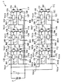
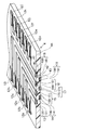
次に、インバータ装置用配線基板について図2〜図7を参照して説明する。図2は、インバータ装置用配線基板の断面を含む部分斜視図である。図3は、図2における電源配線パターン13の構成のみを示す斜視図である。図4は、図2における電源配線パターン14の構成のみを示す斜視図である。図5は、図2における電源配線パターン15の構成のみを示す斜視図である。図6は、図2における電源配線パターン13〜15の構成のみを示す斜視図である。図7は、図2における電源配線パターン16の一部の構成のみを示す斜視図である。なお、図2は、電源配線パターンのみを記載し、他の信号配線パターンは省略している。
Next, the wiring board for inverter devices will be described with reference to FIGS. FIG. 2 is a partial perspective view including a cross-section of the inverter device wiring board. FIG. 3 is a perspective view showing only the configuration of the power
図2に示すように、インバータ装置用配線基板4は、第1配線層40と、第2配線層41と、第3配線層42と、第4配線層43と、絶縁層44とから構成されている。第1〜第4配線層40〜43は、例えば銅からなり、例えば絶縁性を有する樹脂からなる絶縁層44を介して互いに所定間隔を隔てて積層されている。第1配線層40は、インバータ装置用配線基板4の上面に配設されている。第2配線層41は、第1配線層40の下方であって、インバータ装置用配線基板4の上面と平行な面に、絶縁層44を介して所定間隔を隔て隣接して配設されている。第3配線層42は、第2配線層41の下方であって、インバータ装置用配線基板4の上面と平行な面に、絶縁層44を介して所定間隔を隔て配設されている。第4配線層43は、第3配線層42の下方であって、インバータ装置用配線基板4の上面と平行な下面に、絶縁層44を介して所定間隔を隔て隣接して配設されている。
As shown in FIG. 2, the inverter device wiring board 4 includes a
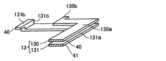
図2及び図3に示すように、電源配線パターン13(第1電源配線パターン)は、正極配線パターン130と、負極配線パターン131とから構成されている。正極配線パターン130は、第1配線層40に形成される略L字状の第1配線層パターン部130aと、第1配線層パターン部130aの端部に形成され、IGBT駆動用IC12aの電源端子に接続されるIC接続部130bとから構成されている。負極配線パターン131は、第2配線層41に形成される略L字状の第2配線層パターン部131aと、第1配線層40に形成され、IGBT駆動用IC12aの接地端子に接続されるIC接続部131bと、第2配線層パターン部131aとIC接続部131bとを接続する層間接続部131cとから構成されている。正極配線パターン130は、負極配線パターン131に対して積層方向に対向して配置されている。
As shown in FIGS. 2 and 3, the power supply wiring pattern 13 (first power supply wiring pattern) includes a positive
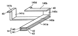
図2及び図4に示すように、 電源配線パターン14(第3電源配線パターン)は、正極配線パターン140と、負極配線パターン141とから構成されている。正極配線パターン140は、第3配線層42に形成されるI字状の第3配線層パターン部140aと、第1配線層40に形成され、第3配線層パターン部の長手方向に対して直交する方向に延びるI字状の第1配線層パターン部140bと、第3配線層パターン部140aと第1配線層パターン部140bとを接続する層間接続140c部と、第1配線層パターン部140bの端部に形成され、IGBT駆動用IC12bの電源端子に接続されるIC接続部140dとから構成されている。負極配線パターン141は、第4配線層43に形成される略L字状の第4配線層パターン部141aと、第1配線層40に形成され、IGBT駆動用IC12bの接地端子に接続されるIC接続部141bと、第4配線層パターン部141aとIC接続部141bとを接続する層間接続部141cとから構成されている。正極配線パターン140は、負極配線パターン141に対して積層方向に対向して配置されている。
As shown in FIGS. 2 and 4, the power supply wiring pattern 14 (third power supply wiring pattern) includes a positive
図2及び図5に示すように、電源配線パターン15(第2電源配線パターン)は、正極配線パターン150と、負極配線パターン151とから構成されている。正極配線パターン150は、第1配線層40に形成される略L字状の第1配線層パターン部150aと、第1配線層パターン部150aの端部に形成され、IGBT駆動用IC12cの電源端子に接続されるIC接続部150bとから構成されている。負極配線パターン151は、第2配線層41に形成される略L字状の第2配線層パターン部 151aと、第1配線層40に形成され、IGBT駆動用IC12cの接地端子に接続されるIC接続部151bと、第2配線層パターン部151aとIC接続部151bとを接続する層間接続部151cとから構成されている。正極配線パターン150は、負極配線パターン151に対して積層方向に対向して配置されている。
As shown in FIGS. 2 and 5, the power supply wiring pattern 15 (second power supply wiring pattern) includes a positive
図6に示すように、電源配線パターン14の第3配線層パターン部140a及び第4配線層パターン部141aが、電源配線パターン13、15の第1配線層パターン部130a、150a及び第2配線層パターン部131a、151aの間の領域に、積層方向に重ならないように配設されている。ここで、電源配線パターン13、14、15間の間隔は、絶縁性及び耐ノイズ性を確保することができる最適な寸法に設定されている。
As shown in FIG. 6, the third wiring
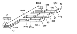
図2及び図7に示すように、電源配線パターン16は、正極配線パターン160と、負極配線パターン161とから構成されている。正極配線パターン160は、第1配線層40に形成される略櫛歯状の第1配線層パターン部160aと、第1配線層パターン部160aの端部に形成され、IGBT駆動用IC12d〜12fの電源端子にそれぞれ接続されるIC接続部160b〜160dとから構成されている。負極配線パターン161は、第2配線層41に形成される略櫛歯状の第2配線層パターン部161aと、第1配線層40に形成され、IGBT駆動用IC12d〜12fの接地端子にそれぞれ接続されるIC接続部161b〜161dと、第2配線層パターン部161aとIC接続部161b〜161dとを接続する層間接続部161e〜161gとから構成されている。正極配線パターン160は、負極配線パターン161に対して積層方向に対向して配置されている。なお、図7では省略されているが、図2に示すように、正極配線パターン160及び負極配線パターン161には、IGBT駆動用IC12j〜12lに接続される同様の略櫛歯状のパターンが、長手方向に延在するように設けられている。
As shown in FIGS. 2 and 7, the power
電源配線パターン17、19の構成は電源配線パターン14と、電源配線パターン18の構成は電源配線パターン13とほぼ同一である。そのため、詳細な説明は省略する。また、電源配線パターン15、17、18の配置関係は、電源配線パターン13〜15の配置関係と同一である。電源配線パターン18、19、16の配置関係も、電源配線パターン13〜15の配置関係と同一である。
The configurations of the power
最後に、効果について説明する。インバータ装置用配線基板4によれば、絶縁性及び耐ノイズ性を確保するとともに、インバータ装置1を小型化することができる。電源配線パターン14の第3配線層パターン部140a及び第4配線層パターン部141aは 、電源配線パターン13、15の第1配線層パターン部130a、150a及び第2配線層パターン部131a、151aの間の領域に、積層方向に重ならないように配設されている。そのため、電源配線パターン13〜15を同一配線層に形成した場合に比べ、インバータ装置用配線基板4を特殊な構造とすることなく、しかも面積を抑えた状態で、電源配線パターン13〜15間の距離を確保することができる。これにより、インバータ装置用配線基板4を大きくすることなく絶縁性を確保することができる。また、電源配線パターン13〜15間での重なりがなく、電源配線パターン13〜15を積層方向に重ねて配置した場合に比べ、容量を抑えることができる。これにより、容量結合に伴うノイズの侵入が抑えられ、耐ノイズ性を確保することができる。他の電源配線パターンについても同様である。従って、絶縁性及び耐ノイズ性を確保するとともに、インバータ装置を小型化することができる。
Finally, the effect will be described. According to the inverter device wiring board 4, insulation and noise resistance can be ensured, and the
また、電源配線パターン13〜16において、正極配線パターン130、140、150、160を、それぞれ負極配線パターン131、141、151、161に対して積層方向に対向して配置させることで、対応する正極配線パターン130、140、150、160と負極配線パターン131、141、151、161との間の容量が増加する。そのため、電圧が安定し、IGBT駆動用IC12a〜12fに安定的に電力を供給することができる。正極配線パターン130、140、150、160と、負極配線パターン131、141、151、161とを互いに隣接した配線層に配設することで、より容量が増加し、より安定的に電力を供給することができる。他の電源配線パターンについても同様である。
Further, in the power
さらに、インバータ装置用配線基板4を、車両に搭載され、車両を走行させるための駆動力を発生する2つの交流モータに電力を供給するインバータ装置1に用いることで、絶縁性及び耐ノイズ性の確保された小型の車載用インバータ装置を構成することができる。
Furthermore, by using the inverter device wiring board 4 for the
なお、本実施形態では、インバータ装置用配線基板4が、第1配線層40、第2配線層41、第3配線層42及び第4配線層43を有する4層構造の多層配線基板である例を挙げているが、これに限られるものではない。インバータ装置用配線基板は、5つ以上の配線層を有する多層配線基板であってもよい。これらの配線層のうち4つの配線層において同様の構成をとることができる。その場合においても同様の効果を得ることができる。
In the present embodiment, the inverter device wiring board 4 is a four-layer multilayer wiring board having the
1:インバータ装置、10a〜10l:IGBT、11a〜11l:フライホイールダイオード、12a〜12l:IGBT駆動用IC、13:電源配線パターン(第1電源配線パターン)、14:電源配線パターン(第3電源配線パターン)、15:電源配線パターン(第2電源配線パターン)、16〜19:電源配線パターン、130、140、150、160、170、180、190:正極配線パターン、131、141、151、161、171、181、191:負極配線パターン、130a、140b、150a:第1配線層パターン部、131a151a:第2配線層パターン部、140a:第3配線層パターン部、141a:第4配線層パターン部、130b、131b、140d、141b、150b、151b:IC接続部、131c、140c、141c、151c:層間接続部、2:直流電源、3:平滑用コンデンサ、4:インバータ装置用配線基板、40:第1配線層、41:第2配線層、42:第3配線層、43:第4配線層、44:絶縁層 1: inverter device, 10a to 10l: IGBT, 11a to 11l: flywheel diode, 12a to 12l: IGBT driving IC, 13: power supply wiring pattern (first power supply wiring pattern), 14: power supply wiring pattern (third power supply) Wiring pattern), 15: power wiring pattern (second power wiring pattern), 16-19: power wiring pattern, 130, 140, 150, 160, 170, 180, 190: positive wiring pattern, 131, 141, 151, 161 , 171, 181, 191: negative electrode wiring pattern, 130 a, 140 b, 150 a: first wiring layer pattern part, 131 a 151 a: second wiring layer pattern part, 140 a: third wiring layer pattern part, 141 a: fourth wiring layer pattern part , 130b, 131b, 140d, 141b, 150b, 151b: IC Connection part, 131c, 140c, 141c, 151c: interlayer connection part, 2: DC power supply, 3: smoothing capacitor, 4: inverter device wiring board, 40: first wiring layer, 41: second wiring layer, 42: Third wiring layer, 43: fourth wiring layer, 44: insulating layer
Claims (6)
該第1電源配線パターンは、該第1配線層又は該第2配線層のいずれか一方に該正極配線パターンの少なくとも一部が、他方に該負極配線パターンの少なくとも一部がそれぞれ形成され、
該第2電源配線パターンは、該第1電源配線パターンと所定間隔を隔て該第1配線層又は該第2配線層のいずれか一方に該正極配線パターンの少なくとも一部が、他方に該負極配線パターンの少なくとも一部がそれぞれ形成され、
該第3電源配線パターンは、該第1電源配線パターンと該第2電源配線パターンの間の領域であって、該第3配線層又は該第4配線層のいずれか一方に該正極配線パターンの少なくとも一部が、他方に該負極配線パターンの少なくとも一部がそれぞれ形成されていることを特徴とするインバータ装置用配線基板。 The first wiring layer includes a first wiring layer, a second wiring layer, a third wiring layer, and a fourth wiring layer, each of which is laminated with a predetermined interval therebetween via an insulating layer. Power is supplied independently to the switching element drive circuit provided for each switching element of the inverter device formed in at least one of the layer, the second wiring layer, the third wiring layer, and the fourth wiring layer. In a wiring board for an inverter device comprising a first power wiring pattern, a second power wiring pattern, and a third power wiring pattern, each comprising a positive wiring pattern and a negative wiring pattern,
In the first power supply wiring pattern, at least a part of the positive electrode wiring pattern is formed on either the first wiring layer or the second wiring layer, and at least a part of the negative electrode wiring pattern is formed on the other.
The second power supply wiring pattern has at least a part of the positive electrode wiring pattern on one side of the first wiring layer or the second wiring layer and a negative wiring on the other side with a predetermined distance from the first power supply wiring pattern. At least part of the pattern is formed,
The third power supply wiring pattern is a region between the first power supply wiring pattern and the second power supply wiring pattern, and the positive power supply wiring pattern is formed on either the third wiring layer or the fourth wiring layer. A wiring board for an inverter device, wherein at least a part of the negative electrode wiring pattern is formed at least on the other side.
前記第3配線層及び前記第4配線層は、前記第1配線層及び前記第2配線層から所定間隔を隔て積層方向に互いに隣接して配設されていることを特徴とする請求項1〜3のいずれかに記載のインバータ装置用配線基板。 The first wiring layer and the second wiring layer are disposed adjacent to each other in the stacking direction,
The third wiring layer and the fourth wiring layer are disposed adjacent to each other in the stacking direction at a predetermined interval from the first wiring layer and the second wiring layer. 4. The wiring board for an inverter device according to any one of 3 above.
前記第2電源配線パターンは、前記第1配線層に前記正極配線パターンの少なくとも一部が、前記第2配線層に前記負極配線パターンの少なくとも一部がそれぞれ形成され、
前記第3電源配線パターンは、前記第3配線層に前記正極配線パターンの少なくとも一部が、前記第4配線層に前記負極配線パターンの少なくとも一部がそれぞれ形成されていることを特徴とする請求項1〜4のいずれかに記載のインバータ装置用配線基板。 In the first power supply wiring pattern, at least a part of the positive electrode wiring pattern is formed in the first wiring layer, and at least a part of the negative electrode wiring pattern is formed in the second wiring layer, respectively.
In the second power supply wiring pattern, at least a part of the positive electrode wiring pattern is formed in the first wiring layer, and at least a part of the negative electrode wiring pattern is formed in the second wiring layer, respectively.
The third power supply wiring pattern is characterized in that at least a part of the positive electrode wiring pattern is formed on the third wiring layer, and at least a part of the negative electrode wiring pattern is formed on the fourth wiring layer. Item 5. The wiring board for an inverter device according to any one of Items 1 to 4.
Priority Applications (1)
| Application Number | Priority Date | Filing Date | Title |
|---|---|---|---|
| JP2006004803A JP4333675B2 (en) | 2006-01-12 | 2006-01-12 | Inverter wiring board |
Applications Claiming Priority (1)
| Application Number | Priority Date | Filing Date | Title |
|---|---|---|---|
| JP2006004803A JP4333675B2 (en) | 2006-01-12 | 2006-01-12 | Inverter wiring board |
Publications (2)
| Publication Number | Publication Date |
|---|---|
| JP2007189801A JP2007189801A (en) | 2007-07-26 |
| JP4333675B2 true JP4333675B2 (en) | 2009-09-16 |
Family
ID=38344589
Family Applications (1)
| Application Number | Title | Priority Date | Filing Date |
|---|---|---|---|
| JP2006004803A Active JP4333675B2 (en) | 2006-01-12 | 2006-01-12 | Inverter wiring board |
Country Status (1)
| Country | Link |
|---|---|
| JP (1) | JP4333675B2 (en) |
Cited By (4)
| Publication number | Priority date | Publication date | Assignee | Title |
|---|---|---|---|---|
| CN103069358A (en) * | 2010-06-07 | 2013-04-24 | 杰森·A·苏利万 | Miniturization techniques, systems, and apparatus relating to power supplies, memory, interconnections, and leds |
| US9606577B2 (en) | 2002-10-22 | 2017-03-28 | Atd Ventures Llc | Systems and methods for providing a dynamically modular processing unit |
| US9961788B2 (en) | 2002-10-22 | 2018-05-01 | Atd Ventures, Llc | Non-peripherals processing control module having improved heat dissipating properties |
| US10285293B2 (en) | 2002-10-22 | 2019-05-07 | Atd Ventures, Llc | Systems and methods for providing a robust computer processing unit |
Families Citing this family (4)
| Publication number | Priority date | Publication date | Assignee | Title |
|---|---|---|---|---|
| JP5029900B2 (en) | 2007-11-20 | 2012-09-19 | アイシン・エィ・ダブリュ株式会社 | Motor control device |
| JP5444619B2 (en) * | 2008-02-07 | 2014-03-19 | 株式会社ジェイテクト | Multi-layer circuit board and motor drive circuit board |
| JP4644275B2 (en) * | 2008-07-29 | 2011-03-02 | 日立オートモティブシステムズ株式会社 | Power converter and electric vehicle |
| DE102017221787A1 (en) * | 2017-12-04 | 2019-06-06 | Zf Friedrichshafen Ag | Printed circuit board for converting an input phase into at least one output phase and a DC motor with such a printed circuit board |
-
2006
- 2006-01-12 JP JP2006004803A patent/JP4333675B2/en active Active
Cited By (6)
| Publication number | Priority date | Publication date | Assignee | Title |
|---|---|---|---|---|
| US9606577B2 (en) | 2002-10-22 | 2017-03-28 | Atd Ventures Llc | Systems and methods for providing a dynamically modular processing unit |
| US9961788B2 (en) | 2002-10-22 | 2018-05-01 | Atd Ventures, Llc | Non-peripherals processing control module having improved heat dissipating properties |
| US10285293B2 (en) | 2002-10-22 | 2019-05-07 | Atd Ventures, Llc | Systems and methods for providing a robust computer processing unit |
| US10849245B2 (en) | 2002-10-22 | 2020-11-24 | Atd Ventures, Llc | Systems and methods for providing a robust computer processing unit |
| US11751350B2 (en) | 2002-10-22 | 2023-09-05 | Atd Ventures, Llc | Systems and methods for providing a robust computer processing unit |
| CN103069358A (en) * | 2010-06-07 | 2013-04-24 | 杰森·A·苏利万 | Miniturization techniques, systems, and apparatus relating to power supplies, memory, interconnections, and leds |
Also Published As
| Publication number | Publication date |
|---|---|
| JP2007189801A (en) | 2007-07-26 |
Similar Documents
| Publication | Publication Date | Title |
|---|---|---|
| JP4333675B2 (en) | Inverter wiring board | |
| JP6237554B2 (en) | Power conversion device control board | |
| EP2264894A1 (en) | Power module with additional transient current path and power module system | |
| US20140111959A1 (en) | Laminated busbar for power converter and the converter thereof | |
| JP6288769B2 (en) | Semiconductor power module, power conversion device, and moving body using the same | |
| JP6020572B2 (en) | Power converter | |
| JP7070149B2 (en) | Switching circuit | |
| JP6184507B2 (en) | Driver board and power conversion device | |
| JP2016046842A (en) | Power conversion device and elevator employing the same | |
| JP5475722B2 (en) | Power converter | |
| JP6365362B2 (en) | Control board for power converter | |
| JP2014222962A (en) | Power conversion device | |
| JP2017017881A (en) | Power converter | |
| JP2013192403A (en) | Power supply device | |
| US10381947B2 (en) | Power conversion apparatus | |
| CN107800304B (en) | Power conversion device | |
| JP5994462B2 (en) | Inverter device | |
| JP4828170B2 (en) | Power converter | |
| KR101887266B1 (en) | Busplate having function of reducing a stray inductance and power stack comprising the same | |
| JP7471504B2 (en) | Inverter Device | |
| CN215580947U (en) | Inverter device | |
| CN216122227U (en) | Motor drive system | |
| JP6440511B2 (en) | Rotating machine drive | |
| US10658925B2 (en) | Circuit board to transform an entry phase in at least one output phase and direct-current-motor with such circuit board | |
| JP6229148B2 (en) | Inverter device and motor drive device |
Legal Events
| Date | Code | Title | Description |
|---|---|---|---|
| A621 | Written request for application examination |
Free format text: JAPANESE INTERMEDIATE CODE: A621 Effective date: 20080313 |
|
| A977 | Report on retrieval |
Free format text: JAPANESE INTERMEDIATE CODE: A971007 Effective date: 20090528 |
|
| TRDD | Decision of grant or rejection written | ||
| A01 | Written decision to grant a patent or to grant a registration (utility model) |
Free format text: JAPANESE INTERMEDIATE CODE: A01 Effective date: 20090602 |
|
| A01 | Written decision to grant a patent or to grant a registration (utility model) |
Free format text: JAPANESE INTERMEDIATE CODE: A01 |
|
| A61 | First payment of annual fees (during grant procedure) |
Free format text: JAPANESE INTERMEDIATE CODE: A61 Effective date: 20090615 |
|
| FPAY | Renewal fee payment (event date is renewal date of database) |
Free format text: PAYMENT UNTIL: 20120703 Year of fee payment: 3 |
|
| R150 | Certificate of patent or registration of utility model |
Ref document number: 4333675 Country of ref document: JP Free format text: JAPANESE INTERMEDIATE CODE: R150 Free format text: JAPANESE INTERMEDIATE CODE: R150 |
|
| FPAY | Renewal fee payment (event date is renewal date of database) |
Free format text: PAYMENT UNTIL: 20120703 Year of fee payment: 3 |
|
| FPAY | Renewal fee payment (event date is renewal date of database) |
Free format text: PAYMENT UNTIL: 20130703 Year of fee payment: 4 |
|
| R250 | Receipt of annual fees |
Free format text: JAPANESE INTERMEDIATE CODE: R250 |
|
| R250 | Receipt of annual fees |
Free format text: JAPANESE INTERMEDIATE CODE: R250 |
|
| R250 | Receipt of annual fees |
Free format text: JAPANESE INTERMEDIATE CODE: R250 |
|
| R250 | Receipt of annual fees |
Free format text: JAPANESE INTERMEDIATE CODE: R250 |
|
| R250 | Receipt of annual fees |
Free format text: JAPANESE INTERMEDIATE CODE: R250 |
|
| R250 | Receipt of annual fees |
Free format text: JAPANESE INTERMEDIATE CODE: R250 |
|
| R250 | Receipt of annual fees |
Free format text: JAPANESE INTERMEDIATE CODE: R250 |
|
| R250 | Receipt of annual fees |
Free format text: JAPANESE INTERMEDIATE CODE: R250 |
|
| R250 | Receipt of annual fees |
Free format text: JAPANESE INTERMEDIATE CODE: R250 |
|
| R250 | Receipt of annual fees |
Free format text: JAPANESE INTERMEDIATE CODE: R250 |