EP2157604A1 - Widerstandselement, neuronenelement und vorrichtung zur verarbeitung von informationen über neuronale netzwerke - Google Patents
Widerstandselement, neuronenelement und vorrichtung zur verarbeitung von informationen über neuronale netzwerke Download PDFInfo
- Publication number
- EP2157604A1 EP2157604A1 EP08764748A EP08764748A EP2157604A1 EP 2157604 A1 EP2157604 A1 EP 2157604A1 EP 08764748 A EP08764748 A EP 08764748A EP 08764748 A EP08764748 A EP 08764748A EP 2157604 A1 EP2157604 A1 EP 2157604A1
- Authority
- EP
- European Patent Office
- Prior art keywords
- resistive element
- neuron
- input
- molecule
- neural network
- Prior art date
- Legal status (The legal status is an assumption and is not a legal conclusion. Google has not performed a legal analysis and makes no representation as to the accuracy of the status listed.)
- Withdrawn
Links
Images





Classifications
-
- G—PHYSICS
- G06—COMPUTING OR CALCULATING; COUNTING
- G06N—COMPUTING ARRANGEMENTS BASED ON SPECIFIC COMPUTATIONAL MODELS
- G06N3/00—Computing arrangements based on biological models
- G06N3/002—Biomolecular computers, i.e. using biomolecules, proteins, cells
-
- B—PERFORMING OPERATIONS; TRANSPORTING
- B82—NANOTECHNOLOGY
- B82Y—SPECIFIC USES OR APPLICATIONS OF NANOSTRUCTURES; MEASUREMENT OR ANALYSIS OF NANOSTRUCTURES; MANUFACTURE OR TREATMENT OF NANOSTRUCTURES
- B82Y10/00—Nanotechnology for information processing, storage or transmission, e.g. quantum computing or single electron logic
-
- G—PHYSICS
- G06—COMPUTING OR CALCULATING; COUNTING
- G06N—COMPUTING ARRANGEMENTS BASED ON SPECIFIC COMPUTATIONAL MODELS
- G06N3/00—Computing arrangements based on biological models
- G06N3/02—Neural networks
- G06N3/06—Physical realisation, i.e. hardware implementation of neural networks, neurons or parts of neurons
- G06N3/063—Physical realisation, i.e. hardware implementation of neural networks, neurons or parts of neurons using electronic means
-
- H—ELECTRICITY
- H01—ELECTRIC ELEMENTS
- H01C—RESISTORS
- H01C17/00—Apparatus or processes specially adapted for manufacturing resistors
- H01C17/06—Apparatus or processes specially adapted for manufacturing resistors adapted for coating resistive material on a base
- H01C17/065—Apparatus or processes specially adapted for manufacturing resistors adapted for coating resistive material on a base by thick film techniques, e.g. serigraphy
- H01C17/06506—Precursor compositions therefor, e.g. pastes, inks, glass frits or green body
- H01C17/06573—Precursor compositions therefor, e.g. pastes, inks, glass frits or green body characterised by the permanent binder
- H01C17/06586—Precursor compositions therefor, e.g. pastes, inks, glass frits or green body characterised by the permanent binder composed of organic material
-
- H—ELECTRICITY
- H01—ELECTRIC ELEMENTS
- H01C—RESISTORS
- H01C7/00—Non-adjustable resistors formed as one or more layers or coatings; Non-adjustable resistors made from powdered conducting material or powdered semi-conducting material with or without insulating material
- H01C7/006—Thin film resistors
-
- H—ELECTRICITY
- H10—SEMICONDUCTOR DEVICES; ELECTRIC SOLID-STATE DEVICES NOT OTHERWISE PROVIDED FOR
- H10K—ORGANIC ELECTRIC SOLID-STATE DEVICES
- H10K10/00—Organic devices specially adapted for rectifying, amplifying, oscillating or switching; Organic capacitors or resistors having potential barriers
- H10K10/50—Bistable switching devices
Definitions
- the present invention relates to a resistive element, a neuron element including the resistive element in an input part, and a neural network information processing device employing the neuron element, and specifically relates to hysteresis exhibited by the resistive element.
- the scanning tunneling microscope has been invented in the late 1980s, and thus not only observation of atoms and molecules but also operation of atoms and molecules on a one-by-one basis has become possible. For example, an example in which atoms are arranged on a surface of a crystal to write a character has been reported.
- the width of an electrically-conductive molecule is only 0.5 nm.
- This molecular wire material can realize an interconnect having high density that is higher by a factor of several thousand compared with a line width of about 100 nm, which is realized in the present integrated circuit technique.
- recording density higher than that of the DVD by a factor of ten thousand or larger is possible.
- connection part between the constituent molecules and the electrode has high electric resistance and this high resistance restricts the characteristics of the molecular device.
- an organic field effect transistor carrier movement in organic molecules in the channel region is modulated by change in an electric field acting on the organic molecules.
- the contact resistance across the interface between the constituent molecules and the electrode is very high and this contact resistance intensely affects the operating characteristics of the transistor.
- one of the present inventors has proposed a functional molecular element based on a new principle in Japanese Patent Laid-Open No. 2004-221553 .
- This molecular element functions as a molecular switch that changes the molecular structure based on the effect of an electric field and turns ON and OFF a current. Also in this molecular element, if the contact resistance across the interface between the constituent molecules and the electrode is high, this contact resistance affects the operating characteristics of the molecular element.
- one of the present inventors has proposed a functional molecular element having a novel structure that allows decrease in the contact resistance across the interface between the constituent molecules and the electrode, a method for manufacturing the same, and a functional molecular device in Japanese Patent Laid-Open No. 2006-351623 (pp. 11 to 15, FIGS. 1 to 5 ).
- This functional molecular element is e.g. a functional molecular element in which a n-conjugated molecule in which a side chain part is coupled to a backbone part having a planar or substantially-planar structure formed of a n-conjugated system is absorbed by an electrode at the side chain part, to thereby form an absorbed molecule that is so disposed that the planar or substantially-planar structure of the backbone part is in substantially parallel to the electrode, and a structural body composed of at least the absorbed molecule and the electrode has a function to allow a current to flow in a direction intersecting with the planar or substantially-planar structure.
- the von Neumann computer has achieved great development based on the semiconductor technique of fabricating a micro semiconductor chip on a semiconductor wafer by lithography, etching, and so on.
- the von Neumann computer is no good, such as pattern recognition.
- the neuro-computer imitating the creature's brain is attracting attention.
- the creature's brain is formed with complicated coupling of a large number of nerve cells (neurons) in a network manner ("Nou no Keisan Riron,” Mitsuo Kawato, Sangyo Tosho, 1996).
- FIG. 7 is a schematic explanatory diagram showing the configuration of a nerve cell 100.
- the nerve cell 100 is composed of a cell body 101, dendrites 102, an axon 103, nerve terminals 104, synapses 105, and so on.
- the cell body 101 includes a nucleus 101a and so on and is the main body part of the nerve cell 100.
- the dendrites 102 have a structure like a large number of branches extending from the cell body 101 and are parts equivalent to input terminals of the nerve cell 100.
- the axon 103 has a structure with a shape of one long, thick funiculus extending from the cell body 101 and is the part that generates the output of the nerve cell 100.
- the tip thereof is branched into plural paths to form the nerve terminals 104 that send signals to other output-side nerve cells 109.
- the synapse 105 is a coupling part that interconnects a nerve cell and a nerve cell.
- Input signals 107 from other input-side nerve cells 106 are transmitted to the nerve cell 100 via input-side synapses 105a between the nerve terminals of the input-side nerve cells 106 and the dendrites 102 and the cell body 101 of the nerve cell 100.
- output signals 108 from the axon 103 of the nerve cell 100 are transmitted to the output-side nerve cells 109 via output-side synapses 105b between the nerve terminals 104 and the dendrites and the cell bodies of the nerve cells 109.
- one nerve cell 100 can receive the input signals 107 from the input-side nerve cells 106 via several thousand or more synapses 105a.
- the nerve cell 100 executes information processing for this large number of input signals 107 and outputs the result to a large number of output-side nerve cells 109 from one axon 103.
- the signal transmission between nerve cells via the synapses 105 is carried out based on potential change.
- the operation of the nerve cells at the time will be described below by taking excitation generation as an example.
- the membrane potential of the cell membrane of the axon 103 is generally kept at a negative potential (resting potential) of about -60 mV.
- the membrane potential of the axon 103 rises up. The potential rises due to the respective input signals 107 are added to each other.
- the axon 103 If the sum of the potential rises due to a large number of input signals 107 surpasses the threshold (potential higher than the resting potential by about 15 mV), the axon 103 generates the output signal 108 with a height of about 115 mV and a duration of about 0.5 ms at that moment.
- the output signal 108 is sent from the nerve terminals 104 to the output-side nerve cells 109 via the synapses 105b.
- the signal transmission between nerve cells is carried out by a pulse voltage having a substantially-constant waveform, and the number of pulses per unit time is large when the brain activity is strong.
- the signal transmission is necessarily carried out via the synapses 105.
- the cell body of the output-side nerve cell 109 receives not the output signal 108 itself but a pulse resulting from the change by the synapse 105b as a signal. Therefore, depending on the difference in the signal transmission characteristic of the synapse 105b, the differences of the following (1) to (4) arise in the effect of the output signal 108 in the output-side nerve cell 109.
- the relationship between nerve cells depends on whether or not the synapse coupling is present and the signal transmission characteristic of the synapse.
- one nerve cell has only a simple function, the human brain includes ten billion or more nerve cells. A large number of cells of these nerve cells simultaneously operate in parallel to execute distributed processing, which allows exertion of high information processing ability. Furthermore, a learning effect is exerted by formation of synapse coupling and change in the signal transmission characteristic of the synapse.
- a neural network is an information processing circuit network imitating the above-described characteristics of the information processing in the brain, and is formed of neuron elements imitating nerve cells (neurons) ( Neural Net no Kiso to Ouyou, Norio Baba, Fumio Kojima, Seiichi Ozawa, Kyoritsu Shuppan Co., Ltd. (1994 ), Jissen Neural Net, Takeo Miyazawa, monthly ASCII, Vol. 12, the September 1988 issue, p. 237 to Vol. 13, the April 1989 issue, p. 341 ).
- the neuro-computer is a computer that is formed of the neural network and characterized in parallel distributed processing.
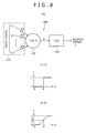
- FIG. 8(a) is a schematic explanatory diagram showing the functions of the neuron element in a model manner.
- a neuron element 200 is composed of an input part 210, an addition part 220, and an output part 230.
- the input part 210 corresponds to the function of the synapse 105.
- the connection weight wi corresponds to the signal transmission characteristic of the synapse 105.
- the addition part 220 corresponds to the function of the cell body 101.
- X w ⁇ 1 ⁇ x ⁇ 1 + w ⁇ 2 ⁇ x ⁇ 2 + ⁇ + wnxn
- the total sum (net value) X corresponds to the rise of the axon potential due to the input signals.
- the input-side neuron element giving the input signal xi has larger influence on the neuron element 200 when the connection weight wi is set larger. Furthermore, it can be expressed that the neuron element giving the input signal xi has no effective influence on the neuron element 200 when the connection weight wi is set to zero, and it can be expressed that the neuron element giving the input signal xi has inhibitory influence on the neuron element 200 when the connection weight wi is set negative.
- the output part 230 defines an output signal Y(X) as a function of the total sum (net value) X and outputs it.
- FIG. 8 (b-1) shows an example in which the output function Y(X) is a threshold type function (step function) including ⁇ as the threshold. This is the function employed when McCulloch and Pitts modeled the operation of the nerve cell first time and defined the formal neuron as a multi-input one-output function.
- FIG. 8 (b-2) shows an example in which the output function Y(X) is a sigmoid function represented by the following equation.
- Y 1 / 1 + exp - aX
- the sigmoid function is a function that has a nonlinear characteristic with respect to the input X but monotonically increases from zero to one in linkage with increase in X.
- Symbol a in the equation is a parameter that determines the steepness of the slope of the function, and larger a brings the function Y closer to a step function.
- the threshold ⁇ can be introduced in the sigmoid function.
- Y 1 / 1 + exp - a ⁇ X - ⁇
- a neural network can be formed by connecting a large number of neuron elements 200.
- the structure and characteristics of the network depend on the way of the connection of the neuron elements.
- the neural network is roughly categorized into a hierarchical network and an interconnected network, depending on the network structure.
- FIG. 9(a) is an explanatory diagram showing one example of the hierarchical neural network.
- This example is an example in which a hierarchical neural network 300 is composed of three layers of an input layer 310, an intermediate layer 320, and an output layer 330. Input signals are applied to neuron elements 301 in the input layer 310, and output signals in response to the input signals are brought out from the neuron elements 301 in the output layer 330.
- the hierarchical neural network is formed by disposing the neuron elements 301 in plural layers and the neuron elements 301 are coupled to each other between the layers, and the signals are transmitted from layer to layer in only one direction from the input layer 310 toward the output layer 330.
- the hierarchical neural network achievement of a more preferred output signal is permitted by changing the connection weights wi of the respective neuron elements and the threshold ⁇ of the output function based on the error between an actual output signal in response to a certain input signal and the desired output signal.
- This is a learning function possessed by the hierarchical neural network. Because the hierarchical neural network has such a learning function, it is effectively applied to pattern recognition by PDP (Parallel Distributed Processing), such as image recognition, character recognition, and audio recognition, at which the von Neumann computer is no good, and various fields in which autonomous learning is required.
- PDP Parallel Distributed Processing
- FIG. 9(b) is an explanatory diagram showing a Hopfield network as one example of the interconnected neural network.
- a Hopfield network 400 all of neuron elements 401 are coupled to each other to form one layer. Therefore, the direction of the signal flow is not one direction, but feedback of the signal to each other is carried out.
- the connection weight wij is the connection weight for the input to the i-th neuron element 401 from the j-th neuron element 401 (in FIG. 9(b) , the numeral in the rectangle indicating a connection weight wij 402 is ij as the combination of i and j).
- the Hopfield network is applied to the field of associative memory and a field in which an analogous approximate solution is obtained for a combinatorial optimization problem such as the traveling salesman problem, inverse matrix calculation, or the like, which involves many variables and is impossible for the von Neumann computer to calculate.
- the von Neumann computer In studies on the neural network, the von Neumann computer is used as hardware and simulation of the operation thereof is performed by software in many cases. However, with this configuration, high-speed performance of the neural network as a parallel analog network can not be really utilized. Therefore, to put a neural network information processing device into practical use, it is required to employ electronic circuits as the respective parts of the neuron element 200.
- an element obtained by coupling neuron elements to each other via an EEPROM (Electrically Erasable Programmable Read-Only Memory), which is a nonvolatile memory, has been proposed as a neuron element in Japanese Patent Laid-Open No. Hei 3-144785 (pp. 2 to 4, FIGS. 1 to 3 ).
- the respective input signals to the neurons are multiplied by coefficients that are held by the amount of charge accumulated in the trap of the EEPROM or the amount of charge accumulated in the floating gate and correspond to the weights that should be each given to a respective one of the signals.
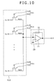
- FIG. 10 is an explanatory diagram showing one example of the configuration of an input part and an addition part in a conventional neuron element.
- input circuits 511 equivalent to synapses are provided in an input part 510.
- the connection weight wi corresponds to the signal transmission characteristic of the synapse.
- a gate voltage corresponding to the connection weight wi is applied to a gate electrode 513 of the transistor 512 by the operation of a memory circuit, whose diagrammatic representation is omitted.
- the electrical conductivity of the transistor 512 is controlled by the gate voltage, so that a current signal equivalent to the weighted signal wixi is sent from the drain electrode of the transistor 512 to an addition part 20.
- the addition part 20 is a current-voltage conversion circuit formed of an OP amp (operational amplifier) 21.
- the output currents from the respective input circuits 511 in the input part 510 are collected into the inverting input terminal of the OP amp 21 and flow from a feedback resistor 22.
- a voltage signal corresponding to the total sum (net value) X defined by the following equation is output to an output circuit 30.
- X w ⁇ 1 ⁇ x ⁇ 1 + w ⁇ 2 ⁇ x ⁇ 2 + ⁇ + wnxn
- the gate voltage corresponding to the connection weight wi needs to be held, and therefore the memory circuit, voltage generation means, and so on, whose diagrammatic representation is omitted, are necessary.
- a large number of neuron elements need to be integrated for forming a neural network. Considering that a much larger number of connection weights than the neuron elements are included in the neuron elements, the configuration of the above-described neuron element is impractical.
- the creature's brain has such a learning function that, if a signal passes through the same synapse many times, the characteristics of the synapse are so gradually changed that the synapse comes to allow the passage of the signal therethrough more easily.
- the EEPROM is a memory element that stores the peak voltage, and the memory thereof does not change even when a voltage with the same magnitude is repeatedly applied thereto. That is, the EEPROM does not have the function to store "repetition.” Therefore, the memory element that stores the peak voltage, such as the EEPROM, can not realize the learning function possessed by the creature's brain.
- the present invention is made in view of these circumstances, and an object thereof is to provide a resistive element having unique electrical conductivity, a neuron element that includes an input part formed of a simple circuit and has excellent learning ability, and a neural network information processing device employing the neuron element.
- the present invention relates to a first resistive element that exhibits hysteresis in which the resistance of a resistor decreases if a voltage is applied to both sides of the resistor to make a current pass through the resistor, and relates to a second resistive element in which the resistance of a resistor gradually increases if voltage application to both sides of the resistor is kept absent.
- the present invention relates to a first neuron element that is a neuron element having an input part that receives a plurality of input signals and, in response to the input signals, creates weighted signals as the products of the input signals and connection weights corresponding to the input signals, an addition part that obtains the total sum of the plurality of weighted signals, and an output part that outputs an output signal as a function of the total sum, and being characterized in that the first resistive element is used as an element that creates the weighted signal from the input signal in the input part, and the resistance of the resistive element decreases due to a current flowing through the resistive element in reception of the input signal, and as a result a current flowing through the resistive element in reception of a subsequent input signal comes to flow more easily, and thereby a learning effect is obtained.
- the present invention relates to a second neuron element that is characterized in that the second resistive element is used as an element that creates the weighted signal from the input signal in the input part, and the resistance of the resistive element gradually increases if reception of the input signal is absent.
- the present invention relates to a neural network information processing device formed by connecting a plurality of the first or second neuron elements.
- the first resistive element of the present invention is a unique resistive element that exhibits hysteresis in which the resistance of a resistor decreases if a voltage is applied to both sides of the resistor to make a current pass through the resistor.
- the second resistive element is a unique resistive element in which the resistance of a resistor gradually increases if voltage application to both sides of the resistor is kept absent.
- the hysteresis exhibited by the first resistive element can be compared to history recording. Furthermore, if the phenomenon exhibited by the second resistive element is combined with the hysteresis, it is equivalent to erasing (forgetting) of the history recording.
- the first resistive element and the second resistive element are the first elements that can record the history such as repetition.
- the first resistive element is used as an element that creates the weighted signal from the input signal in the input part. Therefore, the resistance of the resistive element decreases due to a current flowing through the resistive element in reception of the input signal, and as a result a current flowing through the resistive element in reception of a subsequent input signal comes to flow more easily, and thereby a learning effect is obtained. Furthermore, in the second neuron element of the present invention, the second resistive element is used as an element that creates the weighted signal from the input signal in the input part. Therefore, the resistance of the resistive element gradually increases if reception of the input signal is absent.
- the first resistive element and the second resistive element are neuron elements that can realize the learning function possessed by the creature's brain, "the more the brain is used, the wiser the brain becomes," with a simple configuration. Furthermore, if these neuron elements are used, an autonomous learning function can be automatically given to an interconnected neural network such as a Hopfield network.
- the neural network information processing device of the present invention is formed by connecting a plurality of the above-described neuron elements of the present invention, and thus can exert excellent learning ability with a simple configuration.
- the resistance of the resistor gradually increase toward a resistance value possessed before current application if voltage application is stopped and current passage is kept absent.
- this phenomenon is equivalent to erasing (forgetting) of the history recording.
- the learning function similar to that of the creature's brain is exerted. It is not that the gradual erasing of the history recording involves no disadvantageous aspect.
- a memory element can be used in combination only for this part.
- the resistor be a functional molecular element composed of an organic functional molecule. Because there are an extremely wide variety of organic functional molecules, a proper functional molecule can be easily found.
- opposed electrodes obtained by disposing a plurality of electrodes opposed to each other be formed, and a ⁇ -conjugated molecule in which a side chain part is coupled to a backbone part having a substantially-planar structure formed of a ⁇ -conjugated system be absorbed by the electrode at the side chain part, and thereby an absorbed molecule that is so disposed that the substantially-planar structure of the backbone part is in substantially parallel to the opposed electrodes be formed for each of the opposed electrodes, and a structural body composed of at least the absorbed molecule and the opposed electrodes have a function to allow a current to flow in a direction intersecting with the substantially-planar structure depending on a voltage applied between the opposed electrodes.
- the contact resistance between the functional molecule and the electrode is high, and as a result the element performance is frequently restricted.
- the ⁇ -conjugated molecule is formed with coupling of a side chain part to a backbone part having a substantially-planar structure formed of a ⁇ -conjugated system.
- the substantially-planar structure of the backbone part is disposed in substantially parallel to the electrode due to absorption of the side chain part by the electrode, and the absorbed molecule can assume a structure in tight contact with the electrode.
- the electrical interaction between the ⁇ -electrons forming the ⁇ -conjugated system and the electrode becomes favorable, and the contact resistance between the ⁇ -conjugated molecule and the electrode is suppressed to low resistance.
- the functional molecular element is a functional molecule element in which a structural body composed of at least the absorbed molecule and the opposed electrodes have a function to allow a current to flow in a direction intersecting with the substantially-planar structure depending on a bias voltage applied between the opposed electrodes.
- the contact resistance at the opposed electrodes is suppressed to low resistance as described above, and the influence thereof is small.
- the current-voltage characteristic of the functional molecular element depends mainly on the electrical characteristic of an assembly of the absorbed molecule, the ⁇ -conjugated molecule, and so on, existing between the opposed electrodes.
- an array structural body arising from stacking of the same kind of ⁇ -conjugated molecules as the absorbed molecule or/and another kind of ⁇ -conjugated molecules along one direction over the backbone part of the absorbed molecule by intermolecular ⁇ - ⁇ stacking at the backbone part be formed as a part of the structural body between the opposed electrodes, and the structural body have a function to allow a current to flow in the stacking direction of the array structural body. If the array structural body is formed by the intermolecular ⁇ - ⁇ stacking as described above, a current can be made to effectively flow in the stacking direction of the array structural body due to the interaction between ⁇ -electrodes.
- the side chain part of the ⁇ -conjugated molecule have a flexible structure in the functional molecule. If this is employed, the side chain part comes to be absorbed on the electrode more easily, and the resistance between the ⁇ -conjugated molecule and the electrode can be decreased. It is preferable that the side chain part be formed of an alkyl group, an alkoxy group, a silanyl group, or an aromatic ring to which an alkyl group, an alkoxy group, or a silanyl group is coupled.
- the ⁇ -conjugated molecule and/or another kind of ⁇ -conjugated molecule be a complex of a central metal ion and a linear tetrapyrrole derivative in the functional molecule.
- the array structural body composed of a complex including a zinc ion as the central metal ion exhibits the ON and OFF switching characteristic with favorable electric conductivity based on the presence and absence of an electric field acting thereon.
- a transistor and so on can be fabricated.
- the central metal ion besides the zinc ion, a metal ion of a transition element or a typical element, such as a copper ion or a nickel ion, can be used.
- At least the ⁇ -conjugated molecule be a biladienone derivative represented by General formula (1).
- General formula (1) (in General formula (1), R 1 , R 2 , R 3 , and R 4 are the same or different alkyl groups that are independent of each other and each have a carbon number of 3 to 12.)
- R 1 , R 2 , R 3 , and R 4 may be any as long as the number of carbon atoms is 3 to 12.
- -C 10 H 21 and -C 12 H 25 are cited.
- the ⁇ -conjugated molecule is fixed in such a state as to be favorably aligned on the electrode without being crystallized.
- synthesis is also easy.
- the number of carbon atoms is one or two, the ⁇ -conjugated molecule is easily crystallized, and comes not to exhibit liquid-crystal-like properties and to cause an alignment defect easily.
- the number of carbon atoms is 13 or larger, the alignment is difficult on the contrary, and synthesis is also difficult.
- the resistance of the resistive element gradually increase toward a resistance value possessed before the learning effect is obtained and the learning effect be gradually lost. As described above, this is equivalent to the disappearance of the learning effect.
- the learning effect is accumulated if it is necessary, and the learning effect is lost if it becomes unnecessary.
- the learning function similar to that of the creature's brain is exerted. If long-term, stable holding of the learning effect is necessary, a memory element can be used in combination only for this part.
- the neural network information processing device of the present invention be formed as a hierarchical neural network information processing device in which the neuron elements are disposed in a plurality of layers and the neuron elements are coupled to each other between the layers.
- it is preferable that it be formed as an interconnected neural network information processing device in which all of the neuron elements are coupled to each other to form one layer.
- Embodiment 1 an example of a resistive element formed of a functional molecular element will be mainly described as an example relating to claims 1 to 10.
- FIG. 2(a) is a structural formula showing one example of the molecular structure of a ⁇ -conjugated molecule 1 included in an array structural body 4 in Embodiment 1.
- FIG. 2(b) is a schematic diagram for showing mainly the three-dimensional structure of a substantially-discotic backbone part 2 of the ⁇ -conjugated molecule 1 shown in FIG. 2(a) .
- a metal ion M, nitrogen atoms, carbon atoms, and oxygen atoms in the backbone part 2 are indicated as spheres, whereas diagrammatic representation of hydrogen atoms is omitted.
- Side chain parts 3 are shown very briefly with abbreviation.
- the basic structure of the backbone part 2 of the ⁇ -conjugated molecule 1 is biladienone (specifically, 4, 9-biladien-1-one).
- Biladienone is one kind of linear tetrapyrrole having a structure equivalent to an opened porphyrin ring.
- the backbone part 2 forms a porphyrin-like rigid substantially-planar structure due to the ⁇ -conjugated system.
- the shape of the backbone part 2 is slightly twisted from the planar shape and thus is a helical substantially-discotic shape with left flexibility.
- M at the center part of the substantially-discotic structure denotes a metal ion such as a zinc ion.
- the ⁇ -conjugated molecule 1 is formed with coupling of the side chain parts 3 formed of a p-alkylphenyl group to the above-described backbone part 2.
- the side chain part 3 forms a flexible chain structure due to internal rotation about the C-C axis.
- FIG. 1(a) is a schematic diagram showing the structure of a functional molecular element 11 based on Embodiment 1 in a model manner.
- FIG. 1(b) is an explanatory diagram showing the alignment structure with respect to an electrode, of the ⁇ -conjugated molecule 1 as the first layer of the array structural body 4 of the molecular element 11 (an absorbed molecular 9 absorbed by the electrode surface).
- FIG. 1(a) shows the functional molecular element 11 in which the array structural body 4 having a column shape is formed by arranging the ⁇ -conjugated molecules 1 having the substantially-discotic backbone part 2 along one direction between two electrodes 5 and 6 that have a nano-scale gap and are composed of e.g. gold in such a way that the disk surfaces of the ⁇ -conjugated molecules 1 are aligned in parallel to the surfaces of the electrodes 5 and 6.
- the ⁇ -conjugated molecules are stacked in a column manner and can exhibit high electric conductivity in the stacking direction (refer to Y. Shimizu, T. Higashiyama and T. Fuchita, "Photoconduction of a mesogenic long-chain tetraphenylporphyrin in a symmetrical sandwich-type cell", Thin Solid Films, 331 (1998), 279-284 .).
- a metal ion may be coordinated near the center of the discotic or substantially-discotic backbone part (refer to Y. Shimizu, "Phtoconductivity of Discotic Liquid Crystals: a Mesogenic Long-Chain Tetraphenylporphyrin and Its Metal Complexes", Molecular Crystals and Liquid Crystals, 370 (2001), 83-91 , S. T. Trzaska, H-F. Hsu and T. M. Swager, "Cooperative Chirality in Columnar Liquid Crystals: Studies of Fluxional Octahedral Metallomesogens", J. Am. Chem.
- the functions of the array structural body formed by ⁇ - ⁇ stacking of substantially-discotic ⁇ -conjugated molecules such as linear tetrapyrrole as described above a function as a pipe (channel chain) that allows the passage of the flow of electrons in the stacking direction is possible.
- the diameter of the current path is larger compared with general electrically-conductive chain molecules and the flow of a large amount of current is possible.
- Studies to utilize the array structural body as an electron channel of a solar cell are active.
- the stacking direction of the array structural body 4 is matched with the direction in which current flow is to be made (direction coupling the electrode 5 and the electrode 6) and the array structural body 4 is so disposed that the ends of the array structural body 4 are in tight contact with the surfaces of the electrodes 5 and 6 so that the contact resistance at the electrodes 5 and 6 may be low.
- a molecule having no side chain is used as the ⁇ -conjugated molecule for forming the array structural body, it is impossible to control the alignment of the ⁇ -conjugated molecules with respect to the electrode surfaces and the stacking direction of the molecules because there is no group having the effect to control the absorption state on the electrode surfaces and make the disk surfaces be selectively aligned in parallel to the electrode surfaces.
- the ⁇ -conjugated molecule 1 having the flexible side chain parts 3 shown in FIG. 2(a) is used as the ⁇ -conjugated molecule. Furthermore, a solution of the ⁇ -conjugated molecule 1 in which the concentration of the ⁇ -conjugated molecule 1 is properly adjusted is prepared and this solution is deposited on the electrode 5 or 6 by a coating method such as a casting method, followed by evaporation of the solvent from the solution.
- the absorbed molecule 9 as the above-described absorbed molecule is so disposed as to be brought into tight contact with the surface of the electrode 5 or 6, and the ⁇ -conjugated molecules are stacked over this absorbed molecule 9 by ⁇ - ⁇ stacking, so that the array structural body 4 is formed.
- the stacked ⁇ -conjugated molecules are molecules that can form the ⁇ - ⁇ stacking for the ⁇ -conjugated molecule 1.
- FIG. 1(a) an example in which the same kind of molecules as the ⁇ -conjugated molecule 1 are stacked is shown in FIG. 1(a) , the above-described another kind of n-conjugated molecules may be stacked.
- the flexible side chain parts 3 of the n-conjugated molecule 1 (the absorbed molecule 9) forming the first layer of the array structural body 4 are absorbed by the surface of the electrode 5 (or 6) and as a result the substantially-disk surface of the backbone part 2 is so fixed as to be in almost parallel to and in tight contact with the surface of the electrode 5 (or 6).
- n-electrons of the backbone part 2 can be delocalized on the electrode, and the contact resistance across the interface between the array structural body 4 and the electrode 5 (or 6) can be suppressed to low resistance.
- the stacking direction of the molecular layers as the second and subsequent layers of the array structural body 4 is so controlled by the ⁇ - ⁇ interaction that, on the basis of the substantially-disk surface of the backbone part 2 of the absorbed molecule 9 disposed in parallel to the electrode surface, the substantially-disk surface of the backbone part of the upper molecular layer overlaps on the substantially-disk surface of the backbone part of the lower molecular layer in parallel.
- the array structural body 4 allows a current to effectively flow in the stacking direction due to the interaction between n-electrons.
- the robust functional molecular element 11 can be obtained in which the contact resistance across the interface with the electrode is very low and the stacking direction of the array structural body 4 (the current flow direction) is controlled.
- FIG. 3(a) is a structural formula of the ⁇ -conjugated molecule 1 used in the fabrication of the functional molecular element 11.
- FIG. 3(b) is a structural formula of tetrahydrofuran (THF), which is a solvent used in the fabrication of the functional molecular element 11.
- the n-conjugated molecule shown in FIG. 3(a) is a zinc complex of a biladienone derivative having, as the flexible side chain part 3, a phenyl group to which a dodecyl group -C 12 H 25 is coupled in para-position.
- the functional molecular element 11 is fabricated in the following manner.
- the n-conjugated molecule 1 is formed by making zinc acetate react with biladienone containing no central metal ion. This is dissolved in THF to fabricate a solution with a concentration of 2 mM.
- a chromium layer having a thickness of 5 nm and a gold layer having a thickness of 20 nm are stacked and formed over a substrate of silicon or the like, and the opposed electrodes 5 and 6 having a gap of 16 nm therebetween are formed by electron beam lithography.
- a bias voltage in the range of -2 V to +2 V is applied to the functional molecular element 11 for two hours or longer as pre-treatment for making the n-conjugated molecule 1 assume a predetermined alignment state.
- a bias voltage of -2 V is applied, and the bias voltage is increased by 50 mV per one step, so that a bias voltage of +2 V is obtained after 80 steps.
- the current-voltage characteristic of the functional molecular element 11 is measured at a room temperature.
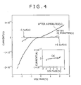
- FIG. 4 is a graph showing the current-voltage characteristic exhibited by the functional molecular element 11 based on the present embodiment of the present invention at a room temperature.
- FIG. 4 shows graph (a) obtained before the current flow, graph (b) obtained after the above-described voltage in the range of -2 V to +2 V continues to be applied for 20 minutes, and graph (c) obtained after the above-described voltage in the range of -2 V to +2 V continues to be applied for 60 minutes.
- the graphs show that the resistance of the functional molecular element 11 decreases due to the continuation of the current flow by the voltage application.
- FIG. 5 is graphs obtained by examining change in the current flowing through the functional molecular element 11 over time with variation in the applied voltage.
- the voltages given to the respective graphs are the applied voltages (V). The following tendencies can be found from FIG. 5 .
- Embodiment 2 an example of a neuron element including a functional molecular element as the above-described resistive element in an input part will be mainly described as an example relating to claims 11 to 13.
- FIG. 6 is an explanatory diagram showing the configuration of the input part and an addition part in the neuron element based on Embodiment 2 of the present invention.
- the functional molecular elements 11 equivalent to synapses are provided in an input part 10.
- the connection weight wi corresponds to the signal transmission characteristic of the synapse.
- the other electrode of the functional molecular element 11 is connected to the inverting input terminal of an OP amp (operational amplifier) 21 in the addition part 20 and is kept at the ground potential effectively.
- the current in inverse proportion to the resistance of the functional molecular element 11 is sent to the addition part 20 as a current signal equivalent to the weighed signal wixi.
- the resistance of the functional molecular element 11 decreases due to the current flowing through the functional molecular element 11 in reception of the input signal. As a result, the current flowing through the functional molecular element 11 in reception of the subsequent input signal comes to flow more easily, and thereby a learning effect is obtained. Furthermore, if reception of the input signal is absent, the resistance of the functional molecular element 11 gradually increases, so that the learning effect is obtained. Due to the accumulation and disappearance of this learning, the resistance of the functional molecular element 11 is always kept at the optimum value at the time.
- an autonomous learning function can be automatically given, and the optimum value is given as the pattern of the current flowing in the Hopfield network.
- the addition part 20 is a current-voltage conversion circuit formed of the OP amp (operational amplifier) 21.
- the output currents from the respective input circuits 11 in the input part 10 are collected into the inverting input terminal of the OP amp 21 and flow from a feedback resistor 22.
- a voltage signal corresponding to the total sum (net value) X defined by the following equation is output to an output circuit.
- X w ⁇ 1 ⁇ x ⁇ 1 + w ⁇ 2 ⁇ x ⁇ 2 + ⁇ + wnxn
- the output part is formed of an OP amp or the like and formed with e.g. a circuit that can generate a sigmoid function as the output.
- the present invention can contribute to enhancement in the performance of a neural network information processing device applied to pattern recognition by parallel distributed processing, combinatorial optimization problem and inverse matrix calculation involving many variables, associative memory, and various fields in which autonomous learning is necessary, at all of which the von Neumann computer is no good.
Landscapes
- Engineering & Computer Science (AREA)
- Physics & Mathematics (AREA)
- Theoretical Computer Science (AREA)
- Life Sciences & Earth Sciences (AREA)
- Biophysics (AREA)
- Biomedical Technology (AREA)
- Microelectronics & Electronic Packaging (AREA)
- Chemical & Material Sciences (AREA)
- Mathematical Physics (AREA)
- Health & Medical Sciences (AREA)
- Software Systems (AREA)
- General Physics & Mathematics (AREA)
- Computational Linguistics (AREA)
- Data Mining & Analysis (AREA)
- Evolutionary Computation (AREA)
- General Health & Medical Sciences (AREA)
- Molecular Biology (AREA)
- Computing Systems (AREA)
- General Engineering & Computer Science (AREA)
- Artificial Intelligence (AREA)
- Nanotechnology (AREA)
- Organic Chemistry (AREA)
- Manufacturing & Machinery (AREA)
- Crystallography & Structural Chemistry (AREA)
- Spectroscopy & Molecular Physics (AREA)
- Electromagnetism (AREA)
- Neurology (AREA)
- Electroluminescent Light Sources (AREA)
- Semiconductor Memories (AREA)
- Logic Circuits (AREA)
Applications Claiming Priority (2)
| Application Number | Priority Date | Filing Date | Title |
|---|---|---|---|
| JP2007156982A JP5104052B2 (ja) | 2007-06-14 | 2007-06-14 | 抵抗素子、ニューロン素子、及びニューラルネットワーク情報処理装置 |
| PCT/JP2008/059720 WO2008152908A1 (ja) | 2007-06-14 | 2008-05-27 | 抵抗素子、ニューロン素子、及びニューラルネットワーク情報処理装置 |
Publications (2)
| Publication Number | Publication Date |
|---|---|
| EP2157604A1 true EP2157604A1 (de) | 2010-02-24 |
| EP2157604A4 EP2157604A4 (de) | 2011-10-26 |
Family
ID=40129520
Family Applications (1)
| Application Number | Title | Priority Date | Filing Date |
|---|---|---|---|
| EP08764748A Withdrawn EP2157604A4 (de) | 2007-06-14 | 2008-05-27 | Widerstandselement, neuronenelement und vorrichtung zur verarbeitung von informationen über neuronale netzwerke |
Country Status (4)
| Country | Link |
|---|---|
| US (1) | US20100217735A1 (de) |
| EP (1) | EP2157604A4 (de) |
| JP (1) | JP5104052B2 (de) |
| WO (1) | WO2008152908A1 (de) |
Families Citing this family (6)
| Publication number | Priority date | Publication date | Assignee | Title |
|---|---|---|---|---|
| US9015093B1 (en) | 2010-10-26 | 2015-04-21 | Michael Lamport Commons | Intelligent control with hierarchical stacked neural networks |
| US8775341B1 (en) | 2010-10-26 | 2014-07-08 | Michael Lamport Commons | Intelligent control with hierarchical stacked neural networks |
| JP6708146B2 (ja) * | 2017-03-03 | 2020-06-10 | 株式会社デンソー | ニューラルネットワーク回路 |
| US11501140B2 (en) | 2018-06-19 | 2022-11-15 | International Business Machines Corporation | Runtime reconfigurable neural network processor core |
| US12141676B2 (en) * | 2019-01-14 | 2024-11-12 | Tetramem Inc. | Implementing hardware neurons using tunneling devices |
| CN115456158B (zh) * | 2022-07-26 | 2025-06-03 | 西安电子科技大学 | 基于两段式法布里珀罗激光器实现光子脉冲神经元的方法 |
Family Cites Families (14)
| Publication number | Priority date | Publication date | Assignee | Title |
|---|---|---|---|---|
| JPH03255668A (ja) * | 1989-10-23 | 1991-11-14 | Matsushita Giken Kk | 擬似神経機能回路 |
| JPH03144785A (ja) | 1989-10-31 | 1991-06-20 | Fujitsu Ltd | ニューロ素子 |
| US5223750A (en) * | 1990-06-04 | 1993-06-29 | Matsushita Research Institute Tokyo, Inc. | Artificial neural function circuit having organic thin film elements |
| JPH0512466A (ja) | 1991-07-01 | 1993-01-22 | Toshiba Corp | ニユーラルネツトワーク装置 |
| JPH0620074A (ja) * | 1992-07-02 | 1994-01-28 | Canon Inc | ニューロコンピュータ用電子素子 |
| US6128214A (en) * | 1999-03-29 | 2000-10-03 | Hewlett-Packard | Molecular wire crossbar memory |
| US6844582B2 (en) | 2002-05-10 | 2005-01-18 | Matsushita Electric Industrial Co., Ltd. | Semiconductor device and learning method thereof |
| US7408184B2 (en) * | 2002-12-25 | 2008-08-05 | Sony Corporation | Functional molecular element and functional molecular device |
| JP2004319651A (ja) * | 2003-04-14 | 2004-11-11 | Seiko Epson Corp | メモリの素子及びその製造方法 |
| JP4676704B2 (ja) * | 2004-02-10 | 2011-04-27 | ソニー株式会社 | 機能性分子素子 |
| JP4347095B2 (ja) * | 2004-03-12 | 2009-10-21 | ソニー株式会社 | 面積変調素子 |
| JP4910314B2 (ja) * | 2005-06-13 | 2012-04-04 | ソニー株式会社 | 機能性分子素子及び機能性分子装置 |
| JP4728055B2 (ja) * | 2005-06-24 | 2011-07-20 | エルピーダメモリ株式会社 | 人工神経回路 |
| JP4883796B2 (ja) * | 2007-07-23 | 2012-02-22 | キヤノン株式会社 | 電気化学測定方法 |
-
2007
- 2007-06-14 JP JP2007156982A patent/JP5104052B2/ja not_active Expired - Fee Related
-
2008
- 2008-05-27 EP EP08764748A patent/EP2157604A4/de not_active Withdrawn
- 2008-05-27 US US12/664,593 patent/US20100217735A1/en not_active Abandoned
- 2008-05-27 WO PCT/JP2008/059720 patent/WO2008152908A1/ja not_active Ceased
Also Published As
| Publication number | Publication date |
|---|---|
| JP5104052B2 (ja) | 2012-12-19 |
| WO2008152908A1 (ja) | 2008-12-18 |
| US20100217735A1 (en) | 2010-08-26 |
| JP2008311381A (ja) | 2008-12-25 |
| EP2157604A4 (de) | 2011-10-26 |
Similar Documents
| Publication | Publication Date | Title |
|---|---|---|
| Burr et al. | Neuromorphic computing using non-volatile memory | |
| EP1483737B1 (de) | Physischer neuronaler netzwerkentwurf unter verwendung von nanotechnologie | |
| Monalisha et al. | Emulation of synaptic plasticity on a cobalt-based synaptic transistor for neuromorphic computing | |
| Minnai et al. | Facile fabrication of complex networks of memristive devices | |
| EP2157604A1 (de) | Widerstandselement, neuronenelement und vorrichtung zur verarbeitung von informationen über neuronale netzwerke | |
| Hansen et al. | Unsupervised Hebbian learning experimentally realized with analogue memristive crossbar arrays | |
| Kheirabadi et al. | Neuromorphic liquids, colloids, and gels: A review | |
| Giovinazzo et al. | Analog control of retainable resistance multistates in HfO2 resistive-switching random access memories (ReRAMs) | |
| Wang et al. | Optoelectronic synapses based on hot-electron-induced chemical processes | |
| Papakonstantinopoulos et al. | Highly flexible artificial synapses from SiO2-based conductive bridge memristors and Pt nanoparticles through a crack suppression technique | |
| Sheridan et al. | Memristors and memristive devices for neuromorphic computing | |
| Chen et al. | Synaptic plasticity of a microfluidic memristor with a temporary memory function based on an ionic liquid in a capillary tube | |
| Guo et al. | A diffusive artificial synapse based on charged metal nanoparticles | |
| Beak et al. | Filamentary-based organic memristors for wearable neuromorphic computing systems | |
| Raeis-Hosseini et al. | High on/off ratio carbon quantum dot–chitosan biomemristors with coplanar nanogap electrodes | |
| Yu et al. | Gate-controlled neuromorphic functional transition in an electrochemical graphene transistor | |
| Ji et al. | High-Speed and Low-Energy Resistive Switching with Two-Dimensional Cobalt Phosphorus Trisulfide for Efficient Neuromorphic Computing | |
| JP2009157600A (ja) | ニューロン素子及びニューラルネットワーク情報処理装置 | |
| Cabaret et al. | Electro-grafted organic memristors: Properties and prospects for artificial neural networks based on STDP | |
| Wan et al. | Neuromorphic Devices for Brain-inspired Computing: Artificial Intelligence, Perception, and Robotics | |
| Bennett et al. | Supervised learning with organic memristor devices and prospects for neural crossbar arrays | |
| He et al. | Two‐Terminal Neuromorphic Memristors | |
| Bandyopadhyay et al. | Computational paradigm for nanoelectronics: self-assembled quantum dot cellular neural networks | |
| JPH03236275A (ja) | メモリ素子およびメモリ装置 | |
| Ma et al. | Optoelectronic Control of Redox Dynamics in POM Memristors for Noise‐Resilient Speech and Hardware‐Level Motion Recognition |
Legal Events
| Date | Code | Title | Description |
|---|---|---|---|
| PUAI | Public reference made under article 153(3) epc to a published international application that has entered the european phase |
Free format text: ORIGINAL CODE: 0009012 |
|
| 17P | Request for examination filed |
Effective date: 20091203 |
|
| AK | Designated contracting states |
Kind code of ref document: A1 Designated state(s): AT BE BG CH CY CZ DE DK EE ES FI FR GB GR HR HU IE IS IT LI LT LU LV MC MT NL NO PL PT RO SE SI SK TR |
|
| AX | Request for extension of the european patent |
Extension state: AL BA MK RS |
|
| DAX | Request for extension of the european patent (deleted) | ||
| A4 | Supplementary search report drawn up and despatched |
Effective date: 20110927 |
|
| RIC1 | Information provided on ipc code assigned before grant |
Ipc: H01L 51/00 20060101ALN20110921BHEP Ipc: G06N 3/00 20060101ALI20110921BHEP Ipc: G06N 3/063 20060101AFI20110921BHEP |
|
| 17Q | First examination report despatched |
Effective date: 20120511 |
|
| GRAP | Despatch of communication of intention to grant a patent |
Free format text: ORIGINAL CODE: EPIDOSNIGR1 |
|
| RIC1 | Information provided on ipc code assigned before grant |
Ipc: H01L 51/00 20060101ALN20130312BHEP Ipc: G06N 3/063 20060101AFI20130312BHEP Ipc: G06N 3/00 20060101ALI20130312BHEP |
|
| INTG | Intention to grant announced |
Effective date: 20130410 |
|
| STAA | Information on the status of an ep patent application or granted ep patent |
Free format text: STATUS: THE APPLICATION IS DEEMED TO BE WITHDRAWN |
|
| 18D | Application deemed to be withdrawn |
Effective date: 20130821 |