EP2148341A1 - Electrode foil, process for producing the electrode foil, and electrolytic capacitor - Google Patents
Electrode foil, process for producing the electrode foil, and electrolytic capacitor Download PDFInfo
- Publication number
- EP2148341A1 EP2148341A1 EP08751579A EP08751579A EP2148341A1 EP 2148341 A1 EP2148341 A1 EP 2148341A1 EP 08751579 A EP08751579 A EP 08751579A EP 08751579 A EP08751579 A EP 08751579A EP 2148341 A1 EP2148341 A1 EP 2148341A1
- Authority
- EP
- European Patent Office
- Prior art keywords
- foil
- aluminum
- particles
- film
- electrolytic capacitor
- Prior art date
- Legal status (The legal status is an assumption and is not a legal conclusion. Google has not performed a legal analysis and makes no representation as to the accuracy of the status listed.)
- Withdrawn
Links
Images








Classifications
-
- H—ELECTRICITY
- H01—ELECTRIC ELEMENTS
- H01G—CAPACITORS; CAPACITORS, RECTIFIERS, DETECTORS, SWITCHING DEVICES, LIGHT-SENSITIVE OR TEMPERATURE-SENSITIVE DEVICES OF THE ELECTROLYTIC TYPE
- H01G9/00—Electrolytic capacitors, rectifiers, detectors, switching devices, light-sensitive or temperature-sensitive devices; Processes of their manufacture
- H01G9/004—Details
- H01G9/04—Electrodes or formation of dielectric layers thereon
- H01G9/042—Electrodes or formation of dielectric layers thereon characterised by the material
- H01G9/045—Electrodes or formation of dielectric layers thereon characterised by the material based on aluminium
-
- H—ELECTRICITY
- H01—ELECTRIC ELEMENTS
- H01G—CAPACITORS; CAPACITORS, RECTIFIERS, DETECTORS, SWITCHING DEVICES, LIGHT-SENSITIVE OR TEMPERATURE-SENSITIVE DEVICES OF THE ELECTROLYTIC TYPE
- H01G11/00—Hybrid capacitors, i.e. capacitors having different positive and negative electrodes; Electric double-layer [EDL] capacitors; Processes for the manufacture thereof or of parts thereof
- H01G11/22—Electrodes
- H01G11/30—Electrodes characterised by their material
- H01G11/48—Conductive polymers
-
- H—ELECTRICITY
- H01—ELECTRIC ELEMENTS
- H01G—CAPACITORS; CAPACITORS, RECTIFIERS, DETECTORS, SWITCHING DEVICES, LIGHT-SENSITIVE OR TEMPERATURE-SENSITIVE DEVICES OF THE ELECTROLYTIC TYPE
- H01G9/00—Electrolytic capacitors, rectifiers, detectors, switching devices, light-sensitive or temperature-sensitive devices; Processes of their manufacture
- H01G9/004—Details
- H01G9/02—Diaphragms; Separators
-
- H—ELECTRICITY
- H01—ELECTRIC ELEMENTS
- H01G—CAPACITORS; CAPACITORS, RECTIFIERS, DETECTORS, SWITCHING DEVICES, LIGHT-SENSITIVE OR TEMPERATURE-SENSITIVE DEVICES OF THE ELECTROLYTIC TYPE
- H01G9/00—Electrolytic capacitors, rectifiers, detectors, switching devices, light-sensitive or temperature-sensitive devices; Processes of their manufacture
- H01G9/004—Details
- H01G9/022—Electrolytes; Absorbents
- H01G9/025—Solid electrolytes
- H01G9/028—Organic semiconducting electrolytes, e.g. TCNQ
-
- H—ELECTRICITY
- H01—ELECTRIC ELEMENTS
- H01G—CAPACITORS; CAPACITORS, RECTIFIERS, DETECTORS, SWITCHING DEVICES, LIGHT-SENSITIVE OR TEMPERATURE-SENSITIVE DEVICES OF THE ELECTROLYTIC TYPE
- H01G9/00—Electrolytic capacitors, rectifiers, detectors, switching devices, light-sensitive or temperature-sensitive devices; Processes of their manufacture
- H01G9/004—Details
- H01G9/04—Electrodes or formation of dielectric layers thereon
- H01G9/048—Electrodes or formation of dielectric layers thereon characterised by their structure
- H01G9/055—Etched foil electrodes
-
- H—ELECTRICITY
- H01—ELECTRIC ELEMENTS
- H01G—CAPACITORS; CAPACITORS, RECTIFIERS, DETECTORS, SWITCHING DEVICES, LIGHT-SENSITIVE OR TEMPERATURE-SENSITIVE DEVICES OF THE ELECTROLYTIC TYPE
- H01G9/00—Electrolytic capacitors, rectifiers, detectors, switching devices, light-sensitive or temperature-sensitive devices; Processes of their manufacture
- H01G9/15—Solid electrolytic capacitors
- H01G9/151—Solid electrolytic capacitors with wound foil electrodes
-
- Y—GENERAL TAGGING OF NEW TECHNOLOGICAL DEVELOPMENTS; GENERAL TAGGING OF CROSS-SECTIONAL TECHNOLOGIES SPANNING OVER SEVERAL SECTIONS OF THE IPC; TECHNICAL SUBJECTS COVERED BY FORMER USPC CROSS-REFERENCE ART COLLECTIONS [XRACs] AND DIGESTS
- Y02—TECHNOLOGIES OR APPLICATIONS FOR MITIGATION OR ADAPTATION AGAINST CLIMATE CHANGE
- Y02E—REDUCTION OF GREENHOUSE GAS [GHG] EMISSIONS, RELATED TO ENERGY GENERATION, TRANSMISSION OR DISTRIBUTION
- Y02E60/00—Enabling technologies; Technologies with a potential or indirect contribution to GHG emissions mitigation
- Y02E60/13—Energy storage using capacitors
-
- Y—GENERAL TAGGING OF NEW TECHNOLOGICAL DEVELOPMENTS; GENERAL TAGGING OF CROSS-SECTIONAL TECHNOLOGIES SPANNING OVER SEVERAL SECTIONS OF THE IPC; TECHNICAL SUBJECTS COVERED BY FORMER USPC CROSS-REFERENCE ART COLLECTIONS [XRACs] AND DIGESTS
- Y10—TECHNICAL SUBJECTS COVERED BY FORMER USPC
- Y10T—TECHNICAL SUBJECTS COVERED BY FORMER US CLASSIFICATION
- Y10T428/00—Stock material or miscellaneous articles
- Y10T428/12—All metal or with adjacent metals
- Y10T428/12014—All metal or with adjacent metals having metal particles
- Y10T428/12028—Composite; i.e., plural, adjacent, spatially distinct metal components [e.g., layers, etc.]
- Y10T428/12049—Nonmetal component
-
- Y—GENERAL TAGGING OF NEW TECHNOLOGICAL DEVELOPMENTS; GENERAL TAGGING OF CROSS-SECTIONAL TECHNOLOGIES SPANNING OVER SEVERAL SECTIONS OF THE IPC; TECHNICAL SUBJECTS COVERED BY FORMER USPC CROSS-REFERENCE ART COLLECTIONS [XRACs] AND DIGESTS
- Y10—TECHNICAL SUBJECTS COVERED BY FORMER USPC
- Y10T—TECHNICAL SUBJECTS COVERED BY FORMER US CLASSIFICATION
- Y10T428/00—Stock material or miscellaneous articles
- Y10T428/12—All metal or with adjacent metals
- Y10T428/12014—All metal or with adjacent metals having metal particles
- Y10T428/12028—Composite; i.e., plural, adjacent, spatially distinct metal components [e.g., layers, etc.]
- Y10T428/12063—Nonparticulate metal component
- Y10T428/12139—Nonmetal particles in particulate component
Definitions
- the present invention relates to an electrode foil suitable as the anode foil in an electrolytic capacitor, a method of manufacturing such an electrode foil, and an electrolytic capacitor.
- Aluminum electrode foils for electrolytic capacitors are generally produced using as the starting material at least 98% high-purity aluminum that has been rendered into the form of a foil by rolling. Innumerable pits are formed on the surface of the aluminum foil using a known direct-current electrolytic etching process, an alternating-current electrolytic etching process, or both in alternation, within an acid or alkali solution that dissolves aluminum, thereby enlarging the actual surface area and increasing the electrostatic capacitance.
- electrolytic capacitors are composed of an extremely thin oxide film layer, the electrostatic capacitance per unit surface area of the electrode is high, enabling electrolytic capacitors which are small yet of large capacitance to be obtained.
- electrolytic capacitors of even smaller size and higher capacitance.
- the entire aluminum foil becomes filled with etching pits, which makes the electrode foil fragile and lowers the electrode foil strength.
- one method for achieving a large electrode foil surface area while maintaining the foil strength is to etch an aluminum foil of substantial thickness and thereby increase the capacitance per unit surface area.
- the capacitance per unit surface area is large, but when such an electrode foil is used to construct a common coiled electrolytic capacitor, the large thickness of the electrode foil places limits on the length of electrode foil that may be used, resulting in the formation of a capacitor element which will not fit within the case.
- the number of stacked layers may be increased or thick electrode foils may be used, resulting in an increase in the height of the capacitor.
- Patent Document 1 In addition to the general prior art mentioned above, in the case of coiled electrolytic capacitors, as described in Patent Document 1, a method is known which, based on the fact that the capacitance is computed as the composite capacitance, increases the capacitance by forming a vapor-deposited film of metal nitride on a substrate surface. Also, Patent Document 2 discloses a method for achieving an increased capacitance by using foil which has been brought into physical contact with carbon as the cathode to cancel the cathode-side capacitance so that only the anode-side capacitance is reflected in the composite capacitance.
- Electrolytic capacitors are electronic components which are widely used in electronic devices, and generally have the following type of construction.
- valve action The action of having resistance to a voltage applied in one direction but losing such resistance when a voltage is applied in the opposite direction is called a "valve action.”
- An electrolytic capacitor uses a valve metal (e.g., aluminum) having such a valve action as the anode.
- a valve metal e.g., aluminum
- an insulating oxide film is formed on the anode surface.
- This oxide film acts as a dielectric layer; an electrolyte such as an electrolytic solution or an electrically conductive polymer, or a solid electrolyte, is in contact with the oxide film substantially as a cathode.
- an electrolyte such as an electrolytic solution or an electrically conductive polymer, or a solid electrolyte
- the electrolyte In a coiled capacitor, the electrolyte is held by electrolytic paper (separator) or the like. In a flat-plate capacitor, a carbon paste and metal particles with a resin material are formed on the electrolyte in this order, resulting in a cathode layer.
- the cathode-side electrode is led out from a cathode made of a metal such as aluminum.
- the anode-side electrode and the cathode-side electrode are generally made of foils that have been cut into strips.
- the capacitor element is formed by winding the foils together with a separator.
- the capacitor element is formed by arranging as an anode-side electrode, a cathode layer, and a cathode-side electrode or the like, all of which are of square shape. Stacking together a plurality of such capacitor elements results in a multilayer capacitor.
- the cathode layer is connected to a lead-out electrode which is composed primarily of a metal and electrically connects the cathode layer to the exterior, and is thereby led out to the exterior from any of various types of housings which encase the capacitor element.
- the electrolytic capacitor is characterized by a high electrostatic capacitance per unit surface area of the electrode, enabling a small capacitor of large capacitance to be obtained.
- the miniaturization of electronic devices smaller sizes and larger capacitances are being demanded even of electrolytic capacitors.
- the entire aluminum foil becomes filled with etching pits, which makes the electrode foil fragile and lowers the electrode foil strength.
- one method for achieving a large electrode foil surface area while maintaining the foil strength is to etch an aluminum foil of substantial thickness and thereby increase the capacitance per unit surface area.
- the capacitance per unit surface area is large, but when such an electrode foil is used to construct common coiled electrolytic capacitors, the large thickness of the electrode foil places limits on the length of electrode foil that may be used, resulting in the formation of a capacitor element which will not fit within the case.
- the number of stacked layers may be increased or thick electrode foils may be used, resulting in an increase in the height of the capacitor.
- Patent Document 1 Japanese Laid-open Patent Publication No. 02-117123
- Patent Document 2 Japanese Patent No. 3,875,705
- a second object of the invention is to provide an anodic electrode foil structure which dramatically increases the anode foil surface area that relates to the capacitance of a capacitor while retaining a thickness, strength and voltage resistance comparable to the prior art, and to provide a large-capacitance electrolytic capacitor which uses the same.
- the electrode foil according to the present invention is characterized by having a structure in which metal particles and ceramic particles, which primarily include at least one of valve metal particles having a dielectric constant and ceramic particles, are deposited on a surface of a metal foil.
- the electrode foil is characterized in that the deposit of the metal particles and/or ceramic particles is formed by using aerosol deposition.
- the method of manufacturing an electrode foil according to the present invention is characterized by placing an aluminum foil in a film-forming chamber of an aerosol chamber, aerosolizing aluminum powder, and spraying the aerosolized aluminum powder onto the aluminum foil placed in the film-forming chamber so as to deposit aluminum particles on the aluminum foil.
- the surface of aluminum foil or on the surface of etched foil obtained by electrolytically etching the surface of aluminum foil by in this way uniformly diffusing an ultrafine powder having a dielectric constant in a high-velocity gas and spraying the gas onto a surface of metal foil or etched foil serving as the target so as to form a formed film of ultrafine powder, then individually etching the particles of the fine powder, compared with conventional etched foil composed of aluminum alone, the surface area of aluminum may be increased in foil of the same thickness.
- a first aspect of the invention provides an electrolytic capacitor having an anode foil composed of a metal with a valve action, a cathode layer, and an electrolyte layer interposed between the anode foil and the cathode layer, the capacitor being characterized in that the anode foil has on a surface thereof a dielectric oxide film layer formed by using an aerosol deposition method to deposit particles having a dielectric constant.
- the anode foil is a flat rolled aluminum foil or an aluminum foil having a rough, etched surface, and the particles having a dielectric constant in the layer deposited on the anode foil are valve metal particles composed primarily of valve metal.
- the particles having a dielectric constant in the layer deposited on the anode foil further contain ceramic particles composed primarily of a ceramic.
- the electrolytic capacitors may have a layer formed by depositing valve metal particles having a high dielectric constant on the anode foil by an aerosol deposition process, anode foil having a larger surface area per unit surface area of the anode foil than etched anode foils used in conventional electrolytic capacitors may be obtained.
- an electrolytic capacitor in which such an anode foil is used as an anodic electrode has a high electrolytic capacitance compared with prior-art electrolytic capacitors, enabling a small, high-capacitance electrolytic capacitor to be obtained.
- anode foil By additionally etching the above layer of valve metal particles deposited by an aerosol deposition process and the above anode foil, it is possible to increase the surface area of the deposited layer and the anode foil, enabling the capacitance of the electrolytic capacitor to be made even higher.
- the anode foil may also be subjected to etching treatment prior to the particle deposition step by aerosol deposition as described above.
- the treated electrode foil By subjecting the treated electrode foil to conversion treatment at a suitable applied voltage, it is possible to ensure voltage resistance. Moreover, compared with conventional etched and conversion-treated foil, there is also the advantage that the thickness of the deposited layer of valve metal particles may be adjusted by adjusting the blowing velocity and blowing time in the aerosol deposition process, making it possible to adjust the capacitance.
- anode foil fabricated by such a manufacturing process as the anode foil in coiled electrolytic capacitors, single-layer capacitors and multilayer capacitors, it is possible to achieve a larger capacitance in these capacitors.
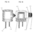
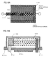
- FIG. 1 is a schematic view illustrating the structure of a coiled electrolytic capacitor serving as an embodiment in which an electrode foil according to the invention is employed as an anode foil.
- FIG. 1A illustrates the outside appearance of the capacitor
- FIG. 1B illustrates a perspective view to the interior with the housing (metal case) 10 removed.
- An anodic electrode lead 12 and a cathodic electrode lead 13 are fixed to a sealant (insulating resin) 11.
- a wound capacitor element 20 is fixed to the sealant (insulating resin) 11 within the housing (metal case) 10, and the anodic electrode lead 12 and the cathodic electrode lead 13 are electrically connected to, respectively, an anode foil 21 (which is an electrode foil according to the invention) and a cathode foil 22.
- the anode foil 21 and the cathode foil 22 are cylindrically coiled with electrolytic paper 23 as a separator therebetween, and the final ends of the foils are fixed with tape 24 to maintain the coiled state.
- Electrolytic capacitors which use the electrode foil of the invention achieve a higher capacitance than electrolytic capacitors of prior-art construction which use an etched electrode foil obtained by electrolytically etching the aluminum foil intended for use as the anode foil.
- the electrode foil according to the invention is characterized by having a structure obtained by uniformly dispersing in a high-velocity gas an ultrafine powder of metal having a particle size in a range of from 100 nm to 100 ⁇ m, an ultrafine powder including the above ultrafine powder of metal and/or an oxide, a nitride or a carbide having a high dielectric constant of 10 or more, or an ultrafine powder of valve metal that has been oxidized at the surface and has a particle size of 500 nm or less, and spraying the resulting gas onto the surface of the etched electrode foil serving as the target, so as to form a foremed film of the ultrafine powder on the surface of a prior-art metal foil or an etched metal foil obtained by etching a prior-art metal foil.
- valve metal particles include at least one from among valve metal aluminum and compounds thereof, titanium and compounds thereof, tantalum and compounds thereof, and niobium and compounds thereof.
- electrode foil in which the surface area of aluminum has been increased may be obtained in electrode foil of the same thickness.
- a formed film of ultrafine powder that has been formed on the surface of the etched electrode foil may be electrolytically etched.
- electrode foil in which the surface area of aluminum has been increased may be obtained in electrode foil of the same thickness.
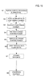
- FIG. 2 is a flow chart illustrating the sequence of steps in a method of manufacturing an electrode foil in a first embodiment according to the invention. Illustrations of the states corresponding to the treatment steps are illustrated on the left side of the flow chart.
- Aluminum foil 21 (purity, 99%) having a thickness of 40 ⁇ m was prepared by rolling (Step S1: State I).
- FIG. 3 is a schematic diagram of an exemplary aerosol deposition chamber configuration.
- a film-forming chamber 303 has a stage 304 which is movable in the X and Y directions in the interior thereof.
- the rolled aluminum foil 21 prepared in Step S1 is affixed to the stage 304 (Step S2).
- the interior of the film-forming chamber 303 was evacuated using a vacuum pump 306, thereby lowering the pressure beforehand to 10 Pa or below (Step S3).
- a starting powder 300 composed primarily of a powder of aluminum, which is a valve metal, having an average particle size of 8 ⁇ m was placed in an aerosol generator 301A, ultrasound was applied to the entire aerosol generator 301A by an oscillator 301B, and degassing in vacuum was carried out for 30 minutes while heating at about 150°C, thereby effecting pretreatment in which moisture that had formed on the powder surface is removed (Step S4).
- High-purity helium gas (gas pressure, 2 kg/cm 2 ; gas flow rate, 10 L/min) 302 was introduced into the aerosol generator 301A, and the pretreated starting powder 300 was aerosolized (Step S5).
- this aerosol was passed through a pipe and delivered to the film-forming chamber 303 by a nozzle 305.
- the nozzle 305 used was one having a helical groove formed on the inside. Spraying was carried out for 3 minutes from a nozzle 305 having a helical groove on the inside toward the aluminum foil substrate 21 (Step S6). The pressure within the chamber at this time was fixed at 500 Pa.
- the aluminum film 201A which was formed of fine particles of aluminum on the top surface of the aluminum foil substrate 21 by aerosol deposition in this way, had a thickness of 20 ⁇ m (State II: aerosol deposition with fine aluminum particles).
- Step S7 annealing the deposited aluminum metal particle in an inert gas at 300°C, which is a temperature at or below the melting point of aluminum + 100°C, thereby carrying out sintering pretreatment in which the deposited aluminum metal particles are densified.
- This foil was electrolytically treated for 8 minutes in an aqueous solution of hydrochloric acid, nitric acid and AlCl 3 at a current density of 0.2 A/m 2 (50 Hz), thereby carrying out roughening treatment (etching) (Step S7).
- This etching treatment resulted in the formation of a microcavity layer 201B (State III).
- Step S8 conversion treatment was carried out in an aqueous solution of ammonium borate/ammonium adipate.
- Such treatment enlarges the surface area by forming a microcavity layer 201B, in addition the surface 201C of the microcavity layer 201B is oxidized by the conversion treatment in Step S8, resulting in the formation of a dielectric oxide film layer 200 having a large dielectric constant on the surface of the aluminum foil substrate 21 (State IV).
- a structure, where metal particles are stacked with gaps which are smaller than the metal particles, is formed on the surface of the metal foil, making it possible to achieve a structure in which an oxide film is formed on the surface of the metal particles.
- the leak current of the dielectric oxide film layer 200 which was formed by the treatment process in FIG. 2 , was measured after an applied voltage had reached to predetermined voltage of 20 V and 30 minutes had passed thereafter. In addition, the tensile strength of the film was measured.
- the tensile strength was measured by cutting out test pieces having a width of 1 cm and a length of 5 cm, and subjecting the test pieces to strain on a tensile testing machine at a test rate of 10 mm/min. If the strength at break was 1.5 kg/cm (not normalized by thickness; this value is specified based on the two-dimensional shape of the test piece) or more, the piece was rated as acceptable.
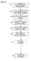
- FIG. 4 is a flow chart illustrating the sequence of steps in a method of manufacturing an electrode foil in a second embodiment according to the invention.
- a first embodiment according to the flow chart in FIG. 2 above an example was described in which 99% aluminum foil substrate 21 having a thickness of 40 ⁇ m obtained by rolling was used as the electrode foil.
- an etched aluminum foil with a rough surface (etched surface) 201 subjected beforehand to etching treatment as illustrated in FIG. 5A which has also been used in the prior art, was used.
- the roughened aluminum foil was subjected to the treatments in Steps S2 to S8 in the same way as the treatment sequence in FIG. 2 explained earlier for the first embodiment.
- the etching treatment in Step S7 of FIG. 2 was omitted.
- FIG. 5B schematically illustrates the cross-section of a layer 202 obtained as described above using aerosol deposition to deposit fine particles of aluminum on a rough surface 201 that was subjected to etching treatment beforehand.
- the leakage current 30 minutes after reaching a predetermined voltage of 20 V was measured.
- the tensile strength was measured by cutting out test pieces having a width of 1 cm and a length of 5 cm, and subjecting them to strain on a tensile testing machine at a test rate of 10 mm/min. If the strength at break was 1.5 kg/cm (not normalized by thickness; this value is specified based on the two-dimensional shape of the test piece) or more, the piece was rated as acceptable. In addition, the tensile strength of the film foil was measured.
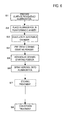
- FIG. 6 is a flow chart illustrating the sequence of steps in a method of manufacturing an electrode foil in a third embodiment according to the invention.
- 99% aluminum foil having a thickness of 40 ⁇ m obtained by rolling was annealed at 300°C in an inert gas, thereby carrying out pretreatment.
- This foil was electrolytically treated for 8 minutes at a current density of 0.2 A/m 2 (50 Hz) in an aqueous solution of hydrochloric acid, nitric acid and AlCl 3 , thereby carrying out surface roughening treatment.
- an etched aluminum foil 21 having the rough surface (etched surface) 201 in FIG. 5A was obtained (Step S1).
- the etched aluminum foil 21 (see FIG. 5A ) was subjected as described below to surface treatment in the aerosol deposition chamber illustrated in FIG. 2 in accordance with the flow in FIG. 6 .
- the rolled aluminum foil 21 prepared in Step S1 was affixed to a stage 304 which is movable in the X and Y directions within the film-forming chamber 303 (Step S2).
- the interior of the film-forming chamber 303 was evacuated using a vacuum pump 306, thereby lowering the pressure beforehand to 10 Pa or below (Step S3).
- ultrafine ceramic particles of barium titanate having an average particle size of 100 nm were placed in an aerosol generator 301A as the starting powder 300, ultrasound was applied to the entire aerosol generator 301A by an oscillator 301B, and degassing in vacuum was carried out for 30 minutes while heating at about 150°C, thereby effecting pretreatment in which moisture that had formed on the powder surface is removed (Step S4).
- High-purity helium gas (gas pressure, 2 kg/cm 2 ; gas flow rate, 10 L/min) 302 was introduced into the aerosol generator 301A, and the pretreated starting powder 300 was aerosolized (Step S5).
- this aerosol was passed through a pipe and delivered to the film-forming chamber 303 by a nozzle 305.
- the nozzle 305 used was one having a helical groove formed on the inside. Spraying was carried out for 3 minutes from a nozzle 305 having a helical groove on the inside toward the aluminum foil substrate 21 (Step S6). The pressure within the chamber at this time was fixed at 500 Pa.
- the ceramic (barium titanate) film which was formed of fine particles on the top surface of the aluminum foil substrate 21 by aerosol deposition in this way, had a thickness of 2 ⁇ m.
- Step S8 conversion treatment was carried out in an aqueous solution of ammonium adipate.
- the dielectric oxide film layer 200 formed by the above treatment steps illustrated in FIG. 6 was then subjected to leakage current measurement 30 minutes after reaching a predetermined voltage of 20 V. The tensile strength of the film was also measured.
- Tensile strength measurement was performed by cutting out test pieces having a width of 1 cm and a length of 5 cm, and subjecting them to strain on a tensile testing machine at a test rate of 10 mm/min. If the strength at break was 1.5 kg/cm (not normalized by thickness; this value is specified based on the two-dimensional shape of the test piece) or more, the piece was rated as acceptable.
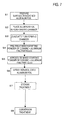
- FIG. 7 is a flow chart illustrating the sequence of steps in a method of manufacturing an electrode foil in a fourth embodiment according to the invention.
- 99% aluminum foil having a thickness of 40 ⁇ m obtained by rolling was annealed at 300°C in an inert gas, thereby carrying out pretreatment was carried out.
- This foil was electrolytically treated for 8 minutes at a current density of 0.2 A/m 2 (50 Hz) in an aqueous solution of hydrochloric acid, nitric acid and AlCl 3 , thereby carrying out surface roughening treatment.
- an aluminum foil 21 having the etched surface 201 in FIG. 5A was obtained (Step S1).
- the etched aluminum foil 21 (see FIG. 5A ) was subjected as described below to surface treatment in the aerosol deposition chamber illustrated in FIG. 2 in accordance with the flow chart in FIG. 7 .
- the rolled aluminum foil 21 prepared in Step S1 was affixed to a stage 304 which is movable in the X and Y directions within the film-forming chamber 303 (Step S2).
- the interior of the film-forming chamber 303 was evacuated using a vacuum pump 306, thereby lowering the pressure beforehand to 10 Pa or below (Step S3).
- Step S4 a mixture of ultrafine ceramic particles of barium titanate having an average particle size of 100 nm and ultrafine aluminum powder having an average particle size of 8 ⁇ m was placed in an aerosol generator 301A as the starting powder 300, ultrasound was applied to the entire aerosol generator 301A by an oscillator 301B, and degassing in vacuum was carried out for 30 minutes while heating at about 150°C, thereby effecting pretreatment in which moisture that had formed on the powder surface is removed (Step S4).
- High-purity helium gas (gas pressure, 2 kg/cm 2 ; gas flow rate, 10 L/min) 302 was introduced into the aerosol generator 301A, and the pretreated starting powder 300 was aerosolized (Step S5).
- this aerosol was passed through a pipe and delivered to the film-forming chamber 303 by a nozzle 305.
- the nozzle 305 used was one having a helical groove formed on the inside. Spraying was carried out for 3 minutes from a nozzle 305 having a helical groove on the inside toward the aluminum foil substrate 21 (Step S6). The pressure within the chamber at this time was fixed at 500 Pa.
- the ceramic (barium titanate) - aluminum film 200 which was formed of fine particles of ceramic 202a and fine particles of aluminum 202b on the top surface of the aluminum foil substrate 21 by aerosol deposition as illustrated in FIG. 8 , had a thickness of 20 ⁇ m.
- Step S8 conversion treatment was carried out in an aqueous solution of ammonium adipate.
- the dielectric oxide film layer 200 formed by the above treatment steps illustrated in FIG. 7 was then subjected to leakage current measurement 30 minutes after reaching a predetermined voltage of 20 V. The tensile strength of the film was also measured.
- the tensile strength was measured by cutting out test pieces having a width of 1 cm and a length of 5 cm, and subjecting them to strain on a tensile testing machine at a test rate of 10 mm/min. If the strength at break was 1.5 kg/cm (not normalized by thickness; this value is specified based on the two-dimensional shape of the test piece) or more, the piece was rated as acceptable.
- a comparative example for comparison with the above first to fourth embodiments was carried out as follows.
- Aluminum foil (99%) having a thickness of 40 ⁇ m obtained by rolling was annealed at 300°C in an inert gas, thereby carrying out pretreatment.
- This foil was electrolytically treated for 8 minutes at a current density of 0.2 A/m 2 (50 Hz) in an aqueous solution of hydrochloric acid, nitric acid and AlCl 3 , thereby carrying out surface roughening treatment.
- conversion treatment in an aqueous solution of ammonium adipate was carried out.
- the leakage current 30 minutes after reaching a predetermined voltage of 20 V was measured.
- the tensile strength of the film was measured.
- Tensile strength measurement was performed by cutting out test pieces having a width of 1 cm and a length of 5 cm, and subjecting them to strain on a tensile testing machine at a test rate of 10 mm/min. If the strength at break was 1.5 kg/cm (not normalized by thickness; this value is specified based on the two-dimensional shape of the test piece) or more, the piece was rated as acceptable. In addition, the tensile strength of the film was measured.
- Table 1 below is a table comparing the above first to fourth embodiments and the comparative example.
- the tensile strength of the foils in the first to fourth embodiments are higher than in the comparative example.
- the electrostatic capacitance per unit surface area in the second to fourth embodiments was from 150 to 180 ⁇ F, which was about four times the value of 40 ⁇ F in the comparative example.
- This invention thus makes it possible to provide electrolytic capacitors having an electrostatic capacitance about four times that of prior-art electrolytic capacitors.
- valve metal particles that are deposited may be adjusted after taking into consideration the relationship between the voltage resistance and capacitance of the films obtained by the aerosol deposition process.
- a single kind of valve metal may be deposited alone.
- the electrostatic capacitance per unit surface area was obtained by measuring the electrostatic capacitance in an aqueous solution of ammonium adipate.
- FIG. 9 is a schematic view illustrating the structure of a coiled electrolytic capacitor serving as an embodiment in which the invention is employed.
- FIG. 9A illustrates the outside appearance of the capacitor
- FIG. 9B illustrates a perspective view to the interior with the housing (metal case) 510 removed.
- An anodic electrode lead 512 and a cathodic electrode lead 513 are fixed to a sealant (insulating resin) 511.
- a wound capacitor element 520 is fixed to the sealant (insulating resin) 511 within the housing (metal case) 510, and the anodic electrode lead 512 and the cathodic electrode lead 513 are electrically connected to, respectively, an anode foil 521 and a cathode foil 522.
- the anode foil 521 and the cathode foil 522 are cylindrically wound with electrolytic paper 523 as a separator therebetween, and the final ends of the foils are fixed with tape 524 to maintain the coiled state.
- the electrolytic capacitor of the invention achieves a higher capacitance than electrolytic capacitors of prior-art constructions which use an etched electrode foil obtained by electrolytically etching the aluminum foil intended for use as the anode foil.
- the inventive electrolytic capacitor is characterized by uniformly dispersing in a high-velocity gas an ultrafine powder of metal, or an ultrafine powder of metal in combination with an ultrafine powder having a high dielectric constant or an ultrafine powder of valve metal that has been oxidized at the surface, and spraying the resulting gas onto the surface of the etched electrode foil serving as the target so as to form a formed film of ultrafine powder.
- electrode foil in which the surface area of aluminum has been increased may be obtained in electrode foil of the same thickness.
- a formed film of ultrafine powder that has been additionally formed on the surface of the etched electrode foil may be electrolytically etched.
- electrode foil in which the surface area of aluminum has been further enlarged may be employed in electrode foil of the same thickness.
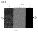
- FIG. 10 is a schematic view illustrating the cross-sectional structure of the coiled capacitor element 520 in FIG. 9 .
- the anode foil 521 and the cathode foil 522 are placed one over the another with an electrolytic paper 530 impregnated with electrolyte 531 as the separator interposed therebetween.
- the cathode foil 522 may be constructed so as to include at least one from among electrolytic paper, carbon, metal foil, metal particles and electrically conductive resin.
- an electrolytic solution obtained by dissolving an organic acid salt or an inorganic acid salt in a protic solution may be used as the electrolyte 531.
- a solid electrolytic capacitor may be obtained by using, as specific examples of the electrolyte 531, at least one solid electrolyte from among polythiophene-type, polypyrrole-type and polyaniline-type conductive polymers, and TCNQ complex salts.
- the electrolytic capacitor according to the invention has the characteristic in particular that a dielectric oxide film layer 700 is formed on the surface of the anode foil 521.
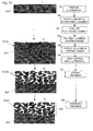
- FIG. 11 is a diagram illustrating the sequence of steps in a forming method of a fifth embodiment of a dielectric oxide film layer 700 on the surface of an anode foil 521. Figures depicting the states corresponding to the treatment steps are illustrated on the left side of the flow chart.
- Aluminum foil 521 (purity, 99%) having a thickness of 40 ⁇ m was prepared by rolling (Step S1: State I).
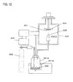
- FIG. 12 is a schematic diagram of an exemplary aerosol deposition chamber configuration.
- a film-forming chamber 303 has a stage 304 which is movable in the X and Y directions in the interior thereof.
- the rolled aluminum foil 521 prepared in Step S1 is affixed to the stage 304 (Step S2).
- the interior of the film-forming chamber 303 was evacuated using a vacuum pump 306, thereby lowering the pressure beforehand to 10 Pa or below (Step S3).
- a starting powder 300 composed primarily of a powder of aluminum, which is valve metal, having an average particle size of 8 ⁇ m was placed in an aerosol generator 301A, ultrasound was applied to the entire aerosol generator 301A by an oscillator 301B, and degassing in vacuum was carried out for 30 minutes while heating at about 150°C, thereby effecting pretreatment in which moisture that had formed on the powder surface is removed (Step S4).
- High-purity helium gas (gas pressure, 2 kg/cm 2 ; gas flow rate, 10 L/min) 302 was introduced into the aerosol generator 301A, and the pretreated starting powder 300 was aerosolized (Step S5).
- this aerosol was passed through a pipe and delivered to the film-forming chamber 303 by a nozzle 305.
- the nozzle 305 used was one having a helical groove formed on the inside. Spraying was carried out for 3 minutes from a nozzle 305 having a helical groove on the inside toward the aluminum foil substrate 521 (Step S6). The pressure within the chamber at this time was fixed at 500 Pa.
- the aluminum film 701A which was formed of fine particles of aluminum on the top surface of the aluminum foil substrate 521 by aerosol deposition in this way, had a thickness of 20 ⁇ m (State II: aerosol deposition with fine aluminum particles).
- Step S7 annealing the deposited aluminum metal particles in an inert gas at 300°C, which is a temperature at or below the melting point of aluminum + 100°C, thereby carrying out sintering pretreatment in which the deposited aluminum metal particles are densified.
- This foil was electrolytically treated for 8 minutes in an aqueous solution of hydrochloric acid, nitric acid and AlCl 3 at a current density of 0.2 A/m 2 (50 Hz), thereby carrying out roughening treatment (etching) (Step S7).
- This etching treatment resulted in the formation of a microcavity layer 701B (State III).
- Step S8 conversion treatment was carried out in an aqueous solution of ammonium borate/ammonium adipate.
- Such treatment enlarges the surface area by forming a microcavity layer 701B, in addition to which the surface 701C of the microcavity layer 701B is oxidized by conversion treatment in Step S8, resulting in the formation of a dielectric oxide film layer 700 having a large dielectric constant on the surface of the aluminum foil substrate 521 (State IV).
- an example was described in which 99% aluminum foil substrate having a thickness of 40 ⁇ m obtained by rolling was used as the anode foil 521.
- an etched aluminum foil with a rough surface (etched surface) 701 subjected beforehand to etching treatment as illustrated in FIG. 13A which has also been used in the prior art, may be used.
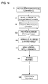
- FIG. 14 is a flow chart illustrating the sequence of steps in a method of manufacturing an electrode foil in a sixth embodiment according to the invention.
- the roughened aluminum foil was subjected to the treatments in Steps S2 to S8 in the same way as the treatment sequence in FIG. 10 explained earlier for the fifth embodiment.
- the etching treatment in Step S7 of FIG. 10 was omitted.
- FIG. 13B schematically illustrates the cross-section of a layer 702 obtained as described above using aerosol deposition to deposit fine particles of aluminum on the rough surface 701 subjected to etching treatment beforehand.
- FIG. 15 is a flow chart illustrating the sequence of steps in a method of manufacturing an electrode foil in a seventh embodiment according to the invention.
- 99% aluminum foil having a thickness of 40 ⁇ m obtained by rolling was annealed at 300°C in an inert gas, thereby carrying out pretreatment.
- This foil was electrolytically treated for 8 minutes at a current density of 0.2 A/m 2 (50 Hz) in an aqueous solution of hydrochloric acid, nitric acid and AlCl 3 , thereby carrying out surface roughening treatment.
- an etched aluminum foil 521 having the rough surface (etched surface) 701 in FIG. 13A was obtained (Step S1).
- the etched aluminum foil 521 (see FIG. 13A ) was subjected as described below to surface treatment in the aerosol deposition chamber illustrated in FIG. 12 in accordance with the flow chart in FIG. 15 .
- the rolled aluminum foil 521 prepared in Step S1 was affixed to a stage 304 which is movable in the X and Y directions within the film-forming chamber 303 (Step S2).
- the interior of the film-forming chamber 303 was evacuated using a vacuum pump 306, thereby lowering the pressure beforehand to 10 Pa or below (Step S3).
- ultrafine ceramic particles of barium titanate having an average particle size of 100 nm were placed in an aerosol generator 301A as the starting powder 300, ultrasound was applied to the entire aerosol generator 301A by an oscillator 301B, and degassing in vacuum was carried out for 30 minutes while heating at about 150°C, thereby effecting pretreatment in which moisture that had formed on the powder surface is removed (Step S4).
- High-purity helium gas (gas pressure, 2 kg/cm 2 ; gas flow rate, 10 L/min) 302 was introduced into the aerosol generator 301A, and the pretreated starting powder 300 was aerosolized (Step S5).
- this aerosol was passed through a pipe and delivered to the film-forming chamber 303 by a nozzle 305.
- the nozzle 305 used was one having a helical groove formed on the inside. Spraying was carried out for 3 minutes from a nozzle 305 having a helical groove on the inside toward the aluminum foil substrate 521 (Step S6). The pressure within the chamber at this time was fixed at 500 Pa.
- the ceramic (barium titanate) film which was formed of fine particles on the top surface of the aluminum foil substrate 521 by aerosol deposition in this way, had a thickness of 2 ⁇ m.
- Step S8 conversion treatment was carried out in an aqueous solution of ammonium adipate.
- FIG. 16 is a flow chart illustrating the sequence of steps in a method of manufacturing an electrode foil in an eighth embodiment according to the invention.
- 99% aluminum foil having a thickness of 40 ⁇ m obtained by rolling was annealed at 300°C in an inert gas, thereby carrying out pretreatment.
- This foil was electrolytically treated for 8 minutes at a current density of 0.2 A/m 2 (50 Hz) in an aqueous solution of hydrochloric acid, nitric acid and AlCl 3 , thereby carrying out surface roughening treatment.
- an etched aluminum foil 521 having the rough surface 701 in FIG. 13A was obtained (Step S1).
- the etched aluminum foil 521 (see FIG. 13A ) was subjected as described below to surface treatment in the aerosol deposition chamber illustrated in FIG. 12 in accordance with the flow chart in FIG. 15 .
- the rolled aluminum foil 521 prepared in Step S1 was affixed to a stage 304 which is movable in the X and Y directions within the film-forming chamber 303 (Step S2).
- the interior of the film-forming chamber 303 was evacuated using a vacuum pump 306, thereby lowering the pressure beforehand to 10 Pa or below (Step S3).
- Step S4 a mixture of ultrafine ceramic particles of barium titanate having an average particle size of 100 nm and an ultrafine aluminum powder having an average particle size of 8 ⁇ m was placed in an aerosol generator 301A as the starting powder 300, ultrasound was applied to the entire aerosol generator 301A by an oscillator 301B, and degassing in vacuum was carried out for 30 minutes while heating at about 150°C, thereby effecting pretreatment in which moisture that had formed on the powder surface is removed (Step S4).
- High-purity helium gas (gas pressure, 2 kg/cm 2 ; gas flow rate, 10 L/min) 302 was introduced into the aerosol generator 301A, and the pretreated starting powder 300 was aerosolized (Step S5).
- this aerosol was passed through a pipe and delivered to the film-forming chamber 303 by a nozzle 305.
- the nozzle 305 used was one having a helical groove formed on the inside. Spraying was carried out for 3 minutes from a nozzle 305 having a helical groove on the inside toward the aluminum foil substrate 521 (Step S6). The pressure within the chamber at this time was fixed at 500 Pa.
- the ceramic (barium titanate) - aluminum film 702 which was formed of fine particles of ceramic 702a and fine particles of aluminum 702b on the rough surface 701 of the aluminum foil substrate 521 by aerosol deposition as illustrated in FIG. 17A , had a thickness of 20 ⁇ m.
- Step S8 Conversion treatment was then carried out in an aqueous solution of ammonium adipate.
- Step S7 The etching treatment (Step S7) in FIG. 11 was omitted in this eighth embodiment as well.
- valve metal particles 702a particles which include at least one from among valve metal aluminum and compounds thereof, titanium and compounds thereof, tantalum and compounds thereof, and niobium and compounds thereof may be used as the valve metal particles 702a.
- materials composed of an oxide, a nitride, or a carbide with a dielectric constant of at least 10 may be used as the ceramic particles 702b, aside from barium titanate particles.
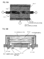
- FIGS. 18A, 18B , 19A and 19B are diagrams illustrating examples in which the capacitor element produced using the aerosol deposition process of the invention is employed, not in coiled electrolytic capacitors illustrated in FIG. 9 , but in multilayer and single-layer electrolytic capacitors.
- FIG. 18A is a schematic diagram illustrating the cross-sectional structure at the interior of a two-terminal unit capacitor element 600.
- a dielectric oxide film layer 700 is formed on both sides of an anode foil 521.
- An anode terminal 512 is connected to one end of the anode foil 521.
- a cathode foil 522 has a two-layer structure including a layer 522A containing metal particles and resin and a layer 522B containing carbon particles and resin. The cathode foil 522 having the two-layer structure is formed so as to surround one end and both sides of the anode foil 521.
- FIG. 18B is a cross-sectional view of an electrolytic capacitor in which the unit capacitor elements 600 of FIG. 18A are stacked.
- a housing 510A is formed of a insulating case, and the exposed anode foils 521 of stacked unit capacitor elements 600 are connected in common at one end to an anodic electrode terminal 512.
- the metal particle and resin-containing layers 522A of the stacked unit capacitor elements 600 are electrically connected in common to the cathode electrode terminal 513.
- FIG. 19A is a schematic diagram illustrating the cross-sectional structure at the interior of a three-terminal unit capacitor element 600.
- Dielectric oxide film layers 700 are formed on both sides of an anode foil 521.
- the anode foil 521 is connected at both ends thereof to anode terminals 512.
- a cathode foil 522 has a two-layer structure composed of a layer 522A containing metal particles and resin and a layer 522B containing carbon particles and resin. Cathode foils 522 having the two-layer structure are formed so as to surround the dielectric oxide film layers 700, with the anode foil 521 at the center.
- FIG. 19B is a cross-sectional view of an electrolytic capacitor in which the unit capacitor elements 600 of FIG. 19A are stacked.
- a housing 510B is formed of an electrically conductive metal case. Both ends of the anode foil 521 in the stacked unit capacitor elements 600 are connected in common to the respective anodic electrode terminals 512A and 512B.
- the cathodic electrode terminals 13 are electrically connected to the metal particle and resin-containing cathode foil layers 522A of the unit capacitor elements 600 through an electrically conductive resin 601 which fixes in place the stacked unit capacitor elements 600. By this means, the three-terminal type electrolytic capacitor is formed.
- Table 2 compares the effects that arise as a result of differences in the structure of the dielectric oxide film layer 700 in electrolytic capacitors that are formed using an anode foil 521 on which the above dielectric oxide film layer 700 according to the invention was formed.
- Aluminum foil (99%) having a thickness of 40 ⁇ m obtained by rolling was annealed at 300°C in an inert gas, thereby carrying out pretreatment.
- This foil was electrolytically treated for 8 minutes at a current density of 0.2 A/m 2 (50 Hz) in an aqueous solution of hydrochloric acid, nitric acid and AlCl 3 , thereby carrying out surface roughening treatment. Conversion treatment in an aqueous solution of ammonium adipate was subsequently carried out.
- the comparative example does not carry out the roughening treatment by film formation with fine particles of aluminum or fine particles of ceramic in Steps S2 to S7 of the treatment sequence in the fifth embodiment.
- the leakage current 30 minutes after a predetermined voltage of 20 V had been reached was measured for anode foil formed in each of the embodiments.
- the tensile strength of the film was also measured.
- the tensile strength at this time was measured by cutting out test pieces having a width of 1 cm and a length of 5 cm, and subjecting them to strain on a tensile testing machine at a test rate of 10 mm/min. If the strength at break was 1.5 kg/cm (not normalized by thickness; this value is specified based on the two-dimensional shape of the test piece) or more, the piece was rated as acceptable. In addition, the tensile strength of the film foil was measured.
- the electrostatic capacitance per unit surface area was the electrostatic capacitance measured in an aqueous solution of ammonium adipate.
- the tensile strengths of the foils of the sixth to eighth embodiments are higher than in Comparative Example 2.
- the electrostatic capacitance per unit surface area in the sixth to eighth embodiments was from 150 to 180 ⁇ F, which was about four times the value of 40 ⁇ F in Comparative Example 2.
- This invention thus makes it possible to provide electrolytic capacitors having an electrostatic capacitance about four times that of prior-art electrolytic capacitors.
- valve metal particles that are deposited may be adjusted after taking into consideration the relationship between the voltage resistance and capacitance of the films obtained by the aerosol deposition process, or a single type of valve metal may be deposited alone.
- the ultrafine particle ceramic of barium titanate used in these embodiments are subjected beforehand to 5 hours of heat treatment at 900°C. This enables a film structure having few impurities to be formed.
- the fine particles used in the aerosol deposition process it is preferable to subject the fine particles used in the aerosol deposition process to pretreatment, and more preferable to subject the fine particles to heat treatment at a temperature not less than the temperature at which the impurities decompose.
- Global fine particles produced by atomization are used in these embodiments as the powder of ultrafine particles of aluminum. It was possible in this way to achieve good deposition due to a large strain during an aerosol deposition process.
- the anode foil has an increased capacitance while retaining strength, it is possible to achieve an increased capacitance, both in a coiled electrolytic capacitor without breakage in the connections to the anodic and cathodic electrode metals, and also in a multilayer electrolytic capacitor without foil failure during stacking. Accordingly the present invention makes a significant contribution to the industry.
Landscapes
- Engineering & Computer Science (AREA)
- Power Engineering (AREA)
- Microelectronics & Electronic Packaging (AREA)
- Chemical & Material Sciences (AREA)
- Chemical Kinetics & Catalysis (AREA)
- Electrochemistry (AREA)
- Materials Engineering (AREA)
- Other Surface Treatments For Metallic Materials (AREA)
- Fixed Capacitors And Capacitor Manufacturing Machines (AREA)
- ing And Chemical Polishing (AREA)
Abstract
An electrode foil includes a structure in which metal particles and ceramic particles, which primarily include at least one of valve metal particles having a dielectric constant and ceramic particles, are deposited on a surface of a metal foil. The electrode foil is manufactured by placing an aluminum foil in a film-forming chamber of an aerosol chamber, aerosolizing aluminum powder, and spraying the aerosolized aluminum powder onto the aluminum foil placed in the film-forming chamber so as to deposit aluminum particles on the aluminum foil. Also, an electrolytic capacitor has the above electrode foil.
Description
- The present invention relates to an electrode foil suitable as the anode foil in an electrolytic capacitor, a method of manufacturing such an electrode foil, and an electrolytic capacitor.
- (A) Electrode Foils and Methods of Manufacture Thereof
Aluminum electrode foils for electrolytic capacitors are generally produced using as the starting material at least 98% high-purity aluminum that has been rendered into the form of a foil by rolling. Innumerable pits are formed on the surface of the aluminum foil using a known direct-current electrolytic etching process, an alternating-current electrolytic etching process, or both in alternation, within an acid or alkali solution that dissolves aluminum, thereby enlarging the actual surface area and increasing the electrostatic capacitance. - With such etching methods, a multiplicative effect per unit surface area of several hundred-fold, generally about 300 to 400 times, is achieved.
- An advantage of electrolytic capacitors is that, because the dielectric layer is composed of an extremely thin oxide film layer, the electrostatic capacitance per unit surface area of the electrode is high, enabling electrolytic capacitors which are small yet of large capacitance to be obtained. However, with the miniaturization of electronic devices, there exists a need for electrolytic capacitors of even smaller size and higher capacitance.
- When attempting to increase the capacitance per unit surface area by etching treatment as described above, the entire aluminum foil becomes filled with etching pits, which makes the electrode foil fragile and lowers the electrode foil strength.
- To address this problem, one method for achieving a large electrode foil surface area while maintaining the foil strength is to etch an aluminum foil of substantial thickness and thereby increase the capacitance per unit surface area.
- In this method, the capacitance per unit surface area is large, but when such an electrode foil is used to construct a common coiled electrolytic capacitor, the large thickness of the electrode foil places limits on the length of electrode foil that may be used, resulting in the formation of a capacitor element which will not fit within the case.
- In addition, in the case of multilayer solid electrolytic capacitors, due to height constraints resulting from the shape, it is hard to make the height too large. In forming the capacitors from a foil with reduced strength such as that mentioned above, it is hard to set the welding conditions for stacking, and problems with the strength after welding also arise.
- In thus trying to achieve a higher capacitance, the number of stacked layers may be increased or thick electrode foils may be used, resulting in an increase in the height of the capacitor.
- In addition to the general prior art mentioned above, in the case of coiled electrolytic capacitors, as described in
Patent Document 1, a method is known which, based on the fact that the capacitance is computed as the composite capacitance, increases the capacitance by forming a vapor-deposited film of metal nitride on a substrate surface. Also,Patent Document 2 discloses a method for achieving an increased capacitance by using foil which has been brought into physical contact with carbon as the cathode to cancel the cathode-side capacitance so that only the anode-side capacitance is reflected in the composite capacitance. - (B) Electrolytic Capacitors
Electrolytic capacitors are electronic components which are widely used in electronic devices, and generally have the following type of construction. - The action of having resistance to a voltage applied in one direction but losing such resistance when a voltage is applied in the opposite direction is called a "valve action." An electrolytic capacitor uses a valve metal (e.g., aluminum) having such a valve action as the anode. By means of treatment such as anodic oxidation, an insulating oxide film is formed on the anode surface.
- This oxide film acts as a dielectric layer; an electrolyte such as an electrolytic solution or an electrically conductive polymer, or a solid electrolyte, is in contact with the oxide film substantially as a cathode.
- In a coiled capacitor, the electrolyte is held by electrolytic paper (separator) or the like. In a flat-plate capacitor, a carbon paste and metal particles with a resin material are formed on the electrolyte in this order, resulting in a cathode layer.
- In each type of electrolytic capacitor, the cathode-side electrode is led out from a cathode made of a metal such as aluminum.
- The anode-side electrode and the cathode-side electrode are generally made of foils that have been cut into strips. In a coiled capacitor, the capacitor element is formed by winding the foils together with a separator.
In a flat-plate capacitor, the capacitor element is formed by arranging as an anode-side electrode, a cathode layer, and a cathode-side electrode or the like, all of which are of square shape. Stacking together a plurality of such capacitor elements results in a multilayer capacitor. - The cathode layer is connected to a lead-out electrode which is composed primarily of a metal and electrically connects the cathode layer to the exterior, and is thereby led out to the exterior from any of various types of housings which encase the capacitor element.
- Here, because the dielectric layer is composed of an extremely thin oxide film layer, the electrolytic capacitor is characterized by a high electrostatic capacitance per unit surface area of the electrode, enabling a small capacitor of large capacitance to be obtained. However, with the miniaturization of electronic devices, smaller sizes and larger capacitances are being demanded even of electrolytic capacitors.
- To increase the capacitance of electrolytic capacitors, enlargement of the surface area by using etching treatment or the like to roughen the electrode surface has hitherto been carried out. However, the surface area enlargement by such roughening has been approaching the limit recently, new measures for increasing the electrostatic capacitance are being sought.
- For example, by etching an aluminum foil to form countless small pits extending deeply into the inner portion of the aluminum foil in order to increase the capacitance per unit surface area, a larger capacitance per unit surface area may be achieved.
- However, when attempting to increase the capacitance per unit surface area in the above manner, the entire aluminum foil becomes filled with etching pits, which makes the electrode foil fragile and lowers the electrode foil strength.
- To address this problem, one method for achieving a large electrode foil surface area while maintaining the foil strength is to etch an aluminum foil of substantial thickness and thereby increase the capacitance per unit surface area. In this method, the capacitance per unit surface area is large, but when such an electrode foil is used to construct common coiled electrolytic capacitors, the large thickness of the electrode foil places limits on the length of electrode foil that may be used, resulting in the formation of a capacitor element which will not fit within the case.
- In addition, in the case of multilayer solid electrolytic capacitors, due to height constraints resulting from the shape, it is hard to make the height too large. In forming the capacitors from a foil with reduced strength such as that mentioned above, it is hard to set the welding conditions for stacking, and problems with the strength after welding also arise.
- In thus trying to increase a higher capacitance, the number of stacked layers may be increased or thick electrode foils may be used, resulting in an increase in the height of the capacitor.
- In addition to the general art mentioned above, in the case of coiled electrolytic capacitors, as described in
Patent Document 1, a method is known which, based on the fact that the capacitance is computed as the composite capacitance, increases the capacitance by forming a vapor-deposited film of metal nitride on a substrate surface. Also,Patent Document 2 discloses a method for achieving an increased capacitance by using foil which has been brought into physical contact with carbon as the cathode to cancel the cathode-side capacitance so that only the anode-side capacitance is reflected in the composite capacitance. Patent Document 1: Japanese Laid-open Patent Publication No.02-117123
Patent Document 2: Japanese Patent No.3,875,705 - (A) Electrode Foil and Method of Manufacture
However, even when these prior-art methods are used, in the absence of an anode material capable of achieving a large capacitance while retaining a thickness, strength and voltage resistance comparable to what exists today, it will not be possible to obtain an electrolytic capacitor capable of fully addressing the even larger capacitance that will be required henceforth by the market. - It is therefore a first object of the invention to provide an electrode foil structure which is suitable for an anode foil and is capable of dramatically increasing the anode foil surface area that relates to the capacitance of a capacitor while retaining a thickness, strength and voltage resistance comparable to the prior art, and to provide a method of manufacturing such an electrode foil.
- (B) Electrolytic Capacitor
As noted above, even when these prior-art methods are used, in the absence of an anode material capable of achieving a large capacitance while retaining a thickness, strength and voltage resistance comparable to what exists today, it will not be possible to obtain an electrolytic capacitor capable of fully addressing the even larger capacitance that will be required henceforth by the market. - Therefore, a second object of the invention is to provide an anodic electrode foil structure which dramatically increases the anode foil surface area that relates to the capacitance of a capacitor while retaining a thickness, strength and voltage resistance comparable to the prior art, and to provide a large-capacitance electrolytic capacitor which uses the same.
- (A) Electrode Foil and Method of Manufacture Thereof
To achieve the above first object, the electrode foil according to the present invention is characterized by having a structure in which metal particles and ceramic particles, which primarily include at least one of valve metal particles having a dielectric constant and ceramic particles, are deposited on a surface of a metal foil. - In addition, the electrode foil is characterized in that the deposit of the metal particles and/or ceramic particles is formed by using aerosol deposition.
- Also, to achieve the above first object, the method of manufacturing an electrode foil according to the present invention is characterized by placing an aluminum foil in a film-forming chamber of an aerosol chamber, aerosolizing aluminum powder, and spraying the aerosolized aluminum powder onto the aluminum foil placed in the film-forming chamber so as to deposit aluminum particles on the aluminum foil.
- Preferably, on the surface of aluminum foil or on the surface of etched foil obtained by electrolytically etching the surface of aluminum foil, by in this way uniformly diffusing an ultrafine powder having a dielectric constant in a high-velocity gas and spraying the gas onto a surface of metal foil or etched foil serving as the target so as to form a formed film of ultrafine powder, then individually etching the particles of the fine powder, compared with conventional etched foil composed of aluminum alone, the surface area of aluminum may be increased in foil of the same thickness.
- To achieve the above second object, a first aspect of the invention provides an electrolytic capacitor having an anode foil composed of a metal with a valve action, a cathode layer, and an electrolyte layer interposed between the anode foil and the cathode layer, the capacitor being characterized in that the anode foil has on a surface thereof a dielectric oxide film layer formed by using an aerosol deposition method to deposit particles having a dielectric constant.
- In this first aspect, as a preferred embodiment, the anode foil is a flat rolled aluminum foil or an aluminum foil having a rough, etched surface, and the particles having a dielectric constant in the layer deposited on the anode foil are valve metal particles composed primarily of valve metal.
- Also, in this first aspect, as a preferred embodiment, the particles having a dielectric constant in the layer deposited on the anode foil further contain ceramic particles composed primarily of a ceramic.
- In the present invention thus constituted, because the electrolytic capacitors may have a layer formed by depositing valve metal particles having a high dielectric constant on the anode foil by an aerosol deposition process, anode foil having a larger surface area per unit surface area of the anode foil than etched anode foils used in conventional electrolytic capacitors may be obtained.
- Therefore, an electrolytic capacitor in which such an anode foil is used as an anodic electrode has a high electrolytic capacitance compared with prior-art electrolytic capacitors, enabling a small, high-capacitance electrolytic capacitor to be obtained.
- By additionally etching the above layer of valve metal particles deposited by an aerosol deposition process and the above anode foil, it is possible to increase the surface area of the deposited layer and the anode foil, enabling the capacitance of the electrolytic capacitor to be made even higher. The anode foil may also be subjected to etching treatment prior to the particle deposition step by aerosol deposition as described above.
- By subjecting the treated electrode foil to conversion treatment at a suitable applied voltage, it is possible to ensure voltage resistance. Moreover, compared with conventional etched and conversion-treated foil, there is also the advantage that the thickness of the deposited layer of valve metal particles may be adjusted by adjusting the blowing velocity and blowing time in the aerosol deposition process, making it possible to adjust the capacitance.
- By employing anode foil fabricated by such a manufacturing process as the anode foil in coiled electrolytic capacitors, single-layer capacitors and multilayer capacitors, it is possible to achieve a larger capacitance in these capacitors.
-
-
FIG. 1 is a schematic view illustrating the structure of a coiled electrolytic capacitor serving as an embodiment in which an electrode foil according to the invention is employed as an anode foil. -
FIG. 2 is a flow chart illustrating the sequence of steps in a method of manufacturing an electrode foil in a first embodiment according to the invention. -
FIG. 3 is a schematic diagram of an exemplary aerosol deposition chamber configuration. -
FIG. 4 is a flow chart illustrating the sequence of steps in a method of manufacturing an electrode foil in a second embodiment according to the invention. -
FIG. 5A is a first diagram illustrating aluminum foil having a rough, pre-etched surface (etched surface). -
FIG. 5B is a second diagram illustrating aluminum foil having a rough, pre-etched surface (etched surface). -
FIG. 6 is a flow chart illustrating the sequence of steps in a method of manufacturing an electrode foil in a third embodiment according to the invention. -
FIG. 7 is a flow chart illustrating the sequence of steps in a method of manufacturing an electrode foil in a fourth embodiment according to the invention. -
FIG. 8 is a diagram illustrating a ceramic (barium titanate)-aluminum film formed on the top surface of an aluminum foil substrate according to the fourth embodiment. -
FIG. 9 is a schematic view illustrating the structure of a coiled electrolytic capacitor serving as an embodiment in which the invention is employed. -
FIG. 10 is a schematic view illustrating the cross-sectional structure of the coiled capacitor element inFIG. 9 . -
FIG. 11 is a diagram illustrating the sequence of steps in a method of forming a dielectric oxide film layer on the surface of an anode foil in a fifth embodiment. -
FIG. 12 is a schematic diagram of an exemplary aerosol deposition chamber configuration. -
FIG. 13A is a diagram illustrating etched aluminum foil having a rough, pre-etched surface. -
FIG. 13B is a schematic diagram illustrating a layer of deposited fine aluminum particles obtained by aerosol deposition. -
FIG. 14 is a flow chart illustrating the sequence of steps in a method of manufacturing an electrode foil in a sixth embodiment according to the invention. -
FIG. 15 is a flow chart illustrating the sequence of steps in a method of manufacturing an electrode foil in a seventh embodiment according to the invention. -
FIG. 16 is a flow chart illustrating the sequence of steps in a method of manufacturing an electrode foil in an eighth embodiment according to the invention. This diagram illustrates an eighth embodiment of a dielectric oxide film layer. -
FIG. 17A is a diagram illustrating a ceramic (barium titanate)-aluminum film formed by aerosol deposition on the rough surface of an aluminum foil substrate. -
FIG. 17B is a diagram illustrating etching treatment of the ceramic (barium titanate)-aluminum film ofFIG. 17A . -
FIG. 18A is a schematic diagram illustrating the cross-sectional structure at the interior of a two-terminal unit capacitor element. -
FIG. 18B is a cross-sectional view of an electrolytic capacitor in which the unit capacitor elements ofFIG. 18A are stacked. -
FIG. 19A is a schematic diagram illustrating the cross-sectional structure at the interior of a three-terminal unit capacitor element. -
FIG. 19B is a cross-sectional view of an electrolytic capacitor in which the unit capacitor elements ofFIG. 19A are stacked. - Embodiments of the present invention are described below in conjunction with the diagrams.
- (A) Electrode Foil and Method of Manufacture Thereof
FIG. 1 is a schematic view illustrating the structure of a coiled electrolytic capacitor serving as an embodiment in which an electrode foil according to the invention is employed as an anode foil. -
FIG. 1A illustrates the outside appearance of the capacitor, andFIG. 1B illustrates a perspective view to the interior with the housing (metal case) 10 removed. Ananodic electrode lead 12 and acathodic electrode lead 13 are fixed to a sealant (insulating resin) 11. - A
wound capacitor element 20 is fixed to the sealant (insulating resin) 11 within the housing (metal case) 10, and theanodic electrode lead 12 and thecathodic electrode lead 13 are electrically connected to, respectively, an anode foil 21 (which is an electrode foil according to the invention) and acathode foil 22. - The
anode foil 21 and thecathode foil 22 are cylindrically coiled withelectrolytic paper 23 as a separator therebetween, and the final ends of the foils are fixed withtape 24 to maintain the coiled state. - Electrolytic capacitors which use the electrode foil of the invention achieve a higher capacitance than electrolytic capacitors of prior-art construction which use an etched electrode foil obtained by electrolytically etching the aluminum foil intended for use as the anode foil.
- Also, the electrode foil according to the invention is characterized by having a structure obtained by uniformly dispersing in a high-velocity gas an ultrafine powder of metal having a particle size in a range of from 100 nm to 100 µm, an ultrafine powder including the above ultrafine powder of metal and/or an oxide, a nitride or a carbide having a high dielectric constant of 10 or more, or an ultrafine powder of valve metal that has been oxidized at the surface and has a particle size of 500 nm or less, and spraying the resulting gas onto the surface of the etched electrode foil serving as the target, so as to form a foremed film of the ultrafine powder on the surface of a prior-art metal foil or an etched metal foil obtained by etching a prior-art metal foil.
- The above valve metal particles include at least one from among valve metal aluminum and compounds thereof, titanium and compounds thereof, tantalum and compounds thereof, and niobium and compounds thereof.
- With the foregoing construction, compared with conventional etched electrode foil composed of aluminum foil alone, electrode foil in which the surface area of aluminum has been increased may be obtained in electrode foil of the same thickness. In addition, a formed film of ultrafine powder that has been formed on the surface of the etched electrode foil may be electrolytically etched.
- With such treatment, compared with conventional etched electrode foil composed of aluminum foil alone, by means of this invention, electrode foil in which the surface area of aluminum has been increased may be obtained in electrode foil of the same thickness.
- Owing to this characteristic constitution of electrode foil according to the present invention, by using the foil as an anode foil, it is possible to provide a electrolytic capacitor having a smaller size and a higher capacitance.
- The distinctive features of the electrode foil and the method of manufacture thereof according to the present invention are described in greater detail below based on the following embodiments.
- (An Embodiment in which a Film of Fine Aluminum Particles is Formed on Conventional Aluminum Foil)
FIG. 2 is a flow chart illustrating the sequence of steps in a method of manufacturing an electrode foil in a first embodiment according to the invention. Illustrations of the states corresponding to the treatment steps are illustrated on the left side of the flow chart. - Aluminum foil 21 (purity, 99%) having a thickness of 40 µm was prepared by rolling (Step S1: State I).
- Surface treatment on the
aluminum foil 21 thus prepared was carried out as follows in an aerosol deposition chamber.FIG. 3 is a schematic diagram of an exemplary aerosol deposition chamber configuration. - A film-forming
chamber 303 has astage 304 which is movable in the X and Y directions in the interior thereof. The rolledaluminum foil 21 prepared in Step S1 is affixed to the stage 304 (Step S2). - The interior of the film-forming
chamber 303 was evacuated using avacuum pump 306, thereby lowering the pressure beforehand to 10 Pa or below (Step S3). - In a separate operation, a starting
powder 300 composed primarily of a powder of aluminum, which is a valve metal, having an average particle size of 8 µm was placed in anaerosol generator 301A, ultrasound was applied to theentire aerosol generator 301A by anoscillator 301B, and degassing in vacuum was carried out for 30 minutes while heating at about 150°C, thereby effecting pretreatment in which moisture that had formed on the powder surface is removed (Step S4). - High-purity helium gas (gas pressure, 2 kg/cm2; gas flow rate, 10 L/min) 302 was introduced into the
aerosol generator 301A, and the pretreated startingpowder 300 was aerosolized (Step S5). - Next, this aerosol was passed through a pipe and delivered to the film-forming
chamber 303 by anozzle 305. Thenozzle 305 used was one having a helical groove formed on the inside. Spraying was carried out for 3 minutes from anozzle 305 having a helical groove on the inside toward the aluminum foil substrate 21 (Step S6). The pressure within the chamber at this time was fixed at 500 Pa. - The
aluminum film 201A, which was formed of fine particles of aluminum on the top surface of thealuminum foil substrate 21 by aerosol deposition in this way, had a thickness of 20 µm (State II: aerosol deposition with fine aluminum particles). - It is also possible to form an aluminum film on both sides of the
aluminum foil substrate 21 by the same procedure. - Next, annealing the deposited aluminum metal particle in an inert gas at 300°C, which is a temperature at or below the melting point of aluminum + 100°C, thereby carrying out sintering pretreatment in which the deposited aluminum metal particles are densified. This foil was electrolytically treated for 8 minutes in an aqueous solution of hydrochloric acid, nitric acid and AlCl3 at a current density of 0.2 A/m2 (50 Hz), thereby carrying out roughening treatment (etching) (Step S7). This etching treatment resulted in the formation of a
microcavity layer 201B (State III). - Next, conversion treatment was carried out in an aqueous solution of ammonium borate/ammonium adipate (Step S8).
- Such treatment enlarges the surface area by forming a
microcavity layer 201B, in addition thesurface 201C of themicrocavity layer 201B is oxidized by the conversion treatment in Step S8, resulting in the formation of a dielectricoxide film layer 200 having a large dielectric constant on the surface of the aluminum foil substrate 21 (State IV). - Hence, as illustrated by IV in
FIG. 2 , a structure, where metal particles are stacked with gaps which are smaller than the metal particles, is formed on the surface of the metal foil, making it possible to achieve a structure in which an oxide film is formed on the surface of the metal particles. - The leak current of the dielectric
oxide film layer 200, which was formed by the treatment process inFIG. 2 , was measured after an applied voltage had reached to predetermined voltage of 20 V and 30 minutes had passed thereafter. In addition, the tensile strength of the film was measured. - The tensile strength was measured by cutting out test pieces having a width of 1 cm and a length of 5 cm, and subjecting the test pieces to strain on a tensile testing machine at a test rate of 10 mm/min. If the strength at break was 1.5 kg/cm (not normalized by thickness; this value is specified based on the two-dimensional shape of the test piece) or more, the piece was rated as acceptable.
- (An Embodiment in which a Film of Fine Aluminum Particles is Formed on Etched Aluminum Foil)
FIG. 4 is a flow chart illustrating the sequence of steps in a method of manufacturing an electrode foil in a second embodiment according to the invention. In the first embodiment according to the flow chart inFIG. 2 above, an example was described in which 99%aluminum foil substrate 21 having a thickness of 40 µm obtained by rolling was used as the electrode foil. As a second embodiment, an etched aluminum foil with a rough surface (etched surface) 201 subjected beforehand to etching treatment as illustrated inFIG. 5A , which has also been used in the prior art, was used. - That is, 99% aluminum foil having a thickness of 40 µm obtained by rolling was annealed at 300°C in an inert gas, thereby carrying out pretreatment. This foil was electrolytically treated for 8 minutes at a current density of 0.2 A/m2 (50 Hz) in an aqueous solution of hydrochloric acid, nitric acid and AlCl3, thereby carrying out surface roughening treatment. In this way, an
aluminum foil 21 having the etchedsurface 201 illustrated in the aluminum foil cross-section inFIG. 5A was obtained (Step S1). - Next, the roughened aluminum foil was subjected to the treatments in Steps S2 to S8 in the same way as the treatment sequence in
FIG. 2 explained earlier for the first embodiment. However, the etching treatment in Step S7 ofFIG. 2 was omitted. - It is also possible to form an aluminum film on both sides of the foil by the above procedure.
-
FIG. 5B schematically illustrates the cross-section of alayer 202 obtained as described above using aerosol deposition to deposit fine particles of aluminum on arough surface 201 that was subjected to etching treatment beforehand. - As in the first embodiment, the leakage current 30 minutes after reaching a predetermined voltage of 20 V was measured.
The tensile strength was measured by cutting out test pieces having a width of 1 cm and a length of 5 cm, and subjecting them to strain on a tensile testing machine at a test rate of 10 mm/min. If the strength at break was 1.5 kg/cm (not normalized by thickness; this value is specified based on the two-dimensional shape of the test piece) or more, the piece was rated as acceptable. In addition, the tensile strength of the film foil was measured. - (An Embodiment in which a Film of Fine Ceramic Particles is Formed on Etched Aluminum Foil)
FIG. 6 is a flow chart illustrating the sequence of steps in a method of manufacturing an electrode foil in a third embodiment according to the invention. As in the second embodiment, 99% aluminum foil having a thickness of 40 µm obtained by rolling was annealed at 300°C in an inert gas, thereby carrying out pretreatment. This foil was electrolytically treated for 8 minutes at a current density of 0.2 A/m2 (50 Hz) in an aqueous solution of hydrochloric acid, nitric acid and AlCl3, thereby carrying out surface roughening treatment. In this way, an etchedaluminum foil 21 having the rough surface (etched surface) 201 inFIG. 5A was obtained (Step S1). - The etched aluminum foil 21 (see
FIG. 5A ) was subjected as described below to surface treatment in the aerosol deposition chamber illustrated inFIG. 2 in accordance with the flow inFIG. 6 . - The rolled
aluminum foil 21 prepared in Step S1 was affixed to astage 304 which is movable in the X and Y directions within the film-forming chamber 303 (Step S2). - The interior of the film-forming
chamber 303 was evacuated using avacuum pump 306, thereby lowering the pressure beforehand to 10 Pa or below (Step S3). - In a separate operation, ultrafine ceramic particles of barium titanate having an average particle size of 100 nm were placed in an
aerosol generator 301A as the startingpowder 300, ultrasound was applied to theentire aerosol generator 301A by anoscillator 301B, and degassing in vacuum was carried out for 30 minutes while heating at about 150°C, thereby effecting pretreatment in which moisture that had formed on the powder surface is removed (Step S4). - High-purity helium gas (gas pressure, 2 kg/cm2; gas flow rate, 10 L/min) 302 was introduced into the
aerosol generator 301A, and the pretreated startingpowder 300 was aerosolized (Step S5). - Next, this aerosol was passed through a pipe and delivered to the film-forming
chamber 303 by anozzle 305. Thenozzle 305 used was one having a helical groove formed on the inside. Spraying was carried out for 3 minutes from anozzle 305 having a helical groove on the inside toward the aluminum foil substrate 21 (Step S6). The pressure within the chamber at this time was fixed at 500 Pa. - The ceramic (barium titanate) film, which was formed of fine particles on the top surface of the
aluminum foil substrate 21 by aerosol deposition in this way, had a thickness of 2 µm. - It is also possible to form a ceramic film on both sides of the
aluminum foil substrate 21 by the same procedure. - Next, conversion treatment was carried out in an aqueous solution of ammonium adipate (Step S8).
- The etching treatment (Step S7) in
FIG. 2 was omitted in this third embodiment as well. - The dielectric
oxide film layer 200 formed by the above treatment steps illustrated inFIG. 6 was then subjected to leakage current measurement 30 minutes after reaching a predetermined voltage of 20 V. The tensile strength of the film was also measured. - Tensile strength measurement was performed by cutting out test pieces having a width of 1 cm and a length of 5 cm, and subjecting them to strain on a tensile testing machine at a test rate of 10 mm/min. If the strength at break was 1.5 kg/cm (not normalized by thickness; this value is specified based on the two-dimensional shape of the test piece) or more, the piece was rated as acceptable.
- (An Embodiment in which a Film of a Mixture of Fine Ceramic Particles and Fine Aluminum Particles is Formed on Etched Aluminum Foil)
FIG. 7 is a flow chart illustrating the sequence of steps in a method of manufacturing an electrode foil in a fourth embodiment according to the invention. As in the above second and third embodiments, 99% aluminum foil having a thickness of 40 µm obtained by rolling was annealed at 300°C in an inert gas, thereby carrying out pretreatment was carried out. This foil was electrolytically treated for 8 minutes at a current density of 0.2 A/m2 (50 Hz) in an aqueous solution of hydrochloric acid, nitric acid and AlCl3, thereby carrying out surface roughening treatment.
In this way, analuminum foil 21 having the etchedsurface 201 inFIG. 5A was obtained (Step S1). - The etched aluminum foil 21 (see
FIG. 5A ) was subjected as described below to surface treatment in the aerosol deposition chamber illustrated inFIG. 2 in accordance with the flow chart inFIG. 7 . - The rolled
aluminum foil 21 prepared in Step S1 was affixed to astage 304 which is movable in the X and Y directions within the film-forming chamber 303 (Step S2). - The interior of the film-forming
chamber 303 was evacuated using avacuum pump 306, thereby lowering the pressure beforehand to 10 Pa or below (Step S3). - In a separate operation, a mixture of ultrafine ceramic particles of barium titanate having an average particle size of 100 nm and ultrafine aluminum powder having an average particle size of 8 µm was placed in an
aerosol generator 301A as the startingpowder 300, ultrasound was applied to theentire aerosol generator 301A by anoscillator 301B, and degassing in vacuum was carried out for 30 minutes while heating at about 150°C, thereby effecting pretreatment in which moisture that had formed on the powder surface is removed (Step S4). - High-purity helium gas (gas pressure, 2 kg/cm2; gas flow rate, 10 L/min) 302 was introduced into the
aerosol generator 301A, and the pretreated startingpowder 300 was aerosolized (Step S5). - Next, this aerosol was passed through a pipe and delivered to the film-forming
chamber 303 by anozzle 305. Thenozzle 305 used was one having a helical groove formed on the inside. Spraying was carried out for 3 minutes from anozzle 305 having a helical groove on the inside toward the aluminum foil substrate 21 (Step S6). The pressure within the chamber at this time was fixed at 500 Pa. - In this way, the ceramic (barium titanate) -
aluminum film 200, which was formed of fine particles of ceramic 202a and fine particles ofaluminum 202b on the top surface of thealuminum foil substrate 21 by aerosol deposition as illustrated inFIG. 8 , had a thickness of 20 µm. - It is also possible to form a ceramic (barium titanate) - aluminum film on both sides of the
aluminum foil substrate 21 by the same procedure. - Next, conversion treatment was carried out in an aqueous solution of ammonium adipate (Step S8).
- The etching treatment (Step S7) in
FIG. 2 was omitted in this fourth embodiment as well. - The dielectric
oxide film layer 200 formed by the above treatment steps illustrated inFIG. 7 was then subjected to leakage current measurement 30 minutes after reaching a predetermined voltage of 20 V. The tensile strength of the film was also measured. - The tensile strength was measured by cutting out test pieces having a width of 1 cm and a length of 5 cm, and subjecting them to strain on a tensile testing machine at a test rate of 10 mm/min. If the strength at break was 1.5 kg/cm (not normalized by thickness; this value is specified based on the two-dimensional shape of the test piece) or more, the piece was rated as acceptable.
- A comparative example for comparison with the above first to fourth embodiments was carried out as follows.
- Aluminum foil (99%) having a thickness of 40 µm obtained by rolling was annealed at 300°C in an inert gas, thereby carrying out pretreatment. This foil was electrolytically treated for 8 minutes at a current density of 0.2 A/m2 (50 Hz) in an aqueous solution of hydrochloric acid, nitric acid and AlCl3, thereby carrying out surface roughening treatment. Next, conversion treatment in an aqueous solution of ammonium adipate was carried out.
- That is, in the comparative example, the roughening treatment by means of film formation with fine particles of aluminum or fine particles of ceramic, of Steps S2 to S7 in the treatment sequence of the first embodiment, was not carried out.
- The leakage current 30 minutes after reaching a predetermined voltage of 20 V was measured. In addition, the tensile strength of the film was measured.
- Tensile strength measurement was performed by cutting out test pieces having a width of 1 cm and a length of 5 cm, and subjecting them to strain on a tensile testing machine at a test rate of 10 mm/min. If the strength at break was 1.5 kg/cm (not normalized by thickness; this value is specified based on the two-dimensional shape of the test piece) or more, the piece was rated as acceptable. In addition, the tensile strength of the film was measured.
- Table 1 below is a table comparing the above first to fourth embodiments and the comparative example.
- In Table 1, the second to fourth embodiments, the foils of which are obtained by forming a deposited layer by the aerosol deposition method of the invention on a prior-art etched aluminum foil , are compared with the comparative example.
- The tensile strength of the foils in the first to fourth embodiments are higher than in the comparative example. The electrostatic capacitance per unit surface area in the second to fourth embodiments was from 150 to 180 µF, which was about four times the value of 40 µF in the comparative example.
- This invention thus makes it possible to provide electrolytic capacitors having an electrostatic capacitance about four times that of prior-art electrolytic capacitors.
- Another advantage is that the kind and mixing ratio of valve metal particles that are deposited may be adjusted after taking into consideration the relationship between the voltage resistance and capacitance of the films obtained by the aerosol deposition process. Of course, a single kind of valve metal may be deposited alone.
- The electrostatic capacitance per unit surface area was obtained by measuring the electrostatic capacitance in an aqueous solution of ammonium adipate.
-
Table 1. Comparison of Capacitance in Foil Alone Film structure Tensile strength (kg/cm) of foil after conversion treatment, 80 µm thick Leakage current 30 minutes after reaching 20 V (µA/5 cm2) Electrostatic capacitance (µF/cm2) Present invention First embodiment Aluminum aerosol deposition film on flat rolled aluminum foil 2.5 0.9 100 Second embodiment Aluminum aerosol deposition film on etched aluminum foil 2.0 1.1 150 Third embodiment Ceramic aerosol deposition film on etched aluminum foil 2.0 3.4 180 Fourth embodiment Ceramic and aluminum mixture aerosol deposition film on etched aluminum foil 2.0 2.5 165 Comparative example Comparative example Aluminum foil etched structure 1.5 1.0 40 - (B) Electrolytic Capacitor
FIG. 9 is a schematic view illustrating the structure of a coiled electrolytic capacitor serving as an embodiment in which the invention is employed. -
FIG. 9A illustrates the outside appearance of the capacitor, andFIG. 9B illustrates a perspective view to the interior with the housing (metal case) 510 removed. Ananodic electrode lead 512 and a cathodic electrode lead 513 are fixed to a sealant (insulating resin) 511. - A wound capacitor element 520 is fixed to the sealant (insulating resin) 511 within the housing (metal case) 510, and the
anodic electrode lead 512 and the cathodic electrode lead 513 are electrically connected to, respectively, ananode foil 521 and acathode foil 522. - The
anode foil 521 and thecathode foil 522 are cylindrically wound withelectrolytic paper 523 as a separator therebetween, and the final ends of the foils are fixed with tape 524 to maintain the coiled state. - The electrolytic capacitor of the invention achieves a higher capacitance than electrolytic capacitors of prior-art constructions which use an etched electrode foil obtained by electrolytically etching the aluminum foil intended for use as the anode foil.
- The inventive electrolytic capacitor is characterized by uniformly dispersing in a high-velocity gas an ultrafine powder of metal, or an ultrafine powder of metal in combination with an ultrafine powder having a high dielectric constant or an ultrafine powder of valve metal that has been oxidized at the surface, and spraying the resulting gas onto the surface of the etched electrode foil serving as the target so as to form a formed film of ultrafine powder.
- In this way, compared with prior-art etched electrode foil of aluminum foil alone, electrode foil in which the surface area of aluminum has been increased may be obtained in electrode foil of the same thickness. Moreover, a formed film of ultrafine powder that has been additionally formed on the surface of the etched electrode foil may be electrolytically etched.
- With such treatments, compared with a conventional etched electrode foil composed of aluminum foil alone, electrode foil in which the surface area of aluminum has been further enlarged may be employed in electrode foil of the same thickness.
- Owing to this characteristic constitution of the invention, it is possible to provide an electrolytic capacitor which is smaller in size and has a higher capacitance.
- The characteristics of the invention will be specifically described with reference to examples.
-
FIG. 10 is a schematic view illustrating the cross-sectional structure of the coiled capacitor element 520 inFIG. 9 . Theanode foil 521 and thecathode foil 522 are placed one over the another with anelectrolytic paper 530 impregnated with electrolyte 531 as the separator interposed therebetween. - The
cathode foil 522 may be constructed so as to include at least one from among electrolytic paper, carbon, metal foil, metal particles and electrically conductive resin. - In addition, an electrolytic solution obtained by dissolving an organic acid salt or an inorganic acid salt in a protic solution may be used as the electrolyte 531. Moreover, a solid electrolytic capacitor may be obtained by using, as specific examples of the electrolyte 531, at least one solid electrolyte from among polythiophene-type, polypyrrole-type and polyaniline-type conductive polymers, and TCNQ complex salts.
- Here, the electrolytic capacitor according to the invention has the characteristic in particular that a dielectric
oxide film layer 700 is formed on the surface of theanode foil 521. -
FIG. 11 is a diagram illustrating the sequence of steps in a forming method of a fifth embodiment of a dielectricoxide film layer 700 on the surface of ananode foil 521. Figures depicting the states corresponding to the treatment steps are illustrated on the left side of the flow chart. - Aluminum foil 521 (purity, 99%) having a thickness of 40 µm was prepared by rolling (Step S1: State I).
- Surface treatment on the
aluminum foil 521 thus prepared was carried out as follows in the aerosol deposition chamber.FIG. 12 is a schematic diagram of an exemplary aerosol deposition chamber configuration. - A film-forming
chamber 303 has astage 304 which is movable in the X and Y directions in the interior thereof. The rolledaluminum foil 521 prepared in Step S1 is affixed to the stage 304 (Step S2). - The interior of the film-forming
chamber 303 was evacuated using avacuum pump 306, thereby lowering the pressure beforehand to 10 Pa or below (Step S3). - In a separate operation, a starting
powder 300 composed primarily of a powder of aluminum, which is valve metal, having an average particle size of 8 µm was placed in anaerosol generator 301A, ultrasound was applied to theentire aerosol generator 301A by anoscillator 301B, and degassing in vacuum was carried out for 30 minutes while heating at about 150°C, thereby effecting pretreatment in which moisture that had formed on the powder surface is removed (Step S4). - High-purity helium gas (gas pressure, 2 kg/cm2; gas flow rate, 10 L/min) 302 was introduced into the
aerosol generator 301A, and the pretreated startingpowder 300 was aerosolized (Step S5). - Next, this aerosol was passed through a pipe and delivered to the film-forming
chamber 303 by anozzle 305. Thenozzle 305 used was one having a helical groove formed on the inside. Spraying was carried out for 3 minutes from anozzle 305 having a helical groove on the inside toward the aluminum foil substrate 521 (Step S6). The pressure within the chamber at this time was fixed at 500 Pa. - The
aluminum film 701A, which was formed of fine particles of aluminum on the top surface of thealuminum foil substrate 521 by aerosol deposition in this way, had a thickness of 20 µm (State II: aerosol deposition with fine aluminum particles). - It is also possible to form an aluminum film on both sides of the
aluminum foil substrate 521 by the same procedure. - Next, annealing the deposited aluminum metal particles in an inert gas at 300°C, which is a temperature at or below the melting point of aluminum + 100°C, thereby carrying out sintering pretreatment in which the deposited aluminum metal particles are densified. This foil was electrolytically treated for 8 minutes in an aqueous solution of hydrochloric acid, nitric acid and AlCl3 at a current density of 0.2 A/m2 (50 Hz), thereby carrying out roughening treatment (etching) (Step S7). This etching treatment resulted in the formation of a
microcavity layer 701B (State III). - Next, conversion treatment was carried out in an aqueous solution of ammonium borate/ammonium adipate (Step S8).
- Such treatment enlarges the surface area by forming a
microcavity layer 701B, in addition to which thesurface 701C of themicrocavity layer 701B is oxidized by conversion treatment in Step S8, resulting in the formation of a dielectricoxide film layer 700 having a large dielectric constant on the surface of the aluminum foil substrate 521 (State IV). - In the embodiment according to the flow chart in
FIG. 11 above, an example was described in which 99% aluminum foil substrate having a thickness of 40 µm obtained by rolling was used as theanode foil 521. In addition, as a sixth embodiment, an etched aluminum foil with a rough surface (etched surface) 701 subjected beforehand to etching treatment as illustrated inFIG. 13A , which has also been used in the prior art, may be used. -
FIG. 14 is a flow chart illustrating the sequence of steps in a method of manufacturing an electrode foil in a sixth embodiment according to the invention. - That is, 99% aluminum foil having a thickness of 40 µm obtained by rolling was annealed at 300°C in an inert gas, thereby carrying out pretreatment. This foil was electrolytically treated for 8 minutes at a current density of 0.2 A/m2 (50 Hz) in an aqueous solution of hydrochloric acid, nitric acid and AlCl3, thereby carrying out surface roughening treatment. In this way, an
aluminum foil 521 having the etchedsurface 701 illustrated in the aluminum foil cross-section inFIG. 13A was obtained (Step S1). - Next, the roughened aluminum foil was subjected to the treatments in Steps S2 to S8 in the same way as the treatment sequence in
FIG. 10 explained earlier for the fifth embodiment. However, the etching treatment in Step S7 ofFIG. 10 was omitted. - It is also possible to form an aluminum film on both sides of the etched aluminum foil by the above procedure.
-
FIG. 13B schematically illustrates the cross-section of alayer 702 obtained as described above using aerosol deposition to deposit fine particles of aluminum on therough surface 701 subjected to etching treatment beforehand. -
FIG. 15 is a flow chart illustrating the sequence of steps in a method of manufacturing an electrode foil in a seventh embodiment according to the invention. As in the sixth embodiment, 99% aluminum foil having a thickness of 40 µm obtained by rolling was annealed at 300°C in an inert gas, thereby carrying out pretreatment. This foil was electrolytically treated for 8 minutes at a current density of 0.2 A/m2 (50 Hz) in an aqueous solution of hydrochloric acid, nitric acid and AlCl3, thereby carrying out surface roughening treatment. In this way, an etchedaluminum foil 521 having the rough surface (etched surface) 701 inFIG. 13A was obtained (Step S1). - The etched aluminum foil 521 (see
FIG. 13A ) was subjected as described below to surface treatment in the aerosol deposition chamber illustrated inFIG. 12 in accordance with the flow chart inFIG. 15 . - The rolled
aluminum foil 521 prepared in Step S1 was affixed to astage 304 which is movable in the X and Y directions within the film-forming chamber 303 (Step S2). - The interior of the film-forming
chamber 303 was evacuated using avacuum pump 306, thereby lowering the pressure beforehand to 10 Pa or below (Step S3). - In a separate operation, ultrafine ceramic particles of barium titanate having an average particle size of 100 nm were placed in an
aerosol generator 301A as the startingpowder 300, ultrasound was applied to theentire aerosol generator 301A by anoscillator 301B, and degassing in vacuum was carried out for 30 minutes while heating at about 150°C, thereby effecting pretreatment in which moisture that had formed on the powder surface is removed (Step S4). - High-purity helium gas (gas pressure, 2 kg/cm2; gas flow rate, 10 L/min) 302 was introduced into the
aerosol generator 301A, and the pretreated startingpowder 300 was aerosolized (Step S5). - Next, this aerosol was passed through a pipe and delivered to the film-forming
chamber 303 by anozzle 305. Thenozzle 305 used was one having a helical groove formed on the inside. Spraying was carried out for 3 minutes from anozzle 305 having a helical groove on the inside toward the aluminum foil substrate 521 (Step S6). The pressure within the chamber at this time was fixed at 500 Pa. - The ceramic (barium titanate) film, which was formed of fine particles on the top surface of the
aluminum foil substrate 521 by aerosol deposition in this way, had a thickness of 2 µm. - It is also possible to form a ceramic film on both sides of the
aluminum foil substrate 521 by the same procedure. - Next, conversion treatment was carried out in an aqueous solution of ammonium adipate (Step S8).
- The etching treatment (Step S7) in
FIG. 10 was omitted in this seventh embodiment as well. -
FIG. 16 is a flow chart illustrating the sequence of steps in a method of manufacturing an electrode foil in an eighth embodiment according to the invention. As in the above sixth and seventh embodiments, 99% aluminum foil having a thickness of 40 µm obtained by rolling was annealed at 300°C in an inert gas, thereby carrying out pretreatment. This foil was electrolytically treated for 8 minutes at a current density of 0.2 A/m2 (50 Hz) in an aqueous solution of hydrochloric acid, nitric acid and AlCl3, thereby carrying out surface roughening treatment. In this way, an etchedaluminum foil 521 having therough surface 701 inFIG. 13A was obtained (Step S1). - The etched aluminum foil 521 (see
FIG. 13A ) was subjected as described below to surface treatment in the aerosol deposition chamber illustrated inFIG. 12 in accordance with the flow chart inFIG. 15 . - The rolled
aluminum foil 521 prepared in Step S1 was affixed to astage 304 which is movable in the X and Y directions within the film-forming chamber 303 (Step S2). - The interior of the film-forming
chamber 303 was evacuated using avacuum pump 306, thereby lowering the pressure beforehand to 10 Pa or below (Step S3). - In a separate operation, a mixture of ultrafine ceramic particles of barium titanate having an average particle size of 100 nm and an ultrafine aluminum powder having an average particle size of 8 µm was placed in an
aerosol generator 301A as the startingpowder 300, ultrasound was applied to theentire aerosol generator 301A by anoscillator 301B, and degassing in vacuum was carried out for 30 minutes while heating at about 150°C, thereby effecting pretreatment in which moisture that had formed on the powder surface is removed (Step S4). - High-purity helium gas (gas pressure, 2 kg/cm2; gas flow rate, 10 L/min) 302 was introduced into the
aerosol generator 301A, and the pretreated startingpowder 300 was aerosolized (Step S5). - Next, this aerosol was passed through a pipe and delivered to the film-forming
chamber 303 by anozzle 305. Thenozzle 305 used was one having a helical groove formed on the inside. Spraying was carried out for 3 minutes from anozzle 305 having a helical groove on the inside toward the aluminum foil substrate 521 (Step S6). The pressure within the chamber at this time was fixed at 500 Pa. - In this way, the ceramic (barium titanate) -
aluminum film 702, which was formed of fine particles of ceramic 702a and fine particles ofaluminum 702b on therough surface 701 of thealuminum foil substrate 521 by aerosol deposition as illustrated inFIG. 17A , had a thickness of 20 µm. - It is also possible to form a ceramic (barium titanate) ceramic - aluminum film on both sides of the
aluminum foil substrate 521 by the same procedure. - Conversion treatment was then carried out in an aqueous solution of ammonium adipate (Step S8).
- Next, by carrying out heat treatment followed by conversion treatment corresponding to Step S4 in
FIG. 11 , astrong anode foil 521 on the surface of which had been formed analuminum oxide layer 701B was formed, and a dielectricoxide film layer 700 was formed. The etching treatment (Step S7) inFIG. 11 was omitted in this eighth embodiment as well. - In the above embodiments, due to the
rough surface 701 that has been etched beforehand and the depositedlayer 702 of aluminum particles (valve metal particles 702a) and barium titanate particles (ceramic particles 702b) deposited thereon, a larger surface area is obtained, enabling the electrostatic capacitance to be enlarged as well. - Also, as illustrated in
FIG. 17B , by carrying out the etching treatment in Step S7 ofFIG. 11 and thereby etching interparticle regions and the particles having weak bond strengths in theaerosol deposition film 702, a porous aluminum structure may be obtained. - Here, particles which include at least one from among valve metal aluminum and compounds thereof, titanium and compounds thereof, tantalum and compounds thereof, and niobium and compounds thereof may be used as the
valve metal particles 702a. - Also, materials composed of an oxide, a nitride, or a carbide with a dielectric constant of at least 10 may be used as the
ceramic particles 702b, aside from barium titanate particles. -
FIGS. 18A, 18B ,19A and 19B are diagrams illustrating examples in which the capacitor element produced using the aerosol deposition process of the invention is employed, not in coiled electrolytic capacitors illustrated inFIG. 9 , but in multilayer and single-layer electrolytic capacitors. -
FIG. 18A is a schematic diagram illustrating the cross-sectional structure at the interior of a two-terminalunit capacitor element 600. - A dielectric
oxide film layer 700 is formed on both sides of ananode foil 521. Ananode terminal 512 is connected to one end of theanode foil 521. Acathode foil 522 has a two-layer structure including a layer 522A containing metal particles and resin and a layer 522B containing carbon particles and resin. Thecathode foil 522 having the two-layer structure is formed so as to surround one end and both sides of theanode foil 521. -
FIG. 18B is a cross-sectional view of an electrolytic capacitor in which theunit capacitor elements 600 ofFIG. 18A are stacked. A housing 510A is formed of a insulating case, and the exposed anode foils 521 of stackedunit capacitor elements 600 are connected in common at one end to ananodic electrode terminal 512. - The metal particle and resin-containing layers 522A of the stacked
unit capacitor elements 600 are electrically connected in common to the cathode electrode terminal 513. - In this way, an electrolytic capacitor having a two-terminal construction is formed.
-
FIG. 19A is a schematic diagram illustrating the cross-sectional structure at the interior of a three-terminalunit capacitor element 600. - Dielectric oxide film layers 700 are formed on both sides of an
anode foil 521. Theanode foil 521 is connected at both ends thereof toanode terminals 512. Acathode foil 522 has a two-layer structure composed of a layer 522A containing metal particles and resin and a layer 522B containing carbon particles and resin. Cathode foils 522 having the two-layer structure are formed so as to surround the dielectric oxide film layers 700, with theanode foil 521 at the center. -
FIG. 19B is a cross-sectional view of an electrolytic capacitor in which theunit capacitor elements 600 ofFIG. 19A are stacked. A housing 510B is formed of an electrically conductive metal case. Both ends of theanode foil 521 in the stackedunit capacitor elements 600 are connected in common to the respective anodic electrode terminals 512A and 512B. - The
cathodic electrode terminals 13 are electrically connected to the metal particle and resin-containing cathode foil layers 522A of theunit capacitor elements 600 through an electricallyconductive resin 601 which fixes in place the stackedunit capacitor elements 600. By this means, the three-terminal type electrolytic capacitor is formed. - Table 2 compares the effects that arise as a result of differences in the structure of the dielectric
oxide film layer 700 in electrolytic capacitors that are formed using ananode foil 521 on which the above dielectricoxide film layer 700 according to the invention was formed. - In Table 2 below, a comparative example for the above fifth to eighth embodiments was carried as follows.
- Aluminum foil (99%) having a thickness of 40 µm obtained by rolling was annealed at 300°C in an inert gas, thereby carrying out pretreatment. This foil was electrolytically treated for 8 minutes at a current density of 0.2 A/m2 (50 Hz) in an aqueous solution of hydrochloric acid, nitric acid and AlCl3, thereby carrying out surface roughening treatment. Conversion treatment in an aqueous solution of ammonium adipate was subsequently carried out.
- That is, the comparative example does not carry out the roughening treatment by film formation with fine particles of aluminum or fine particles of ceramic in Steps S2 to S7 of the treatment sequence in the fifth embodiment.
- In addition, the leakage current 30 minutes after a predetermined voltage of 20 V had been reached was measured for anode foil formed in each of the embodiments. The tensile strength of the film was also measured.
- The tensile strength at this time was measured by cutting out test pieces having a width of 1 cm and a length of 5 cm, and subjecting them to strain on a tensile testing machine at a test rate of 10 mm/min. If the strength at break was 1.5 kg/cm (not normalized by thickness; this value is specified based on the two-dimensional shape of the test piece) or more, the piece was rated as acceptable. In addition, the tensile strength of the film foil was measured.
- The electrostatic capacitance per unit surface area was the electrostatic capacitance measured in an aqueous solution of ammonium adipate.
-
Table 2. Comparison of Capacitance in Foil Alone Film structure Tensile strength (kg/cm) of foil after conversion treatment, 80 µm thick Leakage current 30 minutes after reaching 20 V (µA/5 cm2) Electrostatic capacitance (µF/cm2) Present invention Fifth embodiment Aluminum aerosol deposition film on flat rolled aluminum foil 2.5 0.9 100 Sixth embodiment Aluminum aerosol deposition film on etched aluminum foil 2.0 1.1 150 Seventh embodiment Ceramic aerosol deposition film on etched aluminum foil 2.0 3.4 180 Eighth embodiment Ceramic and aluminum mixture aerosol deposition film on etched aluminum foil 2.0 2.5 165 Comparative example Comparative Example 2 Aluminum foil etched structure 1.5 1.0 40 - In above Table 2, the tensile strengths of the foils of the sixth to eighth embodiments are higher than in Comparative Example 2. The electrostatic capacitance per unit surface area in the sixth to eighth embodiments was from 150 to 180 µF, which was about four times the value of 40 µF in Comparative Example 2.
- This invention thus makes it possible to provide electrolytic capacitors having an electrostatic capacitance about four times that of prior-art electrolytic capacitors.
- Another advantage is that the kind and mixing ratio of valve metal particles that are deposited may be adjusted after taking into consideration the relationship between the voltage resistance and capacitance of the films obtained by the aerosol deposition process, or a single type of valve metal may be deposited alone.
- The ultrafine particle ceramic of barium titanate used in these embodiments are subjected beforehand to 5 hours of heat treatment at 900°C. This enables a film structure having few impurities to be formed.
- Hence, it is preferable to subject the fine particles used in the aerosol deposition process to pretreatment, and more preferable to subject the fine particles to heat treatment at a temperature not less than the temperature at which the impurities decompose.
- Global fine particles produced by atomization are used in these embodiments as the powder of ultrafine particles of aluminum. It was possible in this way to achieve good deposition due to a large strain during an aerosol deposition process.
- Accordingly, by using global fine particles having a particle shape that is nearly spherical, a film structure that is both dense and porous may be achieved.
- In the electrolytic capacitor according to the present invention, because the anode foil has an increased capacitance while retaining strength, it is possible to achieve an increased capacitance, both in a coiled electrolytic capacitor without breakage in the connections to the anodic and cathodic electrode metals, and also in a multilayer electrolytic capacitor without foil failure during stacking. Accordingly the present invention makes a significant contribution to the industry.
Claims (27)
- An electrode foil comprising a structure in which metal particles and ceramic particles, which primarily include at least one of valve metal particles having a dielectric constant and ceramic particles, are deposited on a surface of a metal foil.
- The electrode foil according to claim 1, wherein at least one of the metal particles and the ceramic particles are deposited using aerosol deposition.
- The electrode foil according to claim 1, wherein the metal particles have a particle size in a range of from 100 nm to 100 µm.
- The electrode foil according to claim 1, wherein the ceramic particles are composed of an oxide, a nitride, or a carbide; the oxide, the nitride, and the carbide have a dielectric constant of 10 or more.
- The electrode foil according to claim 1, wherein the ceramic particles have a particle size of 500 nm or less.
- The electrode foil according to claim 1, wherein the valve metal particles include at least one from among valve metal aluminum and compounds thereof, titanium and compounds thereof, tantalum and compounds thereof, and niobium and compounds thereof.
- A method for manufacturing an electrode foil, comprising:placing an aluminum foil in a film-forming chamber of an aerosol chamber;aerosolizing aluminum powder; andspraying the aerosolized aluminum powder onto the aluminum foil placed in the film-forming chamber so as to deposit aluminum particles on the aluminum foil.
- The method for manufacturing an electrode foil according to claim 7, wherein a surface of the aluminum foil placed in the film-forming chamber is roughened by electrolytic etching treatment.
- The method for manufacturing an electrode foil according to claim 7 or 8, wherein a surface of the aluminum foil on which the aluminum particles have been deposited is subjected to etching treatment.
- The method for manufacturing an electrode foil according to claim 9, wherein the surface on which the aluminum particles have been deposited and which has been subjected to the etching treatment is further subjected to conversion treatment.
- A method for manufacturing an electrode foil, comprising:placing an aluminum foil, a surface of which is subjected to etching treatment, in a film-forming chamber of an aerosol chamber;aerosolizing ceramic powder; andspraying the aerosolized ceramic powder onto the aluminum foil placed in the film-forming chamber so as to deposit ceramic particles on the aluminum foil.
- A method for manufacturing an electrode foil, comprising:placing an aluminum foil, a surface of which is subjected to etching treatment, in a film-forming chamber of an aerosol chamber;aerosolizing a mixture of aluminum powder and ceramic powder; andspraying the aerosolized mixture of the aluminum powder and the ceramic powder onto the aluminum foil placed in the film-forming chamber so as to deposit aluminum particles and ceramic particles on the aluminum foil.
- An electrolytic capacitor comprising:an anode foil composed of a metal with a valve action, a cathode layer, and an electrolyte layer interposed between the anode foil and the cathode layer,wherein the anode foil has on a surface thereof a dielectric oxide film layer formed by depositing particles having a dielectric constant.
- The electrolytic capacitor according to claim 13,
wherein the dielectric oxide film layer formed by depositing particles having a dielectric constant is formed using an aerosol deposition process. - The electrolytic capacitor according to claim 13 or 14,
wherein the anode foil is a flat rolled aluminum foil or an aluminum foil having a rough, etched surface; and the particles having a dielectric constant in layer deposited on the anode foil are valve metal particles composed primarily of a valve metal. - The electrolytic capacitor according to claim 15,
wherein the particles having a dielectric constant in the layer deposited on the anode foil further contain ceramic particles composed of primarily a ceramic. - The electrolytic capacitor according to claim 16,
wherein the ceramic particles are composed of an oxide, a nitride or a carbide; the oxide, the nitride, and the carbide have a dielectric constant of 10 or more. - The electrolytic capacitor according to claim 15,
wherein the valve metal includes at least one from among valve metal aluminum and compounds thereof, titanium and compounds thereof, tantalum and compounds thereof, and niobium and compounds thereof. - The electrolytic capacitor according to claim 15 or 16,
wherein the anode foil and the layer deposited are subjected to conversion treatment so as to form a metal oxide layer. - The electrolytic capacitor according to claim 13 or 14,
wherein an electrolyte of the electrolyte layer is an electrolyte solution prepared by dissolving an organic acid salt or an inorganic acid salt in a protic solvent. - The electrolytic capacitor of claim 13 or 14, wherein at least one solid electrolyte from among polythiophene-type polymer, polypyrrole-type polymer, polyaniline-type conductive polymers, and TCNQ complex salts is used as the electrolyte in the electrolyte layer.
- The electrolytic capacitor of claim 13 or 14, wherein the cathode layer includes at least any one of electrolytic paper, carbon, metal foil, metal particles and conductive resins.
- The electrolytic capacitor of claim 15, wherein the valve metal particles have a particle size in a range of from 100 nm to 100 µm.
- The electrolytic capacitor of claim 16, wherein the ceramic particles have a particle size of 500 nm or less.
- An electrode foil for use in a capacitor, comprising a layer formed by depositing metal particles on a metal foil surface, wherein metal particles are deposited so as to have small gaps therebetween; and
the metal particles are surface treated. - The electrode foil according to claim 25, wherein an oxide film is formed by the surface treatment.
- A capacitor which uses the electrode foil of claim 25.
Applications Claiming Priority (3)
| Application Number | Priority Date | Filing Date | Title |
|---|---|---|---|
| JP2007111570A JP5104008B2 (en) | 2007-04-20 | 2007-04-20 | Electrolytic capacitor |
| JP2007111569A JP5104007B2 (en) | 2007-04-20 | 2007-04-20 | Electrode foil and manufacturing method thereof |
| PCT/JP2008/001035 WO2008132829A1 (en) | 2007-04-20 | 2008-04-18 | Electrode foil, process for producing the electrode foil, and electrolytic capacitor |
Publications (1)
| Publication Number | Publication Date |
|---|---|
| EP2148341A1 true EP2148341A1 (en) | 2010-01-27 |
Family
ID=39925300
Family Applications (1)
| Application Number | Title | Priority Date | Filing Date |
|---|---|---|---|
| EP08751579A Withdrawn EP2148341A1 (en) | 2007-04-20 | 2008-04-18 | Electrode foil, process for producing the electrode foil, and electrolytic capacitor |
Country Status (5)
| Country | Link |
|---|---|
| US (2) | US8213159B2 (en) |
| EP (1) | EP2148341A1 (en) |
| KR (1) | KR101120872B1 (en) |
| CN (1) | CN101689429B (en) |
| WO (1) | WO2008132829A1 (en) |
Cited By (3)
| Publication number | Priority date | Publication date | Assignee | Title |
|---|---|---|---|---|
| CN102568858A (en) * | 2012-01-13 | 2012-07-11 | 西安交通大学 | Production method of high dielectric constant composite alumina film |
| EP2365496A4 (en) * | 2008-12-01 | 2013-01-23 | Panasonic Corp | ELECTRODE SHEET FOR CAPACITOR, AND L ELECTROLYTIC CAPACITOR USING THE SAME |
| US8659875B2 (en) | 2009-04-08 | 2014-02-25 | Panasonic Corporation | Capacitor and manufacturing method therefor |
Families Citing this family (23)
| Publication number | Priority date | Publication date | Assignee | Title |
|---|---|---|---|---|
| JP4978509B2 (en) * | 2008-02-22 | 2012-07-18 | 富士通株式会社 | Manufacturing method of electrode foil |
| CN102017034B (en) * | 2008-04-22 | 2016-01-27 | 东洋铝株式会社 | Electrode material for aluminum electrolytic capacitor and method of manufacturing same |
| JP2011029449A (en) * | 2009-07-27 | 2011-02-10 | Sanyo Electric Co Ltd | Capacitor electrode, method of manufacturing the same, and capacitor |
| CN102549692B (en) * | 2009-10-09 | 2013-09-18 | 松下电器产业株式会社 | Electrode foil and capacitor employing same |
| US20120261162A1 (en) * | 2010-04-07 | 2012-10-18 | Toyo Aluminium Kabushiki Kaisha | Method for manufacturing electrode structure, electrode structure, and capacitor |
| WO2012161158A1 (en) | 2011-05-26 | 2012-11-29 | 東洋アルミニウム株式会社 | Electrode material for aluminum electrolytic capacitor, and process for producing same |
| JP5769528B2 (en) | 2011-07-15 | 2015-08-26 | 東洋アルミニウム株式会社 | Electrode material for aluminum electrolytic capacitor and method for producing the same |
| TWI435352B (en) * | 2011-09-21 | 2014-04-21 | Apaq Technology Co Ltd | Aluminum foil having high specific surface area and manufacturing method thereof |
| CN103137331B (en) * | 2011-11-24 | 2016-01-27 | 至美电器股份有限公司 | Solid electrolytic capacitor core and capacitor |
| KR102079032B1 (en) | 2012-02-10 | 2020-02-19 | 도요 알루미늄 가부시키가이샤 | Method for manufacturing electrode material for aluminium electrolytic capacitor |
| US9123468B2 (en) * | 2013-03-14 | 2015-09-01 | Apaq Technology Co., Ltd. | Method for fabricating solid electrolytic capacitors |
| ITBO20130271A1 (en) * | 2013-05-29 | 2014-11-30 | Spal Automotive Srl | ELECTRIC MACHINE. |
| CN107077967A (en) * | 2014-08-26 | 2017-08-18 | 株式会社村田制作所 | Capacitor and its production technology |
| US10090112B2 (en) * | 2016-01-15 | 2018-10-02 | Pacesetter, Inc. | Use of etch resist masked anode frame for facilitation of laser cutting, particle and leakage current reduction |
| CN106847511B (en) * | 2017-02-14 | 2018-11-23 | 中国科学院合肥物质科学研究院 | A kind of high-ratio surface tantalum capacitor anodes tantalum foil and preparation method thereof |
| CN115050579A (en) * | 2017-03-31 | 2022-09-13 | 日本贵弥功株式会社 | Electrode foil and method for manufacturing the same, and winding type capacitor and method for manufacturing the same |
| JP1595451S (en) * | 2017-06-20 | 2018-01-22 | ||
| CN108666139A (en) * | 2018-03-30 | 2018-10-16 | 益阳艾华富贤电子有限公司 | Anode foils and aluminium electrolutic capacitor production method |
| CN109599269A (en) * | 2018-11-30 | 2019-04-09 | 南通海星电子股份有限公司 | The manufacturing method of surface mount electrode foil for aluminum electrolytic capacitors |
| CN112164588A (en) * | 2020-10-08 | 2021-01-01 | 实德电气有限公司 | Production process of intelligent capacitor |
| CN116670793A (en) * | 2020-12-28 | 2023-08-29 | 松下知识产权经营株式会社 | electrolytic capacitor |
| CN115172059B (en) * | 2022-08-09 | 2024-09-24 | 西安稀有金属材料研究院有限公司 | Method for preparing anode foil of aluminum electrolytic capacitor by combining aerosol spraying method |
| CN115172060A (en) * | 2022-08-30 | 2022-10-11 | 西安稀有金属材料研究院有限公司 | Method for preparing aluminum electrolytic capacitor anode foil based on electrophoretic deposition |
Family Cites Families (27)
| Publication number | Priority date | Publication date | Assignee | Title |
|---|---|---|---|---|
| JPH061751B2 (en) * | 1985-07-12 | 1994-01-05 | 昭和アルミニウム株式会社 | Anode material for electrolytic capacitors |
| JP2696882B2 (en) | 1988-02-19 | 1998-01-14 | 松下電器産業株式会社 | Manufacturing method of electrode foil for aluminum electrolytic capacitor |
| JPH02117123A (en) | 1988-10-27 | 1990-05-01 | Elna Co Ltd | Cathode material for electrolyte condenser |
| JP2696603B2 (en) * | 1990-11-21 | 1998-01-14 | 日立エーアイシー株式会社 | Manufacturing method of tantalum solid electrolytic capacitor |
| JP3280667B2 (en) * | 1990-11-21 | 2002-05-13 | 触媒化成工業株式会社 | Coating liquid for forming transparent conductive film, method for producing the same, conductive substrate, method for producing the same, and display device provided with transparent conductive substrate |
| JPH0785459B2 (en) | 1991-01-31 | 1995-09-13 | 太陽誘電株式会社 | Grain boundary insulation type semiconductor ceramic capacitor |
| JPH0864481A (en) | 1994-08-24 | 1996-03-08 | Matsushita Electric Ind Co Ltd | Electrode foil for electrolytic capacitor and manufacturing method thereof |
| JPH08167543A (en) | 1994-12-12 | 1996-06-25 | Matsushita Electric Ind Co Ltd | Aluminum electrode foil for electrolytic capacitor and manufacturing method thereof |
| WO1999065043A1 (en) * | 1998-06-09 | 1999-12-16 | Showa Denko K.K. | Solid electrolytic capacitor electrode foil, method of producing it and solid electrolytic capacitor |
| WO2001020625A1 (en) * | 1999-09-10 | 2001-03-22 | Matsushita Electric Industrial Co., Ltd. | Solid electrolytic capacitor and production method thereof, and conductive polymer polymerizing oxidizing agent solution |
| WO2002063645A1 (en) * | 2001-02-08 | 2002-08-15 | Showa Denko K.K. | Method for producing aluminum foil for capacitor and solid electrolytic capacitor |
| US6562652B2 (en) * | 2001-06-06 | 2003-05-13 | Kemet Electronics Corporation | Edge formation process with anodizing for aluminum solid electrolytic capacitor |
| IL143780A (en) | 2001-06-14 | 2007-06-03 | Cerel Ceramic Technologies Ltd | Process for manufacturing electrode |
| IL153289A (en) | 2002-12-05 | 2010-06-16 | Acktar Ltd | Electrodes for electrolytic capacitors and method for producing them |
| JP4383204B2 (en) * | 2003-03-31 | 2009-12-16 | 三洋電機株式会社 | Solid electrolytic capacitor and manufacturing method thereof |
| JP2005082835A (en) * | 2003-09-05 | 2005-03-31 | Honda Motor Co Ltd | Electrode plate for electrolysis, electrolysis apparatus, electrode plate unit, and method for electrolysis of hydrogen-containing compound |
| JP4491214B2 (en) | 2003-09-29 | 2010-06-30 | 富士通株式会社 | Capacitor element |
| US20050205879A1 (en) * | 2004-03-17 | 2005-09-22 | Fuji Photo Film Co., Ltd. | Photoelectric converting film stack type solid-state image pickup device |
| IL161606A0 (en) * | 2004-04-25 | 2004-09-27 | Acktar Ltd | Integral separator for electrolytic capacitors |
| JP3875705B2 (en) | 2004-09-22 | 2007-01-31 | 富士通メディアデバイス株式会社 | Solid electrolytic capacitor and manufacturing method thereof |
| JP2006108160A (en) * | 2004-09-30 | 2006-04-20 | Nippon Chemicon Corp | Solid electrolytic capacitor |
| WO2006038740A1 (en) * | 2004-10-08 | 2006-04-13 | Showa Denko K.K. | Electrode sheet for capacitors, method of manufacturing the same, and electrolytic capacitor |
| JP4572649B2 (en) | 2004-10-12 | 2010-11-04 | パナソニック株式会社 | Method for producing electrode foil for electrolytic capacitor |
| JP2007019233A (en) * | 2005-07-07 | 2007-01-25 | Fujitsu Media Device Kk | Stacked solid electrolytic capacitor |
| JP4587996B2 (en) * | 2005-11-22 | 2010-11-24 | 佐賀三洋工業株式会社 | Electrolytic capacitor |
| JP5263915B2 (en) | 2006-07-05 | 2013-08-14 | 富士通株式会社 | Capacitor element manufacturing method |
| JP4882567B2 (en) * | 2006-07-19 | 2012-02-22 | パナソニック株式会社 | Solid electrolytic capacitor manufacturing method and solid electrolytic capacitor |
-
2008
- 2008-04-18 WO PCT/JP2008/001035 patent/WO2008132829A1/en not_active Ceased
- 2008-04-18 CN CN2008800128544A patent/CN101689429B/en not_active Expired - Fee Related
- 2008-04-18 EP EP08751579A patent/EP2148341A1/en not_active Withdrawn
- 2008-04-18 KR KR1020097021814A patent/KR101120872B1/en not_active Expired - Fee Related
-
2009
- 2009-10-16 US US12/580,708 patent/US8213159B2/en not_active Expired - Fee Related
-
2012
- 2012-05-31 US US13/485,344 patent/US20120300371A1/en not_active Abandoned
Non-Patent Citations (1)
| Title |
|---|
| See references of WO2008132829A1 * |
Cited By (5)
| Publication number | Priority date | Publication date | Assignee | Title |
|---|---|---|---|---|
| EP2365496A4 (en) * | 2008-12-01 | 2013-01-23 | Panasonic Corp | ELECTRODE SHEET FOR CAPACITOR, AND L ELECTROLYTIC CAPACITOR USING THE SAME |
| US8659876B2 (en) | 2008-12-01 | 2014-02-25 | Panasonic Corporation | Electrode foil for capacitor and electrolytic capacitor using the electrode foil |
| US8659875B2 (en) | 2009-04-08 | 2014-02-25 | Panasonic Corporation | Capacitor and manufacturing method therefor |
| CN102568858A (en) * | 2012-01-13 | 2012-07-11 | 西安交通大学 | Production method of high dielectric constant composite alumina film |
| CN102568858B (en) * | 2012-01-13 | 2013-11-06 | 西安交通大学 | Production method of high dielectric constant composite alumina film |
Also Published As
| Publication number | Publication date |
|---|---|
| US8213159B2 (en) | 2012-07-03 |
| CN101689429B (en) | 2013-05-08 |
| WO2008132829A1 (en) | 2008-11-06 |
| KR20090122301A (en) | 2009-11-26 |
| KR101120872B1 (en) | 2012-02-27 |
| CN101689429A (en) | 2010-03-31 |
| US20100165544A1 (en) | 2010-07-01 |
| US20120300371A1 (en) | 2012-11-29 |
Similar Documents
| Publication | Publication Date | Title |
|---|---|---|
| US8213159B2 (en) | Electrode foil, method of manufacturing electrode foil, and electrolytic capacitor | |
| US6771488B2 (en) | Solid electrolytic capacitor and method of manufacturing the capacitor | |
| US6775127B2 (en) | Anode member for a solid electrolytic capacitor, method of producing the same and solid electrolytic capacitor using the same | |
| US9287055B2 (en) | Solid electrolytic capacitor and method for manufacturing same | |
| US8404134B2 (en) | Method for manufacturing electrode foil | |
| EP1592029B1 (en) | Production method for the capacitor | |
| EP2261933A1 (en) | Capacitor and method for manufacturing the same | |
| US20250232924A1 (en) | Electrolytic capacitor and production method therefor | |
| JP2017103412A (en) | Solid electrolytic capacitor | |
| JP5104008B2 (en) | Electrolytic capacitor | |
| US20180114647A1 (en) | Capacitor and method for manufacturing the capacitor | |
| CN114946000A (en) | Electrolytic capacitor and method for manufacturing electrolytic capacitor | |
| JP4285523B2 (en) | Electrode foil for solid electrolytic capacitor and manufacturing method thereof | |
| JP2002353068A (en) | Multilayer capacitor and method of manufacturing the same | |
| JP5104007B2 (en) | Electrode foil and manufacturing method thereof | |
| US20080047116A1 (en) | Method of producing electrolytic capacitor | |
| JPH06168855A (en) | Multilayer solid electrolytic capacitor and fabrication thereof | |
| JP4665854B2 (en) | Valve metal composite electrode foil and manufacturing method thereof | |
| US3675086A (en) | Electrical element laminated in structure | |
| JPH0785461B2 (en) | Capacitor | |
| JP3538309B2 (en) | Manufacturing method of multilayer ceramic electronic component | |
| JP4329800B2 (en) | Solid electrolytic capacitor and manufacturing method thereof | |
| JP3316896B2 (en) | Capacitor | |
| JPH0917686A (en) | Capacitor | |
| JPH04212405A (en) | Manufacture of ceramic electronic parts |
Legal Events
| Date | Code | Title | Description |
|---|---|---|---|
| PUAI | Public reference made under article 153(3) epc to a published international application that has entered the european phase |
Free format text: ORIGINAL CODE: 0009012 |
|
| 17P | Request for examination filed |
Effective date: 20091109 |
|
| AK | Designated contracting states |
Kind code of ref document: A1 Designated state(s): AT BE BG CH CY CZ DE DK EE ES FI FR GB GR HR HU IE IS IT LI LT LU LV MC MT NL NO PL PT RO SE SI SK TR |
|
| AX | Request for extension of the european patent |
Extension state: AL BA MK RS |
|
| DAX | Request for extension of the european patent (deleted) | ||
| STAA | Information on the status of an ep patent application or granted ep patent |
Free format text: STATUS: THE APPLICATION HAS BEEN WITHDRAWN |
|
| 18W | Application withdrawn |
Effective date: 20140812 |