EP2146134A2 - Lichtemittierende Vorrichtung und Verfahren zur Herstellung der lichtemittierenden Vorrichtung - Google Patents
Lichtemittierende Vorrichtung und Verfahren zur Herstellung der lichtemittierenden Vorrichtung Download PDFInfo
- Publication number
- EP2146134A2 EP2146134A2 EP09008888A EP09008888A EP2146134A2 EP 2146134 A2 EP2146134 A2 EP 2146134A2 EP 09008888 A EP09008888 A EP 09008888A EP 09008888 A EP09008888 A EP 09008888A EP 2146134 A2 EP2146134 A2 EP 2146134A2
- Authority
- EP
- European Patent Office
- Prior art keywords
- led elements
- substrate
- emitting device
- light emitting
- film
- Prior art date
- Legal status (The legal status is an assumption and is not a legal conclusion. Google has not performed a legal analysis and makes no representation as to the accuracy of the status listed.)
- Withdrawn
Links
Images




Classifications
-
- F—MECHANICAL ENGINEERING; LIGHTING; HEATING; WEAPONS; BLASTING
- F21—LIGHTING
- F21V—FUNCTIONAL FEATURES OR DETAILS OF LIGHTING DEVICES OR SYSTEMS THEREOF; STRUCTURAL COMBINATIONS OF LIGHTING DEVICES WITH OTHER ARTICLES, NOT OTHERWISE PROVIDED FOR
- F21V5/00—Refractors for light sources
- F21V5/002—Refractors for light sources using microoptical elements for redirecting or diffusing light
- F21V5/005—Refractors for light sources using microoptical elements for redirecting or diffusing light using microprisms
-
- F—MECHANICAL ENGINEERING; LIGHTING; HEATING; WEAPONS; BLASTING
- F21—LIGHTING
- F21K—NON-ELECTRIC LIGHT SOURCES USING LUMINESCENCE; LIGHT SOURCES USING ELECTROCHEMILUMINESCENCE; LIGHT SOURCES USING CHARGES OF COMBUSTIBLE MATERIAL; LIGHT SOURCES USING SEMICONDUCTOR DEVICES AS LIGHT-GENERATING ELEMENTS; LIGHT SOURCES NOT OTHERWISE PROVIDED FOR
- F21K9/00—Light sources using semiconductor devices as light-generating elements, e.g. using light-emitting diodes [LED] or lasers
- F21K9/20—Light sources comprising attachment means
- F21K9/23—Retrofit light sources for lighting devices with a single fitting for each light source, e.g. for substitution of incandescent lamps with bayonet or threaded fittings
-
- F—MECHANICAL ENGINEERING; LIGHTING; HEATING; WEAPONS; BLASTING
- F21—LIGHTING
- F21K—NON-ELECTRIC LIGHT SOURCES USING LUMINESCENCE; LIGHT SOURCES USING ELECTROCHEMILUMINESCENCE; LIGHT SOURCES USING CHARGES OF COMBUSTIBLE MATERIAL; LIGHT SOURCES USING SEMICONDUCTOR DEVICES AS LIGHT-GENERATING ELEMENTS; LIGHT SOURCES NOT OTHERWISE PROVIDED FOR
- F21K9/00—Light sources using semiconductor devices as light-generating elements, e.g. using light-emitting diodes [LED] or lasers
- F21K9/60—Optical arrangements integrated in the light source, e.g. for improving the colour rendering index or the light extraction
- F21K9/64—Optical arrangements integrated in the light source, e.g. for improving the colour rendering index or the light extraction using wavelength conversion means distinct or spaced from the light-generating element, e.g. a remote phosphor layer
-
- F—MECHANICAL ENGINEERING; LIGHTING; HEATING; WEAPONS; BLASTING
- F21—LIGHTING
- F21S—NON-PORTABLE LIGHTING DEVICES; SYSTEMS THEREOF; VEHICLE LIGHTING DEVICES SPECIALLY ADAPTED FOR VEHICLE EXTERIORS
- F21S41/00—Illuminating devices specially adapted for vehicle exteriors, e.g. headlamps
- F21S41/10—Illuminating devices specially adapted for vehicle exteriors, e.g. headlamps characterised by the light source
- F21S41/14—Illuminating devices specially adapted for vehicle exteriors, e.g. headlamps characterised by the light source characterised by the type of light source
-
- F—MECHANICAL ENGINEERING; LIGHTING; HEATING; WEAPONS; BLASTING
- F21—LIGHTING
- F21S—NON-PORTABLE LIGHTING DEVICES; SYSTEMS THEREOF; VEHICLE LIGHTING DEVICES SPECIALLY ADAPTED FOR VEHICLE EXTERIORS
- F21S41/00—Illuminating devices specially adapted for vehicle exteriors, e.g. headlamps
- F21S41/10—Illuminating devices specially adapted for vehicle exteriors, e.g. headlamps characterised by the light source
- F21S41/14—Illuminating devices specially adapted for vehicle exteriors, e.g. headlamps characterised by the light source characterised by the type of light source
- F21S41/141—Light emitting diodes [LED]
- F21S41/147—Light emitting diodes [LED] the main emission direction of the LED being angled to the optical axis of the illuminating device
-
- F—MECHANICAL ENGINEERING; LIGHTING; HEATING; WEAPONS; BLASTING
- F21—LIGHTING
- F21S—NON-PORTABLE LIGHTING DEVICES; SYSTEMS THEREOF; VEHICLE LIGHTING DEVICES SPECIALLY ADAPTED FOR VEHICLE EXTERIORS
- F21S41/00—Illuminating devices specially adapted for vehicle exteriors, e.g. headlamps
- F21S41/10—Illuminating devices specially adapted for vehicle exteriors, e.g. headlamps characterised by the light source
- F21S41/14—Illuminating devices specially adapted for vehicle exteriors, e.g. headlamps characterised by the light source characterised by the type of light source
- F21S41/141—Light emitting diodes [LED]
- F21S41/151—Light emitting diodes [LED] arranged in one or more lines
- F21S41/153—Light emitting diodes [LED] arranged in one or more lines arranged in a matrix
-
- F—MECHANICAL ENGINEERING; LIGHTING; HEATING; WEAPONS; BLASTING
- F21—LIGHTING
- F21S—NON-PORTABLE LIGHTING DEVICES; SYSTEMS THEREOF; VEHICLE LIGHTING DEVICES SPECIALLY ADAPTED FOR VEHICLE EXTERIORS
- F21S41/00—Illuminating devices specially adapted for vehicle exteriors, e.g. headlamps
- F21S41/10—Illuminating devices specially adapted for vehicle exteriors, e.g. headlamps characterised by the light source
- F21S41/14—Illuminating devices specially adapted for vehicle exteriors, e.g. headlamps characterised by the light source characterised by the type of light source
- F21S41/176—Light sources where the light is generated by photoluminescent material spaced from a primary light generating element
-
- F—MECHANICAL ENGINEERING; LIGHTING; HEATING; WEAPONS; BLASTING
- F21—LIGHTING
- F21V—FUNCTIONAL FEATURES OR DETAILS OF LIGHTING DEVICES OR SYSTEMS THEREOF; STRUCTURAL COMBINATIONS OF LIGHTING DEVICES WITH OTHER ARTICLES, NOT OTHERWISE PROVIDED FOR
- F21V19/00—Fastening of light sources or lamp holders
- F21V19/001—Fastening of light sources or lamp holders the light sources being semiconductors devices, e.g. LEDs
- F21V19/003—Fastening of light source holders, e.g. of circuit boards or substrates holding light sources
- F21V19/0055—Fastening of light source holders, e.g. of circuit boards or substrates holding light sources by screwing
-
- F—MECHANICAL ENGINEERING; LIGHTING; HEATING; WEAPONS; BLASTING
- F21—LIGHTING
- F21V—FUNCTIONAL FEATURES OR DETAILS OF LIGHTING DEVICES OR SYSTEMS THEREOF; STRUCTURAL COMBINATIONS OF LIGHTING DEVICES WITH OTHER ARTICLES, NOT OTHERWISE PROVIDED FOR
- F21V3/00—Globes; Bowls; Cover glasses
- F21V3/04—Globes; Bowls; Cover glasses characterised by materials, surface treatments or coatings
- F21V3/049—Patterns or structured surfaces for diffusing light, e.g. frosted surfaces
-
- F—MECHANICAL ENGINEERING; LIGHTING; HEATING; WEAPONS; BLASTING
- F21—LIGHTING
- F21V—FUNCTIONAL FEATURES OR DETAILS OF LIGHTING DEVICES OR SYSTEMS THEREOF; STRUCTURAL COMBINATIONS OF LIGHTING DEVICES WITH OTHER ARTICLES, NOT OTHERWISE PROVIDED FOR
- F21V3/00—Globes; Bowls; Cover glasses
- F21V3/04—Globes; Bowls; Cover glasses characterised by materials, surface treatments or coatings
- F21V3/06—Globes; Bowls; Cover glasses characterised by materials, surface treatments or coatings characterised by the material
- F21V3/08—Globes; Bowls; Cover glasses characterised by materials, surface treatments or coatings characterised by the material the material comprising photoluminescent substances
-
- F—MECHANICAL ENGINEERING; LIGHTING; HEATING; WEAPONS; BLASTING
- F21—LIGHTING
- F21V—FUNCTIONAL FEATURES OR DETAILS OF LIGHTING DEVICES OR SYSTEMS THEREOF; STRUCTURAL COMBINATIONS OF LIGHTING DEVICES WITH OTHER ARTICLES, NOT OTHERWISE PROVIDED FOR
- F21V5/00—Refractors for light sources
- F21V5/10—Refractors for light sources comprising photoluminescent material
-
- F—MECHANICAL ENGINEERING; LIGHTING; HEATING; WEAPONS; BLASTING
- F21—LIGHTING
- F21Y—INDEXING SCHEME ASSOCIATED WITH SUBCLASSES F21K, F21L, F21S and F21V, RELATING TO THE FORM OR THE KIND OF THE LIGHT SOURCES OR OF THE COLOUR OF THE LIGHT EMITTED
- F21Y2105/00—Planar light sources
- F21Y2105/10—Planar light sources comprising a two-dimensional [2D] array of point-like light-generating elements
-
- F—MECHANICAL ENGINEERING; LIGHTING; HEATING; WEAPONS; BLASTING
- F21—LIGHTING
- F21Y—INDEXING SCHEME ASSOCIATED WITH SUBCLASSES F21K, F21L, F21S and F21V, RELATING TO THE FORM OR THE KIND OF THE LIGHT SOURCES OR OF THE COLOUR OF THE LIGHT EMITTED
- F21Y2105/00—Planar light sources
- F21Y2105/10—Planar light sources comprising a two-dimensional [2D] array of point-like light-generating elements
- F21Y2105/12—Planar light sources comprising a two-dimensional [2D] array of point-like light-generating elements characterised by the geometrical disposition of the light-generating elements, e.g. arranging light-generating elements in differing patterns or densities
-
- F—MECHANICAL ENGINEERING; LIGHTING; HEATING; WEAPONS; BLASTING
- F21—LIGHTING
- F21Y—INDEXING SCHEME ASSOCIATED WITH SUBCLASSES F21K, F21L, F21S and F21V, RELATING TO THE FORM OR THE KIND OF THE LIGHT SOURCES OR OF THE COLOUR OF THE LIGHT EMITTED
- F21Y2113/00—Combination of light sources
- F21Y2113/10—Combination of light sources of different colours
- F21Y2113/13—Combination of light sources of different colours comprising an assembly of point-like light sources
-
- F—MECHANICAL ENGINEERING; LIGHTING; HEATING; WEAPONS; BLASTING
- F21—LIGHTING
- F21Y—INDEXING SCHEME ASSOCIATED WITH SUBCLASSES F21K, F21L, F21S and F21V, RELATING TO THE FORM OR THE KIND OF THE LIGHT SOURCES OR OF THE COLOUR OF THE LIGHT EMITTED
- F21Y2113/00—Combination of light sources
- F21Y2113/30—Combination of light sources of visible and non-visible spectrum
-
- F—MECHANICAL ENGINEERING; LIGHTING; HEATING; WEAPONS; BLASTING
- F21—LIGHTING
- F21Y—INDEXING SCHEME ASSOCIATED WITH SUBCLASSES F21K, F21L, F21S and F21V, RELATING TO THE FORM OR THE KIND OF THE LIGHT SOURCES OR OF THE COLOUR OF THE LIGHT EMITTED
- F21Y2115/00—Light-generating elements of semiconductor light sources
- F21Y2115/10—Light-emitting diodes [LED]
-
- H—ELECTRICITY
- H10—SEMICONDUCTOR DEVICES; ELECTRIC SOLID-STATE DEVICES NOT OTHERWISE PROVIDED FOR
- H10H—INORGANIC LIGHT-EMITTING SEMICONDUCTOR DEVICES HAVING POTENTIAL BARRIERS
- H10H20/00—Individual inorganic light-emitting semiconductor devices having potential barriers, e.g. light-emitting diodes [LED]
- H10H20/80—Constructional details
- H10H20/85—Packages
- H10H20/857—Interconnections, e.g. lead-frames, bond wires or solder balls
-
- H—ELECTRICITY
- H10—SEMICONDUCTOR DEVICES; ELECTRIC SOLID-STATE DEVICES NOT OTHERWISE PROVIDED FOR
- H10W—GENERIC PACKAGES, INTERCONNECTIONS, CONNECTORS OR OTHER CONSTRUCTIONAL DETAILS OF DEVICES COVERED BY CLASS H10
- H10W72/00—Interconnections or connectors in packages
- H10W72/071—Connecting or disconnecting
- H10W72/073—Connecting or disconnecting of die-attach connectors
-
- H—ELECTRICITY
- H10—SEMICONDUCTOR DEVICES; ELECTRIC SOLID-STATE DEVICES NOT OTHERWISE PROVIDED FOR
- H10W—GENERIC PACKAGES, INTERCONNECTIONS, CONNECTORS OR OTHER CONSTRUCTIONAL DETAILS OF DEVICES COVERED BY CLASS H10
- H10W72/00—Interconnections or connectors in packages
- H10W72/071—Connecting or disconnecting
- H10W72/075—Connecting or disconnecting of bond wires
-
- H—ELECTRICITY
- H10—SEMICONDUCTOR DEVICES; ELECTRIC SOLID-STATE DEVICES NOT OTHERWISE PROVIDED FOR
- H10W—GENERIC PACKAGES, INTERCONNECTIONS, CONNECTORS OR OTHER CONSTRUCTIONAL DETAILS OF DEVICES COVERED BY CLASS H10
- H10W72/00—Interconnections or connectors in packages
- H10W72/851—Dispositions of multiple connectors or interconnections
- H10W72/874—On different surfaces
- H10W72/884—Die-attach connectors and bond wires
-
- H—ELECTRICITY
- H10—SEMICONDUCTOR DEVICES; ELECTRIC SOLID-STATE DEVICES NOT OTHERWISE PROVIDED FOR
- H10W—GENERIC PACKAGES, INTERCONNECTIONS, CONNECTORS OR OTHER CONSTRUCTIONAL DETAILS OF DEVICES COVERED BY CLASS H10
- H10W90/00—Package configurations
- H10W90/701—Package configurations characterised by the relative positions of pads or connectors relative to package parts
- H10W90/751—Package configurations characterised by the relative positions of pads or connectors relative to package parts of bond wires
- H10W90/753—Package configurations characterised by the relative positions of pads or connectors relative to package parts of bond wires between laterally-adjacent chips
-
- H—ELECTRICITY
- H10—SEMICONDUCTOR DEVICES; ELECTRIC SOLID-STATE DEVICES NOT OTHERWISE PROVIDED FOR
- H10W—GENERIC PACKAGES, INTERCONNECTIONS, CONNECTORS OR OTHER CONSTRUCTIONAL DETAILS OF DEVICES COVERED BY CLASS H10
- H10W90/00—Package configurations
- H10W90/701—Package configurations characterised by the relative positions of pads or connectors relative to package parts
- H10W90/751—Package configurations characterised by the relative positions of pads or connectors relative to package parts of bond wires
- H10W90/754—Package configurations characterised by the relative positions of pads or connectors relative to package parts of bond wires between a chip and a stacked insulating package substrate, interposer or RDL
Definitions
- This invention relates to a light emitting device that is provided with LED elements and emits white light.
- a light emitting device has conventionally been known that emits white light by combining an LED element and fluorescent material (see, e.g., Japanese Patent Application Publication No. 2003-535478 and corresponding U.S. Patent 6,504,179 ).
- the light emitting device described in this document is provided with an LED element that emits radiation of 300 - 470 nm and generates white light as a result of this light being converted into light having a longer wavelength fully or partially by the fluorescent material excited by this radiation.
- the fluorescent material is dispersed in sealing resin that seals the LED element.
- a light emitting device has also been known that can generate white light by combining a red LED element, a green LED element and a blue LED element (See, e.g., Japanese Laid-open Application No. 2008-085324 ).
- the heat resistance of the fluorescent material is low in the sealing resin, and the emission efficiency of the light emitting device declines when the temperature of the device increases when in use.
- the heat quantity of an LED element is restricted, it is difficult to increase luminous flux by flowing a high electric current to the LED element.
- an object of the invention is to provide a light emitting device that does not reduce radiant efficiency when in use, enables to increase luminous flux by flowing a high electric current to LED elements, and produces white light of good color rendition.
- Another object of the invention is to provide a light emitting device capable of smoothly transmitting heat generated by an LED element to a substrate as well as a method for producing it.
- the present invention provides a light emitting device having first LED elements for emitting UV radiation, second LED elements for emitting visible light, a substrate that carries the first LED elements and the second LED elements and is made of inorganic material, a body that contains the first LED elements, the second LED elements and the substrate and is made of inorganic material, and an SiC fluorescent screen that is doped with at least one of B and Al as well as N and emits visible light when excited by radiation emitted from the first LED elements.
- the present invention provides a light emitting device comprising first LED elements for emitting UV radiation, second LED elements for emitting visible light, an SiC fluorescent screen that is doped with at least one of B and Al as well as N and emits visible light when excited by radiation emitted from the first LED elements, a substrate that carries the first LED elements and the second LED elements and is made of inorganic material, and an AuSn type alloy layer that binds the first LED elements and the second LED elements with the substrate and comprises columnar crystals extending substantially in the perpendicular direction relative to the substrate.
- the light emitting device may further have a body that contains the substrate and is made of inorganic material.
- the method for producing the above-mentioned light emitting device has a Sn film forming step of forming a Sn film on the carrying surface of the substrate, an Au film forming step of forming an Au film on the mounting surface of the first LED elements and the second LED elements, a contacting step of contacting the Au film formed on the first LED elements and the second LED elements to the surface of the Sn film formed on the carrying surface of the substrate, and a binding step of binding the first LED elements and the second LED elements to the substrate by heating the substrate in an atmosphere of forming gas containing a mixed gas of hydrogen gas and nitrogen gas in the state that the Sn film and Au film are contacted to each other.
- the Sn film and the Au film are contacted to each other in the contacting process by placing the carrying surface of the substrate upward and the mounting surface of the first LED elements and the second LED elements downward, and then mounting the first LED elements and the second LED elements on the substrate, and the first LED elements and the second LED elements are bound to the substrate in the binding step by heating the substrate in a state of mounting the first LED elements and the second LED elements on the substrate.
- an SiC fluorescent screen since an SiC fluorescent screen has a high heat resistance property, the emission efficiency does not decline when in use, unlike a conventional device. Moreover, since the heat resistance of the device increases as a whole, it becomes possible to increase luminous flux by delivering a high electric current to the LED elements. Furthermore, white light of good color rendition can be generated because an SiC fluorescent screen can emit radiation having a large full width at half maximum compared with that of LED elements and the like when excited by radiation emitted from the first LED elements.
- heat generated from each LED element can smoothly be transmitted to a substrate because the substrate is bound to each element by an AuSn type alloy layer having columnar crystals.
- Fig. 1 is a perspective view of a first embodiment of a light emitting device according to the present invention.
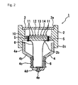
- Fig. 2 is a schematic vertical sectional view of the light emitting device according to Fig. 1 .
- Fig. 3(a) is an enlarged partial vertical sectional view of the SiC fluorescent screen in the light emitting device of Figs. 1 and 2 ; and Fig. 3(b) is a partial plan view of the SiC fluorescent screen.
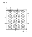
- Fig. 4 is a schematic plan view of the carrier substrate of the first embodiment.
- Figs. 5(a)-5(c) are an explanatory views showing the mounting of LED elements onto the carrier substrate in the first embodiment;
- Fig. 5(a) is a plan view of the carrier substrate before LED elements are mounted;
- Fig. 5(b) is a side view of the carrier substrate at the time of mounting the LED elements;
- Fig. 5(c) is a side view of the carrier substrate after LED elements have been mounted.
- Fig. 6 is a schematic vertical sectional view of another embodiment of the light emitting device.
- Fig. 7 is a schematic depiction of the front of an automobile with headlights incorporating light emitting devices according to the present invention.
- Fig. 8 is a schematic vertical sectional view of another embodiment of a light emitting device for use in the headlights of Fig. 7 .
- Fig. 9 is an explanatory view showing the internal structure of the headlight light emitting device of Fig. 8 .
- Fig. 10(a) is a plan view of a carrier substrate before LED elements are carried;
- Fig. 10(b) is a side view of a carrier substrate at the time of mounting LED elements;
- Fig. 10(c) is a side view of a carrier substrate after LED elements are mounted.
- a light emitting device 1 has a cylindrical body 2 with an opening 2a formed on one end, an SiC fluorescent screen for closing the opening 2a, and an electric terminal part 4 formed on the other end of the body 2.
- a description is given such that the one end of the body 2 is in the upward direction and the other end in the downward direction.
- a SiC fluorescent screen 3 is excited by UV radiation emitted from the LED elements to emit light. Blue light, green light and red light emitted from the LED elements pass through the SiC fluorescent screen 3 without going through any conversion in their wavelengths.
- Fig. 2 is a schematic vertical sectional view of the light emitting device.
- the body 2 shown in Fig. 2 is made of inorganic material. Its lower end is closed off, and the closed part constitutes a bottom part 2b.
- the body 2 is made of ceramics, which is AlN in the present embodiment.
- a carrier substrate 10 on which UV LED elements 11, blue LED elements 12, green LED elements 13 and red LED elements 14 are mounted. Any suitable method may be used for fixing the carrier substrate 10.
- the carrier substrate 10 is fixed with screws that are screwed into the bottom part 2b.
- a step is formed, and the SiC fluorescent screen 3 is fixed on the step part.
- the body 2 has a flange 2c that protrudes downward from the bottom part 2b. In the present embodiment, the flange 2c is formed in the circumferential direction.
- the electric terminal part 4 is made of inorganic material and constituted in a manner for being screwed into a given socket used for supplying electric power.
- the electric terminal part 4 has a cylindrical part 4a that is fixed on the inner circumference of the flange 2c, a sloping part 4b that is formed continuously from the lower end of the cylindrical part 4a and tapers off downward, a first electrode part 4c that is provided on the lower end of the sloping part 4b and has an external surface on which a male screw is formed, an insulating part 4d that is formed continuously from the lower end of the first electrode part 4c and extends inward in the radial direction, and a second electrode 4e that closes off the inner side of the insulating part 4d in the radial direction.
- the cylindrical part 4a, the sloping part 4b and the insulating part 4d are made of ceramics that have insulating properties.
- the first electrode 4c and the second electrode 4e are made of metal that has conductive properties.
- the cylindrical part 4a, the sloping part 4b and the insulating part 4d are preferably made of the same material as that of the body 2.
- the first electrode 4c and the second electrode 4e are electrically connected to a respective one of the screws 5 by internal electric leads 6.
- the screws 5 are made of conductive metal and are electrically connected to a wiring pattern of the carrier substrate 10 when it is screwed into the carrier substrate 10.
- the SiC fluorescent screen 3 is made of 6H type SiC crystals having a periodic structure every six layers and formed in the shape of a plate.
- the SiC fluorescent screen 3 contains N as donor impurities as well as Al and B as acceptor impurities.
- the SiC fluorescent screen 3 is doped with Al having a concentration of 2 x 10 18 cm -3 , for example, B having a concentration of 1 x 10 19 cm -3 , for example, and N having a concentration of 5 x 10 19 cm -3 , for example.
- any concentration is acceptable for Al, B and N, the sum of the concentrations of Al and B must be smaller than the concentration of N in order to excite and emit light from the SiC fluorescent screen 3.
- the SiC fluorescent screen 3 emits fluorescent light as a result of the recombination of donors and acceptors when excited by UV radiation.
- the SiC fluorescent screen 3 can be produced by any suitable method. For example, it can be produced by growing SiC crystals by the sublimation method or the chemical vapor deposition method. In this body, the concentration of nitrogen can be set in any way in the SiC fluorescent screen 3 by properly adjusting the partial pressure of nitrogen gas (N 2 ) in the atmosphere while growing the crystals. On the other hand, the concentrations of Al and B can be set in any way in the SiC fluorescent screen 3 by mixing proper amounts of Al and B singly or proper amounts of an Al compound and a B compound relative to that of raw material.
- the SiC fluorescent screen 3 has a predetermined periodic structure on its front surface and rear surface.
- the periodic structure is constituted of a large number of convex parts 3a substantially having a cone shape.
- Convex parts 3a are periodically arranged along the front surface and the rear surface.
- the shape of each convex part 3a may be a polygonal pyramid, such as a triangular pyramid and a quadrangular pyramid.
- convex parts 3a are arranged in a triangle lattice shape at a predetermined period in a plan view.
- any average period is acceptable for convex parts 3, it is 200 nm in the present embodiment.
- the average period is defined as an average peak distance between convex parts 3a that are adjacent to each other.
- Each convex part 3a substantially has a cone shape: an average bottom diameter is 150 nm and an average height 400 nm.
- the carrier substrate 10 has a square shape in a plan view.
- LED elements 11, 12, 13, 14 are arranged horizontally and vertically at predetermined intervals.
- each LED element 11, 12, 13, 14 is about 350 ⁇ m by 350 ⁇ m square in a plan view.
- the distance between LED elements 11, 12, 13, 14 is about 20 ⁇ m.
- LED elements 11, 12, 13, 14 are not sealed.
- 49 LED elements 11, 12, 13, 14 are mounted on the carrier substrate 10 (7 columns x 7 rows). More specifically, the substrate 10 carries 41 UV LED elements 11, 2 blue LED elements 12, 4 green LED elements 13, and 2 red LED elements 14.
- the UV LED elements 11 emit radiation having a peak wavelength of 380 nm, for example.
- the blue LED elements 12 emit light having a peak wavelength of 450 nm, for example.
- the green LED elements 13 emit light having a peak wavelength of 550 nm, for example.
- the red LED elements 14 emit light having a peak wavelength of 650 nm, for example.
- Material properties are not particularly restricted for the LED elements 11, 12, 13, 14. For example, the following materials may be used: AlInGaN, AlGaN, InGaN, GaN, ZnSe, GaP, GaAsP, AlGaInP, AlGaAs and others.
- the carrier substrate 10 is made of inorganic material that has insulating properties. On its surface a wiring pattern 10a is formed.
- the carrier substrate 10 is made of a ceramic material. In the present embodiment, AlN is used.
- the carrier substrate 10 may also be formed of Si, SiC or the like, for example. Wavelength conversion SiC that is doped with an impurity acceptor and an impurity donor is also acceptable.
- the carrier substrate 10 is tightly attached to the body 2 with a screw 5 at each of its four corners. Of the four screws 5, two diagonally placed screws are electrically connected with the wiring pattern 10a.
- Figs. 5(a)-5(c) are explanatory views showing the mounting of LED elements onto the carrier substrate;
- Figs. 5(a) is a plan view of a carrier substrate before LED elements are mounted;
- Figs. 5(b) is a side view of the carrier substrate at the time of mounting the LED elements;
- Figs. 5(c) is a side view of the carrier substrate after LED elements have been mounted.
- a wiring pattern 10a made of Sn is formed on the carrier substrate 10.
- An Sn film 10b is formed at a position where wiring pattern 10a is electrically connected to each LED element 11.
- flip chip type LED elements 11 are illustrated.
- each LED element is mounted on the Sn film 10b of the carrier substrate 10 with the Au film 11a facing downward.
- the carrier substrate 10 is heated in an atmosphere in which forming gas containing a mixture of hydrogen gas and nitrogen gas is flowing in order to bind each LED chip 11 to the carrier substrate 10.
- each LED chip 11 is connected to the wiring pattern 10a of the carrier substrate 10 through an AuSn alloy 10c.
- each LED element 11, 12, 13, 14 is mounted on the carrier substrate 10 by the following steps:
- the Sn film 10b and the Au film 11 a are contacted with each other in the contacting step by moving the carrying surface of the carrier substrate 10 upward and the mounting surface of each LED element 11, 12, 13, 14 downward, and then, mounting each LED element 11, 12, 13, 14 on the carrier substrate 10.
- each LED element 11, 12, 13, 14 is bound to the carrier substrate 10 by heating the carrier substrate 10 in a state that each LED element 11, 12, 13, 14 is mounted on the carrier substrate 10.
- a wiring pattern 10a made of Sn is formed on the carrier substrate 10 made of inorganic material.
- the Sn film 10b is formed at a position of the carrying surface where each LED element is to be electrically connected.
- This Sn film is formed by an EB deposition method (i.e., electron beam deposition method), for example, and is 1 to 8 ⁇ m in film thickness (e.g., 3 ⁇ m).
- the flip chip type is illustrated for each LED element 11 in Fig. 5(a) .
- an Au film 11a is formed on a pair of electrodes of each LED element 11as the mounting surface.
- This Au film is formed by the EB deposition method, for example, and is 0.1 to 1.0 ⁇ m in film thickness (e.g., 0.2 ⁇ m).
- each LED element 11 is mounted on the Sn film 10b of the carrier substrate 10 by moving the Au film 11a downward.
- the carrier substrate 10 on which LED elements 11, 12, 13, 14 are mounted is placed in a thermal processing container.
- An AuSn type alloy layer 10c alloyed from Sn and Au is formed by heating the carrier substrate 10 in an atmosphere in which forming gas containing a mixture of hydrogen gas and nitrogen gas is flowing.
- the percentage of hydrogen gas contained in this forming gas is less than 10 % (e.g., 5 %).
- the flow rate of the forming gas is 50 to 350 cm 3 /min (e.g., 300 cm 3 /min).
- the thermal processing conditions are as follows: the heating temperature is 250 - 350 °C (e.g., 300 °C) and the processing time 1 - 20 minutes (e.g., 10 minutes). As a result, as shown in Fig.
- each LED chip 11 is bound to the carrier substrate 10 through the AuSn type alloy layer 10c.
- the AuSn type alloy layer 10c is formed by the weight of LED elements 11, 12, 13, 14.
- each LED element 11, 12, 13, 14 may be subject to a pressure of 10 - 50 g/cm 2 , for example.
- the carrier substrate 10 is fixed on the bottom part 2b of the body 2 with screws 5.
- the electric terminal part 4 is connected to the flange 2c of the body 2, and the carrier substrate 10 and the electrode parts 4c, 4e are electrically connected to each other with an internal electric lead 6. In this manner, the light emitting device is made.
- each LED element 11, 12, 13, 14 is bound to the carrier substrate 10 by the weight of each LED element 11, 12, 13, 14, it is not necessarily needed to pressurize each LED element 11, 12, 13, 14, thereby suppressing any harmful influence arising out of pressurization.
- columnar crystals are formed in the AuSn alloy 10c, LED elements 11, 12, 13, 14 can have high emission efficiency for an electric current, whereby excellent heat resistance and heat conductivity are provided to the joining area by AuSn alloy 10c.
- electric power can be supplied to LED elements 11, 12, 13, 14 by screwing the electric terminal part 4 into an external socket.
- an electric current is applied to LED elements 11, 12, 13, 14, radiation having a predetermined wavelength is emitted from those LED elements 11, 12, 13, 14.
- UV radiation emitted from a UV LED element 11 is incident on the SiC fluorescent screen 3 from its rear surface and exits from the front surface of the SiC fluorescent screen 3 after it is absorbed by the SiC fluorescent screen 3 and converted into white light.
- light is emitted by a donor-acceptor pair inside the SiC fluorescent screen 3 using UV radiation as excitation radiation.
- Al and B are doped as acceptors, and pure white color is emitted by light having a broad wavelength spanning from the blue region to the red region with a peak wavelength in the green region. With the emission of this pure white color, it is possible to generate white light having a higher color rendering than that generated by a conventional light emission device that combines a blue LED element and a yellow fluorescent screen.
- Visible light emitted from LED elements 11, 12, 13, 14 other than UV LED elements 11 (blue light, green light and red light in the present embodiment) is incident on the SiC fluorescent screen 3 from its rear surface and then exits form the front surface of the SiC fluorescent screen 3 without going through any conversion in its wavelength. This is because the SiC fluorescent screen 3 is excited by radiation having a wavelength of 408 nm or shorter and is transparent to light that exceeds 408 nm in its wavelength.
- a mixed radiation of white light generated by fluorescent light of the SiC fluorescent screen 3 and blue light green light and red light that pass through the SiC fluorescent screen 3 can be emitted to the outside. Accordingly, a blue component, a green component and a red component can be provided by blue LED elements 12, green LED elements 13 and red LED elements 14 in addition to the pure white fluorescent light of the SiC fluorescent screen 3, thereby generating white light having an extremely high color rendering.
- the luminous flux generated by 41 UV LED 11 was about 280 lm and the luminous flux generated by 2 blue LED elements 12, 4 green LED elements 13 and 2 red LED elements about 20 lm, totaling a luminous flux of about 300 lm.
- the conditions of supplying power to the LED elements 11, 12, 13, 14 were as follows: voltage: 3V; electric current: 20mA; and temperature of the carrier substrate 10: about 70 °C.
- a viewer can perceive that the exited white light is brighter because the number of green LED elements 13 is larger than the number of blue LED elements 12 as well as the number of red LED elements 14. This is because the visual sensitivity of humans is the highest in the green region.
- each LED element 11, 12, 13, 14 emits light
- each LED element 11, 12, 13, 14 generates heat.
- inorganic material is used for the body 2, the SiC fluorescent screen 3, the electric terminal part 4, the carrier substrate 10, and the like in the light emitting device 1 according to the present embodiment
- heat resistance is highly advanced compared with a conventional light emitting device having fluorescent material contained in the sealing resin of an LED element or using a lens made of resin. Accordingly, it is possible to eliminate a heat discharging mechanism that is conventionally needed and to increase the luminous flux by increasing the electric power for the LED elements 11, 12, 13, 14, which is extremely advantageous at the time of practical use. In view of heat resistance, it is preferred to not use any resin in the light emitting device 1.
- each LED element 11, 12, 13, 14 and the carrier substrate 10 are connected to each other by the AuSn type alloy layer 10c in the light emitting device 1 according to the present invention, heat generated in each LED element 11, 12, 13, 14 is smoothly transmitted to the carrier substrate 10.
- the heat transmitted to the carrier substrate 10 is transmitted to the body 2 from the carrier substrate 10 and dissipated to the ambient air.
- the body 2 and the carrier substrate 10 are made of the same material, internal stress caused by differences in thermal expansion coefficients of the parts can be reduced at a time when heat is generated.
- screws 5 made of metal are used for connecting the bottom part 2b of the body 2 with the carrier substrate 10, stress caused by the difference in thermal expansion coefficients is so relatively small that the screws 5 are not damaged because the extending direction of the bottom part 2b and the carrier substrate 10 (horizontal direction) and the extending direction of the screws 5 (vertical direction) are perpendicular to each other.
- a lens 7 made of inorganic material may be provided in the opening 2a of the body 2.
- the lens 7 is made of glass and disposed on the outside of the SiC fluorescent screen 3.
- the exiting surface of the lens 7 has an outwardly (upward) convex shape so that light exiting from the body 2 can be converged. Because the lens 7 is made of inorganic material, this light emitting device 101 has a high heat resistance as well.
- the electric terminal part 4 is screwed into a socket.
- it may be a light emitting device 201 used for a headlight 200a of a motor vehicle 200.
- the vehicle 200 as shown in Fig. 7 is an automobile equipped with headlights 200a on its front part.
- the light emitting device 201 for the headlight 200a as shown in Fig. 8 is not provided with an electric terminal part on the lower portion of the body 2. Instead, a heat sink 8 is connected to the bottom part 2b of the body 2. Also, on the upper portion of the body 2, a reflecting mirror 9 is provided for reflecting light exiting from opening 2a.
- the heat sink 8 can be made small compared with a conventional resin sealing type LED headlight because the heat-resistant temperature is high. No problem occurs if the heat sink is not provided. It is also possible to connect the light emitting device 201 to a certain section of an automobile, thereby using the body of the automobile as a heat discharging member.
- an Au film 11a is formed on each LED element 11 and an Sn film 10b on the carrier substrate 10 to be bound.
- AuSn solder 10d may be formed on the carrier substrate 10 in advance, and then, each LED element 11 is solder-joined on the carrier substrate 10.
- each LED element 11 is of the flip chip type as in the above-mentioned embodiment.
- the LED elements may have a face up joint using a wire 11b as shown in Fig. 10 , for example. Any known method for mounting LED elements can be used for mounting the LED elements 11,12,13,14.
- the above-mentioned embodiment shows an example of 41 UV LED elements 11, 2 blue LED elements 12, 4 green LED elements 13 and 2 red LED elements 14.
- any number of LED elements 11, 12, 13, 14 can be used.
- the percentage of red LED elements 14 can be increased without using blue LED elements 12 in order to generate warm white color.
- the percentage of blue LED elements 12 can be increased without using red LED elements 14.
- any emission wavelength can be used for each LED element so long as LED elements that emit UV radiation are used as the first LED elements and LED elements that emit visible light are used as the second LED element.
- the peak wavelength of the first LED elements is 408 nm or shorter because the SiC fluorescent screen 3 is excited by radiation of 408 nm or shorter wavelengths and that the peak wavelength of the second LED elements exceeds 408 nm.
- LED elements 11, 12, 13, 14 are not sealed. However, they may be sealed by inorganic material, such as transparent glass. In this body, since the sealing material is inorganic, the heat resistance of the light emitting device 1 is not damaged in any way.
- the SiC fluorescent screen 3 is doped with both Al and B as acceptors.
- either one of Al and B may be used as an acceptor for doping.
- fluorescent light having a peak wavelength in the blue region is emitted.
- fluorescent light having a peak wavelength in the yellow region is emitted.
- a reflecting film that reflects UV radiation may be formed on the surface of the SiC fluorescent screen 3 on the exit side.
- This reflecting film may be a multilayered reflecting film (DBR film) made of inorganic material or a film made of inorganic material whose reflective index is higher than that of glass, for example. This method not only prevents UV radiation from exiting to the outside, but also enables reflection of UV radiation to the side of the SiC fluorescent screen 3 in order to convert its wavelength efficiently.
- DBR film multilayered reflecting film
- the body 2, the electric terminal part 4 and the carrier substrate 10 are formed of AlN.
- an inorganic material with other properties can be used (e.g., Si and SiC). It is also possible to use wavelength conversion SiC doped with acceptor impurities and donor impurities. Nevertheless, it is preferred to use the same material in order to make the heat expansion coefficient consistent. It is noted that other specific details of the structure can appropriately be altered as well.
Landscapes
- Engineering & Computer Science (AREA)
- General Engineering & Computer Science (AREA)
- Physics & Mathematics (AREA)
- Microelectronics & Electronic Packaging (AREA)
- Optics & Photonics (AREA)
- Mathematical Physics (AREA)
- Led Device Packages (AREA)
Applications Claiming Priority (2)
| Application Number | Priority Date | Filing Date | Title |
|---|---|---|---|
| JP2008178140A JP2010021202A (ja) | 2008-07-08 | 2008-07-08 | 発光装置 |
| JP2008183557A JP2010027645A (ja) | 2008-07-15 | 2008-07-15 | 発光装置及び発光装置の製造方法 |
Publications (2)
| Publication Number | Publication Date |
|---|---|
| EP2146134A2 true EP2146134A2 (de) | 2010-01-20 |
| EP2146134A3 EP2146134A3 (de) | 2012-09-05 |
Family
ID=41119971
Family Applications (1)
| Application Number | Title | Priority Date | Filing Date |
|---|---|---|---|
| EP09008888A Withdrawn EP2146134A3 (de) | 2008-07-08 | 2009-07-07 | Lichtemittierende Vorrichtung und Verfahren zur Herstellung der lichtemittierenden Vorrichtung |
Country Status (4)
| Country | Link |
|---|---|
| US (1) | US8134166B2 (de) |
| EP (1) | EP2146134A3 (de) |
| KR (1) | KR101266205B1 (de) |
| TW (1) | TW201011197A (de) |
Cited By (5)
| Publication number | Priority date | Publication date | Assignee | Title |
|---|---|---|---|---|
| WO2011101248A1 (de) * | 2010-02-16 | 2011-08-25 | Osram Gesellschaft mit beschränkter Haftung | Leuchtmittel sowie verfahren zu dessen herstellung |
| WO2013029960A1 (en) * | 2011-08-30 | 2013-03-07 | Osram Ag | Led luminaires based on color mixing and remote phosphor arrangement |
| CN105180013A (zh) * | 2015-08-22 | 2015-12-23 | 湖北爱商光电股份有限公司 | Led筒灯 |
| EP2985524A1 (de) * | 2014-08-12 | 2016-02-17 | Zizala Lichtsysteme GmbH | Scheinwerfer für kraftfahrzeuge mit lasereinheit |
| WO2016116576A1 (de) * | 2015-01-21 | 2016-07-28 | Tailorlux Gmbh | Beleuchtungsvorrichtung mit einer leuchtstoffschicht und verschiedenen leuchtdioden |
Families Citing this family (9)
| Publication number | Priority date | Publication date | Assignee | Title |
|---|---|---|---|---|
| CN101858538A (zh) * | 2010-04-26 | 2010-10-13 | 蔡鸿 | 平板led路灯 |
| JP5427705B2 (ja) * | 2010-06-18 | 2014-02-26 | パナソニック株式会社 | 発光ユニット |
| US10107466B2 (en) * | 2010-12-03 | 2018-10-23 | Docter Optics Se | Headlight lens for a vehicle headlight |
| JP2015505172A (ja) * | 2012-01-25 | 2015-02-16 | コーニンクレッカ フィリップス エヌ ヴェ | Ledモジュール、ledユニット、及びledモジュールを備える照明器具 |
| KR20130104628A (ko) * | 2012-03-14 | 2013-09-25 | 서울반도체 주식회사 | Led 조명 모듈 |
| US9293662B2 (en) * | 2012-05-21 | 2016-03-22 | De L Associates Inc. | Light emitting device comprising chip-on-board package substrate and method for manufacturing |
| JP5896297B2 (ja) | 2012-08-01 | 2016-03-30 | 東海カーボン株式会社 | CVD−SiC成形体およびCVD−SiC成形体の製造方法 |
| JP6749240B2 (ja) * | 2014-01-09 | 2020-09-02 | ルミレッズ ホールディング ベーフェー | 反射側壁を有する発光デバイス |
| JP6870592B2 (ja) * | 2017-11-24 | 2021-05-12 | 豊田合成株式会社 | 発光装置 |
Citations (2)
| Publication number | Priority date | Publication date | Assignee | Title |
|---|---|---|---|---|
| US6504179B1 (en) | 2000-05-29 | 2003-01-07 | Patent-Treuhand-Gesellschaft Fur Elektrische Gluhlampen Mbh | Led-based white-emitting illumination unit |
| JP2008085324A (ja) | 2006-09-01 | 2008-04-10 | Intekkusu Kk | 光源装置 |
Family Cites Families (11)
| Publication number | Priority date | Publication date | Assignee | Title |
|---|---|---|---|---|
| JPS5837713B2 (ja) * | 1978-12-01 | 1983-08-18 | 富士通株式会社 | 半導体レ−ザ−装置の製造方法 |
| DE69426090T2 (de) * | 1993-04-27 | 2001-03-01 | Nec Corp., Tokio/Tokyo | Verfahren zur Herstellung einer optische Halbleitervorrichtung |
| US7005679B2 (en) * | 2003-05-01 | 2006-02-28 | Cree, Inc. | Multiple component solid state white light |
| JP2005136006A (ja) * | 2003-10-28 | 2005-05-26 | Matsushita Electric Works Ltd | 発光装置及びそれを用いた演出装置 |
| US7157744B2 (en) * | 2003-10-29 | 2007-01-02 | M/A-Com, Inc. | Surface mount package for a high power light emitting diode |
| US7318651B2 (en) * | 2003-12-18 | 2008-01-15 | Avago Technologies Ecbu Ip (Singapore) Pte. Ltd. | Flash module with quantum dot light conversion |
| JP4496774B2 (ja) * | 2003-12-22 | 2010-07-07 | 日亜化学工業株式会社 | 半導体装置の製造方法 |
| WO2005090515A1 (ja) * | 2004-03-24 | 2005-09-29 | Meijo University | 蛍光体および発光ダイオード |
| US7476910B2 (en) * | 2004-09-10 | 2009-01-13 | Kabushiki Kaisha Toshiba | Semiconductor light emitting device and method for manufacturing the same |
| JP4963867B2 (ja) * | 2006-04-28 | 2012-06-27 | 学校法人 名城大学 | 光制御構造の作成方法、光制御構造および半導体発光素子 |
| JP2010508651A (ja) * | 2006-10-31 | 2010-03-18 | ティーアイアール テクノロジー エルピー | 光励起可能媒体を含む光源 |
-
2009
- 2009-06-12 KR KR1020090052294A patent/KR101266205B1/ko not_active Expired - Fee Related
- 2009-06-16 TW TW098120104A patent/TW201011197A/zh unknown
- 2009-07-07 EP EP09008888A patent/EP2146134A3/de not_active Withdrawn
- 2009-07-07 US US12/498,738 patent/US8134166B2/en not_active Expired - Fee Related
Patent Citations (3)
| Publication number | Priority date | Publication date | Assignee | Title |
|---|---|---|---|---|
| US6504179B1 (en) | 2000-05-29 | 2003-01-07 | Patent-Treuhand-Gesellschaft Fur Elektrische Gluhlampen Mbh | Led-based white-emitting illumination unit |
| JP2003535478A (ja) | 2000-05-29 | 2003-11-25 | パテント−トロイハント−ゲゼルシヤフト フユール エレクトリツシエ グリユーラムペン ミツト ベシユレンクテル ハフツング | Ledをベースとする白色発光照明ユニット |
| JP2008085324A (ja) | 2006-09-01 | 2008-04-10 | Intekkusu Kk | 光源装置 |
Cited By (5)
| Publication number | Priority date | Publication date | Assignee | Title |
|---|---|---|---|---|
| WO2011101248A1 (de) * | 2010-02-16 | 2011-08-25 | Osram Gesellschaft mit beschränkter Haftung | Leuchtmittel sowie verfahren zu dessen herstellung |
| WO2013029960A1 (en) * | 2011-08-30 | 2013-03-07 | Osram Ag | Led luminaires based on color mixing and remote phosphor arrangement |
| EP2985524A1 (de) * | 2014-08-12 | 2016-02-17 | Zizala Lichtsysteme GmbH | Scheinwerfer für kraftfahrzeuge mit lasereinheit |
| WO2016116576A1 (de) * | 2015-01-21 | 2016-07-28 | Tailorlux Gmbh | Beleuchtungsvorrichtung mit einer leuchtstoffschicht und verschiedenen leuchtdioden |
| CN105180013A (zh) * | 2015-08-22 | 2015-12-23 | 湖北爱商光电股份有限公司 | Led筒灯 |
Also Published As
| Publication number | Publication date |
|---|---|
| US8134166B2 (en) | 2012-03-13 |
| KR20100006113A (ko) | 2010-01-18 |
| EP2146134A3 (de) | 2012-09-05 |
| KR101266205B1 (ko) | 2013-05-21 |
| US20100006871A1 (en) | 2010-01-14 |
| TW201011197A (en) | 2010-03-16 |
Similar Documents
| Publication | Publication Date | Title |
|---|---|---|
| US8134166B2 (en) | Light emitting device and method for producing the light emitting device | |
| US8143632B2 (en) | Light emitting device and method for producing the light emitting device | |
| US10297725B2 (en) | Light emitting package having phosphor layer over a transparent resin layer | |
| CN101562225B (zh) | 发光装置 | |
| US8314429B1 (en) | Multi color active regions for white light emitting diode | |
| CN101625084A (zh) | 发光装置及发光装置的制造方法 | |
| US10672959B2 (en) | Light emitting device package and light source apparatus | |
| KR101739573B1 (ko) | 발광소자 | |
| TW201432955A (zh) | 發光元件封裝及其製造方法 | |
| US10672954B2 (en) | Light emitting device package | |
| US10763398B2 (en) | Light emitting device package | |
| US20060118775A1 (en) | Headlamp | |
| JP2010027645A (ja) | 発光装置及び発光装置の製造方法 | |
| JP5301904B2 (ja) | 発光装置 | |
| US12015111B2 (en) | Light emitting device package and light source module | |
| US20160072004A1 (en) | Semiconductor light emitting device | |
| KR20140096652A (ko) | 발광 소자 | |
| WO2024044458A1 (en) | Sealing structures for light-emitting diode packages | |
| US20140231746A1 (en) | Semiconductor light emitting device |
Legal Events
| Date | Code | Title | Description |
|---|---|---|---|
| PUAI | Public reference made under article 153(3) epc to a published international application that has entered the european phase |
Free format text: ORIGINAL CODE: 0009012 |
|
| AK | Designated contracting states |
Kind code of ref document: A2 Designated state(s): AT BE BG CH CY CZ DE DK EE ES FI FR GB GR HR HU IE IS IT LI LT LU LV MC MK MT NL NO PL PT RO SE SI SK SM TR |
|
| AX | Request for extension of the european patent |
Extension state: AL BA RS |
|
| PUAL | Search report despatched |
Free format text: ORIGINAL CODE: 0009013 |
|
| AK | Designated contracting states |
Kind code of ref document: A3 Designated state(s): AT BE BG CH CY CZ DE DK EE ES FI FR GB GR HR HU IE IS IT LI LT LU LV MC MK MT NL NO PL PT RO SE SI SK SM TR |
|
| AX | Request for extension of the european patent |
Extension state: AL BA RS |
|
| RIC1 | Information provided on ipc code assigned before grant |
Ipc: F21V 5/00 20060101ALI20120730BHEP Ipc: F21K 99/00 20100101AFI20120730BHEP Ipc: F21Y 101/02 20060101ALN20120730BHEP |
|
| 17P | Request for examination filed |
Effective date: 20121211 |
|
| 17Q | First examination report despatched |
Effective date: 20130826 |
|
| STAA | Information on the status of an ep patent application or granted ep patent |
Free format text: STATUS: THE APPLICATION IS DEEMED TO BE WITHDRAWN |
|
| 18D | Application deemed to be withdrawn |
Effective date: 20140108 |