EP2141407A1 - Lighting apparatus and lighting unit - Google Patents
Lighting apparatus and lighting unit Download PDFInfo
- Publication number
- EP2141407A1 EP2141407A1 EP08739202A EP08739202A EP2141407A1 EP 2141407 A1 EP2141407 A1 EP 2141407A1 EP 08739202 A EP08739202 A EP 08739202A EP 08739202 A EP08739202 A EP 08739202A EP 2141407 A1 EP2141407 A1 EP 2141407A1
- Authority
- EP
- European Patent Office
- Prior art keywords
- reflection
- light
- lighting apparatus
- reflection surface
- light emitting
- Prior art date
- Legal status (The legal status is an assumption and is not a legal conclusion. Google has not performed a legal analysis and makes no representation as to the accuracy of the status listed.)
- Granted
Links
Images

Classifications
-
- F—MECHANICAL ENGINEERING; LIGHTING; HEATING; WEAPONS; BLASTING
- F21—LIGHTING
- F21V—FUNCTIONAL FEATURES OR DETAILS OF LIGHTING DEVICES OR SYSTEMS THEREOF; STRUCTURAL COMBINATIONS OF LIGHTING DEVICES WITH OTHER ARTICLES, NOT OTHERWISE PROVIDED FOR
- F21V7/00—Reflectors for light sources
- F21V7/04—Optical design
- F21V7/06—Optical design with parabolic curvature
-
- F—MECHANICAL ENGINEERING; LIGHTING; HEATING; WEAPONS; BLASTING
- F21—LIGHTING
- F21K—NON-ELECTRIC LIGHT SOURCES USING LUMINESCENCE; LIGHT SOURCES USING ELECTROCHEMILUMINESCENCE; LIGHT SOURCES USING CHARGES OF COMBUSTIBLE MATERIAL; LIGHT SOURCES USING SEMICONDUCTOR DEVICES AS LIGHT-GENERATING ELEMENTS; LIGHT SOURCES NOT OTHERWISE PROVIDED FOR
- F21K9/00—Light sources using semiconductor devices as light-generating elements, e.g. using light-emitting diodes [LED] or lasers
- F21K9/60—Optical arrangements integrated in the light source, e.g. for improving the colour rendering index or the light extraction
- F21K9/68—Details of reflectors forming part of the light source
-
- F—MECHANICAL ENGINEERING; LIGHTING; HEATING; WEAPONS; BLASTING
- F21—LIGHTING
- F21V—FUNCTIONAL FEATURES OR DETAILS OF LIGHTING DEVICES OR SYSTEMS THEREOF; STRUCTURAL COMBINATIONS OF LIGHTING DEVICES WITH OTHER ARTICLES, NOT OTHERWISE PROVIDED FOR
- F21V7/00—Reflectors for light sources
- F21V7/0083—Array of reflectors for a cluster of light sources, e.g. arrangement of multiple light sources in one plane
-
- F—MECHANICAL ENGINEERING; LIGHTING; HEATING; WEAPONS; BLASTING
- F21—LIGHTING
- F21V—FUNCTIONAL FEATURES OR DETAILS OF LIGHTING DEVICES OR SYSTEMS THEREOF; STRUCTURAL COMBINATIONS OF LIGHTING DEVICES WITH OTHER ARTICLES, NOT OTHERWISE PROVIDED FOR
- F21V7/00—Reflectors for light sources
- F21V7/04—Optical design
- F21V7/09—Optical design with a combination of different curvatures
-
- F—MECHANICAL ENGINEERING; LIGHTING; HEATING; WEAPONS; BLASTING
- F21—LIGHTING
- F21S—NON-PORTABLE LIGHTING DEVICES; SYSTEMS THEREOF; VEHICLE LIGHTING DEVICES SPECIALLY ADAPTED FOR VEHICLE EXTERIORS
- F21S2/00—Systems of lighting devices, not provided for in main groups F21S4/00 - F21S10/00 or F21S19/00, e.g. of modular construction
- F21S2/005—Systems of lighting devices, not provided for in main groups F21S4/00 - F21S10/00 or F21S19/00, e.g. of modular construction of modular construction
-
- F—MECHANICAL ENGINEERING; LIGHTING; HEATING; WEAPONS; BLASTING
- F21—LIGHTING
- F21V—FUNCTIONAL FEATURES OR DETAILS OF LIGHTING DEVICES OR SYSTEMS THEREOF; STRUCTURAL COMBINATIONS OF LIGHTING DEVICES WITH OTHER ARTICLES, NOT OTHERWISE PROVIDED FOR
- F21V7/00—Reflectors for light sources
- F21V7/0091—Reflectors for light sources using total internal reflection
-
- F—MECHANICAL ENGINEERING; LIGHTING; HEATING; WEAPONS; BLASTING
- F21—LIGHTING
- F21Y—INDEXING SCHEME ASSOCIATED WITH SUBCLASSES F21K, F21L, F21S and F21V, RELATING TO THE FORM OR THE KIND OF THE LIGHT SOURCES OR OF THE COLOUR OF THE LIGHT EMITTED
- F21Y2115/00—Light-generating elements of semiconductor light sources
- F21Y2115/10—Light-emitting diodes [LED]
-
- H—ELECTRICITY
- H10—SEMICONDUCTOR DEVICES; ELECTRIC SOLID-STATE DEVICES NOT OTHERWISE PROVIDED FOR
- H10H—INORGANIC LIGHT-EMITTING SEMICONDUCTOR DEVICES HAVING POTENTIAL BARRIERS
- H10H20/00—Individual inorganic light-emitting semiconductor devices having potential barriers, e.g. light-emitting diodes [LED]
- H10H20/80—Constructional details
- H10H20/85—Packages
- H10H20/855—Optical field-shaping means, e.g. lenses
- H10H20/856—Reflecting means
Definitions
- the present invention relates to a lighting apparatus and a lighting unit having light emitting elements, for example, light emitting diodes.
- Lighting apparatuses using light emitting elements such as light emitting diodes have been in development. Lighting apparatuses using such light emitting elements are advantageous in terms of lowering power consumption and prolonging operating life, and thus, are expected to be used widely in place of conventional lighting apparatuses.
- JP-A 2007-59930 is found.
- a conventional lighting apparatus typically has a single light source. Light generated by the single light source is reflected onto a predetermined area by a reflector or the like.
- a plurality of light sources are used, and it is necessary to lead light generated by the plurality of light sources to a predetermined area. Therefore, with respect to the lighting apparatuses using light emitting elements, which are expected to be widely used, it is necessary to solve technical problems that have not been considered regarding the conventional lighting apparatuses.
- a lighting apparatus comprises a plurality of reflection units and a plurality of light sources.
- Each of the plurality of reflection units includes a first reflection surface and a plurality of second reflection surfaces.
- Each of the plurality of second reflection surfaces is arranged around the first reflection surface, and has a shape different from that of the first reflection surface.
- the plurality of light sources are arranged within the first reflection surface and the second reflection surfaces, and each of the plurality of light sources includes a light emitting element made of a semiconductor material.
- a lighting apparatus comprises a plurality of reflection units and a plurality of light sources.
- Each of the plurality of reflection units includes a plurality of reflection surfaces defining a reflection axis, and is capable of varying a direction of the reflection axis.
- the plurality of light sources are arranged within the plurality of reflection surfaces, and each of the plurality of light sources includes a light emitting element made of a semiconductor material.
- a lighting unit comprises a base and a plurality of light emitting elements.
- the lighting unit further comprises a first reflection surface and a second reflection surface.
- the plurality of light emitting elements are made of a semiconductor material and arranged in a plane on the base.
- the first reflection surface surrounds a light emitting element that is located in a central region of the base among the plurality of light emitting elements.
- the second reflection surface has a shape of non-rotational symmetry, and surrounds a light emitting element that is located in a peripheral region of the base among the plurality of light emitting elements.
- the lighting apparatus comprises the second reflection surfaces arranged around the first reflection surface and having a shape different from that of the first reflection surface.
- the lighting apparatus is improved in light emitting property, due to the configuration.
- the lighting apparatus comprises the plurality of reflection units each of which includes the plurality of reflection surfaces defining a reflection axis, and is capable of varying the direction of the reflection axis.
- the lighting apparatus is improved in light emitting property, due to the configuration.
- the lighting unit has a shape of non-rotational symmetry and comprises the second reflection surface surrounding a light emitting element that is located in the peripheral region of the base among the plurality of light emitting elements.
- the lighting unit is improved in light emitting property, due to the configuration.
- a lighting apparatus 100 comprises a plurality of lighting units 100u.
- the plurality of lighting units 100u are arranged two-dimensionally.
- each of the plurality of lighting units 100u comprises a base 11, a reflection unit 12 and a plurality of light sources 13.
- the base 11 is made of an insulating material.
- the reflection unit 12 is provided on the base 11 and is made of a metal material.
- the reflection unit 12 has a plurality of reflection surfaces 12a and 12b.
- the plurality of reflection surfaces 12a and 12b are arranged two-dimensionally. In other words, the plurality of reflection surfaces 12a and 12b are arranged in a plane.
- a reflection axis 12ax is defined by the plurality of reflection surfaces 12a and 12b.
- the reflection axis 12ax means a line connecting a point 12j and an imaginary plane 12p on which the plurality of reflection surfaces 12a and 12b are arranged, at the point 12j light intensity being highest in an imaginary plane 12q that is away from the plane 12p by a predetermined distance (e.g. 50 cm).
- Defining the reflection axis 12ax means that a position and a direction of the reflection axis 12ax are determined by the plurality of reflection surfaces 12a and 12b. More specifically, the position and the direction of the reflection axis 12ax are determined by an arrangement of the plurality of reflection surfaces 12a and 12b and each of their shapes.
- the plurality of reflection surfaces include a first reflection surface 12a and a plurality of second reflection surfaces 12b.
- the first reflection surface 12a has a shape of axial rotational symmetry which results from rotating a curved line around a z-axis in an imaginary xyz-coordinate.
- a shape of axial rotational symmetry means a shape that does not cause any difference, when the shape is rotated around an axis in an imaginary coordinate, between before and after the rotation.
- the first reflection surface 12a has a shape of a portion of paraboloidal surface resulted from a rotation of a parabolic curve around the z-axis in the imaginary xyz-coordinate.
- the first reflection surface 12a has a shape of rotational symmetry in a planar view.
- the planar view means a visual field provided by the line of sight indicated with the reference symbol "v" in Fig. 5 .
- the shape of rotational symmetry means a shape that does not cause any difference, when the shape is rotated around an origin of xy-coordinate in an imaginary xy-coordinate, between before and after the rotation.
- the first reflection surface 12a has a circular shape in a planar view.
- the light source 13 is arranged at the origin of the imaginary xy-coordinate.
- the light source 13 is arranged at a focal point of the first reflection surface 12a, which is a paraboloidal surface. As shown in Fig. 7 , part of light radiated from the light source 13 is reflected by the first reflection surface 12a and propagates as parallel light 12PL.
- Light 12DL which defines a distribution of light 12LD at the first reflection surface 12a is radiated from the light source 13 and exits to an outside of the first reflection surface 12a without being reflected by the first reflection surface 12a.
- the distribution of light 12LD means a range of light that is propagating from the first reflection surface 12a.
- the light which defines the distribution of light means light that defines the range, namely, it means light that is reaching an edge of the range.
- the distribution of light 12LD has a shape of rotational symmetry. The shape of the distribution of light 12LD is circular.
- the first reflection surface 12a is arranged at a central region of the reflection unit 12.
- the first reflection surface 12a is arranged on the reflection axis 12ax. Therefore, in the lighting unit 100u, light intensity is higher at the reflection axis 12ax.
- each of the plurality of second reflection surfaces 12b has a shape different from that of the first reflection surface 12a.
- the second reflection surface 12b has a shape of non-rotational symmetry in a planar view.
- the planar view means a visual field provided by the line of sight indicated with the reference symbol "v" in Fig. 8 .
- the shape of non-rotational symmetry means a shape that causes a mismatch, when the shape is rotated around an origin in an imaginary xy-coordinate, between before and after the rotation.
- the second reflection surface 12b has a first portion 12b-1 located inside and a second portion 12b-2 located outside.
- the second portion 12b-2 has a shape different from that of the first portion 12b-1.
- the first portion 12b-1 reflects the light radiated from the light source 13 in a direction parallel to a propagation direction of the light 12DL defining the distribution of light at the first reflection surface 12a. That is, the first portion 12b-1 reflects the light radiated from the light source 13 upwardly to above the central region of the lighting unit 100u. Therefore, in the lighting unit 100u, light intensity is higher around the reflection axis 12ax.
- the second portion 12b-2 reflects the light radiated from the light source 13 in a direction toward the reflection axis 12ax. Therefore, in the lighting unit 100u, light intensity is higher at the reflection axis 12ax.
- each of the plurality of second reflection surfaces 12b are arranged annularly.
- the second reflection surface 12b has an inside outline 12b-1 and an outside outline 12b-2.
- the inside outline 12b-1 is at a bottom end of the second reflection surface 12b in the imaginary xyz-space.
- the outside outline 12b-2 is at a top end of the second reflection surface 12b in the imaginary xyz-space.
- each of the plurality of second reflection surfaces 12b is arranged around the first reflection surface 12a.
- the inside outline 12b-1 is shifted outwardly within the outside outline 12b-2, relative to an arrangement 12B of the plurality of second reflection surfaces 12b. Therefore, in the lighting unit 100u, light intensity is higher at the reflection axis 12ax.
- the light source 13 comprises a base 13-1, a light emitting element 13-2 and an encapsulation layer 13-3.
- the light source 13 further comprises a light emitting member 13-4.
- the light source 13 is a light emitting diode lamp which emits white light.
- the light source 13 is implemented on the xy-plane in the imaginary xyz-space.
- the white output light D is emitted upwardly.
- the base 13-1 is made of an insulating material.
- An example of the insulating material is ceramics.
- Another example of the insulating material is resin.
- the light emitting element 13-2 is a light emitting diode comprising a plurality of semiconductor layers.
- the light emitting element 13-2 is implemented on the base 13-1.
- the light emitting element 13-2 emits primary light making use of driving electric power.
- the primary light has a wavelength belonging to a blue region or an ultraviolet region.
- the encapsulation layer 13-3 is made of a light transmissive material.
- Light transmissive property of the encapsulation layer 13-3 means that at least part of the primary light radiated from the light emitting element 13-2 passes through the encapsulation layer.
- An example of the material of the encapsulation layer 13-3 is resin.
- the light emitting member 13-4 radiates secondary light in response to the primary light.
- the secondary light has a wavelength different from that of the primary light.
- the wavelength of the secondary light is longer than the wavelength of the primary light.
- the light emitting member 13-4 includes a matrix material and a fluorescence material.
- the matrix material has a light transmissive property.
- the light transmissive property of the matrix material means that at least part of the primary light emitted from the light emitting element 13-2 passes through the matrix material.
- An example of the matrix material is resin. Light radiated from the fluorescence material passes through the matrix material. The fluorescence material is excited by the primary light.
- the plurality of lighting units 100u are movable.
- the plurality of lighting units 100u are capable of varying the direction of the reflection axis 12ax. Therefore, in the lighting apparatus 100, degree of freedom with respect to an area to be illuminated with light and intensity of illuminating light and the like are increased.
Landscapes
- Engineering & Computer Science (AREA)
- General Engineering & Computer Science (AREA)
- Physics & Mathematics (AREA)
- Microelectronics & Electronic Packaging (AREA)
- Optics & Photonics (AREA)
- Non-Portable Lighting Devices Or Systems Thereof (AREA)
Abstract
Description
- The present invention relates to a lighting apparatus and a lighting unit having light emitting elements, for example, light emitting diodes.
- Recently, lighting apparatuses using light emitting elements such as light emitting diodes have been in development. Lighting apparatuses using such light emitting elements are advantageous in terms of lowering power consumption and prolonging operating life, and thus, are expected to be used widely in place of conventional lighting apparatuses. As a related art,
JP-A 2007-59930 - A conventional lighting apparatus typically has a single light source. Light generated by the single light source is reflected onto a predetermined area by a reflector or the like. However, in the lighting apparatus using the light emitting element, currently in development, a plurality of light sources are used, and it is necessary to lead light generated by the plurality of light sources to a predetermined area. Therefore, with respect to the lighting apparatuses using light emitting elements, which are expected to be widely used, it is necessary to solve technical problems that have not been considered regarding the conventional lighting apparatuses.
- In one aspect of the invention, a lighting apparatus comprises a plurality of reflection units and a plurality of light sources. Each of the plurality of reflection units includes a first reflection surface and a plurality of second reflection surfaces. Each of the plurality of second reflection surfaces is arranged around the first reflection surface, and has a shape different from that of the first reflection surface. The plurality of light sources are arranged within the first reflection surface and the second reflection surfaces, and each of the plurality of light sources includes a light emitting element made of a semiconductor material.
- In another aspect of the invention, a lighting apparatus comprises a plurality of reflection units and a plurality of light sources. Each of the plurality of reflection units includes a plurality of reflection surfaces defining a reflection axis, and is capable of varying a direction of the reflection axis. The plurality of light sources are arranged within the plurality of reflection surfaces, and each of the plurality of light sources includes a light emitting element made of a semiconductor material.
- In still another aspect of the invention, a lighting unit comprises a base and a plurality of light emitting elements. The lighting unit further comprises a first reflection surface and a second reflection surface. The plurality of light emitting elements are made of a semiconductor material and arranged in a plane on the base. The first reflection surface surrounds a light emitting element that is located in a central region of the base among the plurality of light emitting elements. The second reflection surface has a shape of non-rotational symmetry, and surrounds a light emitting element that is located in a peripheral region of the base among the plurality of light emitting elements.
- According to the above-mentioned one aspect of the invention, the lighting apparatus comprises the second reflection surfaces arranged around the first reflection surface and having a shape different from that of the first reflection surface. The lighting apparatus is improved in light emitting property, due to the configuration.
- According to the above-mentioned another aspect of the invention, the lighting apparatus comprises the plurality of reflection units each of which includes the plurality of reflection surfaces defining a reflection axis, and is capable of varying the direction of the reflection axis. The lighting apparatus is improved in light emitting property, due to the configuration.
- According to the above-mentioned still another aspect of the invention, the lighting unit has a shape of non-rotational symmetry and comprises the second reflection surface surrounding a light emitting element that is located in the peripheral region of the base among the plurality of light emitting elements. The lighting unit is improved in light emitting property, due to the configuration.
- Other and further objects, features, and advantages of the invention will be more explicit from the following detailed description taken with reference to the drawings wherein:
-
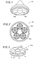
Fig. 1 shows alighting apparatus 100 according to an embodiment of the invention; -
Fig. 2 shows thelighting apparatus 100; -
Fig. 3 shows alighting unit 100u of thelighting apparatus 100; -
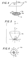
Fig. 4 shows a reflection axis 12ax of areflection unit 12; -
Fig. 5 shows afirst reflection surface 12a of thereflection unit 12; -
Fig. 6 shows a planar view of thefirst reflection surface 12a; -
Fig. 7 shows a distribution of light 12LD at thefirst reflection surface 12a; -
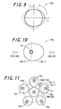
Fig. 8 shows asecond reflection surface 12b of thereflection unit 12; -
Fig. 9 shows a planar view of thesecond reflection surface 12b; -
Fig. 10 shows thesecond reflection surface 12b; -
Fig. 11 shows an arrangement of thefirst reflection surface 12a and thesecond reflection surface 12b; -
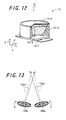
Fig. 12 shows alight source 13; and -
Fig. 13 shows thelighting unit 100u. - Hereafter, an embodiment of the invention will be described with reference to the drawings. As shown in
Figs. 1 and 2 , alighting apparatus 100 comprises a plurality oflighting units 100u. The plurality oflighting units 100u are arranged two-dimensionally. As shown inFig. 3 , each of the plurality oflighting units 100u comprises abase 11, areflection unit 12 and a plurality oflight sources 13. Thebase 11 is made of an insulating material. - The
reflection unit 12 is provided on thebase 11 and is made of a metal material. Thereflection unit 12 has a plurality ofreflection surfaces reflection surfaces reflection surfaces - As shown in
Fig. 4 , a reflection axis 12ax is defined by the plurality ofreflection surfaces point 12j and animaginary plane 12p on which the plurality ofreflection surfaces point 12j light intensity being highest in animaginary plane 12q that is away from theplane 12p by a predetermined distance (e.g. 50 cm). Defining the reflection axis 12ax means that a position and a direction of the reflection axis 12ax are determined by the plurality ofreflection surfaces reflection surfaces - The plurality of reflection surfaces include a
first reflection surface 12a and a plurality ofsecond reflection surfaces 12b. As shown inFig. 5 , thefirst reflection surface 12a has a shape of axial rotational symmetry which results from rotating a curved line around a z-axis in an imaginary xyz-coordinate. A shape of axial rotational symmetry means a shape that does not cause any difference, when the shape is rotated around an axis in an imaginary coordinate, between before and after the rotation. Thefirst reflection surface 12a has a shape of a portion of paraboloidal surface resulted from a rotation of a parabolic curve around the z-axis in the imaginary xyz-coordinate. - As shown in
Fig. 6 , thefirst reflection surface 12a has a shape of rotational symmetry in a planar view. The planar view means a visual field provided by the line of sight indicated with the reference symbol "v" inFig. 5 . The shape of rotational symmetry means a shape that does not cause any difference, when the shape is rotated around an origin of xy-coordinate in an imaginary xy-coordinate, between before and after the rotation. Thefirst reflection surface 12a has a circular shape in a planar view. Thelight source 13 is arranged at the origin of the imaginary xy-coordinate. - The
light source 13 is arranged at a focal point of thefirst reflection surface 12a, which is a paraboloidal surface. As shown inFig. 7 , part of light radiated from thelight source 13 is reflected by thefirst reflection surface 12a and propagates as parallel light 12PL. Light 12DL which defines a distribution of light 12LD at thefirst reflection surface 12a is radiated from thelight source 13 and exits to an outside of thefirst reflection surface 12a without being reflected by thefirst reflection surface 12a. The distribution of light 12LD means a range of light that is propagating from thefirst reflection surface 12a. The light which defines the distribution of light means light that defines the range, namely, it means light that is reaching an edge of the range. The distribution of light 12LD has a shape of rotational symmetry. The shape of the distribution of light 12LD is circular. - The
first reflection surface 12a is arranged at a central region of thereflection unit 12. Thefirst reflection surface 12a is arranged on the reflection axis 12ax. Therefore, in thelighting unit 100u, light intensity is higher at the reflection axis 12ax. - As shown in
Figs. 8 and9 , each of the plurality of second reflection surfaces 12b has a shape different from that of thefirst reflection surface 12a. As shown inFig. 9 , thesecond reflection surface 12b has a shape of non-rotational symmetry in a planar view. The planar view means a visual field provided by the line of sight indicated with the reference symbol "v" inFig. 8 . The shape of non-rotational symmetry means a shape that causes a mismatch, when the shape is rotated around an origin in an imaginary xy-coordinate, between before and after the rotation. - As shown in
Fig. 10 , thesecond reflection surface 12b has afirst portion 12b-1 located inside and asecond portion 12b-2 located outside. Thesecond portion 12b-2 has a shape different from that of thefirst portion 12b-1. - The
first portion 12b-1 reflects the light radiated from thelight source 13 in a direction parallel to a propagation direction of the light 12DL defining the distribution of light at thefirst reflection surface 12a. That is, thefirst portion 12b-1 reflects the light radiated from thelight source 13 upwardly to above the central region of thelighting unit 100u. Therefore, in thelighting unit 100u, light intensity is higher around the reflection axis 12ax. - The
second portion 12b-2 reflects the light radiated from thelight source 13 in a direction toward the reflection axis 12ax. Therefore, in thelighting unit 100u, light intensity is higher at the reflection axis 12ax. - As shown in
Fig. 11 , each of the plurality of second reflection surfaces 12b are arranged annularly. Thesecond reflection surface 12b has aninside outline 12b-1 and anoutside outline 12b-2. As shown inFig. 7 , theinside outline 12b-1 is at a bottom end of thesecond reflection surface 12b in the imaginary xyz-space. Theoutside outline 12b-2 is at a top end of thesecond reflection surface 12b in the imaginary xyz-space. - As shown in
Fig. 11 , each of the plurality of second reflection surfaces 12b is arranged around thefirst reflection surface 12a. Theinside outline 12b-1 is shifted outwardly within theoutside outline 12b-2, relative to anarrangement 12B of the plurality of second reflection surfaces 12b. Therefore, in thelighting unit 100u, light intensity is higher at the reflection axis 12ax. - As shown in
Fig. 12 , thelight source 13 comprises a base 13-1, a light emitting element 13-2 and an encapsulation layer 13-3. Thelight source 13 further comprises a light emitting member 13-4. Thelight source 13 is a light emitting diode lamp which emits white light. InFig. 12 , thelight source 13 is implemented on the xy-plane in the imaginary xyz-space. The white output light D is emitted upwardly. - The base 13-1 is made of an insulating material. An example of the insulating material is ceramics. Another example of the insulating material is resin. The light emitting element 13-2 is a light emitting diode comprising a plurality of semiconductor layers. The light emitting element 13-2 is implemented on the base 13-1. The light emitting element 13-2 emits primary light making use of driving electric power. The primary light has a wavelength belonging to a blue region or an ultraviolet region.
- The encapsulation layer 13-3 is made of a light transmissive material. Light transmissive property of the encapsulation layer 13-3 means that at least part of the primary light radiated from the light emitting element 13-2 passes through the encapsulation layer. An example of the material of the encapsulation layer 13-3 is resin.
- The light emitting member 13-4 radiates secondary light in response to the primary light. The secondary light has a wavelength different from that of the primary light. The wavelength of the secondary light is longer than the wavelength of the primary light.
- The light emitting member 13-4 includes a matrix material and a fluorescence material. The matrix material has a light transmissive property. The light transmissive property of the matrix material means that at least part of the primary light emitted from the light emitting element 13-2 passes through the matrix material. An example of the matrix material is resin. Light radiated from the fluorescence material passes through the matrix material. The fluorescence material is excited by the primary light.
- As shown in
Fig. 13 , the plurality oflighting units 100u are movable. The plurality oflighting units 100u are capable of varying the direction of the reflection axis 12ax. Therefore, in thelighting apparatus 100, degree of freedom with respect to an area to be illuminated with light and intensity of illuminating light and the like are increased. - The invention may be embodied in other specific forms without departing from the spirit or essential characteristics thereof. The present embodiments are therefore to be considered in all respects as illustrative and not restrictive, the scope of the invention being indicated by the appended claims rather than by the foregoing description and all changes which come within the meaning and the range of equivalency of the claims are therefore intended to be embraced therein.
Claims (15)
- A lighting apparatus comprising:a plurality of reflection units each of which includes a first reflection surface and a plurality of second reflection surfaces, each of the plurality of second reflection surfaces being arranged around the first reflection surface and having a shape different from that of the first reflection surface; anda plurality of light sources each of which includes a light emitting element made of a semiconductor material, the plurality of light sources being arranged within the first reflection surface and the second reflection surfaces.
- The lighting apparatus of claim 1, wherein each of the plurality of second reflection surfaces has a shape of non-rotational symmetry.
- The lighting apparatus of claim 2, wherein the first reflection surface has a shape of rotational symmetry.
- The lighting apparatus of claim 3, wherein the first reflection surface has a shape of paraboloid.
- The lighting apparatus of claim 1, wherein each of the plurality of reflection units has a reflection axis defined by the plurality of reflection surfaces.
- The lighting apparatus of claim 5, wherein each of the plurality of reflection units is capable of varying a direction of the reflection axis.
- The lighting apparatus of claim 5, wherein the first reflection surface is arranged on the reflection axis.
- The lighting apparatus of claim 5, wherein the plurality of second reflection surfaces reflect light radiated from the plurality of light sources toward the reflection axis.
- The lighting apparatus of claim 8, wherein each of the plurality of second reflection surfaces reflects the light in a direction parallel to a propagation direction of light defining a distribution of light at the first reflection surface.
- A lighting apparatus comprising:a plurality of reflection units each of which includes a plurality of reflection surfaces defining a reflection axis and is capable of varying a direction of the reflection axis; anda plurality of light sources each of which includes a light emitting element made of a semiconductor material, the plurality of light sources being arranged within the plurality of reflection surfaces.
- The lighting apparatus according to claim 10, wherein, in one reflection unit among the plurality of reflection units, each of the plurality of reflection surfaces is arranged annularly and has an inside outline and an outside outline, and
the inside outline is shifted outwardly within the outside outline, relative to an arrangement of the plurality of reflection surfaces. - The lighting apparatus according to claim 10, wherein, in each of the plurality of reflection units, each of the plurality of reflection surfaces is arranged annularly and has an outside outline,
the plurality of light sources are arranged so as to be shifted outwardly within the outside outline, relative to an arrangement of the plurality of reflection surfaces. - A lighting unit comprising:a base;a plurality of light emitting elements made of a semiconductor material and arranged in a plane on the base;a first reflection surface surrounding a light emitting element that is located in a central region of the base among the plurality of light emitting elements; anda second reflection surface having a shape of non-rotational symmetry, and surrounding a light emitting element that is located in a peripheral region of the base among the plurality of light emitting elements.
- The lighting unit according to claim 13, wherein the first reflection surface has a shape of rotational symmetry.
- The lighting unit according to claim 14, wherein the first reflection surface has a shape of paraboloid.
Applications Claiming Priority (3)
| Application Number | Priority Date | Filing Date | Title |
|---|---|---|---|
| JP2007083937 | 2007-03-28 | ||
| JP2007143960 | 2007-05-30 | ||
| PCT/JP2008/056084 WO2008117865A1 (en) | 2007-03-28 | 2008-03-28 | Lighting apparatus and lighting unit |
Publications (3)
| Publication Number | Publication Date |
|---|---|
| EP2141407A1 true EP2141407A1 (en) | 2010-01-06 |
| EP2141407A4 EP2141407A4 (en) | 2012-05-30 |
| EP2141407B1 EP2141407B1 (en) | 2015-05-13 |
Family
ID=39788596
Family Applications (1)
| Application Number | Title | Priority Date | Filing Date |
|---|---|---|---|
| EP08739202.3A Not-in-force EP2141407B1 (en) | 2007-03-28 | 2008-03-28 | Lighting apparatus and lighting unit |
Country Status (5)
| Country | Link |
|---|---|
| US (1) | US8870411B2 (en) |
| EP (1) | EP2141407B1 (en) |
| JP (1) | JP4982557B2 (en) |
| TW (1) | TWI405351B (en) |
| WO (1) | WO2008117865A1 (en) |
Cited By (2)
| Publication number | Priority date | Publication date | Assignee | Title |
|---|---|---|---|---|
| NL2008163C2 (en) * | 2012-01-20 | 2013-07-25 | Orga Holding B V | Beacon light optic, beacon light, method for obtaining a beacon light optic. |
| EP3300107A1 (en) * | 2016-09-22 | 2018-03-28 | Excellence Opto. Inc. | Light emitting diode array optical cup structure with a focal position |
Families Citing this family (8)
| Publication number | Priority date | Publication date | Assignee | Title |
|---|---|---|---|---|
| KR100928159B1 (en) * | 2008-12-24 | 2009-11-23 | 한성엘컴텍 주식회사 | Light source module and lighting device using the same |
| JP2011171236A (en) * | 2010-02-22 | 2011-09-01 | Panasonic Electric Works Co Ltd | Luminaire |
| JP5534921B2 (en) * | 2010-04-23 | 2014-07-02 | パナソニック株式会社 | lighting equipment |
| JP5624642B2 (en) * | 2013-04-05 | 2014-11-12 | アイリスオーヤマ株式会社 | LED lighting device |
| JP6463026B2 (en) * | 2014-07-29 | 2019-01-30 | 才原 巧 | Light emitting diode lighting device |
| JP6487128B1 (en) * | 2018-01-10 | 2019-03-20 | バルミューダ株式会社 | Lighting equipment |
| KR20190133878A (en) | 2018-05-24 | 2019-12-04 | 엘지이노텍 주식회사 | Lighting module and lighting apparatus |
| CN114153093B (en) * | 2021-12-09 | 2023-04-07 | 武汉华星光电技术有限公司 | Curved surface backlight module and curved surface display device |
Family Cites Families (17)
| Publication number | Priority date | Publication date | Assignee | Title |
|---|---|---|---|---|
| JP3209161B2 (en) * | 1997-10-02 | 2001-09-17 | 松下電器産業株式会社 | Semiconductor light emitting device |
| US6443594B1 (en) | 2000-03-31 | 2002-09-03 | Koninklijke Philips Electronics N.V. | One-piece lens arrays for collimating and focusing light and led light generators using same |
| US6814470B2 (en) * | 2000-05-08 | 2004-11-09 | Farlight Llc | Highly efficient LED lamp |
| US6527411B1 (en) * | 2000-08-01 | 2003-03-04 | Visteon Corporation | Collimating lamp |
| JP2007059930A (en) * | 2001-08-09 | 2007-03-08 | Matsushita Electric Ind Co Ltd | LED lighting device and card type LED illumination light source |
| CN1464953A (en) | 2001-08-09 | 2003-12-31 | 松下电器产业株式会社 | LED lighting device and card type LED lighting source |
| JP4070195B2 (en) * | 2002-11-27 | 2008-04-02 | 京セラ株式会社 | Light emitting element storage package |
| JP2005078937A (en) * | 2003-08-29 | 2005-03-24 | Ichikoh Ind Ltd | Thin light emitting device |
| JP2005285874A (en) * | 2004-03-26 | 2005-10-13 | Kyocera Corp | Light emitting element storage package, light emitting device, and lighting device |
| JP2005340184A (en) * | 2004-04-30 | 2005-12-08 | Du Pont Toray Co Ltd | LED lighting device |
| JP4475109B2 (en) | 2004-11-29 | 2010-06-09 | 岩崎電気株式会社 | Surgical light |
| JP3787148B1 (en) | 2005-09-06 | 2006-06-21 | 株式会社未来 | Lighting unit and lighting device |
| EP1741975B1 (en) * | 2005-07-05 | 2011-09-07 | Frowein EZH GmbH | Operating lamp |
| JP3998027B2 (en) | 2005-07-25 | 2007-10-24 | 松下電工株式会社 | Lighting equipment using LED |
| JP4827575B2 (en) * | 2006-03-29 | 2011-11-30 | 三菱電機株式会社 | lighting equipment |
| US7614766B2 (en) * | 2006-06-29 | 2009-11-10 | Harvatek Corporation | Modular illumination device with adjustable lighting angles |
| JP4018744B1 (en) * | 2006-11-30 | 2007-12-05 | 未来環境開発研究所株式会社 | Lighting device |
-
2008
- 2008-03-28 JP JP2009506382A patent/JP4982557B2/en active Active
- 2008-03-28 EP EP08739202.3A patent/EP2141407B1/en not_active Not-in-force
- 2008-03-28 WO PCT/JP2008/056084 patent/WO2008117865A1/en not_active Ceased
- 2008-03-28 US US12/593,584 patent/US8870411B2/en not_active Expired - Fee Related
- 2008-03-28 TW TW097111530A patent/TWI405351B/en not_active IP Right Cessation
Cited By (4)
| Publication number | Priority date | Publication date | Assignee | Title |
|---|---|---|---|---|
| NL2008163C2 (en) * | 2012-01-20 | 2013-07-25 | Orga Holding B V | Beacon light optic, beacon light, method for obtaining a beacon light optic. |
| WO2013109146A1 (en) * | 2012-01-20 | 2013-07-25 | Orga Holding B.V. | Beacon light optic, beacon light, method for obtaining a beacon light optic |
| US9243763B2 (en) | 2012-01-20 | 2016-01-26 | Orga Holding B.V. | Beacon light optic, beacon light, method for obtaining a beacon light optic |
| EP3300107A1 (en) * | 2016-09-22 | 2018-03-28 | Excellence Opto. Inc. | Light emitting diode array optical cup structure with a focal position |
Also Published As
| Publication number | Publication date |
|---|---|
| EP2141407B1 (en) | 2015-05-13 |
| EP2141407A4 (en) | 2012-05-30 |
| TWI405351B (en) | 2013-08-11 |
| JPWO2008117865A1 (en) | 2010-07-15 |
| JP4982557B2 (en) | 2012-07-25 |
| TW200921944A (en) | 2009-05-16 |
| WO2008117865A1 (en) | 2008-10-02 |
| US20130201684A1 (en) | 2013-08-08 |
| US8870411B2 (en) | 2014-10-28 |
Similar Documents
| Publication | Publication Date | Title |
|---|---|---|
| EP2141407A1 (en) | Lighting apparatus and lighting unit | |
| JP5323998B2 (en) | Luminaire with phosphor, excitation light source, optical system, and heat sink | |
| US8272768B2 (en) | Light emitting device | |
| JP4546579B1 (en) | Lighting lens, light emitting device, surface light source, and liquid crystal display device | |
| JP5336564B2 (en) | Light emitting device, lighting device, vehicle headlamp, and vehicle | |
| US8029167B2 (en) | Light emitting device | |
| AU2016204281B2 (en) | Optical system and lighting device comprised thereof | |
| JP6890287B2 (en) | lighting equipment | |
| JP5555318B2 (en) | Highly efficient light emitting device and method of manufacturing such a device | |
| JP4704296B2 (en) | Vehicle lighting | |
| EP1936261B1 (en) | Illuminating device | |
| CN103765088A (en) | Illumination unit with optical system | |
| JP5840179B2 (en) | Light emitting device | |
| US20150308660A1 (en) | Light engine device | |
| JP5675306B2 (en) | Light emitting device, vehicle headlamp and lighting device | |
| JP6241599B2 (en) | Lighting device | |
| JP2015162447A (en) | Lighting equipment and light source cover | |
| JP6429672B2 (en) | Light emitting device and lighting apparatus using the same | |
| US11846751B1 (en) | Light emitted from decorative cover | |
| JP2013093196A (en) | Led lighting device | |
| CN114576577B (en) | A lighting device and a lamp | |
| JP2011175874A (en) | Lighting fixture and lighting device |
Legal Events
| Date | Code | Title | Description |
|---|---|---|---|
| PUAI | Public reference made under article 153(3) epc to a published international application that has entered the european phase |
Free format text: ORIGINAL CODE: 0009012 |
|
| 17P | Request for examination filed |
Effective date: 20091028 |
|
| AK | Designated contracting states |
Kind code of ref document: A1 Designated state(s): AT BE BG CH CY CZ DE DK EE ES FI FR GB GR HR HU IE IS IT LI LT LU LV MC MT NL NO PL PT RO SE SI SK TR |
|
| DAX | Request for extension of the european patent (deleted) | ||
| A4 | Supplementary search report drawn up and despatched |
Effective date: 20120426 |
|
| RIC1 | Information provided on ipc code assigned before grant |
Ipc: F21S 2/00 20060101ALI20120420BHEP Ipc: F21S 8/04 20060101ALI20120420BHEP Ipc: F21V 14/00 20060101ALI20120420BHEP Ipc: H01L 33/00 20100101ALI20120420BHEP Ipc: F21Y 101/02 20060101ALI20120420BHEP Ipc: F21V 7/00 20060101AFI20120420BHEP Ipc: F21V 7/09 20060101ALI20120420BHEP |
|
| GRAP | Despatch of communication of intention to grant a patent |
Free format text: ORIGINAL CODE: EPIDOSNIGR1 |
|
| INTG | Intention to grant announced |
Effective date: 20141022 |
|
| GRAS | Grant fee paid |
Free format text: ORIGINAL CODE: EPIDOSNIGR3 |
|
| RAP1 | Party data changed (applicant data changed or rights of an application transferred) |
Owner name: KYOCERA CORPORATION |
|
| GRAA | (expected) grant |
Free format text: ORIGINAL CODE: 0009210 |
|
| AK | Designated contracting states |
Kind code of ref document: B1 Designated state(s): AT BE BG CH CY CZ DE DK EE ES FI FR GB GR HR HU IE IS IT LI LT LU LV MC MT NL NO PL PT RO SE SI SK TR |
|
| REG | Reference to a national code |
Ref country code: GB Ref legal event code: FG4D |
|
| REG | Reference to a national code |
Ref country code: CH Ref legal event code: EP |
|
| REG | Reference to a national code |
Ref country code: IE Ref legal event code: FG4D |
|
| REG | Reference to a national code |
Ref country code: AT Ref legal event code: REF Ref document number: 726993 Country of ref document: AT Kind code of ref document: T Effective date: 20150615 |
|
| REG | Reference to a national code |
Ref country code: DE Ref legal event code: R096 Ref document number: 602008038146 Country of ref document: DE Effective date: 20150625 |
|
| REG | Reference to a national code |
Ref country code: AT Ref legal event code: MK05 Ref document number: 726993 Country of ref document: AT Kind code of ref document: T Effective date: 20150513 |
|
| REG | Reference to a national code |
Ref country code: NL Ref legal event code: MP Effective date: 20150513 |
|
| REG | Reference to a national code |
Ref country code: LT Ref legal event code: MG4D |
|
| PG25 | Lapsed in a contracting state [announced via postgrant information from national office to epo] |
Ref country code: PT Free format text: LAPSE BECAUSE OF FAILURE TO SUBMIT A TRANSLATION OF THE DESCRIPTION OR TO PAY THE FEE WITHIN THE PRESCRIBED TIME-LIMIT Effective date: 20150914 Ref country code: LT Free format text: LAPSE BECAUSE OF FAILURE TO SUBMIT A TRANSLATION OF THE DESCRIPTION OR TO PAY THE FEE WITHIN THE PRESCRIBED TIME-LIMIT Effective date: 20150513 Ref country code: NO Free format text: LAPSE BECAUSE OF FAILURE TO SUBMIT A TRANSLATION OF THE DESCRIPTION OR TO PAY THE FEE WITHIN THE PRESCRIBED TIME-LIMIT Effective date: 20150813 Ref country code: ES Free format text: LAPSE BECAUSE OF FAILURE TO SUBMIT A TRANSLATION OF THE DESCRIPTION OR TO PAY THE FEE WITHIN THE PRESCRIBED TIME-LIMIT Effective date: 20150513 Ref country code: HR Free format text: LAPSE BECAUSE OF FAILURE TO SUBMIT A TRANSLATION OF THE DESCRIPTION OR TO PAY THE FEE WITHIN THE PRESCRIBED TIME-LIMIT Effective date: 20150513 Ref country code: FI Free format text: LAPSE BECAUSE OF FAILURE TO SUBMIT A TRANSLATION OF THE DESCRIPTION OR TO PAY THE FEE WITHIN THE PRESCRIBED TIME-LIMIT Effective date: 20150513 |
|
| PG25 | Lapsed in a contracting state [announced via postgrant information from national office to epo] |
Ref country code: AT Free format text: LAPSE BECAUSE OF FAILURE TO SUBMIT A TRANSLATION OF THE DESCRIPTION OR TO PAY THE FEE WITHIN THE PRESCRIBED TIME-LIMIT Effective date: 20150513 Ref country code: IS Free format text: LAPSE BECAUSE OF FAILURE TO SUBMIT A TRANSLATION OF THE DESCRIPTION OR TO PAY THE FEE WITHIN THE PRESCRIBED TIME-LIMIT Effective date: 20150913 Ref country code: GR Free format text: LAPSE BECAUSE OF FAILURE TO SUBMIT A TRANSLATION OF THE DESCRIPTION OR TO PAY THE FEE WITHIN THE PRESCRIBED TIME-LIMIT Effective date: 20150814 Ref country code: LV Free format text: LAPSE BECAUSE OF FAILURE TO SUBMIT A TRANSLATION OF THE DESCRIPTION OR TO PAY THE FEE WITHIN THE PRESCRIBED TIME-LIMIT Effective date: 20150513 Ref country code: BG Free format text: LAPSE BECAUSE OF FAILURE TO SUBMIT A TRANSLATION OF THE DESCRIPTION OR TO PAY THE FEE WITHIN THE PRESCRIBED TIME-LIMIT Effective date: 20150813 |
|
| PG25 | Lapsed in a contracting state [announced via postgrant information from national office to epo] |
Ref country code: DK Free format text: LAPSE BECAUSE OF FAILURE TO SUBMIT A TRANSLATION OF THE DESCRIPTION OR TO PAY THE FEE WITHIN THE PRESCRIBED TIME-LIMIT Effective date: 20150513 Ref country code: EE Free format text: LAPSE BECAUSE OF FAILURE TO SUBMIT A TRANSLATION OF THE DESCRIPTION OR TO PAY THE FEE WITHIN THE PRESCRIBED TIME-LIMIT Effective date: 20150513 |
|
| REG | Reference to a national code |
Ref country code: DE Ref legal event code: R097 Ref document number: 602008038146 Country of ref document: DE |
|
| PG25 | Lapsed in a contracting state [announced via postgrant information from national office to epo] |
Ref country code: RO Free format text: LAPSE BECAUSE OF NON-PAYMENT OF DUE FEES Effective date: 20150513 Ref country code: PL Free format text: LAPSE BECAUSE OF FAILURE TO SUBMIT A TRANSLATION OF THE DESCRIPTION OR TO PAY THE FEE WITHIN THE PRESCRIBED TIME-LIMIT Effective date: 20150513 Ref country code: CZ Free format text: LAPSE BECAUSE OF FAILURE TO SUBMIT A TRANSLATION OF THE DESCRIPTION OR TO PAY THE FEE WITHIN THE PRESCRIBED TIME-LIMIT Effective date: 20150513 Ref country code: SK Free format text: LAPSE BECAUSE OF FAILURE TO SUBMIT A TRANSLATION OF THE DESCRIPTION OR TO PAY THE FEE WITHIN THE PRESCRIBED TIME-LIMIT Effective date: 20150513 |
|
| PLBE | No opposition filed within time limit |
Free format text: ORIGINAL CODE: 0009261 |
|
| STAA | Information on the status of an ep patent application or granted ep patent |
Free format text: STATUS: NO OPPOSITION FILED WITHIN TIME LIMIT |
|
| 26N | No opposition filed |
Effective date: 20160216 |
|
| PG25 | Lapsed in a contracting state [announced via postgrant information from national office to epo] |
Ref country code: IT Free format text: LAPSE BECAUSE OF FAILURE TO SUBMIT A TRANSLATION OF THE DESCRIPTION OR TO PAY THE FEE WITHIN THE PRESCRIBED TIME-LIMIT Effective date: 20150513 |
|
| PG25 | Lapsed in a contracting state [announced via postgrant information from national office to epo] |
Ref country code: SI Free format text: LAPSE BECAUSE OF FAILURE TO SUBMIT A TRANSLATION OF THE DESCRIPTION OR TO PAY THE FEE WITHIN THE PRESCRIBED TIME-LIMIT Effective date: 20150513 |
|
| PG25 | Lapsed in a contracting state [announced via postgrant information from national office to epo] |
Ref country code: BE Free format text: LAPSE BECAUSE OF FAILURE TO SUBMIT A TRANSLATION OF THE DESCRIPTION OR TO PAY THE FEE WITHIN THE PRESCRIBED TIME-LIMIT Effective date: 20150513 |
|
| PG25 | Lapsed in a contracting state [announced via postgrant information from national office to epo] |
Ref country code: LU Free format text: LAPSE BECAUSE OF FAILURE TO SUBMIT A TRANSLATION OF THE DESCRIPTION OR TO PAY THE FEE WITHIN THE PRESCRIBED TIME-LIMIT Effective date: 20160328 Ref country code: MC Free format text: LAPSE BECAUSE OF FAILURE TO SUBMIT A TRANSLATION OF THE DESCRIPTION OR TO PAY THE FEE WITHIN THE PRESCRIBED TIME-LIMIT Effective date: 20150513 |
|
| REG | Reference to a national code |
Ref country code: CH Ref legal event code: PL |
|
| GBPC | Gb: european patent ceased through non-payment of renewal fee |
Effective date: 20160328 |
|
| REG | Reference to a national code |
Ref country code: IE Ref legal event code: MM4A |
|
| REG | Reference to a national code |
Ref country code: FR Ref legal event code: ST Effective date: 20161130 |
|
| PG25 | Lapsed in a contracting state [announced via postgrant information from national office to epo] |
Ref country code: CH Free format text: LAPSE BECAUSE OF NON-PAYMENT OF DUE FEES Effective date: 20160331 Ref country code: FR Free format text: LAPSE BECAUSE OF NON-PAYMENT OF DUE FEES Effective date: 20160331 Ref country code: GB Free format text: LAPSE BECAUSE OF NON-PAYMENT OF DUE FEES Effective date: 20160328 Ref country code: LI Free format text: LAPSE BECAUSE OF NON-PAYMENT OF DUE FEES Effective date: 20160331 Ref country code: IE Free format text: LAPSE BECAUSE OF NON-PAYMENT OF DUE FEES Effective date: 20160328 |
|
| PG25 | Lapsed in a contracting state [announced via postgrant information from national office to epo] |
Ref country code: SE Free format text: LAPSE BECAUSE OF FAILURE TO SUBMIT A TRANSLATION OF THE DESCRIPTION OR TO PAY THE FEE WITHIN THE PRESCRIBED TIME-LIMIT Effective date: 20150513 Ref country code: NL Free format text: LAPSE BECAUSE OF FAILURE TO SUBMIT A TRANSLATION OF THE DESCRIPTION OR TO PAY THE FEE WITHIN THE PRESCRIBED TIME-LIMIT Effective date: 20150513 |
|
| PG25 | Lapsed in a contracting state [announced via postgrant information from national office to epo] |
Ref country code: MT Free format text: LAPSE BECAUSE OF FAILURE TO SUBMIT A TRANSLATION OF THE DESCRIPTION OR TO PAY THE FEE WITHIN THE PRESCRIBED TIME-LIMIT Effective date: 20150513 |
|
| PG25 | Lapsed in a contracting state [announced via postgrant information from national office to epo] |
Ref country code: CY Free format text: LAPSE BECAUSE OF FAILURE TO SUBMIT A TRANSLATION OF THE DESCRIPTION OR TO PAY THE FEE WITHIN THE PRESCRIBED TIME-LIMIT Effective date: 20150513 Ref country code: HU Free format text: LAPSE BECAUSE OF FAILURE TO SUBMIT A TRANSLATION OF THE DESCRIPTION OR TO PAY THE FEE WITHIN THE PRESCRIBED TIME-LIMIT; INVALID AB INITIO Effective date: 20080328 |
|
| PG25 | Lapsed in a contracting state [announced via postgrant information from national office to epo] |
Ref country code: TR Free format text: LAPSE BECAUSE OF FAILURE TO SUBMIT A TRANSLATION OF THE DESCRIPTION OR TO PAY THE FEE WITHIN THE PRESCRIBED TIME-LIMIT Effective date: 20150513 Ref country code: MT Free format text: LAPSE BECAUSE OF FAILURE TO SUBMIT A TRANSLATION OF THE DESCRIPTION OR TO PAY THE FEE WITHIN THE PRESCRIBED TIME-LIMIT Effective date: 20160331 |
|
| RIC2 | Information provided on ipc code assigned after grant |
Ipc: H01L 33/00 20100101ALI20120420BHEP Ipc: F21V 7/09 20060101ALI20120420BHEP Ipc: F21S 8/04 20060101ALI20120420BHEP Ipc: F21V 7/00 20060101AFI20120420BHEP Ipc: F21V 14/00 20180101ALI20120420BHEP Ipc: F21Y 101/02 20000101ALI20120420BHEP Ipc: F21S 2/00 20160101ALI20120420BHEP |
|
| PGFP | Annual fee paid to national office [announced via postgrant information from national office to epo] |
Ref country code: DE Payment date: 20200317 Year of fee payment: 13 |
|
| REG | Reference to a national code |
Ref country code: DE Ref legal event code: R119 Ref document number: 602008038146 Country of ref document: DE |
|
| PG25 | Lapsed in a contracting state [announced via postgrant information from national office to epo] |
Ref country code: DE Free format text: LAPSE BECAUSE OF NON-PAYMENT OF DUE FEES Effective date: 20211001 |