JP5555318B2 - Highly efficient light emitting device and method of manufacturing such a device - Google Patents
Highly efficient light emitting device and method of manufacturing such a device Download PDFInfo
- Publication number
- JP5555318B2 JP5555318B2 JP2012513704A JP2012513704A JP5555318B2 JP 5555318 B2 JP5555318 B2 JP 5555318B2 JP 2012513704 A JP2012513704 A JP 2012513704A JP 2012513704 A JP2012513704 A JP 2012513704A JP 5555318 B2 JP5555318 B2 JP 5555318B2
- Authority
- JP
- Japan
- Prior art keywords
- light
- emitting device
- primary
- optical structure
- light source
- Prior art date
- Legal status (The legal status is an assumption and is not a legal conclusion. Google has not performed a legal analysis and makes no representation as to the accuracy of the status listed.)
- Active
Links
Images


Classifications
-
- F—MECHANICAL ENGINEERING; LIGHTING; HEATING; WEAPONS; BLASTING
- F21—LIGHTING
- F21K—NON-ELECTRIC LIGHT SOURCES USING LUMINESCENCE; LIGHT SOURCES USING ELECTROCHEMILUMINESCENCE; LIGHT SOURCES USING CHARGES OF COMBUSTIBLE MATERIAL; LIGHT SOURCES USING SEMICONDUCTOR DEVICES AS LIGHT-GENERATING ELEMENTS; LIGHT SOURCES NOT OTHERWISE PROVIDED FOR
- F21K9/00—Light sources using semiconductor devices as light-generating elements, e.g. using light-emitting diodes [LED] or lasers
- F21K9/60—Optical arrangements integrated in the light source, e.g. for improving the colour rendering index or the light extraction
- F21K9/64—Optical arrangements integrated in the light source, e.g. for improving the colour rendering index or the light extraction using wavelength conversion means distinct or spaced from the light-generating element, e.g. a remote phosphor layer
-
- F—MECHANICAL ENGINEERING; LIGHTING; HEATING; WEAPONS; BLASTING
- F21—LIGHTING
- F21V—FUNCTIONAL FEATURES OR DETAILS OF LIGHTING DEVICES OR SYSTEMS THEREOF; STRUCTURAL COMBINATIONS OF LIGHTING DEVICES WITH OTHER ARTICLES, NOT OTHERWISE PROVIDED FOR
- F21V5/00—Refractors for light sources
- F21V5/04—Refractors for light sources of lens shape
-
- F—MECHANICAL ENGINEERING; LIGHTING; HEATING; WEAPONS; BLASTING
- F21—LIGHTING
- F21V—FUNCTIONAL FEATURES OR DETAILS OF LIGHTING DEVICES OR SYSTEMS THEREOF; STRUCTURAL COMBINATIONS OF LIGHTING DEVICES WITH OTHER ARTICLES, NOT OTHERWISE PROVIDED FOR
- F21V5/00—Refractors for light sources
- F21V5/10—Refractors for light sources comprising photoluminescent material
-
- H—ELECTRICITY
- H01—ELECTRIC ELEMENTS
- H01L—SEMICONDUCTOR DEVICES NOT COVERED BY CLASS H10
- H01L33/00—Semiconductor devices with at least one potential-jump barrier or surface barrier specially adapted for light emission; Processes or apparatus specially adapted for the manufacture or treatment thereof or of parts thereof; Details thereof
- H01L33/48—Semiconductor devices with at least one potential-jump barrier or surface barrier specially adapted for light emission; Processes or apparatus specially adapted for the manufacture or treatment thereof or of parts thereof; Details thereof characterised by the semiconductor body packages
- H01L33/50—Wavelength conversion elements
- H01L33/507—Wavelength conversion elements the elements being in intimate contact with parts other than the semiconductor body or integrated with parts other than the semiconductor body
-
- H—ELECTRICITY
- H01—ELECTRIC ELEMENTS
- H01L—SEMICONDUCTOR DEVICES NOT COVERED BY CLASS H10
- H01L33/00—Semiconductor devices with at least one potential-jump barrier or surface barrier specially adapted for light emission; Processes or apparatus specially adapted for the manufacture or treatment thereof or of parts thereof; Details thereof
- H01L33/48—Semiconductor devices with at least one potential-jump barrier or surface barrier specially adapted for light emission; Processes or apparatus specially adapted for the manufacture or treatment thereof or of parts thereof; Details thereof characterised by the semiconductor body packages
- H01L33/58—Optical field-shaping elements
-
- F—MECHANICAL ENGINEERING; LIGHTING; HEATING; WEAPONS; BLASTING
- F21—LIGHTING
- F21Y—INDEXING SCHEME ASSOCIATED WITH SUBCLASSES F21K, F21L, F21S and F21V, RELATING TO THE FORM OR THE KIND OF THE LIGHT SOURCES OR OF THE COLOUR OF THE LIGHT EMITTED
- F21Y2115/00—Light-generating elements of semiconductor light sources
- F21Y2115/10—Light-emitting diodes [LED]
-
- H—ELECTRICITY
- H01—ELECTRIC ELEMENTS
- H01L—SEMICONDUCTOR DEVICES NOT COVERED BY CLASS H10
- H01L2924/00—Indexing scheme for arrangements or methods for connecting or disconnecting semiconductor or solid-state bodies as covered by H01L24/00
- H01L2924/0001—Technical content checked by a classifier
- H01L2924/0002—Not covered by any one of groups H01L24/00, H01L24/00 and H01L2224/00
-
- H—ELECTRICITY
- H01—ELECTRIC ELEMENTS
- H01L—SEMICONDUCTOR DEVICES NOT COVERED BY CLASS H10
- H01L33/00—Semiconductor devices with at least one potential-jump barrier or surface barrier specially adapted for light emission; Processes or apparatus specially adapted for the manufacture or treatment thereof or of parts thereof; Details thereof
- H01L33/48—Semiconductor devices with at least one potential-jump barrier or surface barrier specially adapted for light emission; Processes or apparatus specially adapted for the manufacture or treatment thereof or of parts thereof; Details thereof characterised by the semiconductor body packages
- H01L33/50—Wavelength conversion elements
- H01L33/505—Wavelength conversion elements characterised by the shape, e.g. plate or foil
-
- H—ELECTRICITY
- H01—ELECTRIC ELEMENTS
- H01L—SEMICONDUCTOR DEVICES NOT COVERED BY CLASS H10
- H01L33/00—Semiconductor devices with at least one potential-jump barrier or surface barrier specially adapted for light emission; Processes or apparatus specially adapted for the manufacture or treatment thereof or of parts thereof; Details thereof
- H01L33/48—Semiconductor devices with at least one potential-jump barrier or surface barrier specially adapted for light emission; Processes or apparatus specially adapted for the manufacture or treatment thereof or of parts thereof; Details thereof characterised by the semiconductor body packages
- H01L33/58—Optical field-shaping elements
- H01L33/60—Reflective elements
-
- Y—GENERAL TAGGING OF NEW TECHNOLOGICAL DEVELOPMENTS; GENERAL TAGGING OF CROSS-SECTIONAL TECHNOLOGIES SPANNING OVER SEVERAL SECTIONS OF THE IPC; TECHNICAL SUBJECTS COVERED BY FORMER USPC CROSS-REFERENCE ART COLLECTIONS [XRACs] AND DIGESTS
- Y10—TECHNICAL SUBJECTS COVERED BY FORMER USPC
- Y10T—TECHNICAL SUBJECTS COVERED BY FORMER US CLASSIFICATION
- Y10T29/00—Metal working
- Y10T29/49—Method of mechanical manufacture
- Y10T29/49826—Assembling or joining
Landscapes
- Engineering & Computer Science (AREA)
- Microelectronics & Electronic Packaging (AREA)
- General Engineering & Computer Science (AREA)
- Manufacturing & Machinery (AREA)
- Computer Hardware Design (AREA)
- Power Engineering (AREA)
- Physics & Mathematics (AREA)
- Optics & Photonics (AREA)
- Non-Portable Lighting Devices Or Systems Thereof (AREA)
- Led Device Packages (AREA)
- Planar Illumination Modules (AREA)
Description
本発明は効率の高い発光デバイスと、斯様なデバイスを製造する方法とに関する。例えば照明アプリケーション用に斯様なデバイスが使われている。本発明は特に、発光デバイスの効力を高めることに関し、光を変換する媒体を用いて一次光の光源の光が二次光へと変換される。 The present invention relates to highly efficient light-emitting devices and methods for manufacturing such devices. For example, such devices are used for lighting applications. In particular, the present invention relates to increasing the efficacy of a light emitting device, wherein light from a primary light source is converted into secondary light using a light converting medium.
照明アプリケーション及び他のアプリケーション用の、例えば発光ダイオード(LED)を有するソリッドステート光源の使用が急増している。ソリッドステート照明は、非常に効率の高い照明デバイスを提供するという将来性を持っており、斯様な照明デバイスにおいて使われる発光デバイスの効力を更に高めるよう、技術的進歩の狙いが定められる。 There is a surge in the use of solid state light sources, for example with light emitting diodes (LEDs), for lighting applications and other applications. Solid state lighting has the potential to provide very efficient lighting devices, and technological advances are aimed at further enhancing the effectiveness of light emitting devices used in such lighting devices.
しばしば、斯様なアプリケーション用の照明デバイスは白色光を出力することが必要とされる。斯様な照明デバイスを得る方法の一つが、ソリッドステート光源の一次光の少なくとも一部を、蛍光体種を用いて二次光へと変換することである。斯様な蛍光体を有する波長変換物質で青色光を部分的に変換することによって白色光が得られる。例えば発光ダイオード(LED)により発された青色光が、蛍光体によって部分的に吸収され、異なる色の光、例えば黄色光を蛍光体に生じさせる。LEDにより発された青色光が、蛍光体により発された黄色光と混合され、観察者は結果として生じた青色光と黄色光の混合光を白色光として認識する。 Often, lighting devices for such applications are required to output white light. One way to obtain such an illumination device is to convert at least a portion of the primary light of the solid state light source into secondary light using a phosphor species. White light can be obtained by partially converting blue light with a wavelength conversion material having such a phosphor. For example, blue light emitted by a light emitting diode (LED) is partially absorbed by the phosphor, causing light of a different color, such as yellow light, to be produced in the phosphor. The blue light emitted by the LED is mixed with the yellow light emitted by the phosphor, and the observer recognizes the resulting mixed light of blue and yellow light as white light.
しかしながら蛍光体種は、等方性の配光パターンを有する二次光(例えば黄色光)を発する(即ち、二次光が4π以上の立体角で発される)。これ故、二次光の少なくとも一部が一次光の光源の方向へと後方に発されて、吸収される可能性があり、これにより、発光デバイスの効力を減じる。二次光の吸収が50%程度ある。米国特許公開公報US 2009/0001399はLEDのチップと蛍光体とを使用して白色発光ダイオードの照明効力を増す方法を開示している。一次光がLEDチップにより発され、蛍光体によって二次光へと変換される。LEDチップの一次光に対しては透明で、且つ蛍光体の二次光に対しては反射する、少なくとも一つの追加層又は追加材料がLEDチップと蛍光体との間に提供されている。追加層又は追加材料が二次光の吸収を減じる。 However, the phosphor species emit secondary light (for example, yellow light) having an isotropic light distribution pattern (that is, the secondary light is emitted at a solid angle of 4π or more). Thus, at least a portion of the secondary light may be emitted backwards and absorbed in the direction of the primary light source, thereby reducing the effectiveness of the light emitting device. Secondary light absorption is about 50%. US 2009/0001399 discloses a method for increasing the illumination efficiency of white light emitting diodes using LED chips and phosphors. Primary light is emitted by the LED chip and converted to secondary light by the phosphor. At least one additional layer or material is provided between the LED chip and the phosphor that is transparent to the primary light of the LED chip and reflects the secondary light of the phosphor. Additional layers or materials reduce secondary light absorption.
一次光と二次光とに対する追加層又は追加材料の透過率及び反射率は、それぞれ最適ではない。これ故、発光デバイスの効力が依然として更に改善されることができる。 The transmittance and reflectance of the additional layer or material for primary light and secondary light are not optimal respectively. Hence, the efficacy of the light emitting device can still be further improved.
本願明細書では一次光の光源と、光変換媒体と、光学構造部とを有する発光デバイスが開示されている。一次光を発するよう構成された一次光の光源が(例えば一次光の光源用の担体により規定される)第1の面に配置される。一次光の光源の少なくとも一部を一次光の波長とは異なる波長をもつ二次光へと変換するために、光変換媒体が配置される。当該光変換媒体は、一次光の光源から少し離れた場所にある第2の面に配置される。光学構造部は、光変換媒体からの二次光の一部を入力するよう配置され、二次光の出射を可能にするために、二次光の一部を第1の面へと向かう方向で且つ一次光の光源からは離れる方向へとリダイレクトするよう構成される。 In this specification, a light emitting device having a light source of primary light, a light conversion medium, and an optical structure is disclosed. A primary light source configured to emit primary light is disposed on a first surface (eg, defined by a carrier for the primary light source). In order to convert at least part of the light source of the primary light into secondary light having a wavelength different from the wavelength of the primary light, a light conversion medium is arranged. The light conversion medium is disposed on the second surface at a position slightly away from the light source of the primary light. The optical structure is arranged to input a part of the secondary light from the light conversion medium, and in order to allow the secondary light to be emitted, a direction of the part of the secondary light toward the first surface And is configured to redirect away from the light source of the primary light.
エリア又は部屋を照明するための、斯様な発光デバイスを有する照明デバイスも開示されている。 An illumination device having such a light emitting device for illuminating an area or room is also disclosed.
発光デバイスを製造する方法も開示されている。当該製造方法は、一次光を提供するための担体上に一次光の光源を提供するステップと、一次光の光源から少し離れた場所に光変換媒体を配置するステップと、を含む。光変換媒体は一次光の光源の少なくとも一部を、一次光の波長とは異なる波長をもつ二次光へと変換できる。光学構造部が、一次光の光源に面して設けられる。当該光学構造部は光変換媒体からの二次光の一部を入力するよう配置され、二次光の一部を担体に向かう方向で且つ一次光の光源から離れる方向へとリダイレクトするよう配置される。 A method of manufacturing a light emitting device is also disclosed. The manufacturing method includes providing a light source of primary light on a carrier for providing primary light, and disposing a light conversion medium at a position slightly away from the light source of primary light. The light conversion medium can convert at least a part of the light source of the primary light into secondary light having a wavelength different from the wavelength of the primary light. An optical structure is provided facing the primary light source. The optical structure is arranged to input a part of the secondary light from the light conversion medium, and arranged to redirect a part of the secondary light in a direction toward the carrier and away from the light source of the primary light. The
二次光を一次光の光源から離れるようリダイレクトする目的で構成された光学構造部を設けることによって、一次光の光源による二次光の吸収は、中間層又は中間材料を必要とすることなく実質的に減じる又は除去することができる。発光デバイスの一部の構造的な形状変化が、一次光の光源から離れる二次光のリダイレクションを提供する。この二次光を直接的か、又は間接的、即ち更なるリダイレクション構造部を介するか、の何れかで発光デバイスから出射するようにリダイレクトすることによって、発光効率が改善されることができる。 By providing an optical structure configured to redirect the secondary light away from the primary light source, the absorption of the secondary light by the primary light source is substantially eliminated without the need for an intermediate layer or material. Can be reduced or eliminated. The structural shape change of a part of the light emitting device provides secondary light redirection away from the primary light source. By redirecting this secondary light either directly or indirectly, i.e. via a further redirection structure, to be emitted from the light emitting device, the luminous efficiency can be improved.
光学構造部の例は、フレネルレンズ・タイプの構造である。 An example of the optical structure is a Fresnel lens type structure.
第1の面及び第2の面のうちの少なくとも一つは、例えば湾曲する面を有することを理解されたい。平面ではない第2の面の例が、下で更に説明されるであろうドーム形の光変換材料により提供される。 It should be understood that at least one of the first surface and the second surface has a curved surface, for example. An example of a second surface that is not planar is provided by a dome-shaped light converting material that will be further described below.
請求項2、請求項3、及び請求項14の実施例が、二次光の一部のリダイレクションを可能にする効果的な光学構造部を提供するが、一方、一次光に対する透過率及び二次光の一部に対する反射率に関する同構造部の考察とは実質的に独立している。
The embodiments of
請求項4の実施例が製造面からは有益である。更にまた、光学構造部が光変換媒体で形成されていてもよい。 The embodiment of claim 4 is beneficial from a manufacturing standpoint. Furthermore, the optical structure part may be formed of a light conversion medium.
光変換媒体を有するコンポーネントによって一次光が効果的に遮られる点で、請求項5の実施例が好都合である。光変換媒体中の一次光に対する光路が全ての発光角度に対して実質的に同一であり、これにより、等しい二次光の発生を当該コンポーネント上で可能にする点で、請求項6の実施例が有益である。 The embodiment of claim 5 is advantageous in that the primary light is effectively blocked by the component having the light conversion medium. 7. The embodiment of claim 6 in that the optical path for the primary light in the light conversion medium is substantially the same for all emission angles, thereby enabling the generation of equal secondary light on the component. Is beneficial.
請求項7の実施例は、光学構造部を提供するのに比較的容易で且つ経済的で効率的に加工されることができるコンポーネントの材料を提供する。請求項8の実施例は一次光の光源へと向かう光の量を更に減じ、結果として吸収ロスを減じる長所を提供する。 The embodiment of claim 7 provides a component material that is relatively easy to provide an optical structure, and that can be processed economically and efficiently. The embodiment of claim 8 provides the advantage of further reducing the amount of light directed to the primary light source, resulting in reduced absorption losses.
請求項9及び請求項10の実施例は、発光デバイスの効力を増すために、二次光のリダイレクトされた部分を更にリダイレクトする手段を提供する。反射部の反射率は少なくとも95%である。
The embodiments of
国際特許公開公報WO 2008/060586は、遠隔蛍光体発光デバイスの実施例を開示しており、一次光の光源へと向かうインタフェース上で蛍光体層が粗くされていた。粗くされた蛍光体層が一次光の反射を減じることによって、即ち二次光を(リ)ダイレクトするのではなく、蛍光体層の変換効率を改善することを意図している。二次光の有意な量が依然として一次光の光源に行き当たるような二次光に関しては、粗くされた蛍光体層が二次光のランバート配光を一次光と同じく提供することだろう。 International Patent Publication WO 2008/060586 discloses an embodiment of a remote phosphor light emitting device, where the phosphor layer was roughened on the interface towards the primary light source. The roughened phosphor layer is intended to improve the conversion efficiency of the phosphor layer by reducing the reflection of the primary light, i.e. not (re) directing the secondary light. For secondary light where a significant amount of secondary light still strikes the primary light source, the roughened phosphor layer will provide a Lambertian distribution of secondary light as well as the primary light.
図1は、例えばエリア又は空間を照らすための照明アプリケーション用に構成された照明装置1の概観的な例示である。当該照明装置1は発光デバイス2と、ダイクロイックミラー又は反射器などの反射面3とを有する。反射面3を最適に利用するために、発光デバイス2の直径Dは好ましくは小さく、点光源に近い。
FIG. 1 is a schematic illustration of a lighting device 1 configured for a lighting application, for example to illuminate an area or space. The lighting device 1 includes a
図2は、照明装置1の発光デバイス2の平面図を提供している。図3A及び図3Bは、図2の線III〜IIIに沿った断面図である。
FIG. 2 provides a plan view of the
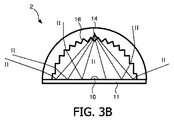
発光デバイス2は、基板11上に提供されている一次光の光源10を有する。一次光の光源10は一つ以上の発光ダイオードを有し、電流がこれらのダイオードを通じて流れることができるように構成されている。この結果、ダイオードは第1の波長をもつ一次光I(例えば360nm乃至480nm、例えば460nmの波長範囲にある青色光)を発する。ダイオードが全て単一の波長の一次光を必ずしも発するわけではないことが理解されるべきである。ハイブリッドな解決案が想定されることができ、幾つかのダイオードが第1の波長(例えば青色)の光を発し、他のダイオードが異なる波長(例えば赤色)の光を発する。(複数の)ダイオードからの一次光の結合を強化するために、例えばシリコン封入材(図示せず)がダイオード上に提供されてもよい。
The
発光デバイス2は、いわゆる遠隔蛍光体をもつ構成を有し、蛍光体物質14を含んでいるコンポーネント13が一次光の光源10から少し離れて配置される。換言すれば、 一次光の光源10は第1の面にあるが、蛍光体物質は第1の面から離れた第2の(湾曲した)面に規定される。一次光の光源10とコンポーネント13との間の典型的な距離は1mm乃至10mmである。蛍光体14は、光変換媒体としての能力で知られている。即ち、第1の波長をもつ発光ダイオードの一次光Iの少なくとも一部を、第1の波長とは異なる第2の波長をもつ二次光IIへと変換する能力で知られている。例えば、青色の一次光が部分的に黄色光へと変換される。青色光及び黄色光の混合物は、観察者に対して白色の輝きWを提供する。異なる変換(即ち、異なる第2の波長)も、例えば蛍光体のタイプの選択に応じて考えられる。例えば、一次光Iを白色の輝きWを提供するために混合する異なる波長をもつ二次光IIへと変換する、複数の異なる蛍光体が選択されてもよい。蛍光体のタイプ及び一次光のタイプに応じてオフ‐ホワイトの照明も得られることが理解されるべきである。
The light-emitting
コンポーネント13はドーム形の外形を有し、一次光の光源10が当該ドームの中心に配置されている。ドーム形のコンポーネント13は、半径方向にかかわりなく等しい光路をコンポーネント13内で一次光Iに提供する。ドーム13は空気チャンバ15を規定しており、これはドーム13の屈折率と当該空気チャンバ15の屈折率との間に少なからぬ差を得るためである。しかしながらチャンバ15が、ドーム13と比較して適切な屈折率の差を有する物質で満たされてもよい。
The
蛍光体14は、全ての方向に均一に二次光IIを発する。これ故、発された二次光IIの一部が不可避的に、外側ではなく一次光の光源10の方向へと後方に導かれる。何らかの対策を採らないと、この二次光IIの相当な部分が一次光の光源10により吸収され、これにより、発光デバイス2の効力を減じる。二次光IIの一部の吸収は、結果として一次光の光源10の相対的な面積がより大きくなるので、より小さな発光源の方が、より多いことであろう。
The
図3A及び図3Bの実施例の目的は、発光デバイス2の後方へと発される二次光の一部が一次光の光源10により吸収されるのを実質的に防止することである。
The purpose of the embodiment of FIGS. 3A and 3B is to substantially prevent a portion of the secondary light emitted behind the
このために、光学構造部16がコンポーネント13と一体化して形成される。光学構造部16は蛍光体14からの二次光IIの一部を入力するよう配置され、図3Bに示すように、二次光の一部を基板11の方へ、しかし一次光の光源10からは離れる方向へとリダイレクトするよう形成される。これ故、一次光の光源10による二次光IIの一部の吸収が実質的に防止されることができる。
For this purpose, the
更に詳細に説明すると、光学構造部16は、蛍光体14によって発生した二次光IIが基板11へ向かう方向へ、しかし一次光の光源10からは離れる方向に屈折するよう配向された、特別に設計された複数の表面17を有する。二次光IIの別の部分は、表面17で内部全反射して、空気チャンバ15に入り込むことなく、コンポーネント13を出てゆくことであろう。
More specifically, the
図3A及び図3Bに例示したように、これらの表面17の方位は、一次光の光源10に対する角度位置に応じてコンポーネント13に沿って変化する。特に、基板11の近くで隣接する面17は互いに直交するよう配向され、一方、一次光の光源10の上では(即ちドーム天頂の近くでは)表面17は、より小さな角度を規定する。
As illustrated in FIGS. 3A and 3B, the orientation of these
発光デバイス2は、基板11に又は同基板上に設けられた反射器18を有する。図2から観察されることができるように、反射器18は光源10を実質的に囲んでいる。二次光IIが最終的に発光デバイス2から出力される確率を増し、これにより、発光デバイス2の発光効率を上昇させるために、光学構造部16によってリダイレクトされた二次光IIの一部が反射器18へと好ましくは導かれる。
The
コンポーネント13は、好ましくはプラスチック(例えばPC若しくはPMMI)又はシリコンにて作られる。これらの材料は比較的安価であり、光学構造部16を提供するために、比較的容易に型成形されることができる。代替的には、コンポーネント13はセラミック材料で作られる。
(複数の)蛍光体14が、コンポーネント13を型成形する前に加えられるか、又は後の工程で加えられる。蛍光体がコンポーネント13の外側に、即ち一次光の光源10から見て外側に、同コンポーネント上に層又はシェルを形成するようコーティングされてもよい。図2、図3A、及び図3Bの実施例のさまざまな変形例が構想されたことを理解されたい。
The phosphor (s) 14 is added before the
図4Aに概観的に例示されている一例は、コンポーネント13に取り付けられた別の層20をもつアプリケーションに関する。当該別の層20は、例えば二次光の一部の屈折によって二次光IIの一部を基板11へと向かう方向へ、しかし一次光の光源10からは離れる方向へとリダイレクトする光学構造部16を有する。
One example schematically illustrated in FIG. 4A relates to an application having another
別の例は、コンポーネント13の異なる構成、即ちドーム形のコンポーネント以外の構成に関する。図4Bは、二次光を基板31へ向かう方向へと導くが、しかし上で説明したように一次光の光源30から距離をおくよう導く表面37を有する光学構造部36を具備している、頭部を切り捨てた逆ピラミッド形のコンポーネント33の概観的な例示を提供している。表面37は隣接する面37が点Aで接するように配向され、一次光の光源30の中心と点Aとの間に描かれた破線が、表面37の鋭角を実質的に等しい角度に分割する。チャンバ35が、頭部を切り捨てた逆ピラミッド形のコンポーネント33の屈折率以下の屈折率を有する空気などの物質で満たされて存在する。
Another example relates to a different configuration of
開示された実施例に対する他のバリエーションが、図面、開示物、及び添付の請求項の学習から、請求された本発明を実施する際に当業者により理解されることができ且つ遂行されることができる。請求項において、単語「有する」が他のエレメント又はステップを除外することはなく、不定冠詞「a」又は「an」が複数を除外することはない。特定の手段が相互に異なる従属請求項において羅列されているという単なる事実は、これらの手段の組合せが有効に使われ得ないとは示していない。請求項中のいかなる参照符号も、本発明の範囲を限定するものとして解釈されてはならない。 Other variations to the disclosed embodiments can be understood and accomplished by those skilled in the art in practicing the claimed invention, from a study of the drawings, disclosure, and appended claims. it can. In the claims, the word “comprising” does not exclude other elements or steps, and the indefinite article “a” or “an” does not exclude a plurality. The mere fact that certain measures are recited in mutually different dependent claims does not indicate that a combination of these measured cannot be used to advantage. Any reference signs in the claims should not be construed as limiting the scope of the invention.
Claims (14)
前記第1の面から距離をおいた第2の面に配置された光変換部であって、少なくとも前記一次光の一部を当該一次光の波長とは異なる波長の二次光へと変換するための光変換部と、
前記第1の面と前記第2の面との間に配置された光学構造部と、を有する、発光デバイスであって、
前記光学構造部は、当該光変換部からの前記二次光の一部が入力され、前記二次光の透過を可能にするために、前記二次光の一部を、前記第1の面へと向かう方向で且つ前記一次光の光源からは離れる方向へと再方向付けする、発光デバイス。 A primary light source disposed on the first surface to emit primary light;
A light converting unit disposed on a second surface spaced from the first surface, wherein at least a part of the primary light is converted into secondary light having a wavelength different from the wavelength of the primary light; A light conversion unit for,
An optical structure disposed between the first surface and the second surface, and a light emitting device,
The optical structure unit receives a part of the secondary light from the light conversion unit, and transmits the secondary light to the first surface to enable transmission of the secondary light. A light-emitting device that redirects in a direction toward and away from the primary light source.
一次光を提供するための一次光の光源を担体上に提供するステップと、
少なくとも前記一次光の一部を当該一次光の波長とは異なる波長をもつ二次光に変換できる光変換部を前記担体から距離をおいて配置するステップと、
光学構造部を前記一次光の光源に面して提供するステップと、
を含み、前記光学構造部は、前記光変換部からの前記二次光の一部が入力され、前記二次光の一部を、前記担体へと向かう方向で且つ前記一次光の光源からは離れる方向へと再方向付けするために配置されていることを特徴とする、方法。 A method of manufacturing a light emitting device, comprising:
Providing a light source of primary light on the carrier to provide primary light;
Disposing at least a distance from the carrier a light conversion unit capable of converting at least part of the primary light into secondary light having a wavelength different from the wavelength of the primary light;
Providing an optical structure facing the light source of the primary light;
The optical structure part receives a part of the secondary light from the light conversion part, and a part of the secondary light is directed from the light source of the primary light in a direction toward the carrier. A method characterized in that it is arranged for redirection in a direction away from it.
Applications Claiming Priority (3)
| Application Number | Priority Date | Filing Date | Title |
|---|---|---|---|
| EP09161945 | 2009-06-04 | ||
| EP09161945.2 | 2009-06-04 | ||
| PCT/IB2010/052365 WO2010143093A1 (en) | 2009-06-04 | 2010-05-27 | Efficient light emitting device and method for manufacturing such a device |
Publications (3)
| Publication Number | Publication Date |
|---|---|
| JP2012529171A JP2012529171A (en) | 2012-11-15 |
| JP2012529171A5 JP2012529171A5 (en) | 2013-07-11 |
| JP5555318B2 true JP5555318B2 (en) | 2014-07-23 |
Family
ID=42563021
Family Applications (1)
| Application Number | Title | Priority Date | Filing Date |
|---|---|---|---|
| JP2012513704A Active JP5555318B2 (en) | 2009-06-04 | 2010-05-27 | Highly efficient light emitting device and method of manufacturing such a device |
Country Status (9)
| Country | Link |
|---|---|
| US (1) | US8690395B2 (en) |
| EP (1) | EP2438630B1 (en) |
| JP (1) | JP5555318B2 (en) |
| KR (2) | KR101749220B1 (en) |
| CN (1) | CN102460747B (en) |
| BR (1) | BRPI1009040A2 (en) |
| RU (1) | RU2525620C2 (en) |
| TW (1) | TWI570964B (en) |
| WO (1) | WO2010143093A1 (en) |
Families Citing this family (8)
| Publication number | Priority date | Publication date | Assignee | Title |
|---|---|---|---|---|
| KR20130128445A (en) | 2010-12-29 | 2013-11-26 | 쓰리엠 이노베이티브 프로퍼티즈 컴파니 | Remote phosphor led constructions |
| RU2452059C1 (en) * | 2011-01-13 | 2012-05-27 | Закрытое Акционерное Общество "Научно-Производственная Коммерческая Фирма "Элтан Лтд" | Light-emitting diode source of white light with remote photoluminescent reflecting converter |
| TW201327926A (en) * | 2011-12-30 | 2013-07-01 | Ind Tech Res Inst | Light conversion structure and the light emitting device packaging structure using the same |
| WO2013182950A1 (en) * | 2012-06-05 | 2013-12-12 | Koninklijke Philips N.V. | Lighting device having a remote wave length converting layer |
| DE102013223947A1 (en) | 2013-11-22 | 2015-05-28 | Osram Gmbh | lighting device |
| KR20170003182A (en) * | 2015-06-30 | 2017-01-09 | 서울반도체 주식회사 | Light emitting diode |
| EP3356875B1 (en) * | 2015-09-29 | 2021-04-14 | Signify Holding B.V. | Led module with output lens |
| JP2018128617A (en) * | 2017-02-10 | 2018-08-16 | 信越化学工業株式会社 | Wavelength conversion member and led light-emitting device |
Family Cites Families (18)
| Publication number | Priority date | Publication date | Assignee | Title |
|---|---|---|---|---|
| JP3268888B2 (en) * | 1992-05-27 | 2002-03-25 | 株式会社デンソー | Light intensity detector |
| RU2219622C1 (en) * | 2002-10-25 | 2003-12-20 | Закрытое акционерное общество "Светлана-Оптоэлектроника" | Semiconductor white light source |
| JP2005003702A (en) * | 2003-06-09 | 2005-01-06 | Konica Minolta Business Technologies Inc | Toner replenishment device |
| US7837348B2 (en) | 2004-05-05 | 2010-11-23 | Rensselaer Polytechnic Institute | Lighting system using multiple colored light emitting sources and diffuser element |
| KR101433343B1 (en) * | 2004-05-05 | 2014-08-22 | 렌슬러 폴리테크닉 인스티튜트 | High efficiency light source using solid-state emitter and down-conversion material |
| US7994527B2 (en) * | 2005-11-04 | 2011-08-09 | The Regents Of The University Of California | High light extraction efficiency light emitting diode (LED) |
| WO2006067885A1 (en) | 2004-12-24 | 2006-06-29 | Kyocera Corporation | Light-emitting device and illuminating device |
| JP2006237264A (en) * | 2005-02-24 | 2006-09-07 | Kyocera Corp | Light emitting device and lighting apparatus |
| JP2006286701A (en) | 2005-03-31 | 2006-10-19 | Mitsubishi Electric Corp | Semiconductor light emitting device |
| KR100665219B1 (en) * | 2005-07-14 | 2007-01-09 | 삼성전기주식회사 | Wavelengt-converted light emitting diode package |
| TWI260801B (en) * | 2005-08-26 | 2006-08-21 | Luminoso Photoelectric Technol | White light emitting device |
| JP2008053702A (en) * | 2006-07-26 | 2008-03-06 | Kyocera Corp | Light-emitting device, and lighting device |
| US7503676B2 (en) * | 2006-07-26 | 2009-03-17 | Kyocera Corporation | Light-emitting device and illuminating apparatus |
| WO2008060586A2 (en) | 2006-11-15 | 2008-05-22 | The Regents Of The University Of California | Textured phosphor conversion layer light emitting diode |
| TWI326924B (en) * | 2007-04-03 | 2010-07-01 | Ching Wu Wang | White light emitting device with phosphor composition and forming method of the phosphor |
| JP2010532104A (en) | 2007-06-27 | 2010-09-30 | ザ リージェンツ オブ ザ ユニバーシティ オブ カリフォルニア | Optical design for high efficiency white light emitting diodes |
| RU82035U1 (en) * | 2008-08-28 | 2009-04-10 | Юрий Андреевич Сазонов | DEVICE FOR MEASURING THICKNESS OF MOVING FILM (OPTIONS) |
| US8168998B2 (en) | 2009-06-09 | 2012-05-01 | Koninklijke Philips Electronics N.V. | LED with remote phosphor layer and reflective submount |
-
2010
- 2010-05-27 JP JP2012513704A patent/JP5555318B2/en active Active
- 2010-05-27 KR KR1020127000266A patent/KR101749220B1/en active IP Right Grant
- 2010-05-27 EP EP10727926.7A patent/EP2438630B1/en active Active
- 2010-05-27 KR KR1020177016188A patent/KR101877695B1/en active IP Right Grant
- 2010-05-27 RU RU2011153969/28A patent/RU2525620C2/en active
- 2010-05-27 BR BRPI1009040A patent/BRPI1009040A2/en not_active Application Discontinuation
- 2010-05-27 WO PCT/IB2010/052365 patent/WO2010143093A1/en active Application Filing
- 2010-05-27 US US13/375,673 patent/US8690395B2/en active Active
- 2010-05-27 CN CN201080024763.XA patent/CN102460747B/en active Active
- 2010-06-01 TW TW099117615A patent/TWI570964B/en active
Also Published As
| Publication number | Publication date |
|---|---|
| RU2011153969A (en) | 2013-07-20 |
| JP2012529171A (en) | 2012-11-15 |
| TWI570964B (en) | 2017-02-11 |
| KR101877695B1 (en) | 2018-07-12 |
| RU2525620C2 (en) | 2014-08-20 |
| US20120087106A1 (en) | 2012-04-12 |
| KR20170085084A (en) | 2017-07-21 |
| WO2010143093A1 (en) | 2010-12-16 |
| KR20120027047A (en) | 2012-03-20 |
| US8690395B2 (en) | 2014-04-08 |
| CN102460747A (en) | 2012-05-16 |
| EP2438630B1 (en) | 2019-05-08 |
| KR101749220B1 (en) | 2017-06-20 |
| CN102460747B (en) | 2015-04-15 |
| TW201104932A (en) | 2011-02-01 |
| BRPI1009040A2 (en) | 2016-08-23 |
| EP2438630A1 (en) | 2012-04-11 |
Similar Documents
| Publication | Publication Date | Title |
|---|---|---|
| US11125926B2 (en) | Planar remote phosphor illumination apparatus | |
| JP5555318B2 (en) | Highly efficient light emitting device and method of manufacturing such a device | |
| US8328406B2 (en) | Low-profile illumination device | |
| JP5047162B2 (en) | Light emitting device | |
| WO2006016324A1 (en) | Light engine | |
| JP2010192439A (en) | Light emitting device and light guide member for the same | |
| JP2011091454A (en) | Light emitting diode element | |
| JP6507035B2 (en) | Light flux control member, light emitting device and lighting device | |
| US8157411B2 (en) | Illuminating device | |
| TWI408307B (en) | Led lamp | |
| US10125950B2 (en) | Optical module | |
| JP2008300298A (en) | Plane lighting light source device and plane lighting device | |
| US20170175955A1 (en) | Led luminaire | |
| JP5057818B2 (en) | Light emitting device | |
| TWI572063B (en) | Light emitting diode package structure | |
| JP6085204B2 (en) | Light emitting device | |
| JP2009158634A (en) | Light-emitting device | |
| JP2009289509A (en) | Illuminating device | |
| WO2023242116A1 (en) | Lighting arrangement with rod-shaped light guide element | |
| KR101878270B1 (en) | Lighting device comprising photoluminescent plate and photoluminescent tape | |
| JP2009158638A (en) | Light-emitting device |
Legal Events
| Date | Code | Title | Description |
|---|---|---|---|
| A521 | Request for written amendment filed |
Free format text: JAPANESE INTERMEDIATE CODE: A523 Effective date: 20130522 |
|
| A621 | Written request for application examination |
Free format text: JAPANESE INTERMEDIATE CODE: A621 Effective date: 20130522 |
|
| A977 | Report on retrieval |
Free format text: JAPANESE INTERMEDIATE CODE: A971007 Effective date: 20140115 |
|
| A131 | Notification of reasons for refusal |
Free format text: JAPANESE INTERMEDIATE CODE: A131 Effective date: 20140116 |
|
| A521 | Request for written amendment filed |
Free format text: JAPANESE INTERMEDIATE CODE: A523 Effective date: 20140416 |
|
| TRDD | Decision of grant or rejection written | ||
| A01 | Written decision to grant a patent or to grant a registration (utility model) |
Free format text: JAPANESE INTERMEDIATE CODE: A01 Effective date: 20140501 |
|
| A61 | First payment of annual fees (during grant procedure) |
Free format text: JAPANESE INTERMEDIATE CODE: A61 Effective date: 20140530 |
|
| R150 | Certificate of patent or registration of utility model |
Ref document number: 5555318 Country of ref document: JP Free format text: JAPANESE INTERMEDIATE CODE: R150 |
|
| R250 | Receipt of annual fees |
Free format text: JAPANESE INTERMEDIATE CODE: R250 |
|
| R250 | Receipt of annual fees |
Free format text: JAPANESE INTERMEDIATE CODE: R250 |
|
| S111 | Request for change of ownership or part of ownership |
Free format text: JAPANESE INTERMEDIATE CODE: R313113 |
|
| R350 | Written notification of registration of transfer |
Free format text: JAPANESE INTERMEDIATE CODE: R350 |
|
| R250 | Receipt of annual fees |
Free format text: JAPANESE INTERMEDIATE CODE: R250 |
|
| R250 | Receipt of annual fees |
Free format text: JAPANESE INTERMEDIATE CODE: R250 |
|
| R250 | Receipt of annual fees |
Free format text: JAPANESE INTERMEDIATE CODE: R250 |
|
| R250 | Receipt of annual fees |
Free format text: JAPANESE INTERMEDIATE CODE: R250 |
|
| R250 | Receipt of annual fees |
Free format text: JAPANESE INTERMEDIATE CODE: R250 |