EP2438630B1 - Efficient light-emitting converted device - Google Patents
Efficient light-emitting converted device Download PDFInfo
- Publication number
- EP2438630B1 EP2438630B1 EP10727926.7A EP10727926A EP2438630B1 EP 2438630 B1 EP2438630 B1 EP 2438630B1 EP 10727926 A EP10727926 A EP 10727926A EP 2438630 B1 EP2438630 B1 EP 2438630B1
- Authority
- EP
- European Patent Office
- Prior art keywords
- light
- emitting device
- light emitting
- primary
- light source
- Prior art date
- Legal status (The legal status is an assumption and is not a legal conclusion. Google has not performed a legal analysis and makes no representation as to the accuracy of the status listed.)
- Active
Links
- 230000003287 optical effect Effects 0.000 claims description 27
- OAICVXFJPJFONN-UHFFFAOYSA-N Phosphorus Chemical compound [P] OAICVXFJPJFONN-UHFFFAOYSA-N 0.000 claims description 24
- 238000005286 illumination Methods 0.000 claims description 14
- 239000000463 material Substances 0.000 claims description 12
- 229920001296 polysiloxane Polymers 0.000 claims description 3
- 230000005540 biological transmission Effects 0.000 claims description 2
- 229910010293 ceramic material Inorganic materials 0.000 claims description 2
- 239000004033 plastic Substances 0.000 claims description 2
- 229920003023 plastic Polymers 0.000 claims description 2
- 230000005855 radiation Effects 0.000 description 9
- 239000000758 substrate Substances 0.000 description 7
- 238000010521 absorption reaction Methods 0.000 description 6
- 238000006243 chemical reaction Methods 0.000 description 4
- 239000007787 solid Substances 0.000 description 4
- 239000000126 substance Substances 0.000 description 4
- 238000004519 manufacturing process Methods 0.000 description 3
- 238000000034 method Methods 0.000 description 3
- 238000002310 reflectometry Methods 0.000 description 3
- CSCPPACGZOOCGX-UHFFFAOYSA-N Acetone Chemical compound CC(C)=O CSCPPACGZOOCGX-UHFFFAOYSA-N 0.000 description 2
- 230000009286 beneficial effect Effects 0.000 description 2
- 230000001419 dependent effect Effects 0.000 description 2
- 239000000203 mixture Substances 0.000 description 2
- 229920003229 poly(methyl methacrylate) Polymers 0.000 description 2
- 239000004926 polymethyl methacrylate Substances 0.000 description 2
- 239000011248 coating agent Substances 0.000 description 1
- 238000000576 coating method Methods 0.000 description 1
- 230000008878 coupling Effects 0.000 description 1
- 238000010168 coupling process Methods 0.000 description 1
- 238000005859 coupling reaction Methods 0.000 description 1
- 238000005516 engineering process Methods 0.000 description 1
- 238000000605 extraction Methods 0.000 description 1
- 239000011521 glass Substances 0.000 description 1
- 238000012986 modification Methods 0.000 description 1
- 230000004048 modification Effects 0.000 description 1
- 238000000465 moulding Methods 0.000 description 1
- 230000000149 penetrating effect Effects 0.000 description 1
- 229920000642 polymer Polymers 0.000 description 1
- 229920013617 polymethylmethyacrylimide Polymers 0.000 description 1
Images


Classifications
-
- F—MECHANICAL ENGINEERING; LIGHTING; HEATING; WEAPONS; BLASTING
- F21—LIGHTING
- F21K—NON-ELECTRIC LIGHT SOURCES USING LUMINESCENCE; LIGHT SOURCES USING ELECTROCHEMILUMINESCENCE; LIGHT SOURCES USING CHARGES OF COMBUSTIBLE MATERIAL; LIGHT SOURCES USING SEMICONDUCTOR DEVICES AS LIGHT-GENERATING ELEMENTS; LIGHT SOURCES NOT OTHERWISE PROVIDED FOR
- F21K9/00—Light sources using semiconductor devices as light-generating elements, e.g. using light-emitting diodes [LED] or lasers
- F21K9/60—Optical arrangements integrated in the light source, e.g. for improving the colour rendering index or the light extraction
- F21K9/64—Optical arrangements integrated in the light source, e.g. for improving the colour rendering index or the light extraction using wavelength conversion means distinct or spaced from the light-generating element, e.g. a remote phosphor layer
-
- F—MECHANICAL ENGINEERING; LIGHTING; HEATING; WEAPONS; BLASTING
- F21—LIGHTING
- F21V—FUNCTIONAL FEATURES OR DETAILS OF LIGHTING DEVICES OR SYSTEMS THEREOF; STRUCTURAL COMBINATIONS OF LIGHTING DEVICES WITH OTHER ARTICLES, NOT OTHERWISE PROVIDED FOR
- F21V5/00—Refractors for light sources
- F21V5/04—Refractors for light sources of lens shape
-
- F—MECHANICAL ENGINEERING; LIGHTING; HEATING; WEAPONS; BLASTING
- F21—LIGHTING
- F21V—FUNCTIONAL FEATURES OR DETAILS OF LIGHTING DEVICES OR SYSTEMS THEREOF; STRUCTURAL COMBINATIONS OF LIGHTING DEVICES WITH OTHER ARTICLES, NOT OTHERWISE PROVIDED FOR
- F21V5/00—Refractors for light sources
- F21V5/10—Refractors for light sources comprising photoluminescent material
-
- H—ELECTRICITY
- H01—ELECTRIC ELEMENTS
- H01L—SEMICONDUCTOR DEVICES NOT COVERED BY CLASS H10
- H01L33/00—Semiconductor devices with at least one potential-jump barrier or surface barrier specially adapted for light emission; Processes or apparatus specially adapted for the manufacture or treatment thereof or of parts thereof; Details thereof
- H01L33/48—Semiconductor devices with at least one potential-jump barrier or surface barrier specially adapted for light emission; Processes or apparatus specially adapted for the manufacture or treatment thereof or of parts thereof; Details thereof characterised by the semiconductor body packages
- H01L33/50—Wavelength conversion elements
- H01L33/507—Wavelength conversion elements the elements being in intimate contact with parts other than the semiconductor body or integrated with parts other than the semiconductor body
-
- H—ELECTRICITY
- H01—ELECTRIC ELEMENTS
- H01L—SEMICONDUCTOR DEVICES NOT COVERED BY CLASS H10
- H01L33/00—Semiconductor devices with at least one potential-jump barrier or surface barrier specially adapted for light emission; Processes or apparatus specially adapted for the manufacture or treatment thereof or of parts thereof; Details thereof
- H01L33/48—Semiconductor devices with at least one potential-jump barrier or surface barrier specially adapted for light emission; Processes or apparatus specially adapted for the manufacture or treatment thereof or of parts thereof; Details thereof characterised by the semiconductor body packages
- H01L33/58—Optical field-shaping elements
-
- F—MECHANICAL ENGINEERING; LIGHTING; HEATING; WEAPONS; BLASTING
- F21—LIGHTING
- F21Y—INDEXING SCHEME ASSOCIATED WITH SUBCLASSES F21K, F21L, F21S and F21V, RELATING TO THE FORM OR THE KIND OF THE LIGHT SOURCES OR OF THE COLOUR OF THE LIGHT EMITTED
- F21Y2115/00—Light-generating elements of semiconductor light sources
- F21Y2115/10—Light-emitting diodes [LED]
-
- H—ELECTRICITY
- H01—ELECTRIC ELEMENTS
- H01L—SEMICONDUCTOR DEVICES NOT COVERED BY CLASS H10
- H01L2924/00—Indexing scheme for arrangements or methods for connecting or disconnecting semiconductor or solid-state bodies as covered by H01L24/00
- H01L2924/0001—Technical content checked by a classifier
- H01L2924/0002—Not covered by any one of groups H01L24/00, H01L24/00 and H01L2224/00
-
- H—ELECTRICITY
- H01—ELECTRIC ELEMENTS
- H01L—SEMICONDUCTOR DEVICES NOT COVERED BY CLASS H10
- H01L33/00—Semiconductor devices with at least one potential-jump barrier or surface barrier specially adapted for light emission; Processes or apparatus specially adapted for the manufacture or treatment thereof or of parts thereof; Details thereof
- H01L33/48—Semiconductor devices with at least one potential-jump barrier or surface barrier specially adapted for light emission; Processes or apparatus specially adapted for the manufacture or treatment thereof or of parts thereof; Details thereof characterised by the semiconductor body packages
- H01L33/50—Wavelength conversion elements
- H01L33/505—Wavelength conversion elements characterised by the shape, e.g. plate or foil
-
- H—ELECTRICITY
- H01—ELECTRIC ELEMENTS
- H01L—SEMICONDUCTOR DEVICES NOT COVERED BY CLASS H10
- H01L33/00—Semiconductor devices with at least one potential-jump barrier or surface barrier specially adapted for light emission; Processes or apparatus specially adapted for the manufacture or treatment thereof or of parts thereof; Details thereof
- H01L33/48—Semiconductor devices with at least one potential-jump barrier or surface barrier specially adapted for light emission; Processes or apparatus specially adapted for the manufacture or treatment thereof or of parts thereof; Details thereof characterised by the semiconductor body packages
- H01L33/58—Optical field-shaping elements
- H01L33/60—Reflective elements
-
- Y—GENERAL TAGGING OF NEW TECHNOLOGICAL DEVELOPMENTS; GENERAL TAGGING OF CROSS-SECTIONAL TECHNOLOGIES SPANNING OVER SEVERAL SECTIONS OF THE IPC; TECHNICAL SUBJECTS COVERED BY FORMER USPC CROSS-REFERENCE ART COLLECTIONS [XRACs] AND DIGESTS
- Y10—TECHNICAL SUBJECTS COVERED BY FORMER USPC
- Y10T—TECHNICAL SUBJECTS COVERED BY FORMER US CLASSIFICATION
- Y10T29/00—Metal working
- Y10T29/49—Method of mechanical manufacture
- Y10T29/49826—Assembling or joining
Definitions
- the invention relates to the field of light emitting devices. Such devices may e.g. be used for illumination applications. More specifically, the invention relates to improving the efficacy of light emitting devices, wherein light of a primary light source is converted to secondary light by using a light converting medium.
- Solid state light sources comprising e.g. light emitting diodes (LEDs)
- LEDs light emitting diodes
- the illumination devices for such applications are required to provide white light.
- One approach to obtain such illumination devices is to convert at least a part of the primary light of the solid state light sources to secondary light using phosphor species.
- White light may be obtained by partial conversion of a blue light with a wavelength converting material comprising such a phosphor.
- the blue light emitted e.g. by a light emitting diode (LED) is partially absorbed by the phosphor, causing the phosphor to emit light of a different color, e.g. a yellow light.
- the blue light emitted by the LED is mixed with the yellow light emitted by the phosphor, and the viewer perceives the resulting mixture of the blue and yellow light as a white light.
- LED light emitting diode
- the phosphor species emit the secondary light (e.g. the yellow light) with an isotropic light distribution pattern (i.e. the secondary light is emitted over a solid angle of 4 ⁇ ). Therefore, at least a part of the secondary light is emitted back in the direction of the primary light source and may be absorbed, thereby reducing the efficacy of the light emitting device.
- the absorption of the secondary light may be as high as 50%.
- US 2009/0001399 A1 discloses a method for increasing the luminous efficacy of a white light emitting diode using a LED die and a phosphor. Primary light is emitted by the LED die and converted to secondary light by the phosphor. At least one additional layer or material is provided between the LED die and the phosphor that is transparent for the primary light from the LED die and reflective for the secondary light of the phosphor. The additional layer or material may reduce the absorption of the secondary light.
- the transparency and the reflectivity of the additional layer or material for the primary light and secondary light, respectively, are not optimal. Therefore, the efficacy of the light emitting device can still be further improved.
- This publication furthermore describes the technical problem which underlies the present invention.
- This problem is the loss caused by phosphor emission light which is directed into the LED chip.
- this problem is lessened by separating the phosphor from the LED and using internal reflection to steer the light away from reflectors and the LED package and out of the device.
- US 2008/0094829 A1 discloses in Figure 7A a light emitting apparatus comprising a radiation source for emitting multi-colored radiation.
- a diffuser material receives at least a portion of the multi-colored radiation emitted by the radiation source and converts the multi-colored radiation into forward transferred radiation and back transferred radiation.
- An optic device is coupled to the diffuser material and is adapted to receive the back transferred radiation and to extract at least a portion of the back transferred radiation from the optic device.
- the present invention aims at improving these prior art light emitting devices so that the losses are even further reduced.
- the light emitting device of the invention is defined in claim 1 and the illumination device of the invention is defined in claim 10. Embodiments of the invention are defined in the dependent claims.
- the light emitting device comprises a primary light source, a light converting medium, an optical structure, and a reflector.
- the primary light source arranged for emitting primary light, is disposed in a first plane (defined by e.g. a carrier for the primary light source) and comprises one or more light emitting diodes.
- the light converting medium is arranged for converting at least a part of the primary light to secondary light of a wavelength different from the wavelength of the primary light.
- the light converting medium is disposed in a second plane at a distance from the primary light source.
- the second plane is curved and/or dome-shaped.
- the optical structure is arranged for receiving a part of the secondary light from the light converting medium and is configured for redirecting the part of the secondary light in a direction towards the first plane and away from the primary light source to enable transmission of the secondary light.
- the optical structure comprising a plurality of surfaces, which surfaces are oriented such that the part of the secondary light being redirected in the direction towards the first plane defines an area at least partially surrounding the primary light source.
- the reflector is provided on or over the first plane for receiving the part of the secondary light redirected by the optical structure.
- absorption of the secondary light by the primary light source can be substantially reduced or eliminated without requiring an intermediate layer or material.
- the structural variation of a part of the light emitting device provides for the redirection of the secondary light away from the primary light source.
- the luminous efficacy is improved by redirecting this secondary light in a direction such that it is transmitted from the light emitting device either directly, or indirectly by the reflector.
- An example of an optical structure would be a Fresnel lens type structure.
- the first plane may comprise e.g. a curved plane.
- the second plane is curved.
- An example of curved second plane is provided by the dome-shaped light conversion material that will be further described below.
- the embodiment of claim 2 provides for an effective optical structure that enables redirection of the part of the secondary light, while being substantially independent of considerations for this structure regarding transparency for primary light and reflectivity for the part of the secondary light.
- the embodiment of claim 3 is beneficial from a manufacturing point.
- the optical structure may be formed in the light converting medium.
- the embodiment of claim 4 is advantageous in that the primary light is effectively intercepted by the component comprising the light converting medium.
- the embodiment of claim 5 is beneficial in that the optical path for the primary light in the light converting medium is substantially identical for all emitting angles thereby allowing equal generation of the secondary light over the component.
- the embodiment of claim 6 provides for materials of the components that can relatively easily and economically efficiently be shaped to provide the optical structure.
- the embodiment of claim 7 provides the advantage of further reducing the amount of light towards the primary light source, therefore reducing absorption losses.
- the reflectivity of the reflector may be at least 95%.
- the illumination device for illuminating an area or a room comprises the light emitting device of the invention.
- a method for manufacturing a light emitting device, method not being part of the invention is also disclosed.
- the manufacturing steps include providing a primary light source on a carrier for providing primary light and disposing a light converting medium at a distance from the primary light source.
- the light converting medium is capable of converting at least a part of the primary light to secondary light of a wavelength different from the wavelength of the primary light.
- An optical structure is provided that faces the primary light source.
- the optical structure is arranged for receiving a part of the secondary light from the light converting medium and for redirecting the part of the secondary light in a direction towards the carrier and away from the primary light source.
- the optical structure comprising a plurality of surfaces, which surfaces are oriented such that the part of the secondary light being redirected in the direction towards the first plane defines an area at least partially surrounding the primary light source.
- WO 2008/060586 A2 discloses an embodiment of a remote phosphor light emitting device wherein the phosphor layer has been roughened on an interface towards the primary light source.
- the roughened phosphor layer is intended to improve the conversion efficiency of the phosphor layer by reducing the reflection of the primary light, i.e. not to (re)-direct the secondary light.
- the roughened phosphor layer would again provide a Lambertian light distribution of secondary light, such that a significant amount of this secondary light would still hit the primary light source.
- FIG. 1 is a schematic illustration of an illumination device 1 configured for an illumination application, e.g. for illuminating an area or space.
- the illumination device 1 comprises a light emitting device 2 and reflective surfaces 3, such as dichroic mirrors or reflectors.
- the diameter D of the light emitting device 2 is preferably small, approximating a point source.
- FIG. 2 provides a top view of the light emitting device 2 of the illumination device 1.
- FIGS. 3A and 3B are cross-sections along line III-III in FIG. 2 .
- the light emitting device 2 comprises a primary light source 10 provided on a substrate 11.
- the primary light source 10 comprises one or more light emitting diodes arranged to allow current to be conveyed through these diodes.
- the diodes emit primary light I of a first wavelength (e.g. blue light in the wavelength range of 360 nm to 480 nm, e.g. 460 nm).
- a first wavelength e.g. blue light in the wavelength range of 360 nm to 480 nm, e.g. 460 nm
- the diodes do not necessarily all emit primary light of a single wavelength.
- Hybrid solutions can be envisaged wherein some diodes emit light of a first wavelength (e.g. blue light) and other diodes emit light of a different wavelength (e.g. red light).
- An encapsulating material may be provided over the diode(s), e.g. silicone, to enhance out coupling of the primary light from the diode(s).
- the light emitting device 2 has a so-called remote phosphor configuration, wherein a component 13 containing phosphor substances 14 is disposed at a distance from the primary light source 10.
- the primary light source 10 is located in a first plane, whereas the phosphor substances are defined in a second, curved plane remote from the first plane.
- a typical distance between the primary light source 10 and the component 13 is between 1 and 10 mm.
- the phosphors 14 are known for their capability as a light converting medium, i.e. to convert at least a part of the primary light I of the light emitting diodes of a first wavelength to secondary light II of a second wavelength being different from the first wavelength.
- blue primary light may be partially converted to yellow light.
- the combination of the blue and yellow light provides for a white luminance W for an observer.
- Different conversions i.e. second wavelengths
- a plurality of different phosphors may be selected that convert the primary light I into secondary light II of different wavelength that mix to provide a white luminance W.
- off-white luminance may also be obtained, depending on the types of phosphors and the primary light.
- the component 13 has a dome shaped configuration, wherein the primary light source 10 is disposed in the centre of the dome.
- a dome-shaped component 13 provides for an equal optical path for primary light I in the component 13, irrespective of the radial direction.
- the dome 13 may define an air chamber 15, such as to obtain a considerable difference between the refraction index of the dome 13 and the air chamber 15.
- the chamber 15 may also be filled with a substance having an appropriate difference in the refraction index as compared to the dome 13.
- the phosphors 14 emit the secondary light II evenly in all directions. Therefore, a part of the emitted secondary light II will unavoidably be directed back into the direction of the primary light source 10 instead of to the outside. Without taking any measures, a considerable part of this secondary light II would be absorbed by the primary light source 10, thereby reducing the efficacy of the light emitting device 2. The absorption of the part of the secondary light II would be greater for smaller light emitting sources as a result of the larger relative area of the primary light source 10.
- FIGS. 3A and 3B The purpose of the embodiment of FIGS. 3A and 3B is to substantially prevent that the part of the secondary light that is emitted back into the light emitting device 2 will be absorbed by the primary light source 10.
- an optical structure 16 is integrally formed in the component 13.
- the optical structure 16 is arranged for receiving a part of the secondary light II from the phosphors 14, as shown in FIG. 3B , and is shaped for redirecting the part of the secondary light in a direction towards the substrate 11 but away from the primary light source 10. Therefore, absorption of the part of the secondary light II by the primary light source 10 can be substantially prevented.
- the optical structure 16 comprises a plurality of specifically designed surfaces 17 that are oriented such that the secondary light II generated by the phosphors 14 is refracted in a direction towards the substrate 11 but away from the primary light source 10. Another part of the secondary light II will experience total internal reflection at the surfaces 17 and may leave the component 13 without penetrating the air chamber 15.
- the orientation of these surfaces 17 varies along the component 13 in dependence of the angular position with respect to the primary light source 10.
- adjacent surfaces 17 are oriented perpendicularly to each other near the substrate 11, whereas the surfaces 17 define a smaller angle above the primary light source 10 (i.e. near the dome zenith).
- the light emitting device 2 comprises a reflector 18 provided on or over the substrate 11.
- the reflector 18 may substantially surround the primary light source 10, as can be observed from FIG. 2 .
- the part of the secondary light II that is redirected by the optical structure 16 is preferably directed to the reflector 18 in order to increase the probability that the secondary light II will eventually be output from the light emitting device 2, thereby increasing the luminous efficacy of the light emitting device 2.
- the component 13 is preferably made of plastic (e.g. PC or PMMI) or silicone. These materials are relatively inexpensive and can relatively easily be molded to provide the optical structure 16. Alternatively, the component 13 is made of a ceramic material.
- Phosphor(s) 14 may be added before molding the component 13 or at a later stage.
- the phosphors may also be coated at the outer side of the component 13, i.e. at the side facing away from the primary light source 10, forming a layer or shell over it.
- the separate layer 20 comprises the optical structure 16 to redirect the part of the secondary light II in a direction towards the substrate 11 but away from the primary light source 10, e.g. by refraction of the part of the secondary light.
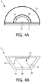
- FIG. 4B provides a schematic illustration of an inversely truncated pyramid component 33 provided with an optical structure 36 comprising surfaces 37 oriented such that secondary light will be directed towards the substrate 31 but away from the primary light source 30 as described above.
- the surfaces 37 are oriented such that adjacent surfaces 37 meet at a point A and a line drawn between the center of the primary light source 30 and the point A divides the sharp angle between the surfaces 37 in substantially equal parts.
- a chamber 35 exists filled with a substance, such as air, having a refractive index below that of the inversely truncated pyramid component 33.
Description
- The invention relates to the field of light emitting devices. Such devices may e.g. be used for illumination applications. More specifically, the invention relates to improving the efficacy of light emitting devices, wherein light of a primary light source is converted to secondary light by using a light converting medium.
- The use of solid state light sources, comprising e.g. light emitting diodes (LEDs), for illumination and other applications increases rapidly. Solid state lighting holds the promise of providing very efficient illumination devices and technological progress is aimed to further improve the efficacy of the light emitting devices used in such illumination devices.
- Often, the illumination devices for such applications are required to provide white light. One approach to obtain such illumination devices is to convert at least a part of the primary light of the solid state light sources to secondary light using phosphor species. White light may be obtained by partial conversion of a blue light with a wavelength converting material comprising such a phosphor. The blue light, emitted e.g. by a light emitting diode (LED) is partially absorbed by the phosphor, causing the phosphor to emit light of a different color, e.g. a yellow light. The blue light emitted by the LED is mixed with the yellow light emitted by the phosphor, and the viewer perceives the resulting mixture of the blue and yellow light as a white light.
- The phosphor species, however, emit the secondary light (e.g. the yellow light) with an isotropic light distribution pattern (i.e. the secondary light is emitted over a solid angle of 4 π). Therefore, at least a part of the secondary light is emitted back in the direction of the primary light source and may be absorbed, thereby reducing the efficacy of the light emitting device. The absorption of the secondary light may be as high as 50%.
US 2009/0001399 A1 discloses a method for increasing the luminous efficacy of a white light emitting diode using a LED die and a phosphor. Primary light is emitted by the LED die and converted to secondary light by the phosphor. At least one additional layer or material is provided between the LED die and the phosphor that is transparent for the primary light from the LED die and reflective for the secondary light of the phosphor. The additional layer or material may reduce the absorption of the secondary light. - The transparency and the reflectivity of the additional layer or material for the primary light and secondary light, respectively, are not optimal. Therefore, the efficacy of the light emitting device can still be further improved.
- The publication by Steven C. Allen et al., entitled "ELiXIR - Solid-State Luminaire With Enhanced Light Extraction by Internal Reflection", in Journal of Display Technology, vol. 3, no. 2, pages 155- 159, published on 1 June 2007, depicts in
Figure 1-b a light emitting device with a primary light source (blue high power LED) and a light converting medium (polymer hemispherical shell lens with an interior phosphor coating). Said shell lens consists of a thin glass inner shell surrounded by a thick polymethyl methacrylate (PMMA) outer shell. Inside said shell, a phosphor containing layer is applied from an acetone solution. The resulting layer has a thickness of appr. 100 µm. - This publication furthermore describes the technical problem which underlies the present invention. This problem is the loss caused by phosphor emission light which is directed into the LED chip. In the prior art device, this problem is lessened by separating the phosphor from the LED and using internal reflection to steer the light away from reflectors and the LED package and out of the device.
-
US 2008/0094829 A1 discloses in Figure 7A a light emitting apparatus comprising a radiation source for emitting multi-colored radiation. A diffuser material receives at least a portion of the multi-colored radiation emitted by the radiation source and converts the multi-colored radiation into forward transferred radiation and back transferred radiation. An optic device is coupled to the diffuser material and is adapted to receive the back transferred radiation and to extract at least a portion of the back transferred radiation from the optic device. - The present invention aims at improving these prior art light emitting devices so that the losses are even further reduced.
- The light emitting device of the invention is defined in
claim 1 and the illumination device of the invention is defined inclaim 10. Embodiments of the invention are defined in the dependent claims. - The light emitting device comprises a primary light source, a light converting medium, an optical structure, and a reflector. The primary light source, arranged for emitting primary light, is disposed in a first plane (defined by e.g. a carrier for the primary light source) and comprises one or more light emitting diodes. The light converting medium is arranged for converting at least a part of the primary light to secondary light of a wavelength different from the wavelength of the primary light. The light converting medium is disposed in a second plane at a distance from the primary light source. The second plane is curved and/or dome-shaped. The optical structure is arranged for receiving a part of the secondary light from the light converting medium and is configured for redirecting the part of the secondary light in a direction towards the first plane and away from the primary light source to enable transmission of the secondary light. For this purpose, the optical structure comprising a plurality of surfaces, which surfaces are oriented such that the part of the secondary light being redirected in the direction towards the first plane defines an area at least partially surrounding the primary light source. The reflector is provided on or over the first plane for receiving the part of the secondary light redirected by the optical structure.
- By providing an optical structure configured for redirecting the secondary light away from the primary light source, absorption of the secondary light by the primary light source can be substantially reduced or eliminated without requiring an intermediate layer or material. The structural variation of a part of the light emitting device provides for the redirection of the secondary light away from the primary light source. The luminous efficacy is improved by redirecting this secondary light in a direction such that it is transmitted from the light emitting device either directly, or indirectly by the reflector.
- An example of an optical structure would be a Fresnel lens type structure.
- It should be appreciated that the first plane may comprise e.g. a curved plane. In accordance with the invention, the second plane is curved. An example of curved second plane is provided by the dome-shaped light conversion material that will be further described below.
- The embodiment of
claim 2 provides for an effective optical structure that enables redirection of the part of the secondary light, while being substantially independent of considerations for this structure regarding transparency for primary light and reflectivity for the part of the secondary light. - The embodiment of
claim 3 is beneficial from a manufacturing point. Furthermore, the optical structure may be formed in the light converting medium. - The embodiment of claim 4 is advantageous in that the primary light is effectively intercepted by the component comprising the light converting medium.
- The embodiment of claim 5 is beneficial in that the optical path for the primary light in the light converting medium is substantially identical for all emitting angles thereby allowing equal generation of the secondary light over the component.
- The embodiment of claim 6 provides for materials of the components that can relatively easily and economically efficiently be shaped to provide the optical structure.
- The embodiment of claim 7 provides the advantage of further reducing the amount of light towards the primary light source, therefore reducing absorption losses.
- The reflectivity of the reflector may be at least 95%.
- The illumination device for illuminating an area or a room comprises the light emitting device of the invention.
- A method for manufacturing a light emitting device, method not being part of the invention, is also disclosed. The manufacturing steps include providing a primary light source on a carrier for providing primary light and disposing a light converting medium at a distance from the primary light source. The light converting medium is capable of converting at least a part of the primary light to secondary light of a wavelength different from the wavelength of the primary light. An optical structure is provided that faces the primary light source. The optical structure is arranged for receiving a part of the secondary light from the light converting medium and for redirecting the part of the secondary light in a direction towards the carrier and away from the primary light source. For this purpose, the optical structure comprising a plurality of surfaces, which surfaces are oriented such that the part of the secondary light being redirected in the direction towards the first plane defines an area at least partially surrounding the primary light source.
-
WO 2008/060586 A2 discloses an embodiment of a remote phosphor light emitting device wherein the phosphor layer has been roughened on an interface towards the primary light source. The roughened phosphor layer is intended to improve the conversion efficiency of the phosphor layer by reducing the reflection of the primary light, i.e. not to (re)-direct the secondary light. For secondary light, the roughened phosphor layer would again provide a Lambertian light distribution of secondary light, such that a significant amount of this secondary light would still hit the primary light source. -
-
FIG. 1 provides a schematic illustration of an illumination device comprising a light emitting device according to an embodiment of the invention; -
FIG. 2 provides a schematic illustration of a top view of a light emitting device according to an embodiment of the invention; -
FIGS. 3A and 3B provide schematic illustrations of a cross-section of the light emitting device ofFIG. 2 along III-III; and -
FIGS. 4A and 4B provide alternative light emitting devices; he device ofFIG. 4A is according to an embodiment of the invention, whereas the device ofFIG. 4B is not forming part of the invention. -
FIG. 1 is a schematic illustration of anillumination device 1 configured for an illumination application, e.g. for illuminating an area or space. Theillumination device 1 comprises alight emitting device 2 andreflective surfaces 3, such as dichroic mirrors or reflectors. In order to make optimal use of thereflective surfaces 3, the diameter D of thelight emitting device 2 is preferably small, approximating a point source. -
FIG. 2 provides a top view of thelight emitting device 2 of theillumination device 1.FIGS. 3A and 3B are cross-sections along line III-III inFIG. 2 . - The
light emitting device 2 comprises a primarylight source 10 provided on asubstrate 11. Theprimary light source 10 comprises one or more light emitting diodes arranged to allow current to be conveyed through these diodes. As a result, the diodes emit primary light I of a first wavelength (e.g. blue light in the wavelength range of 360 nm to 480 nm, e.g. 460 nm). It should be appreciated that the diodes do not necessarily all emit primary light of a single wavelength. Hybrid solutions can be envisaged wherein some diodes emit light of a first wavelength (e.g. blue light) and other diodes emit light of a different wavelength (e.g. red light). An encapsulating material (not shown) may be provided over the diode(s), e.g. silicone, to enhance out coupling of the primary light from the diode(s). - The
light emitting device 2 has a so-called remote phosphor configuration, wherein acomponent 13 containingphosphor substances 14 is disposed at a distance from theprimary light source 10. In other words, theprimary light source 10 is located in a first plane, whereas the phosphor substances are defined in a second, curved plane remote from the first plane. A typical distance between theprimary light source 10 and thecomponent 13 is between 1 and 10 mm. Thephosphors 14 are known for their capability as a light converting medium, i.e. to convert at least a part of the primary light I of the light emitting diodes of a first wavelength to secondary light II of a second wavelength being different from the first wavelength. As an example, blue primary light may be partially converted to yellow light. The combination of the blue and yellow light provides for a white luminance W for an observer. Different conversions (i.e. second wavelengths) are possible, depending e.g. on the selected type(s) of phosphors. As an example, a plurality of different phosphors may be selected that convert the primary light I into secondary light II of different wavelength that mix to provide a white luminance W. It should be appreciated that off-white luminance may also be obtained, depending on the types of phosphors and the primary light. - The
component 13 has a dome shaped configuration, wherein theprimary light source 10 is disposed in the centre of the dome. A dome-shapedcomponent 13 provides for an equal optical path for primary light I in thecomponent 13, irrespective of the radial direction. Thedome 13 may define anair chamber 15, such as to obtain a considerable difference between the refraction index of thedome 13 and theair chamber 15. However, thechamber 15 may also be filled with a substance having an appropriate difference in the refraction index as compared to thedome 13. - The
phosphors 14 emit the secondary light II evenly in all directions. Therefore, a part of the emitted secondary light II will unavoidably be directed back into the direction of theprimary light source 10 instead of to the outside. Without taking any measures, a considerable part of this secondary light II would be absorbed by theprimary light source 10, thereby reducing the efficacy of thelight emitting device 2. The absorption of the part of the secondary light II would be greater for smaller light emitting sources as a result of the larger relative area of theprimary light source 10. - The purpose of the embodiment of
FIGS. 3A and 3B is to substantially prevent that the part of the secondary light that is emitted back into thelight emitting device 2 will be absorbed by theprimary light source 10. - To that end, an
optical structure 16 is integrally formed in thecomponent 13. Theoptical structure 16 is arranged for receiving a part of the secondary light II from thephosphors 14, as shown inFIG. 3B , and is shaped for redirecting the part of the secondary light in a direction towards thesubstrate 11 but away from theprimary light source 10. Therefore, absorption of the part of the secondary light II by theprimary light source 10 can be substantially prevented. - In more detail, the
optical structure 16 comprises a plurality of specifically designedsurfaces 17 that are oriented such that the secondary light II generated by thephosphors 14 is refracted in a direction towards thesubstrate 11 but away from theprimary light source 10. Another part of the secondary light II will experience total internal reflection at thesurfaces 17 and may leave thecomponent 13 without penetrating theair chamber 15. - As illustrated in
FIGS. 3A and 3B , the orientation of thesesurfaces 17 varies along thecomponent 13 in dependence of the angular position with respect to theprimary light source 10. In particular,adjacent surfaces 17 are oriented perpendicularly to each other near thesubstrate 11, whereas thesurfaces 17 define a smaller angle above the primary light source 10 (i.e. near the dome zenith). - The
light emitting device 2 comprises areflector 18 provided on or over thesubstrate 11. Thereflector 18 may substantially surround theprimary light source 10, as can be observed fromFIG. 2 . The part of the secondary light II that is redirected by theoptical structure 16 is preferably directed to thereflector 18 in order to increase the probability that the secondary light II will eventually be output from thelight emitting device 2, thereby increasing the luminous efficacy of thelight emitting device 2. - The
component 13 is preferably made of plastic (e.g. PC or PMMI) or silicone. These materials are relatively inexpensive and can relatively easily be molded to provide theoptical structure 16. Alternatively, thecomponent 13 is made of a ceramic material. - Phosphor(s) 14 may be added before molding the
component 13 or at a later stage. The phosphors may also be coated at the outer side of thecomponent 13, i.e. at the side facing away from theprimary light source 10, forming a layer or shell over it. - It should be appreciated that various modifications of the embodiment of
FIG. 2 ,3A and 3B have been envisaged. - One example, being part of the invention defined by the appended claims, involves the application of a
separate layer 20 attached to thecomponent 13, as schematically illustrated inFIG. 4A . Theseparate layer 20 comprises theoptical structure 16 to redirect the part of the secondary light II in a direction towards thesubstrate 11 but away from theprimary light source 10, e.g. by refraction of the part of the secondary light. - Another example, not being part of the invention defined by the claims, involves a different configuration of the
component 13, i.e. a configuration other than a curved and/or dome-shaped component.FIG. 4B provides a schematic illustration of an inverselytruncated pyramid component 33 provided with anoptical structure 36 comprisingsurfaces 37 oriented such that secondary light will be directed towards thesubstrate 31 but away from theprimary light source 30 as described above. Thesurfaces 37 are oriented such thatadjacent surfaces 37 meet at a point A and a line drawn between the center of theprimary light source 30 and the point A divides the sharp angle between thesurfaces 37 in substantially equal parts. Achamber 35 exists filled with a substance, such as air, having a refractive index below that of the inversely truncatedpyramid component 33. - Other variations to the disclosed embodiments can be understood and effected by those skilled in the art in practicing the claimed invention, from a study of the drawings, the disclosure, and the appended claims. In the claims, the word "comprising" does not exclude other elements, and the indefinite article "a" or "an" does not exclude a plurality. The mere fact that certain features are recited in mutually different dependent claims does not indicate that a combination of these features cannot be used to advantage. Any reference signs in the claims should not be construed as limiting the scope of the invention defined by the appended claims.
Claims (10)
- A light emitting device (2) comprising:- a primary light source (10) for emitting primary light, the primary light source being disposed in a first plane (11), wherein the primary light source (10) comprises one or more light emitting diodes;- a light converting medium (14) arranged for converting at least a part of the primary light to secondary light of a wavelength different from the wavelength of the primary light,
wherein the light converting medium is disposed in a second plane at a distance from the primary light source and the second plane is curved and/or dome-shaped;- an optical structure (16), disposed between the first plane and the second plane, wherein the optical structure is arranged for receiving a part of the secondary light from the light converting medium and for redirecting the part of the secondary light in a direction towards the first plane and away from the primary light source to enable transmission of the secondary light, the optical structure (16) comprising a plurality of surfaces (17), which surfaces are oriented such that the part of the secondary light being redirected in the direction towards the first plane defines an area at least partially surrounding the primary light source; and- a reflector (18) arranged for receiving the part of the secondary light redirected by the optical structure (16), wherein the reflector (18) is arranged on or over the first plane 11). - The light emitting device (2) according to claim 1, wherein the optical structure (16) comprises a refractive structure.
- The light emitting device (2) according to claim 1, wherein the light converting medium (14) and the optical structure (16) form an integrated body.
- The light emitting device (2) according to claim 1, wherein the light converting medium (14) is comprised in a component (13) at least partially surrounding the primary light source (10).
- The light emitting device (2) according to claim 4, wherein the component (13) is a dome-shaped component.
- The light emitting device (2) according to claim 4, wherein the component (13) comprises plastic, ceramic material or silicone material.
- The light emitting device (2) according to claim 1, further comprising a space (15) defining an air-gap between the primary light source (10) and the light converting medium (14).
- The light emitting device (2) according to claim 7, wherein the reflector (18) is arranged in or parallel to the first plane at least partially surrounding the primary light source (10).
- The light emitting device (2) according to claim 1, wherein the light converting medium (14) comprises at least one phosphor component for generating the secondary light.
- An illumination device (1) configured for illuminating an area or a room comprising the light emitting device (2) according to one or more of the claims 1-9 and a member (3) surrounding the light emitting device at least partially, wherein the member comprises at least one reflective surface arranged for reflecting light emitted by the light emitting device.
Priority Applications (1)
| Application Number | Priority Date | Filing Date | Title |
|---|---|---|---|
| EP10727926.7A EP2438630B1 (en) | 2009-06-04 | 2010-05-27 | Efficient light-emitting converted device |
Applications Claiming Priority (3)
| Application Number | Priority Date | Filing Date | Title |
|---|---|---|---|
| EP09161945 | 2009-06-04 | ||
| PCT/IB2010/052365 WO2010143093A1 (en) | 2009-06-04 | 2010-05-27 | Efficient light emitting device and method for manufacturing such a device |
| EP10727926.7A EP2438630B1 (en) | 2009-06-04 | 2010-05-27 | Efficient light-emitting converted device |
Publications (2)
| Publication Number | Publication Date |
|---|---|
| EP2438630A1 EP2438630A1 (en) | 2012-04-11 |
| EP2438630B1 true EP2438630B1 (en) | 2019-05-08 |
Family
ID=42563021
Family Applications (1)
| Application Number | Title | Priority Date | Filing Date |
|---|---|---|---|
| EP10727926.7A Active EP2438630B1 (en) | 2009-06-04 | 2010-05-27 | Efficient light-emitting converted device |
Country Status (9)
| Country | Link |
|---|---|
| US (1) | US8690395B2 (en) |
| EP (1) | EP2438630B1 (en) |
| JP (1) | JP5555318B2 (en) |
| KR (2) | KR101877695B1 (en) |
| CN (1) | CN102460747B (en) |
| BR (1) | BRPI1009040A2 (en) |
| RU (1) | RU2525620C2 (en) |
| TW (1) | TWI570964B (en) |
| WO (1) | WO2010143093A1 (en) |
Families Citing this family (8)
| Publication number | Priority date | Publication date | Assignee | Title |
|---|---|---|---|---|
| JP6104174B2 (en) | 2010-12-29 | 2017-03-29 | スリーエム イノベイティブ プロパティズ カンパニー | Remote phosphor LED structure |
| RU2452059C1 (en) * | 2011-01-13 | 2012-05-27 | Закрытое Акционерное Общество "Научно-Производственная Коммерческая Фирма "Элтан Лтд" | Light-emitting diode source of white light with remote photoluminescent reflecting converter |
| TW201327926A (en) * | 2011-12-30 | 2013-07-01 | Ind Tech Res Inst | Light conversion structure and the light emitting device packaging structure using the same |
| EP2856005B1 (en) * | 2012-06-05 | 2015-11-18 | Koninklijke Philips N.V. | Lighting device having a remote wave length converting layer |
| DE102013223947A1 (en) * | 2013-11-22 | 2015-05-28 | Osram Gmbh | lighting device |
| KR20170003182A (en) * | 2015-06-30 | 2017-01-09 | 서울반도체 주식회사 | Light emitting diode |
| EP3356875B1 (en) * | 2015-09-29 | 2021-04-14 | Signify Holding B.V. | Led module with output lens |
| JP2018128617A (en) * | 2017-02-10 | 2018-08-16 | 信越化学工業株式会社 | Wavelength conversion member and led light-emitting device |
Family Cites Families (18)
| Publication number | Priority date | Publication date | Assignee | Title |
|---|---|---|---|---|
| JP3268888B2 (en) * | 1992-05-27 | 2002-03-25 | 株式会社デンソー | Light intensity detector |
| RU2219622C1 (en) * | 2002-10-25 | 2003-12-20 | Закрытое акционерное общество "Светлана-Оптоэлектроника" | Semiconductor white light source |
| JP2005003702A (en) * | 2003-06-09 | 2005-01-06 | Konica Minolta Business Technologies Inc | Toner replenishment device |
| US7837348B2 (en) | 2004-05-05 | 2010-11-23 | Rensselaer Polytechnic Institute | Lighting system using multiple colored light emitting sources and diffuser element |
| JP5301153B2 (en) * | 2004-05-05 | 2013-09-25 | レンゼラー ポリテクニック インスティテュート | High efficiency light source using solid state light emitter and down conversion material |
| US8860051B2 (en) | 2006-11-15 | 2014-10-14 | The Regents Of The University Of California | Textured phosphor conversion layer light emitting diode |
| WO2006067885A1 (en) | 2004-12-24 | 2006-06-29 | Kyocera Corporation | Light-emitting device and illuminating device |
| JP2006237264A (en) * | 2005-02-24 | 2006-09-07 | Kyocera Corp | Light emitting device and lighting apparatus |
| JP2006286701A (en) * | 2005-03-31 | 2006-10-19 | Mitsubishi Electric Corp | Semiconductor light emitting device |
| KR100665219B1 (en) * | 2005-07-14 | 2007-01-09 | 삼성전기주식회사 | Wavelengt-converted light emitting diode package |
| TWI260801B (en) * | 2005-08-26 | 2006-08-21 | Luminoso Photoelectric Technol | White light emitting device |
| TW200733424A (en) * | 2005-11-04 | 2007-09-01 | Univ California | High light extraction efficiency light emitting diode (LED) |
| US7503676B2 (en) * | 2006-07-26 | 2009-03-17 | Kyocera Corporation | Light-emitting device and illuminating apparatus |
| JP2008053702A (en) * | 2006-07-26 | 2008-03-06 | Kyocera Corp | Light-emitting device, and lighting device |
| TWI326924B (en) * | 2007-04-03 | 2010-07-01 | Ching Wu Wang | White light emitting device with phosphor composition and forming method of the phosphor |
| JP2010532104A (en) | 2007-06-27 | 2010-09-30 | ザ リージェンツ オブ ザ ユニバーシティ オブ カリフォルニア | Optical design for high efficiency white light emitting diodes |
| RU82035U1 (en) * | 2008-08-28 | 2009-04-10 | Юрий Андреевич Сазонов | DEVICE FOR MEASURING THICKNESS OF MOVING FILM (OPTIONS) |
| US8168998B2 (en) | 2009-06-09 | 2012-05-01 | Koninklijke Philips Electronics N.V. | LED with remote phosphor layer and reflective submount |
-
2010
- 2010-05-27 JP JP2012513704A patent/JP5555318B2/en active Active
- 2010-05-27 WO PCT/IB2010/052365 patent/WO2010143093A1/en active Application Filing
- 2010-05-27 US US13/375,673 patent/US8690395B2/en active Active
- 2010-05-27 RU RU2011153969/28A patent/RU2525620C2/en active
- 2010-05-27 KR KR1020177016188A patent/KR101877695B1/en active IP Right Grant
- 2010-05-27 KR KR1020127000266A patent/KR101749220B1/en active IP Right Grant
- 2010-05-27 CN CN201080024763.XA patent/CN102460747B/en active Active
- 2010-05-27 EP EP10727926.7A patent/EP2438630B1/en active Active
- 2010-05-27 BR BRPI1009040A patent/BRPI1009040A2/en not_active Application Discontinuation
- 2010-06-01 TW TW099117615A patent/TWI570964B/en active
Non-Patent Citations (1)
| Title |
|---|
| None * |
Also Published As
| Publication number | Publication date |
|---|---|
| TWI570964B (en) | 2017-02-11 |
| KR20120027047A (en) | 2012-03-20 |
| TW201104932A (en) | 2011-02-01 |
| RU2011153969A (en) | 2013-07-20 |
| JP2012529171A (en) | 2012-11-15 |
| KR20170085084A (en) | 2017-07-21 |
| EP2438630A1 (en) | 2012-04-11 |
| KR101877695B1 (en) | 2018-07-12 |
| RU2525620C2 (en) | 2014-08-20 |
| KR101749220B1 (en) | 2017-06-20 |
| BRPI1009040A2 (en) | 2016-08-23 |
| CN102460747A (en) | 2012-05-16 |
| JP5555318B2 (en) | 2014-07-23 |
| US20120087106A1 (en) | 2012-04-12 |
| US8690395B2 (en) | 2014-04-08 |
| CN102460747B (en) | 2015-04-15 |
| WO2010143093A1 (en) | 2010-12-16 |
Similar Documents
| Publication | Publication Date | Title |
|---|---|---|
| EP2438630B1 (en) | Efficient light-emitting converted device | |
| US20220066084A1 (en) | Planar remote phosphor illumination apparatus | |
| US8328406B2 (en) | Low-profile illumination device | |
| EP2529421B1 (en) | Light emitting diode device having a wide angular distribution | |
| US8602621B2 (en) | Optical element and light source comprising the same | |
| JP5511837B2 (en) | Semiconductor light emitting device including elongated hollow wavelength conversion tube and method of assembling the same | |
| US20080266893A1 (en) | Lighting Module With Compact Colour Mixing and Collimating Optics | |
| US20080198572A1 (en) | LED lighting systems including luminescent layers on remote reflectors | |
| JP2015506091A (en) | Light-emitting device that propagates light asymmetrically | |
| US20070268696A1 (en) | Optoelectronic module and lighting device including the optoelectronic module | |
| US10125950B2 (en) | Optical module | |
| JP2012089367A (en) | Led lighting device, led lighting fixture and lens for led lighting device | |
| CN107110478B (en) | Illumination device with 3D scattering element and optical extractor with convex output surface | |
| KR20130103080A (en) | Led illumination apparatus | |
| KR102071429B1 (en) | Lighting apparatus | |
| JP2015090853A (en) | Luminaire and lens | |
| KR20150102275A (en) | Lighting apparatus | |
| KR102127968B1 (en) | lighting device | |
| KR20160143340A (en) | Lighting source device |
Legal Events
| Date | Code | Title | Description |
|---|---|---|---|
| PUAI | Public reference made under article 153(3) epc to a published international application that has entered the european phase |
Free format text: ORIGINAL CODE: 0009012 |
|
| 17P | Request for examination filed |
Effective date: 20120104 |
|
| AK | Designated contracting states |
Kind code of ref document: A1 Designated state(s): AL AT BE BG CH CY CZ DE DK EE ES FI FR GB GR HR HU IE IS IT LI LT LU LV MC MK MT NL NO PL PT RO SE SI SK SM TR |
|
| DAX | Request for extension of the european patent (deleted) | ||
| RAP1 | Party data changed (applicant data changed or rights of an application transferred) |
Owner name: PHILIPS LUMILEDS LIGHTING COMPANY (HOLDING) B.V. Owner name: KONINKLIJKE PHILIPS N.V. |
|
| STAA | Information on the status of an ep patent application or granted ep patent |
Free format text: STATUS: EXAMINATION IS IN PROGRESS |
|
| 17Q | First examination report despatched |
Effective date: 20180412 |
|
| REG | Reference to a national code |
Ref country code: DE Ref legal event code: R079 Ref document number: 602010058732 Country of ref document: DE Free format text: PREVIOUS MAIN CLASS: H01L0033500000 Ipc: F21K0009640000 |
|
| RIC1 | Information provided on ipc code assigned before grant |
Ipc: F21V 5/04 20060101ALN20181107BHEP Ipc: F21K 9/64 20120411AFI20181107BHEP Ipc: H01L 33/58 20100101ALI20181107BHEP Ipc: H01L 33/50 20100101ALI20181107BHEP Ipc: F21Y 115/10 20120411ALN20181107BHEP Ipc: H01L 33/60 20100101ALN20181107BHEP |
|
| GRAP | Despatch of communication of intention to grant a patent |
Free format text: ORIGINAL CODE: EPIDOSNIGR1 |
|
| STAA | Information on the status of an ep patent application or granted ep patent |
Free format text: STATUS: GRANT OF PATENT IS INTENDED |
|
| RIC1 | Information provided on ipc code assigned before grant |
Ipc: H01L 33/60 20100101ALN20181107BHEP Ipc: H01L 33/58 20100101ALI20181107BHEP Ipc: H01L 33/50 20100101ALI20181107BHEP Ipc: F21Y 115/10 20160101ALN20181107BHEP Ipc: F21K 9/64 20160101AFI20181107BHEP Ipc: F21V 5/04 20060101ALN20181107BHEP |
|
| INTG | Intention to grant announced |
Effective date: 20181218 |
|
| RIC1 | Information provided on ipc code assigned before grant |
Ipc: H01L 33/50 20100101ALI20181107BHEP Ipc: F21Y 115/10 20160101ALN20181107BHEP Ipc: F21V 5/04 20060101ALN20181107BHEP Ipc: H01L 33/60 20100101ALN20181107BHEP Ipc: F21K 9/64 20160101AFI20181107BHEP Ipc: H01L 33/58 20100101ALI20181107BHEP |
|
| GRAS | Grant fee paid |
Free format text: ORIGINAL CODE: EPIDOSNIGR3 |
|
| GRAA | (expected) grant |
Free format text: ORIGINAL CODE: 0009210 |
|
| STAA | Information on the status of an ep patent application or granted ep patent |
Free format text: STATUS: THE PATENT HAS BEEN GRANTED |
|
| AK | Designated contracting states |
Kind code of ref document: B1 Designated state(s): AL AT BE BG CH CY CZ DE DK EE ES FI FR GB GR HR HU IE IS IT LI LT LU LV MC MK MT NL NO PL PT RO SE SI SK SM TR |
|
| REG | Reference to a national code |
Ref country code: GB Ref legal event code: FG4D |
|
| REG | Reference to a national code |
Ref country code: CH Ref legal event code: EP Ref country code: AT Ref legal event code: REF Ref document number: 1130687 Country of ref document: AT Kind code of ref document: T Effective date: 20190515 |
|
| REG | Reference to a national code |
Ref country code: DE Ref legal event code: R096 Ref document number: 602010058732 Country of ref document: DE |
|
| REG | Reference to a national code |
Ref country code: IE Ref legal event code: FG4D |
|
| REG | Reference to a national code |
Ref country code: NL Ref legal event code: MP Effective date: 20190508 |
|
| REG | Reference to a national code |
Ref country code: LT Ref legal event code: MG4D |
|
| PG25 | Lapsed in a contracting state [announced via postgrant information from national office to epo] |
Ref country code: SE Free format text: LAPSE BECAUSE OF FAILURE TO SUBMIT A TRANSLATION OF THE DESCRIPTION OR TO PAY THE FEE WITHIN THE PRESCRIBED TIME-LIMIT Effective date: 20190508 Ref country code: NL Free format text: LAPSE BECAUSE OF FAILURE TO SUBMIT A TRANSLATION OF THE DESCRIPTION OR TO PAY THE FEE WITHIN THE PRESCRIBED TIME-LIMIT Effective date: 20190508 Ref country code: HR Free format text: LAPSE BECAUSE OF FAILURE TO SUBMIT A TRANSLATION OF THE DESCRIPTION OR TO PAY THE FEE WITHIN THE PRESCRIBED TIME-LIMIT Effective date: 20190508 Ref country code: PT Free format text: LAPSE BECAUSE OF FAILURE TO SUBMIT A TRANSLATION OF THE DESCRIPTION OR TO PAY THE FEE WITHIN THE PRESCRIBED TIME-LIMIT Effective date: 20190908 Ref country code: AL Free format text: LAPSE BECAUSE OF FAILURE TO SUBMIT A TRANSLATION OF THE DESCRIPTION OR TO PAY THE FEE WITHIN THE PRESCRIBED TIME-LIMIT Effective date: 20190508 Ref country code: FI Free format text: LAPSE BECAUSE OF FAILURE TO SUBMIT A TRANSLATION OF THE DESCRIPTION OR TO PAY THE FEE WITHIN THE PRESCRIBED TIME-LIMIT Effective date: 20190508 Ref country code: NO Free format text: LAPSE BECAUSE OF FAILURE TO SUBMIT A TRANSLATION OF THE DESCRIPTION OR TO PAY THE FEE WITHIN THE PRESCRIBED TIME-LIMIT Effective date: 20190808 Ref country code: LT Free format text: LAPSE BECAUSE OF FAILURE TO SUBMIT A TRANSLATION OF THE DESCRIPTION OR TO PAY THE FEE WITHIN THE PRESCRIBED TIME-LIMIT Effective date: 20190508 Ref country code: ES Free format text: LAPSE BECAUSE OF FAILURE TO SUBMIT A TRANSLATION OF THE DESCRIPTION OR TO PAY THE FEE WITHIN THE PRESCRIBED TIME-LIMIT Effective date: 20190508 |
|
| PG25 | Lapsed in a contracting state [announced via postgrant information from national office to epo] |
Ref country code: BG Free format text: LAPSE BECAUSE OF FAILURE TO SUBMIT A TRANSLATION OF THE DESCRIPTION OR TO PAY THE FEE WITHIN THE PRESCRIBED TIME-LIMIT Effective date: 20190808 Ref country code: GR Free format text: LAPSE BECAUSE OF FAILURE TO SUBMIT A TRANSLATION OF THE DESCRIPTION OR TO PAY THE FEE WITHIN THE PRESCRIBED TIME-LIMIT Effective date: 20190809 Ref country code: LV Free format text: LAPSE BECAUSE OF FAILURE TO SUBMIT A TRANSLATION OF THE DESCRIPTION OR TO PAY THE FEE WITHIN THE PRESCRIBED TIME-LIMIT Effective date: 20190508 |
|
| REG | Reference to a national code |
Ref country code: AT Ref legal event code: MK05 Ref document number: 1130687 Country of ref document: AT Kind code of ref document: T Effective date: 20190508 |
|
| REG | Reference to a national code |
Ref country code: CH Ref legal event code: PL |
|
| PG25 | Lapsed in a contracting state [announced via postgrant information from national office to epo] |
Ref country code: AT Free format text: LAPSE BECAUSE OF FAILURE TO SUBMIT A TRANSLATION OF THE DESCRIPTION OR TO PAY THE FEE WITHIN THE PRESCRIBED TIME-LIMIT Effective date: 20190508 Ref country code: LI Free format text: LAPSE BECAUSE OF NON-PAYMENT OF DUE FEES Effective date: 20190531 Ref country code: DK Free format text: LAPSE BECAUSE OF FAILURE TO SUBMIT A TRANSLATION OF THE DESCRIPTION OR TO PAY THE FEE WITHIN THE PRESCRIBED TIME-LIMIT Effective date: 20190508 Ref country code: CH Free format text: LAPSE BECAUSE OF NON-PAYMENT OF DUE FEES Effective date: 20190531 Ref country code: EE Free format text: LAPSE BECAUSE OF FAILURE TO SUBMIT A TRANSLATION OF THE DESCRIPTION OR TO PAY THE FEE WITHIN THE PRESCRIBED TIME-LIMIT Effective date: 20190508 Ref country code: RO Free format text: LAPSE BECAUSE OF FAILURE TO SUBMIT A TRANSLATION OF THE DESCRIPTION OR TO PAY THE FEE WITHIN THE PRESCRIBED TIME-LIMIT Effective date: 20190508 Ref country code: SK Free format text: LAPSE BECAUSE OF FAILURE TO SUBMIT A TRANSLATION OF THE DESCRIPTION OR TO PAY THE FEE WITHIN THE PRESCRIBED TIME-LIMIT Effective date: 20190508 Ref country code: CZ Free format text: LAPSE BECAUSE OF FAILURE TO SUBMIT A TRANSLATION OF THE DESCRIPTION OR TO PAY THE FEE WITHIN THE PRESCRIBED TIME-LIMIT Effective date: 20190508 |
|
| REG | Reference to a national code |
Ref country code: BE Ref legal event code: MM Effective date: 20190531 |
|
| REG | Reference to a national code |
Ref country code: DE Ref legal event code: R097 Ref document number: 602010058732 Country of ref document: DE |
|
| PG25 | Lapsed in a contracting state [announced via postgrant information from national office to epo] |
Ref country code: MC Free format text: LAPSE BECAUSE OF FAILURE TO SUBMIT A TRANSLATION OF THE DESCRIPTION OR TO PAY THE FEE WITHIN THE PRESCRIBED TIME-LIMIT Effective date: 20190508 Ref country code: SM Free format text: LAPSE BECAUSE OF FAILURE TO SUBMIT A TRANSLATION OF THE DESCRIPTION OR TO PAY THE FEE WITHIN THE PRESCRIBED TIME-LIMIT Effective date: 20190508 Ref country code: IT Free format text: LAPSE BECAUSE OF FAILURE TO SUBMIT A TRANSLATION OF THE DESCRIPTION OR TO PAY THE FEE WITHIN THE PRESCRIBED TIME-LIMIT Effective date: 20190508 Ref country code: LU Free format text: LAPSE BECAUSE OF NON-PAYMENT OF DUE FEES Effective date: 20190527 |
|
| PLBE | No opposition filed within time limit |
Free format text: ORIGINAL CODE: 0009261 |
|
| STAA | Information on the status of an ep patent application or granted ep patent |
Free format text: STATUS: NO OPPOSITION FILED WITHIN TIME LIMIT |
|
| RAP2 | Party data changed (patent owner data changed or rights of a patent transferred) |
Owner name: PHILIPS LUMILEDS LIGHTING COMPANY (HOLDING) B.V. Owner name: KONINKLIJKE PHILIPS N.V. |
|
| PG25 | Lapsed in a contracting state [announced via postgrant information from national office to epo] |
Ref country code: TR Free format text: LAPSE BECAUSE OF FAILURE TO SUBMIT A TRANSLATION OF THE DESCRIPTION OR TO PAY THE FEE WITHIN THE PRESCRIBED TIME-LIMIT Effective date: 20190508 |
|
| 26N | No opposition filed |
Effective date: 20200211 |
|
| PG25 | Lapsed in a contracting state [announced via postgrant information from national office to epo] |
Ref country code: PL Free format text: LAPSE BECAUSE OF FAILURE TO SUBMIT A TRANSLATION OF THE DESCRIPTION OR TO PAY THE FEE WITHIN THE PRESCRIBED TIME-LIMIT Effective date: 20190508 Ref country code: IE Free format text: LAPSE BECAUSE OF NON-PAYMENT OF DUE FEES Effective date: 20190527 |
|
| PG25 | Lapsed in a contracting state [announced via postgrant information from national office to epo] |
Ref country code: BE Free format text: LAPSE BECAUSE OF NON-PAYMENT OF DUE FEES Effective date: 20190531 Ref country code: SI Free format text: LAPSE BECAUSE OF FAILURE TO SUBMIT A TRANSLATION OF THE DESCRIPTION OR TO PAY THE FEE WITHIN THE PRESCRIBED TIME-LIMIT Effective date: 20190508 |
|
| PG25 | Lapsed in a contracting state [announced via postgrant information from national office to epo] |
Ref country code: CY Free format text: LAPSE BECAUSE OF FAILURE TO SUBMIT A TRANSLATION OF THE DESCRIPTION OR TO PAY THE FEE WITHIN THE PRESCRIBED TIME-LIMIT Effective date: 20190508 |
|
| PG25 | Lapsed in a contracting state [announced via postgrant information from national office to epo] |
Ref country code: IS Free format text: LAPSE BECAUSE OF FAILURE TO SUBMIT A TRANSLATION OF THE DESCRIPTION OR TO PAY THE FEE WITHIN THE PRESCRIBED TIME-LIMIT Effective date: 20190908 |
|
| PG25 | Lapsed in a contracting state [announced via postgrant information from national office to epo] |
Ref country code: MT Free format text: LAPSE BECAUSE OF FAILURE TO SUBMIT A TRANSLATION OF THE DESCRIPTION OR TO PAY THE FEE WITHIN THE PRESCRIBED TIME-LIMIT Effective date: 20190508 Ref country code: HU Free format text: LAPSE BECAUSE OF FAILURE TO SUBMIT A TRANSLATION OF THE DESCRIPTION OR TO PAY THE FEE WITHIN THE PRESCRIBED TIME-LIMIT; INVALID AB INITIO Effective date: 20100527 |
|
| PG25 | Lapsed in a contracting state [announced via postgrant information from national office to epo] |
Ref country code: MK Free format text: LAPSE BECAUSE OF FAILURE TO SUBMIT A TRANSLATION OF THE DESCRIPTION OR TO PAY THE FEE WITHIN THE PRESCRIBED TIME-LIMIT Effective date: 20190508 |
|
| P01 | Opt-out of the competence of the unified patent court (upc) registered |
Effective date: 20230530 |
|
| PGFP | Annual fee paid to national office [announced via postgrant information from national office to epo] |
Ref country code: FR Payment date: 20230523 Year of fee payment: 14 Ref country code: DE Payment date: 20230530 Year of fee payment: 14 |
|
| PGFP | Annual fee paid to national office [announced via postgrant information from national office to epo] |
Ref country code: GB Payment date: 20230523 Year of fee payment: 14 |