EP2136397A1 - Flotox type eeprom - Google Patents
Flotox type eeprom Download PDFInfo
- Publication number
- EP2136397A1 EP2136397A1 EP08739695A EP08739695A EP2136397A1 EP 2136397 A1 EP2136397 A1 EP 2136397A1 EP 08739695 A EP08739695 A EP 08739695A EP 08739695 A EP08739695 A EP 08739695A EP 2136397 A1 EP2136397 A1 EP 2136397A1
- Authority
- EP
- European Patent Office
- Prior art keywords
- floating gates
- plural
- gates
- drain
- shared
- Prior art date
- Legal status (The legal status is an assumption and is not a legal conclusion. Google has not performed a legal analysis and makes no representation as to the accuracy of the status listed.)
- Withdrawn
Links
Images


Classifications
-
- G—PHYSICS
- G11—INFORMATION STORAGE
- G11C—STATIC STORES
- G11C16/00—Erasable programmable read-only memories
- G11C16/02—Erasable programmable read-only memories electrically programmable
- G11C16/04—Erasable programmable read-only memories electrically programmable using variable threshold transistors, e.g. FAMOS
- G11C16/0408—Erasable programmable read-only memories electrically programmable using variable threshold transistors, e.g. FAMOS comprising cells containing floating gate transistors
-
- H—ELECTRICITY
- H10—SEMICONDUCTOR DEVICES; ELECTRIC SOLID-STATE DEVICES NOT OTHERWISE PROVIDED FOR
- H10B—ELECTRONIC MEMORY DEVICES
- H10B41/00—Electrically erasable-and-programmable ROM [EEPROM] devices comprising floating gates
- H10B41/30—Electrically erasable-and-programmable ROM [EEPROM] devices comprising floating gates characterised by the memory core region
- H10B41/35—Electrically erasable-and-programmable ROM [EEPROM] devices comprising floating gates characterised by the memory core region with a cell select transistor, e.g. NAND
-
- H—ELECTRICITY
- H10—SEMICONDUCTOR DEVICES; ELECTRIC SOLID-STATE DEVICES NOT OTHERWISE PROVIDED FOR
- H10D—INORGANIC ELECTRIC SEMICONDUCTOR DEVICES
- H10D30/00—Field-effect transistors [FET]
- H10D30/60—Insulated-gate field-effect transistors [IGFET]
- H10D30/68—Floating-gate IGFETs
- H10D30/681—Floating-gate IGFETs having only two programming levels
- H10D30/683—Floating-gate IGFETs having only two programming levels programmed by tunnelling of carriers, e.g. Fowler-Nordheim tunnelling
Definitions
- floating gates arranged in array are indicated at 1 while tunnel windows associated with the respective floating gates are indicated at 2.
- Indicated at 3 is a select gate shared by the plural floating gates, and a control gate shared by the plural floating gates is indicated at 4.
- Indicated at 5 is a source shared by the plural floating gates, while drains provided in one-on-one correspondence to the plural control gates are indicated at 6.
- the drain (18) is shared by the plural floating gates (11).
- the drain (18) shared by the plural floating gates (11) can be increased in the area so as to be able to secure a given area as a drain region although the whole body of memory cell is decreased in size.
- the drain (18) can attain a high breakdown voltage at its junction. As a result, a great difference can be provided between the threshold voltages for erasure and writing.
Landscapes
- Engineering & Computer Science (AREA)
- Microelectronics & Electronic Packaging (AREA)
- Non-Volatile Memory (AREA)
- Read Only Memory (AREA)
- Semiconductor Memories (AREA)
Abstract
Description
- The present invention relates to a FLOTOX EEPROM.
- An electrically writable/rewritable EEPROM can find extensive applications because it allows on-board rewrite and rewrite in units of pages or bytes. To be adapted for such extensive applications, the EEPROM is required of high reliability design and further miniaturization.
As a known miniaturizing technique for EEPROM,Patent Document 1, for example, proposes a technique of achieving miniaturization by preventing the degradation of tunnel oxide. -
Patent Document 2 proposes a technique of miniaturizing memory cell by forming a microscopic tunnel window.
Further,Patent Document 3 proposes a technique of miniaturizing a floating gate. - Patent Document 1: Japanese Unexamined Patent Application Publication No.
2007-013197 - Patent Document 2: Japanese Unexamined Patent Application Publication No.
2005-183763 - Patent Document 3: Japanese Unexamined Patent Application Publication No.
2005-005731 - The EEPROM has been decreased not only in chip size but also in memory cell size, achieving the miniaturization. However, the more miniaturized is the EEPROM, the smaller is a drain area. This makes it difficult to secure a sufficient distance between a drain junction and a channel stopper region so that drain breakdown voltage is lowered to disable the application of a high write voltage.
- This problem is described in greater details.
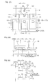
FIG.4A to FIG.4D are schematic views for explaining configuration and write operation of a conventional FLOTOX EEPROM. Out of these figures,FIG.4A and FIG.4C are plan views of this EEPROM.FIG.4B is a sectional view taken along the line B-B inFIG.4A , showing a cross section structure of the EEPROM.FIG.4D is a sectional view taken along the line D-D inFIG. 4C , showing the cross section structure. - In
FIG.4A to FIG.4D , floating gates arranged in array are indicated at 1 while tunnel windows associated with the respective floating gates are indicated at 2. Indicated at 3 is a select gate shared by the plural floating gates, and a control gate shared by the plural floating gates is indicated at 4. Indicated at 5 is a source shared by the plural floating gates, while drains provided in one-on-one correspondence to the plural control gates are indicated at 6. These components are formed on a surface layer region of a p-type silicon substrate. - In a write operation of the conventional EEPROM shown in
FIG.4A to FIG.4D , data is written by collectively injecting electrons into thefloating gates 1 in units of bytes, followed by selectively extracting electrons from the cells. Specifically, as shown inFIG.4A and FIG.4B , the individual floating gates 1 (AlthoughFIG.4A shows only threefloating gates 1, actual voltage application is collectively controlled on a byte-by-byte basis or in units of eight floating gates) and the sharedsource 5 are opened, while the ground potential is applied to theplural drains 6 and a voltage Vpp (Vpp represents a write voltage which is a high voltage of 15 to 17V) is applied to the sharedcontrol gate 4 and the sharedselect gate 3. This causes electrons to be injected from eachdrain 6 to eachfloating gate 1 via each tunnel window 2 (seeFIG.4B ).
On the other hand, when electrons injected into thefloating gate 1 are extracted, the ground potential is applied to the sharedcontrol gate 4 while the voltage Vpp is selectively applied to theselect gate 3 and anydrain 6 corresponding to afloating gate 1 which extracts electrons, as shown inFIG.4C andFIG.4D . This causes electrons to be extracted from thefloating gate 1 corresponding to thedrain 6 applied with the voltage Vpp and to flow to thedrain 6 via the tunnel window 2 (seeFIG.4D ).
More recently, both the chip size and the memory cell size are reduced, as described above. Therefore, the reduced isolation distance requires increasing of field inversion voltage and hence, the channel stopper is increased in impurity concentration. Since the drain area is also reduced, it is difficult to secure a sufficient distance between the drain junction and the channel stopper region. This leads to a problem that the drain breakdown voltage is lowered to disable the application of an adequately high write voltage Vpp. - More specifically, as shown in
FIG.5 , thedrain region 6 is formed at a region isolated byLOCOS oxides 8 formed in the surface layer region of the p-type silicon substrate 7 by a LOCOS process, for example. Ap+ region 9, which is called achannel stopper 9 having high impurity concentration, is formed under theLOCOS oxide 8 so as to increase isolation breakdown voltage. However, there is a problem that unless a givendistance 10 is secured between the channel stopperregion 9 and the drain (drain junction region) 6, the breakdown voltage of the EEPROM is lowered so that a required voltage for writing data cannot be applied to thedrain 6. This makes the EEPROM unable to serve as a memory. - In view of the foregoing, the present invention has a primary object to provide a FLOTOX EEPROM comprising an EEPROM which can be increased in the drain breakdown voltage so as to allow the setting of high write voltage and which is reduced in cell area.
Another object of the invention is to provide a FLOTOX EEPROM which can make a great difference between threshold voltages for electron injection into the floating gate and for electron extraction from the floating gate, achieving the high reliability design. - A still another object of the invention is to provide a FLOTOX EEPROM wherein the drain is shared by the plural floating gates so as to increase the junction breakdown voltage of the drain region.
Yet another object of the invention is to provide a FLOTOX EEPROM wherein erase and write operations are reverse from those of the conventional EEPROM. - According to the invention for achieving the above objects, the FLOTOX EEPROM comprises: a plurality of floating gates (11) arranged in array, each having a tunnel window (12) and allowing electron injection and extraction via the tunnel window (12); a plurality of select gates (13) provided in one-on-one correspondence to the plural floating gates (11); a control gate (16) shared by the plural floating gates (11); a source (17) shared by the plural floating gates (11); and a drain (18) shared by the plural floating gates (11).
- The alphanumeric characters in parentheses represent corresponding components and the like of an embodiment to be described hereinlater. However, the alphanumeric characters do not mean to limit the scope of the invention. Hereinafter, the same holds for this term.
According to this configuration, the drain (18) is shared by the plural floating gates (11). The drain (18) shared by the plural floating gates (11) can be increased in the area so as to be able to secure a given area as a drain region although the whole body of memory cell is decreased in size. Hence, the drain (18) can attain a high breakdown voltage at its junction. As a result, a great difference can be provided between the threshold voltages for erasure and writing. - Since the select gates (13) are provided in one-on-one correspondence to the floating gates (11), the select gate (13) is made accessible as a bit line (15) by providing a contact at each of the select gates
(13).
In such a case, it is preferable to form the contact (14) at a gate on active plane in order to reduce the cell area. It is desirable that each of the plural select gates (13) has a W-polyside structure such as to reduce influence on a substrate. - The FLOTOX EEPROM of the invention may be provided with the plural floating gates (11) and select gates (13) in units of eight pieces.
According to the configuration, electrons can be collectively extracted from the eight floating gates (11) on a byte-by-byte basis. Subsequently, electrons are selectively injected into the floating gates (11) whereby memory write control can be accomplished on a byte-by-byte basis. - The FLOTOX EEPROM of the invention may be configured such that the plural select gates (13) are respectively connected with discrete bit lines (15) and that the drain (18) is connected with a word line (20) shared by the plural floating gates (11).
This configuration can provide a FLOTOX EEPROM featuring write and erase operations reverse from those of the conventional FLOTOX EEPROM. - In accordance with the invention, a method of writing data to the FLOTOX EEPROM according to any one of the above aspects of the invention is characterized in that data is written by collectively extracting electrons from the plural floating gates (11), followed by selectively injecting electrons into the plural floating gates (11).
The method of writing data according to another aspect of the invention is characterized in that electrons are collectively extracted from the plural floating gates (11) by opening the source (17) of the EEPROM, setting the voltage of a substrate (21) to the ground potential, and applying 0V to the control gate (16) and a high voltage to the select gates (13) and the drain (18), and that electrons are injected into the floating gates (11) by opening the source (17) of the EEPROM, setting the voltage of the substrate (21) to the ground potential, applying 0V to the drain (18) and selectively applying a high voltage to the control gate (16) and any select gate (13) corresponding to a floating gate (11) electron injection to which is desired. - These methods of the invention can set a high write voltage and can make a great difference between the threshold voltages for erasing data from or writing data to the EEPROM.
The above and other objects, features and effects of the present invention will become apparent from the following description of the embodiment thereof made with reference to the accompanying drawings. -
- [
FIG.1A ] A schematic plan view for explaining a configuration of a FLOTOX EEPROM according to an embodiment of the invention. - [
FIG.1B ] A schematic sectional view for explaining the configuration of the FLOTOX EEPROM according to the embodiment of the invention. - [
FIG.2A ] A view for explaining an operation of the FLOTOX EEPROM according to the embodiment of the invention, showing a manner of applying voltage to erase data. - [
FIG.2B ] A view for explaining the operation of the FLOTOX EEPROM according to the embodiment of the invention, showing the manner of applying voltage to erase data. - [
FIG.2C ] A view for explaining the operation of the FLOTOX EEPROM according to the embodiment of the invention, showing the manner of applying voltage to erase data. - [
FIG.3A ] A view for explaining an operation of the FLOTOX EEPROM according to the embodiment of the invention, showing a manner of applying voltage to write data. - [
FIG.3B ] A view for explaining the operation of the FLOTOX EEPROM according to the embodiment of the invention, showing the manner of applying voltage to write data. - [
FIG.3C ] A view for explaining the operation of the FLOTOX EEPROM according to the embodiment of the invention, showing the manner of applying voltage to write data. - [
FIG.4A ] A schematic view for explaining configuration and write operation of a conventional FLOTOX EEPROM. - [
FIG.4B ] A schematic view for explaining the configuration and write operation of the conventional FLOTOX EEPROM. - [
FIG.4C ] A schematic view for explaining the configuration and write operation of the conventional FLOTOX EEPROM. - [
FIG.4D ] A schematic view for explaining the configuration and write operation of the conventional FLOTOX EEPROM. - [
FIG.5 ] A sectional view for explaining a distance required for drain breakdown voltage of the conventional FLOTOX EEPROM. -
- 11:
- Floating gate
- 12:
- Tunnel window
- 13:
- Select gate
- 14:
- Contact
- 15:
- Bit line
- 16:
- Control gate
- 17:
- Source
- 18:
- Drain
- 19:
- Contact
- 20:
- Word line
- An embodiment of the invention will be described in detail as below with reference to the accompanying drawings.
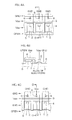
FIG.1A is a schematic plan view for explaining a configuration of a FLOTOX EEPROM according to an embodiment of the invention.FIG.1B is a schematic sectional view taken along the line B-B inFIG.1A , showing a cross section structure of the FLOTOX EEPROM.
InFIG.1A and FIG.1B , indicated at 11 are floating gates arranged in array. WhileFIG.1A shows four floating gates arranged in a transverse direction, the floatinggates 11 are actually arranged on a byte-by-byte basis. Namely, the floating gates are arranged in units of eight pieces. Indicated at 12 are tunnel windows provided in association with the respective floating gates. Indicated at 13 are select gates provided in correspondence to the respective floatinggates 11. Each of theselect gates 13 is connected with adiscrete bit line 15 via acontact 14. Indicated at 16 is a control gate shared by the plural (normally eight) floatinggates 11, while a source shared by the plural (normally eight) floatinggates 11 is indicated at 17. A drain shared by the plural (normally eight) floatinggates 11 is indicated at 18. As shown in the figure, the drain is shared thereby securing a comparativelylarge drain region 18. Thedrain 18 is connected with aword line 20 via acontact 19. - Each of the
select gates 13 provided in correspondence to each floatinggate 11 has thecontact 14 formed at a gate on active plane. In order to reduce influence on a substrate, theselect gate 13 and thecontrol gate 16 adopt a W-polyside structure as shown inFIG.1B .
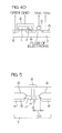
FIG.2A to FIG.2C andFIG.3A to FIG.3C are views for explaining an operation of the FLOTOX EEPROM according to the embodiment of the invention.FIG.2A to FIG.2C show a manner of applying voltage to erase data whileFIG.3A to FIG.3C show a manner of applying voltage to write data. -
FIG.2A is a plan view of the EEPROM.FIG.2B is a sectional view taken along the line B-B inFIG.2A .
FIG.2C is a schematic view showing circuitry ofFIG.2A . AlthoughFIG.2A to FIG.2C show a 3-cell configuration (configuration including three floating gates 11), the application of voltage to the floatinggates 11 is actually controlled on a byte-by-byte basis, namely in units of eight pieces.
In data erasure, thesource 17 is opened, the voltage of asubstrate 21 is set to the ground potential, 0V is applied to thecontrol gate 16 and a high voltage of 15 to 17V is applied to the individualselect gates 13 and the shareddrain 18. This causes electrons to be extracted from the individual floatinggates 11 to thedrain 18. This voltage application operation is collectively performed on all the cells (floating gates 11) in units of bytes. Namely, the process of extracting electrons from the plural floating gates is collectively performed on a byte-by-byte basis. - Next, a data write operation is described with reference to
FIG.3A to FIG.3C. FIG.3A is a plan view of the EEPROM.FIG.3B is a sectional view taken along the line B-B inFIG.3A. FIG.3C is a schematic view showing circuitry ofFIG.3A .
Thesource 17 is opened while thesubstrate 21 is set to the ground potential. Then, 0V is applied to the shareddrain 18, while a high voltage of 15 to 17V is applied to the sharedcontrol gate 16. Further, a high voltage of 15 to 17V is applied only to aselect gate 13 corresponding to a floatinggate 11 the write operation to which is desired, while 0V is applied to aselect gate 13 corresponding to a floatinggate 11 which does not require the write operation. Thus, electrons are injected only into the floatinggate 11 corresponding to theselect gate 13 applied with the high voltage, so as to accomplish the write operation. In this manner, the EEPROM according to the embodiment allows electrons to be injected only into the desired floating gate by controlling the voltage application to theselect gates 13 provided in correspondence to the floatinggates 11. - When written data is read from the EEPROM with data written to it, a voltage of about 1V, for example, is applied to the
control gate 16 and a sense voltage of about 3 to 5V is applied to the individualselect gates 13 and the shareddrain 18 whereby electric current is not passed through the floatinggate 11 injected with electrons but is passed through the floatinggate 11 free from injection of electrons. Thus, the data can be read out. - The invention is not limited to the teachings of the embodiment described above, and various changes or modifications may be made thereto within the scope of the claims thereof.
For instance, the above embodiment illustrates the voltage application to the cells (floating gates 11) which is controlled in units of eight pieces but not limited to this. The voltage application may be controlled, for example, in units of four floating gates or of two floating gates. Alternatively, the voltage application may be controlled in units of 16 floating gates. - The present application is based on Japanese Patent Application No.
2007-098301
Claims (5)
- A FLOTOX EEPROM comprising:a plurality of floating gates arranged in array, each having a tunnel window and allowing electron injection and extraction via the tunnel window;a plurality of select gates provided in one-on-one correspondence to the plural floating gates;a control gate shared by the plural floating gates;a source shared by the plural floating gates; anda drain shared by the plural floating gates.
- The FLOTOX EEPROM according to Claim 1, wherein the plural floating gates and select gates are provided in units of eight pieces.
- The FLOTOX EEPROM according to Claim 1 or 2, wherein the plural select gates are respectively connected with discrete bit lines, and
the drain is connected with a word line shared by the plural floating gates. - A method of writing data to the FLOTOX EEPROM according to any one of Claims 1 to 3, wherein data is written by collectively extracting electrons from the plural floating gates, followed by selectively injecting electrons into the plural floating gates.
- The method of writing data according to Claim 4, wherein electrons are collectively extracted from the plural floating gates by opening the source of the EEPROM, setting the voltage of a substrate to the ground potential, and applying 0V to the control gate and a high voltage to the select gates and the drain, and
electrons are injected into the floating gates by opening the source of the EEPROM, setting the voltage of the substrate to the ground potential, applying 0V to the drain and selectively applying a high voltage to the control gate and any select gate corresponding to a floating gate electron injection to which is desired.
Applications Claiming Priority (2)
| Application Number | Priority Date | Filing Date | Title |
|---|---|---|---|
| JP2007098301A JP5112731B2 (en) | 2007-04-04 | 2007-04-04 | FLOTOX EEPROM |
| PCT/JP2008/056584 WO2008123548A1 (en) | 2007-04-04 | 2008-04-02 | Flotox type eeprom |
Publications (2)
| Publication Number | Publication Date |
|---|---|
| EP2136397A1 true EP2136397A1 (en) | 2009-12-23 |
| EP2136397A4 EP2136397A4 (en) | 2011-05-25 |
Family
ID=39831021
Family Applications (1)
| Application Number | Title | Priority Date | Filing Date |
|---|---|---|---|
| EP08739695A Withdrawn EP2136397A4 (en) | 2007-04-04 | 2008-04-02 | FLOTOX TYPE EEPROM |
Country Status (5)
| Country | Link |
|---|---|
| US (1) | US8072807B2 (en) |
| EP (1) | EP2136397A4 (en) |
| JP (1) | JP5112731B2 (en) |
| TW (1) | TWI499040B (en) |
| WO (1) | WO2008123548A1 (en) |
Families Citing this family (2)
| Publication number | Priority date | Publication date | Assignee | Title |
|---|---|---|---|---|
| US20120063223A1 (en) * | 2010-09-09 | 2012-03-15 | Aplus Flash Technology, Inc. | Most compact flotox-based combo NVM design without sacrificing EEPROM endurance cycles for 1-die data and code storage |
| US8383475B2 (en) * | 2010-09-23 | 2013-02-26 | Globalfoundries Singapore Pte. Ltd. | EEPROM cell |
Family Cites Families (15)
| Publication number | Priority date | Publication date | Assignee | Title |
|---|---|---|---|---|
| EP0459164B1 (en) * | 1990-06-01 | 1996-09-04 | Texas Instruments Incorporated | Erasable programmable memory |
| JPH04123471A (en) * | 1990-09-14 | 1992-04-23 | Oki Electric Ind Co Ltd | Writing and erasing method for data of semiconductor memory |
| JPH04364077A (en) * | 1991-06-11 | 1992-12-16 | Toshiba Corp | Non-volatile semiconductor storage element and non-volatile semiconductor storage device |
| US5218568A (en) * | 1991-12-17 | 1993-06-08 | Texas Instruments Incorporated | Electrically-erasable, electrically-programmable read-only memory cell, an array of such cells and methods for making and using the same |
| US5284786A (en) * | 1992-08-14 | 1994-02-08 | National Semiconductor Corporation | Method of making a split floating gate EEPROM cell |
| US5404037A (en) * | 1994-03-17 | 1995-04-04 | National Semiconductor Corporation | EEPROM cell with the drain diffusion region self-aligned to the tunnel oxide region |
| JPH0936335A (en) * | 1995-07-14 | 1997-02-07 | Nkk Corp | Nonvolatile semiconductor memory device |
| JP2005183763A (en) * | 2003-12-22 | 2005-07-07 | Toshiba Microelectronics Corp | Manufacturing method of semiconductor device including nonvolatile memory |
| US6878991B1 (en) * | 2004-01-30 | 2005-04-12 | Micron Technology, Inc. | Vertical device 4F2 EEPROM memory |
| JP2005005731A (en) | 2004-08-20 | 2005-01-06 | Sharp Corp | Semiconductor memory device |
| US7642594B2 (en) * | 2005-07-25 | 2010-01-05 | Freescale Semiconductor, Inc | Electronic device including gate lines, bit lines, or a combination thereof |
| JP2007098301A (en) | 2005-10-05 | 2007-04-19 | Tadahiro Fujii | Continuous soil washing and discharge method |
| FR2901626A1 (en) * | 2006-05-29 | 2007-11-30 | St Microelectronics Sa | Memory cell programming or erasing method for electrically EPROM, involves applying non-zero compensation voltage to gate of MOS transistor, and applying inhibiting voltage to gate or source of floating gate transistor |
| JP2007013197A (en) | 2006-08-24 | 2007-01-18 | Renesas Technology Corp | Nonvolatile semiconductor memory device |
| CN101595555A (en) * | 2007-01-29 | 2009-12-02 | 罗姆股份有限公司 | FLOTOX type EEPROM |
-
2007
- 2007-04-04 JP JP2007098301A patent/JP5112731B2/en not_active Expired - Fee Related
-
2008
- 2008-04-02 TW TW097112045A patent/TWI499040B/en not_active IP Right Cessation
- 2008-04-02 US US12/594,751 patent/US8072807B2/en not_active Expired - Fee Related
- 2008-04-02 EP EP08739695A patent/EP2136397A4/en not_active Withdrawn
- 2008-04-02 WO PCT/JP2008/056584 patent/WO2008123548A1/en not_active Ceased
Also Published As
| Publication number | Publication date |
|---|---|
| TW200903783A (en) | 2009-01-16 |
| TWI499040B (en) | 2015-09-01 |
| US20100149878A1 (en) | 2010-06-17 |
| JP2008258364A (en) | 2008-10-23 |
| JP5112731B2 (en) | 2013-01-09 |
| WO2008123548A1 (en) | 2008-10-16 |
| EP2136397A4 (en) | 2011-05-25 |
| US8072807B2 (en) | 2011-12-06 |
Similar Documents
| Publication | Publication Date | Title |
|---|---|---|
| US7688627B2 (en) | Flash memory array of floating gate-based non-volatile memory cells | |
| US5235544A (en) | Flash EPROM cell and method for operating same | |
| US7006381B2 (en) | Semiconductor device having a byte-erasable EEPROM memory | |
| US7903465B2 (en) | Memory array of floating gate-based non-volatile memory cells | |
| EP2043145A1 (en) | Nonvolatile semiconductor memory and its drive method | |
| CN101640067A (en) | Memory cell and array operation method for reducing punch-through leakage | |
| US20070166889A1 (en) | Method of forming a well of a NAND flash memory device | |
| US6952369B2 (en) | Method for operating a NAND-array memory module composed of P-type memory cells | |
| EP2973717B1 (en) | Eeprom memory cell with low voltage read path and high voltage erase/write path | |
| US5998826A (en) | Triple well floating gate memory and operating method with isolated channel program, preprogram and erase processes | |
| JPH06291332A (en) | Semiconductor memory device and method of using the same | |
| US7405972B1 (en) | Non-volatile memory array | |
| US8072807B2 (en) | FLOTOX type EEPROM | |
| CN107658301B (en) | Flash memory unit, flash memory array and operation method thereof | |
| JPH11233743A (en) | Nonvolatile semiconductor memory device | |
| JP2003124362A (en) | Nonvolatile semiconductor memory device and driving method thereof | |
| EP2109136A1 (en) | Flotox-type eeprom | |
| US5787035A (en) | Memory cell array | |
| US6049483A (en) | Nonvolatile memory device having program and/or erase voltage clamp | |
| JP5073318B2 (en) | FLOTOX EEPROM | |
| JPH11273387A (en) | Non-volatile semiconductor memory device | |
| JP2002118187A (en) | Non-volatile semiconductor memory device | |
| JPH01173398A (en) | Non-volatile semiconductor memory device | |
| JPH09148463A (en) | Semiconductor storage device and its driving method | |
| JP2001135088A (en) | Nonvolatile semiconductor memory device |
Legal Events
| Date | Code | Title | Description |
|---|---|---|---|
| PUAI | Public reference made under article 153(3) epc to a published international application that has entered the european phase |
Free format text: ORIGINAL CODE: 0009012 |
|
| 17P | Request for examination filed |
Effective date: 20091015 |
|
| AK | Designated contracting states |
Kind code of ref document: A1 Designated state(s): AT BE BG CH CY CZ DE DK EE ES FI FR GB GR HR HU IE IS IT LI LT LU LV MC MT NL NO PL PT RO SE SI SK TR |
|
| DAX | Request for extension of the european patent (deleted) | ||
| A4 | Supplementary search report drawn up and despatched |
Effective date: 20110427 |
|
| RIC1 | Information provided on ipc code assigned before grant |
Ipc: H01L 29/788 20060101ALI20110419BHEP Ipc: H01L 27/115 20060101ALI20110419BHEP Ipc: H01L 21/8247 20060101AFI20081028BHEP Ipc: G11C 16/04 20060101ALI20110419BHEP |
|
| 17Q | First examination report despatched |
Effective date: 20120423 |
|
| STAA | Information on the status of an ep patent application or granted ep patent |
Free format text: STATUS: THE APPLICATION IS DEEMED TO BE WITHDRAWN |
|
| 18D | Application deemed to be withdrawn |
Effective date: 20120904 |