EP2120252A1 - Plasmaanzeigetafel - Google Patents
Plasmaanzeigetafel Download PDFInfo
- Publication number
- EP2120252A1 EP2120252A1 EP09701468A EP09701468A EP2120252A1 EP 2120252 A1 EP2120252 A1 EP 2120252A1 EP 09701468 A EP09701468 A EP 09701468A EP 09701468 A EP09701468 A EP 09701468A EP 2120252 A1 EP2120252 A1 EP 2120252A1
- Authority
- EP
- European Patent Office
- Prior art keywords
- dielectric layer
- barrier ribs
- pdp
- oxide
- base film
- Prior art date
- Legal status (The legal status is an assumption and is not a legal conclusion. Google has not performed a legal analysis and makes no representation as to the accuracy of the status listed.)
- Withdrawn
Links
Images


Classifications
-
- H—ELECTRICITY
- H01—ELECTRIC ELEMENTS
- H01J—ELECTRIC DISCHARGE TUBES OR DISCHARGE LAMPS
- H01J11/00—Gas-filled discharge tubes with alternating current induction of the discharge, e.g. alternating current plasma display panels [AC-PDP]; Gas-filled discharge tubes without any main electrode inside the vessel; Gas-filled discharge tubes with at least one main electrode outside the vessel
- H01J11/20—Constructional details
- H01J11/34—Vessels, containers or parts thereof, e.g. substrates
- H01J11/40—Layers for protecting or enhancing the electron emission, e.g. MgO layers
-
- H—ELECTRICITY
- H01—ELECTRIC ELEMENTS
- H01J—ELECTRIC DISCHARGE TUBES OR DISCHARGE LAMPS
- H01J11/00—Gas-filled discharge tubes with alternating current induction of the discharge, e.g. alternating current plasma display panels [AC-PDP]; Gas-filled discharge tubes without any main electrode inside the vessel; Gas-filled discharge tubes with at least one main electrode outside the vessel
- H01J11/10—AC-PDPs with at least one main electrode being out of contact with the plasma
- H01J11/12—AC-PDPs with at least one main electrode being out of contact with the plasma with main electrodes provided on both sides of the discharge space
-
- H—ELECTRICITY
- H01—ELECTRIC ELEMENTS
- H01J—ELECTRIC DISCHARGE TUBES OR DISCHARGE LAMPS
- H01J11/00—Gas-filled discharge tubes with alternating current induction of the discharge, e.g. alternating current plasma display panels [AC-PDP]; Gas-filled discharge tubes without any main electrode inside the vessel; Gas-filled discharge tubes with at least one main electrode outside the vessel
- H01J11/20—Constructional details
- H01J11/34—Vessels, containers or parts thereof, e.g. substrates
- H01J11/36—Spacers, barriers, ribs, partitions or the like
Definitions
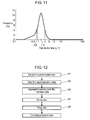
- trial product 4 when a cathode luminescence of the crystal particles attached to the base film is measured, trial product 4 has a property of emission intensity with respect to wavelength shown in Fig. 7 .
- the emission intensity is represented by relative values.
Landscapes
- Physics & Mathematics (AREA)
- Engineering & Computer Science (AREA)
- Plasma & Fusion (AREA)
- Gas-Filled Discharge Tubes (AREA)
Applications Claiming Priority (2)
| Application Number | Priority Date | Filing Date | Title |
|---|---|---|---|
| JP2008058927A JP5298578B2 (ja) | 2008-03-10 | 2008-03-10 | プラズマディスプレイパネル |
| PCT/JP2009/000838 WO2009113254A1 (ja) | 2008-03-10 | 2009-02-26 | プラズマディスプレイパネル |
Publications (2)
| Publication Number | Publication Date |
|---|---|
| EP2120252A1 true EP2120252A1 (de) | 2009-11-18 |
| EP2120252A4 EP2120252A4 (de) | 2011-02-16 |
Family
ID=41064927
Family Applications (1)
| Application Number | Title | Priority Date | Filing Date |
|---|---|---|---|
| EP09701468A Withdrawn EP2120252A4 (de) | 2008-03-10 | 2009-02-26 | Plasmaanzeigetafel |
Country Status (6)
| Country | Link |
|---|---|
| US (1) | US8164262B2 (de) |
| EP (1) | EP2120252A4 (de) |
| JP (1) | JP5298578B2 (de) |
| KR (1) | KR101148453B1 (de) |
| CN (1) | CN101896989A (de) |
| WO (1) | WO2009113254A1 (de) |
Families Citing this family (1)
| Publication number | Priority date | Publication date | Assignee | Title |
|---|---|---|---|---|
| JP4399344B2 (ja) * | 2004-11-22 | 2010-01-13 | パナソニック株式会社 | プラズマディスプレイパネルおよびその製造方法 |
Family Cites Families (14)
| Publication number | Priority date | Publication date | Assignee | Title |
|---|---|---|---|---|
| JP3705914B2 (ja) * | 1998-01-27 | 2005-10-12 | 三菱電機株式会社 | 面放電型プラズマディスプレイパネル及びその製造方法 |
| JP4541832B2 (ja) * | 2004-03-19 | 2010-09-08 | パナソニック株式会社 | プラズマディスプレイパネル |
| JP4399344B2 (ja) * | 2004-11-22 | 2010-01-13 | パナソニック株式会社 | プラズマディスプレイパネルおよびその製造方法 |
| JP4611057B2 (ja) * | 2005-03-01 | 2011-01-12 | 宇部マテリアルズ株式会社 | 交流型プラズマディスプレイパネルの誘電体層保護膜形成用の酸化マグネシウム微粒子分散液 |
| JP4839937B2 (ja) | 2005-07-14 | 2011-12-21 | パナソニック株式会社 | 酸化マグネシウム原材料およびプラズマディスプレイパネルの製造方法 |
| JP4089733B2 (ja) * | 2006-02-14 | 2008-05-28 | 松下電器産業株式会社 | プラズマディスプレイパネル |
| CN101479827B (zh) * | 2006-04-28 | 2012-06-13 | 松下电器产业株式会社 | 等离子显示面板及其制造方法 |
| JP4774329B2 (ja) * | 2006-05-16 | 2011-09-14 | パナソニック株式会社 | プラズマディスプレイパネル |
| JP2008293772A (ja) | 2007-05-24 | 2008-12-04 | Panasonic Corp | プラズマディスプレイパネル及びその製造方法、並びにプラズマディスプレイパネル |
| JP2009129616A (ja) * | 2007-11-21 | 2009-06-11 | Panasonic Corp | プラズマディスプレイパネル |
| JP2009211864A (ja) * | 2008-03-03 | 2009-09-17 | Panasonic Corp | プラズマディスプレイパネル |
| JP2009252482A (ja) * | 2008-04-04 | 2009-10-29 | Panasonic Corp | プラズマディスプレイパネル |
| KR20120023053A (ko) * | 2010-02-12 | 2012-03-12 | 파나소닉 주식회사 | 플라즈마 디스플레이 패널의 제조 방법 |
| JPWO2011114672A1 (ja) * | 2010-03-18 | 2013-06-27 | パナソニック株式会社 | プラズマディスプレイ装置 |
-
2008
- 2008-03-10 JP JP2008058927A patent/JP5298578B2/ja not_active Expired - Fee Related
-
2009
- 2009-02-26 EP EP09701468A patent/EP2120252A4/de not_active Withdrawn
- 2009-02-26 WO PCT/JP2009/000838 patent/WO2009113254A1/ja not_active Ceased
- 2009-02-26 KR KR1020097019669A patent/KR101148453B1/ko not_active Expired - Fee Related
- 2009-02-26 US US12/526,648 patent/US8164262B2/en not_active Expired - Fee Related
- 2009-02-26 CN CN2009801003593A patent/CN101896989A/zh active Pending
Also Published As
| Publication number | Publication date |
|---|---|
| WO2009113254A1 (ja) | 2009-09-17 |
| CN101896989A (zh) | 2010-11-24 |
| US20110198993A1 (en) | 2011-08-18 |
| US8164262B2 (en) | 2012-04-24 |
| KR101148453B1 (ko) | 2012-05-25 |
| JP5298578B2 (ja) | 2013-09-25 |
| EP2120252A4 (de) | 2011-02-16 |
| JP2009218020A (ja) | 2009-09-24 |
| KR20090122358A (ko) | 2009-11-27 |
Similar Documents
| Publication | Publication Date | Title |
|---|---|---|
| EP2214193B1 (de) | Plasmaanzeigetafel | |
| US8395320B2 (en) | Plasma display panel | |
| EP2101342A1 (de) | Plasmaanzeigetafel | |
| EP2099051B1 (de) | Plasmaanzeigetafel | |
| EP2120251A1 (de) | Plasmaanzeigetafel | |
| US8143786B2 (en) | Plasma display panel | |
| US7994718B2 (en) | Plasma display panel | |
| EP2124241B1 (de) | Plasmaanzeigetafel | |
| EP2099049A1 (de) | Verfahren zur herstellung einer plasmaanzeigetafel | |
| US8164262B2 (en) | Plasma display panel | |
| US8053989B2 (en) | Plasma display panel | |
| US8198813B2 (en) | Plasma display panel | |
| EP2141726B1 (de) | Plasmaanzeigetafel | |
| EP2141727A1 (de) | Plasmaanzeigetafel | |
| EP2136385A1 (de) | Verfahren zur herstellung einer plasmaanzeigetafel |
Legal Events
| Date | Code | Title | Description |
|---|---|---|---|
| PUAI | Public reference made under article 153(3) epc to a published international application that has entered the european phase |
Free format text: ORIGINAL CODE: 0009012 |
|
| 17P | Request for examination filed |
Effective date: 20090720 |
|
| AK | Designated contracting states |
Kind code of ref document: A1 Designated state(s): AT BE BG CH CY CZ DE DK EE ES FI FR GB GR HR HU IE IS IT LI LT LU LV MC MK MT NL NO PL PT RO SE SI SK TR |
|
| RIN1 | Information on inventor provided before grant (corrected) |
Inventor name: OOE, YOSHINAO Inventor name: SAKAMOTO, KOYO Inventor name: UETANI, KAZUO Inventor name: SHIOKAWA, AKIRA Inventor name: MIZOKAMI, KANAME Inventor name: ISHINO, SHINICHIRO Inventor name: KADO, HIROYUKI Inventor name: KAWARAZAKI, HIDEJI |
|
| A4 | Supplementary search report drawn up and despatched |
Effective date: 20110119 |
|
| RIC1 | Information provided on ipc code assigned before grant |
Ipc: H01J 17/49 20060101AFI20110113BHEP |
|
| DAX | Request for extension of the european patent (deleted) | ||
| STAA | Information on the status of an ep patent application or granted ep patent |
Free format text: STATUS: THE APPLICATION IS DEEMED TO BE WITHDRAWN |
|
| 18D | Application deemed to be withdrawn |
Effective date: 20130903 |