EP2110834B1 - Touch switch structure - Google Patents
Touch switch structure Download PDFInfo
- Publication number
- EP2110834B1 EP2110834B1 EP08710615.9A EP08710615A EP2110834B1 EP 2110834 B1 EP2110834 B1 EP 2110834B1 EP 08710615 A EP08710615 A EP 08710615A EP 2110834 B1 EP2110834 B1 EP 2110834B1
- Authority
- EP
- European Patent Office
- Prior art keywords
- base material
- touch
- touch switch
- electrode layer
- shield electrode
- Prior art date
- Legal status (The legal status is an assumption and is not a legal conclusion. Google has not performed a legal analysis and makes no representation as to the accuracy of the status listed.)
- Not-in-force
Links
Images

Classifications
-
- B—PERFORMING OPERATIONS; TRANSPORTING
- B60—VEHICLES IN GENERAL
- B60H—ARRANGEMENTS OF HEATING, COOLING, VENTILATING OR OTHER AIR-TREATING DEVICES SPECIALLY ADAPTED FOR PASSENGER OR GOODS SPACES OF VEHICLES
- B60H1/00—Heating, cooling or ventilating [HVAC] devices
- B60H1/00642—Control systems or circuits; Control members or indication devices for heating, cooling or ventilating devices
- B60H1/0065—Control members, e.g. levers or knobs
-
- B—PERFORMING OPERATIONS; TRANSPORTING
- B60—VEHICLES IN GENERAL
- B60R—VEHICLES, VEHICLE FITTINGS, OR VEHICLE PARTS, NOT OTHERWISE PROVIDED FOR
- B60R16/00—Electric or fluid circuits specially adapted for vehicles and not otherwise provided for; Arrangement of elements of electric or fluid circuits specially adapted for vehicles and not otherwise provided for
- B60R16/005—Electro-mechanical devices, e.g. switched
-
- H—ELECTRICITY
- H03—ELECTRONIC CIRCUITRY
- H03K—PULSE TECHNIQUE
- H03K17/00—Electronic switching or gating, i.e. not by contact-making and –breaking
- H03K17/94—Electronic switching or gating, i.e. not by contact-making and –breaking characterised by the way in which the control signals are generated
- H03K17/96—Touch switches
- H03K17/962—Capacitive touch switches
-
- H—ELECTRICITY
- H01—ELECTRIC ELEMENTS
- H01H—ELECTRIC SWITCHES; RELAYS; SELECTORS; EMERGENCY PROTECTIVE DEVICES
- H01H2239/00—Miscellaneous
- H01H2239/006—Containing a capacitive switch or usable as such
-
- H—ELECTRICITY
- H01—ELECTRIC ELEMENTS
- H01H—ELECTRIC SWITCHES; RELAYS; SELECTORS; EMERGENCY PROTECTIVE DEVICES
- H01H2239/00—Miscellaneous
- H01H2239/03—Avoiding erroneous switching
-
- H—ELECTRICITY
- H03—ELECTRONIC CIRCUITRY
- H03K—PULSE TECHNIQUE
- H03K17/00—Electronic switching or gating, i.e. not by contact-making and –breaking
- H03K17/94—Electronic switching or gating, i.e. not by contact-making and –breaking characterised by the way in which the control signals are generated
- H03K17/96—Touch switches
- H03K2017/9602—Touch switches characterised by the type or shape of the sensing electrodes
- H03K2017/9604—Touch switches characterised by the type or shape of the sensing electrodes characterised by the number of electrodes
- H03K2017/9606—Touch switches characterised by the type or shape of the sensing electrodes characterised by the number of electrodes using one electrode only per touch switch
Definitions
- the present invention relates to a capacitance-type touch switch structure that senses an approach or a touch of a finger or a hand by a change in capacitance between electrodes. Particularly, it relates to a touch switch structure that can be preferably used for an automotive instrument panel.
- touch switches have been widely known which detect a human body part touching on or approaching to a conductive electrode member and trigger a desired instrument.
- the electrode member functions as a capacitance sensor which detects on-off of the touch switch by reading change in impedance (capacitance) of the electrode when a human body touches the electrode.
- Examples of such a capacitance type touch switch include: one in which an electrode, a connection pattern (wiring portion), a conductive thin film and the like are formed by spattering in the form of films (for example, refer to JP-A-2005-38739 ); and one in which an electrode, a connection pattern, a conductive thin film and the like are formed on a base material by screen printing with a conductive ink.
- Such touch switches can be used for automotive instrument panels. Specifically, they can be used as automotive switches such as on-off switches of audio systems or air conditioners, and selector switches switching between various modes. In such cases, if the electrode member is formed on a light-transmissible base material, the switch can be light-transmissible itself while the light is lit and thus enhances the viewability thereof, which maintains the usability even in the nighttime.
- an adjacent touch switch may reacts, for example when a plurality of touch switches are provided.
- US 2005/0264304A discloses an electrical capacitance proximity sensor with high detector sensitivity having an insulating substrate, a detector electrode and an earth electrode formed in a fixed pattern on one face of the insulating substrate, and a detector circuit which detects an object approaching the detector electrode and the earth electrode by detecting the capacitance between the detector electrode and the earth electrode.
- the present invention has been made in view of such problems, and the object thereof is to provide a touch switch structure that securely prevents misjudgments and incorrect detections with respect to operations on the switch.
- the object at above can be achieved by the features specified in the claims.
- FIG. 1 is a schematic plan view of the structure thereof
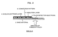
- FIG. 2 is an A-A sectional view of FIG. 1
- the touch switch 1 is provided inside an automobile and applied mainly to an operation panel of an audio system or an air conditioner. Therefore, the base material 2 of the touch switch 1 is formed of a sheet-shaped resin such as polycarbonate or acrylic resin. By forming the base material 2 into thin sheet in this way, the touch switch 1 can be formed into a complicated, curved form.
- forming the base material 2 into thin sheet secures the light-transmission property of the base material 2, which makes it possible to enhance the viewability, usability and design. Namely, when the lights are lit in the nighttime, light from a back-lighting (not shown in the drawings), which is provided on the backside of the base material 2, penetrates the base material 2 just like the touch switch 1 itself emits light. In this way, the design, usability and the like can be improved.
- the base material 2 is formed of a resin in the present embodiment, the material of which the base material 2 is formed is by no means limited to resins insofar as it is nonconductive.
- a touch detection electrode hereinafter abbreviated simply as "sensing electrode" 3
- shield electrode layer 4 On a surface (which corresponds to the upper surface side in FIG. 2 ) of this base material 2, there are provided a touch detection electrode (hereinafter abbreviated simply as "sensing electrode") 3, a shield electrode layer 4 and a insulation layer 5.
- sensing electrode 3 and insulation layer 5 are formed on the base material 2 by means of screen printing. Specifically, the sensing electrode 3 and the shield electrode layer 4 are printed on the base material 2 using an ink containing a conductive material. In addition, the insulation layer 5 is printed on the base material 2 using a nonconductive ink.
- the shield electrode layer 4 is printed at the portion other than where the sensing electrode 3 is formed, as shown in FIG. 1 and FIG. 2 .
- the insulation layer 5 is laminated on the shield electrode layer 4.
- the insulation layer 5 is formed at the portion corresponding to the wiring portion (connection pattern) 6 of the sensing electrode 3 so that the insulation layer 5 is located between the connection pattern 6 and the shield electrode layer 4, as shown in FIG. 2 .
- the insulation layer 5 may have approximately the same area as the shield electrode layer 4 and be formed so that it covers the entire upper surface of the shield electrode layer 4.
- the sensing electrode 3 is formed by coating. Also, the connection pattern 6 is formed on the insulation layer 5. Between the shield electrode layer 4 and the sensing electrode 3, a gap is formed, as shown in FIG. 1 , which prevents direct contact of the shield electrode layer 4 with the sensing electrode 3.
- the connection pattern 6 is disposed, the connection pattern 6, the insulation layer 5, the shield electrode layer 4 and the base material 2 are laminated in the listed order, at the portion where the sensing electrode 3 is disposed, the sensing electrode 3 and the base material 2 are laminated in the listed order, and at the portion where neither the connection pattern 6 nor the sensing electrode 3 is disposed, the shield electrode layer 4 and the base material 2 are laminated in the listed order.
- the sensing electrode 3 is connected to a known detection circuit 7 via the connection pattern 6. Between the detection circuit 7 and the grounding terminal GND, a high-frequency signal source 8 is connected.
- the shield electrode layer 4 is connected between the detection circuit 7 and the high-frequency signal source 8.
- the touch of the operator can be sensed by detecting the change in impedance (change in capacitance) between the detection circuit 7 and the sensing electrode 3, as is the case with the conventional touch switches.
- the electrical sensitivity of the detection circuit 7 is increased in order to detect the operation on the touch switch 1 securely even when the operator wears a glove.
- conventional touch switches may misjudge a touch on a portion other than the sensing electrode 3, for example on the shield electrode layer 4, as a touch on the sensing electrode 3, by reading a slight change in impedance caused between the sensing electrode 3 and the detection circuit 7.
- the direct connection between the shield electrode layer 4 and the high-frequency signal source 8 inhibits change in impedance between the sensing electrode 3 and the detection circuit 7, which makes it possible to prevent the incorrect detection.
- the electrical sensitivity of the detection circuit 7 is increased as described above on the assumption that the operator would wear a glove, and therefore, with a conventional touch switch, a misjudgment may be made because a minute change in impedance may be detected even with just the insulation layer 5.
- the shield electrode layer 4 interposed between the insulation layer 5 and the base material 2 can inhibit change in impedance between the sensing electrode 3 and the detection circuit 7, even when a slight impedance change is detected. Namely, even when the sensitivity of the detection circuit 7 is increased, misjudgments of a touch on the connection pattern 6 as a detection of a touch (on the sensing electrode 3) can be prevented securely.
- the touch switch structure according to one embodiment of the present invention exhibits an advantageous effect of preventing misjudgments and incorrect detections securely during the operation of the touch switch 1 with just a simple structure. Namely, when the fingertip or the like of an operator touches on the sensing electrode 3, that touch of the operator can be sensed by detecting the change in impedance (change in capacitance) between the detection circuit 7 and the sensing electrode 3, as is the case with the conventional touch switches.
- the direct connection between the shield electrode layer 4 and the high-frequency signal source 8 inhibits change in impedance between the sensing electrode 3 and the detection circuit 7, which makes it possible to prevent the incorrect detection. Furthermore, because the sensing electrode 3 is connected via the connection pattern 6 to the detection circuit 7, the high-frequency signal source 8, and the grounding terminal GND in the listed order and the shield electrode layer 4 is directly connected to the high-frequency signal source 8, misjudgments and incorrect detections can be prevented securely even when the sensitivity of the detection circuit 7 is increased.
- shield electrode layer 4 and insulation layer 5 are formed on the base material 2 by printing (screen printing), another advantageous effect of remarkable weight reduction and thickness reduction of the touch switch 1 itself can be achieved .
- the base material 2 is made of a sheet-shaped resin, and therefore, the touch switch 1 can be formed into a complicated, curved form, advantageous effects of heightening flexibility in the place to which the touch switch 1 can be applied and as well as of enhancing the design of the touch switch can be achieved.
- the base material 2 is light-transmissible, viewability and usability when lights are lit in the nighttime, as well as design can be enhanced, by providing a back-lighting or the like on the backside of the touch switch 1.
- the present invention is by no means limited to the above-mentioned embodiment, but various modifications can be added thereto insofar as they do not depart from the scope of the present invention.
- the touch switch is used inside an automobile was described in the above-mentioned embodiment, there is no limitation on where to use the touch switch.
- all of the sensing electrode 3, shield electrode layer 4 and insulation layer 5 are formed by means of screen printing in the above-mentioned embodiment, these can be formed into films by spattering.
Landscapes
- Engineering & Computer Science (AREA)
- Mechanical Engineering (AREA)
- Physics & Mathematics (AREA)
- Thermal Sciences (AREA)
- Switches That Are Operated By Magnetic Or Electric Fields (AREA)
- Air-Conditioning For Vehicles (AREA)
Applications Claiming Priority (2)
| Application Number | Priority Date | Filing Date | Title |
|---|---|---|---|
| JP2007026812A JP4749354B2 (ja) | 2007-02-06 | 2007-02-06 | タッチスイッチ構造 |
| PCT/JP2008/051288 WO2008096639A1 (ja) | 2007-02-06 | 2008-01-29 | タッチスイッチ構造 |
Publications (3)
| Publication Number | Publication Date |
|---|---|
| EP2110834A1 EP2110834A1 (en) | 2009-10-21 |
| EP2110834A4 EP2110834A4 (en) | 2010-07-07 |
| EP2110834B1 true EP2110834B1 (en) | 2013-07-17 |
Family
ID=39681550
Family Applications (1)
| Application Number | Title | Priority Date | Filing Date |
|---|---|---|---|
| EP08710615.9A Not-in-force EP2110834B1 (en) | 2007-02-06 | 2008-01-29 | Touch switch structure |
Country Status (6)
| Country | Link |
|---|---|
| US (1) | US8148659B2 (ja) |
| EP (1) | EP2110834B1 (ja) |
| JP (1) | JP4749354B2 (ja) |
| KR (1) | KR101076954B1 (ja) |
| CN (1) | CN101617378B (ja) |
| WO (1) | WO2008096639A1 (ja) |
Families Citing this family (17)
| Publication number | Priority date | Publication date | Assignee | Title |
|---|---|---|---|---|
| DE102007032851A1 (de) | 2007-02-07 | 2008-08-14 | Johnson Controls Automotive Electronics Gmbh | Kraftfahrzeug-Anzeigeinstrument mit umgreifendem Zeiger |
| DE102007039327B4 (de) | 2007-02-27 | 2017-08-31 | Johnson Controls Automotive Electronics Gmbh | Konisch skaliertes Anzeigeinstrument für ein Kraftfahrzeug und Verfahren zur Montage eines Zeigerinstruments |
| JP5047862B2 (ja) * | 2008-03-31 | 2012-10-10 | 三菱自動車工業株式会社 | パネル装置 |
| KR20110038031A (ko) * | 2008-06-10 | 2011-04-13 | 존슨 컨트롤스 테크놀러지 컴퍼니 | 전도성 잉크/페인트로 만들어진 전기 회로 경로를 구비한 내부 트림 피스 및 생산 프로세스 |
| DE102008049176B4 (de) * | 2008-09-26 | 2011-01-27 | Diehl Ako Stiftung & Co. Kg | Bedienblende für ein Haushaltsgerät sowie Haushaltsgerät mit einer solchen Bedienblende |
| JP2010114015A (ja) * | 2008-11-10 | 2010-05-20 | Futaba Corp | タッチスイッチ部を備えた蛍光表示管および蛍光表示装置 |
| US8219348B2 (en) | 2009-01-22 | 2012-07-10 | Johnson Controls Technology Company | Method for calibrating and/or correcting a display device having a needle, the needle being able to move in rotation about an axis of rotation |
| US8579448B2 (en) | 2010-01-25 | 2013-11-12 | Johnson Controls Technology Company | Pointer structure of an instrument cluster |
| KR101102092B1 (ko) * | 2010-03-24 | 2012-01-04 | 경운대학교 산학협력단 | 정전용량 터치 키의 제조방법 및 이에 의한 정전용량 터치 키 |
| JP5260607B2 (ja) * | 2010-09-01 | 2013-08-14 | 双葉電子工業株式会社 | タッチセンサ及び蛍光表示管 |
| CN103109135B (zh) * | 2010-09-10 | 2015-09-30 | Bsh家用电器有限公司 | 家用电器操作设备 |
| US8736432B2 (en) * | 2011-06-07 | 2014-05-27 | Toyota Motor Engineering & Manufacturing North America, Inc. | Touch sensor having a selectable sensitivity level and method of selecting a sensitivity level of a touch sensor |
| JP2013077555A (ja) * | 2011-09-12 | 2013-04-25 | Futaba Corp | タッチスイッチ |
| LU91942B1 (en) * | 2012-02-10 | 2013-08-12 | Iee Sarl | Capacitive detection device |
| CN107634749A (zh) * | 2017-10-27 | 2018-01-26 | 大明电子有限公司 | 一种导电薄膜及制备方法、装置 |
| CN107719066A (zh) * | 2017-10-27 | 2018-02-23 | 大明电子有限公司 | 一种汽车空调控制装置及触摸生成、控制方法 |
| JP7161983B2 (ja) * | 2019-10-04 | 2022-10-27 | 日立グローバルライフソリューションズ株式会社 | 洗濯機および操作パネル装置 |
Family Cites Families (12)
| Publication number | Priority date | Publication date | Assignee | Title |
|---|---|---|---|---|
| NL184138C (nl) * | 1977-07-30 | 1989-04-17 | Ti Corporate Services | Tiptoetsschakelaar. |
| JPS57187825A (en) * | 1981-08-11 | 1982-11-18 | Matsushita Electric Ind Co Ltd | Operating device |
| JPS5887234A (ja) * | 1981-11-19 | 1983-05-25 | Nippon Kokan Kk <Nkk> | 真空溶解精錬法 |
| JPS5887234U (ja) | 1981-12-09 | 1983-06-13 | カシオ計算機株式会社 | タツチスイツチの配線構造 |
| US4766368A (en) * | 1986-09-30 | 1988-08-23 | Cox Harold A | Capacitive sensor |
| EP1672475A3 (en) * | 2000-10-13 | 2006-08-02 | Denso Corporation | Touch panel, display device and method of producing touch panel |
| JP4009953B2 (ja) * | 2003-05-14 | 2007-11-21 | オムロン株式会社 | 物体検知センサ |
| JP4064317B2 (ja) | 2003-07-16 | 2008-03-19 | 株式会社東芝 | 誘導加熱調理器 |
| JP4358679B2 (ja) * | 2004-05-14 | 2009-11-04 | 株式会社フジクラ | 静電容量式近接センサ |
| JP4531469B2 (ja) * | 2004-07-15 | 2010-08-25 | 株式会社フジクラ | 静電容量式近接センサ |
| US20060264304A1 (en) * | 2005-05-18 | 2006-11-23 | Habing Theodore G | Multi-press exerciser |
| JP4668771B2 (ja) | 2005-11-14 | 2011-04-13 | 小島プレス工業株式会社 | 金属調加工された意匠面を有するタッチスイッチ |
-
2007
- 2007-02-06 JP JP2007026812A patent/JP4749354B2/ja not_active Expired - Fee Related
-
2008
- 2008-01-29 EP EP08710615.9A patent/EP2110834B1/en not_active Not-in-force
- 2008-01-29 CN CN200880003995XA patent/CN101617378B/zh not_active Expired - Fee Related
- 2008-01-29 KR KR1020097016230A patent/KR101076954B1/ko active IP Right Grant
- 2008-01-29 US US12/523,774 patent/US8148659B2/en not_active Expired - Fee Related
- 2008-01-29 WO PCT/JP2008/051288 patent/WO2008096639A1/ja active Application Filing
Also Published As
| Publication number | Publication date |
|---|---|
| JP2008192500A (ja) | 2008-08-21 |
| KR101076954B1 (ko) | 2011-10-26 |
| EP2110834A1 (en) | 2009-10-21 |
| KR20090121279A (ko) | 2009-11-25 |
| US20100096248A1 (en) | 2010-04-22 |
| CN101617378B (zh) | 2012-01-18 |
| US8148659B2 (en) | 2012-04-03 |
| EP2110834A4 (en) | 2010-07-07 |
| WO2008096639A1 (ja) | 2008-08-14 |
| CN101617378A (zh) | 2009-12-30 |
| JP4749354B2 (ja) | 2011-08-17 |
Similar Documents
| Publication | Publication Date | Title |
|---|---|---|
| EP2110834B1 (en) | Touch switch structure | |
| US8421757B2 (en) | Touch sensor with a plurality of touch sensor sections | |
| JP6960863B2 (ja) | タッチパネル及び表示装置 | |
| US8654094B2 (en) | Touch location detecting panel having a simple layer structure | |
| TWI614658B (zh) | 實體力電容性觸摸感測器 | |
| US9229591B2 (en) | Touch panel | |
| US10724843B2 (en) | Water rejection on capacitive door handle | |
| US11561114B2 (en) | Pressure-sensitive touch sensor and pressure-sensitive touch sensor module | |
| KR20140066528A (ko) | 터치 패널 및 이의 제조방법 | |
| US9300289B2 (en) | Switch device | |
| EP2541381B1 (en) | Input device, display device, and portable terminal | |
| US20090160820A1 (en) | Touch panel with function of preventing fault detection | |
| JP5799908B2 (ja) | タッチ式スイッチ装置 | |
| CN101615095B (zh) | 整合式触控面板与应用其的电子装置 | |
| TWI613576B (zh) | 觸控面板 | |
| JP6392504B2 (ja) | コントロールパネル | |
| US11275477B2 (en) | Input device | |
| JPH03250517A (ja) | タッチボタン | |
| KR20150103552A (ko) | 디스플레이 장치 및 이의 제조방법 | |
| KR101655429B1 (ko) | 3차원 터치 스크린 패널 | |
| EP3382897B1 (en) | Control device, in particular for a domestic appliance | |
| KR101655431B1 (ko) | 3차원 터치 스크린 패널 | |
| CN111124167A (zh) | 触控显示装置 | |
| JP2011154562A (ja) | キーボード装置及びこれを用いた電子機器 |
Legal Events
| Date | Code | Title | Description |
|---|---|---|---|
| PUAI | Public reference made under article 153(3) epc to a published international application that has entered the european phase |
Free format text: ORIGINAL CODE: 0009012 |
|
| 17P | Request for examination filed |
Effective date: 20090819 |
|
| AK | Designated contracting states |
Kind code of ref document: A1 Designated state(s): AT BE BG CH CY CZ DE DK EE ES FI FR GB GR HR HU IE IS IT LI LT LU LV MC MT NL NO PL PT RO SE SI SK TR |
|
| DAX | Request for extension of the european patent (deleted) | ||
| A4 | Supplementary search report drawn up and despatched |
Effective date: 20100609 |
|
| RIC1 | Information provided on ipc code assigned before grant |
Ipc: H03K 17/96 20060101ALI20100602BHEP Ipc: B60R 16/02 20060101ALI20100602BHEP Ipc: B60H 1/00 20060101ALI20100602BHEP Ipc: H01H 36/00 20060101AFI20080825BHEP |
|
| 17Q | First examination report despatched |
Effective date: 20110324 |
|
| GRAP | Despatch of communication of intention to grant a patent |
Free format text: ORIGINAL CODE: EPIDOSNIGR1 |
|
| GRAS | Grant fee paid |
Free format text: ORIGINAL CODE: EPIDOSNIGR3 |
|
| GRAA | (expected) grant |
Free format text: ORIGINAL CODE: 0009210 |
|
| AK | Designated contracting states |
Kind code of ref document: B1 Designated state(s): AT BE BG CH CY CZ DE DK EE ES FI FR GB GR HR HU IE IS IT LI LT LU LV MC MT NL NO PL PT RO SE SI SK TR |
|
| REG | Reference to a national code |
Ref country code: GB Ref legal event code: FG4D |
|
| REG | Reference to a national code |
Ref country code: CH Ref legal event code: EP |
|
| REG | Reference to a national code |
Ref country code: IE Ref legal event code: FG4D |
|
| REG | Reference to a national code |
Ref country code: AT Ref legal event code: REF Ref document number: 622658 Country of ref document: AT Kind code of ref document: T Effective date: 20130815 |
|
| REG | Reference to a national code |
Ref country code: DE Ref legal event code: R096 Ref document number: 602008026051 Country of ref document: DE Effective date: 20130912 |
|
| REG | Reference to a national code |
Ref country code: AT Ref legal event code: MK05 Ref document number: 622658 Country of ref document: AT Kind code of ref document: T Effective date: 20130717 |
|
| REG | Reference to a national code |
Ref country code: NL Ref legal event code: VDEP Effective date: 20130717 |
|
| REG | Reference to a national code |
Ref country code: LT Ref legal event code: MG4D |
|
| PG25 | Lapsed in a contracting state [announced via postgrant information from national office to epo] |
Ref country code: NO Free format text: LAPSE BECAUSE OF FAILURE TO SUBMIT A TRANSLATION OF THE DESCRIPTION OR TO PAY THE FEE WITHIN THE PRESCRIBED TIME-LIMIT Effective date: 20131017 Ref country code: AT Free format text: LAPSE BECAUSE OF FAILURE TO SUBMIT A TRANSLATION OF THE DESCRIPTION OR TO PAY THE FEE WITHIN THE PRESCRIBED TIME-LIMIT Effective date: 20130717 Ref country code: SE Free format text: LAPSE BECAUSE OF FAILURE TO SUBMIT A TRANSLATION OF THE DESCRIPTION OR TO PAY THE FEE WITHIN THE PRESCRIBED TIME-LIMIT Effective date: 20130717 Ref country code: HR Free format text: LAPSE BECAUSE OF FAILURE TO SUBMIT A TRANSLATION OF THE DESCRIPTION OR TO PAY THE FEE WITHIN THE PRESCRIBED TIME-LIMIT Effective date: 20130717 Ref country code: BE Free format text: LAPSE BECAUSE OF FAILURE TO SUBMIT A TRANSLATION OF THE DESCRIPTION OR TO PAY THE FEE WITHIN THE PRESCRIBED TIME-LIMIT Effective date: 20130717 Ref country code: CY Free format text: LAPSE BECAUSE OF FAILURE TO SUBMIT A TRANSLATION OF THE DESCRIPTION OR TO PAY THE FEE WITHIN THE PRESCRIBED TIME-LIMIT Effective date: 20130807 Ref country code: PT Free format text: LAPSE BECAUSE OF FAILURE TO SUBMIT A TRANSLATION OF THE DESCRIPTION OR TO PAY THE FEE WITHIN THE PRESCRIBED TIME-LIMIT Effective date: 20131118 Ref country code: IS Free format text: LAPSE BECAUSE OF FAILURE TO SUBMIT A TRANSLATION OF THE DESCRIPTION OR TO PAY THE FEE WITHIN THE PRESCRIBED TIME-LIMIT Effective date: 20131117 Ref country code: LT Free format text: LAPSE BECAUSE OF FAILURE TO SUBMIT A TRANSLATION OF THE DESCRIPTION OR TO PAY THE FEE WITHIN THE PRESCRIBED TIME-LIMIT Effective date: 20130717 |
|
| PG25 | Lapsed in a contracting state [announced via postgrant information from national office to epo] |
Ref country code: LV Free format text: LAPSE BECAUSE OF FAILURE TO SUBMIT A TRANSLATION OF THE DESCRIPTION OR TO PAY THE FEE WITHIN THE PRESCRIBED TIME-LIMIT Effective date: 20130717 Ref country code: SI Free format text: LAPSE BECAUSE OF FAILURE TO SUBMIT A TRANSLATION OF THE DESCRIPTION OR TO PAY THE FEE WITHIN THE PRESCRIBED TIME-LIMIT Effective date: 20130717 Ref country code: ES Free format text: LAPSE BECAUSE OF FAILURE TO SUBMIT A TRANSLATION OF THE DESCRIPTION OR TO PAY THE FEE WITHIN THE PRESCRIBED TIME-LIMIT Effective date: 20131028 Ref country code: PL Free format text: LAPSE BECAUSE OF FAILURE TO SUBMIT A TRANSLATION OF THE DESCRIPTION OR TO PAY THE FEE WITHIN THE PRESCRIBED TIME-LIMIT Effective date: 20130717 Ref country code: NL Free format text: LAPSE BECAUSE OF FAILURE TO SUBMIT A TRANSLATION OF THE DESCRIPTION OR TO PAY THE FEE WITHIN THE PRESCRIBED TIME-LIMIT Effective date: 20130717 Ref country code: GR Free format text: LAPSE BECAUSE OF FAILURE TO SUBMIT A TRANSLATION OF THE DESCRIPTION OR TO PAY THE FEE WITHIN THE PRESCRIBED TIME-LIMIT Effective date: 20131018 Ref country code: FI Free format text: LAPSE BECAUSE OF FAILURE TO SUBMIT A TRANSLATION OF THE DESCRIPTION OR TO PAY THE FEE WITHIN THE PRESCRIBED TIME-LIMIT Effective date: 20130717 |
|
| PG25 | Lapsed in a contracting state [announced via postgrant information from national office to epo] |
Ref country code: CY Free format text: LAPSE BECAUSE OF FAILURE TO SUBMIT A TRANSLATION OF THE DESCRIPTION OR TO PAY THE FEE WITHIN THE PRESCRIBED TIME-LIMIT Effective date: 20130717 |
|
| PG25 | Lapsed in a contracting state [announced via postgrant information from national office to epo] |
Ref country code: CZ Free format text: LAPSE BECAUSE OF FAILURE TO SUBMIT A TRANSLATION OF THE DESCRIPTION OR TO PAY THE FEE WITHIN THE PRESCRIBED TIME-LIMIT Effective date: 20130717 Ref country code: DK Free format text: LAPSE BECAUSE OF FAILURE TO SUBMIT A TRANSLATION OF THE DESCRIPTION OR TO PAY THE FEE WITHIN THE PRESCRIBED TIME-LIMIT Effective date: 20130717 Ref country code: SK Free format text: LAPSE BECAUSE OF FAILURE TO SUBMIT A TRANSLATION OF THE DESCRIPTION OR TO PAY THE FEE WITHIN THE PRESCRIBED TIME-LIMIT Effective date: 20130717 Ref country code: EE Free format text: LAPSE BECAUSE OF FAILURE TO SUBMIT A TRANSLATION OF THE DESCRIPTION OR TO PAY THE FEE WITHIN THE PRESCRIBED TIME-LIMIT Effective date: 20130717 Ref country code: RO Free format text: LAPSE BECAUSE OF FAILURE TO SUBMIT A TRANSLATION OF THE DESCRIPTION OR TO PAY THE FEE WITHIN THE PRESCRIBED TIME-LIMIT Effective date: 20130717 |
|
| PLBE | No opposition filed within time limit |
Free format text: ORIGINAL CODE: 0009261 |
|
| STAA | Information on the status of an ep patent application or granted ep patent |
Free format text: STATUS: NO OPPOSITION FILED WITHIN TIME LIMIT |
|
| PG25 | Lapsed in a contracting state [announced via postgrant information from national office to epo] |
Ref country code: IT Free format text: LAPSE BECAUSE OF FAILURE TO SUBMIT A TRANSLATION OF THE DESCRIPTION OR TO PAY THE FEE WITHIN THE PRESCRIBED TIME-LIMIT Effective date: 20130717 |
|
| 26N | No opposition filed |
Effective date: 20140422 |
|
| REG | Reference to a national code |
Ref country code: DE Ref legal event code: R097 Ref document number: 602008026051 Country of ref document: DE Effective date: 20140422 |
|
| PG25 | Lapsed in a contracting state [announced via postgrant information from national office to epo] |
Ref country code: MC Free format text: LAPSE BECAUSE OF FAILURE TO SUBMIT A TRANSLATION OF THE DESCRIPTION OR TO PAY THE FEE WITHIN THE PRESCRIBED TIME-LIMIT Effective date: 20130717 Ref country code: LU Free format text: LAPSE BECAUSE OF FAILURE TO SUBMIT A TRANSLATION OF THE DESCRIPTION OR TO PAY THE FEE WITHIN THE PRESCRIBED TIME-LIMIT Effective date: 20140129 |
|
| REG | Reference to a national code |
Ref country code: CH Ref legal event code: PL |
|
| GBPC | Gb: european patent ceased through non-payment of renewal fee |
Effective date: 20140129 |
|
| PG25 | Lapsed in a contracting state [announced via postgrant information from national office to epo] |
Ref country code: LI Free format text: LAPSE BECAUSE OF NON-PAYMENT OF DUE FEES Effective date: 20140131 Ref country code: CH Free format text: LAPSE BECAUSE OF NON-PAYMENT OF DUE FEES Effective date: 20140131 |
|
| REG | Reference to a national code |
Ref country code: IE Ref legal event code: MM4A |
|
| PG25 | Lapsed in a contracting state [announced via postgrant information from national office to epo] |
Ref country code: GB Free format text: LAPSE BECAUSE OF NON-PAYMENT OF DUE FEES Effective date: 20140129 |
|
| PG25 | Lapsed in a contracting state [announced via postgrant information from national office to epo] |
Ref country code: IE Free format text: LAPSE BECAUSE OF NON-PAYMENT OF DUE FEES Effective date: 20140129 |
|
| REG | Reference to a national code |
Ref country code: FR Ref legal event code: PLFP Year of fee payment: 9 |
|
| PG25 | Lapsed in a contracting state [announced via postgrant information from national office to epo] |
Ref country code: MT Free format text: LAPSE BECAUSE OF FAILURE TO SUBMIT A TRANSLATION OF THE DESCRIPTION OR TO PAY THE FEE WITHIN THE PRESCRIBED TIME-LIMIT Effective date: 20130717 |
|
| PG25 | Lapsed in a contracting state [announced via postgrant information from national office to epo] |
Ref country code: BG Free format text: LAPSE BECAUSE OF FAILURE TO SUBMIT A TRANSLATION OF THE DESCRIPTION OR TO PAY THE FEE WITHIN THE PRESCRIBED TIME-LIMIT Effective date: 20130717 |
|
| PG25 | Lapsed in a contracting state [announced via postgrant information from national office to epo] |
Ref country code: HU Free format text: LAPSE BECAUSE OF FAILURE TO SUBMIT A TRANSLATION OF THE DESCRIPTION OR TO PAY THE FEE WITHIN THE PRESCRIBED TIME-LIMIT; INVALID AB INITIO Effective date: 20080129 Ref country code: TR Free format text: LAPSE BECAUSE OF FAILURE TO SUBMIT A TRANSLATION OF THE DESCRIPTION OR TO PAY THE FEE WITHIN THE PRESCRIBED TIME-LIMIT Effective date: 20130717 |
|
| REG | Reference to a national code |
Ref country code: FR Ref legal event code: PLFP Year of fee payment: 10 |
|
| REG | Reference to a national code |
Ref country code: FR Ref legal event code: PLFP Year of fee payment: 11 |
|
| PGFP | Annual fee paid to national office [announced via postgrant information from national office to epo] |
Ref country code: FR Payment date: 20191216 Year of fee payment: 13 |
|
| PGFP | Annual fee paid to national office [announced via postgrant information from national office to epo] |
Ref country code: DE Payment date: 20200114 Year of fee payment: 13 |
|
| REG | Reference to a national code |
Ref country code: DE Ref legal event code: R119 Ref document number: 602008026051 Country of ref document: DE |
|
| PG25 | Lapsed in a contracting state [announced via postgrant information from national office to epo] |
Ref country code: FR Free format text: LAPSE BECAUSE OF NON-PAYMENT OF DUE FEES Effective date: 20210131 |
|
| PG25 | Lapsed in a contracting state [announced via postgrant information from national office to epo] |
Ref country code: DE Free format text: LAPSE BECAUSE OF NON-PAYMENT OF DUE FEES Effective date: 20210803 |