EP2105960A2 - Verbesserte Haftung an Kupfer für verbesserten Kupfer-Elektromigrationswiderstand - Google Patents
Verbesserte Haftung an Kupfer für verbesserten Kupfer-Elektromigrationswiderstand Download PDFInfo
- Publication number
- EP2105960A2 EP2105960A2 EP09155899A EP09155899A EP2105960A2 EP 2105960 A2 EP2105960 A2 EP 2105960A2 EP 09155899 A EP09155899 A EP 09155899A EP 09155899 A EP09155899 A EP 09155899A EP 2105960 A2 EP2105960 A2 EP 2105960A2
- Authority
- EP
- European Patent Office
- Prior art keywords
- layer
- copper
- plasma
- treatment
- adhesion
- Prior art date
- Legal status (The legal status is an assumption and is not a legal conclusion. Google has not performed a legal analysis and makes no representation as to the accuracy of the status listed.)
- Granted
Links
Images


Classifications
-
- H10P14/60—
-
- H10W20/037—
-
- C—CHEMISTRY; METALLURGY
- C23—COATING METALLIC MATERIAL; COATING MATERIAL WITH METALLIC MATERIAL; CHEMICAL SURFACE TREATMENT; DIFFUSION TREATMENT OF METALLIC MATERIAL; COATING BY VACUUM EVAPORATION, BY SPUTTERING, BY ION IMPLANTATION OR BY CHEMICAL VAPOUR DEPOSITION, IN GENERAL; INHIBITING CORROSION OF METALLIC MATERIAL OR INCRUSTATION IN GENERAL
- C23C—COATING METALLIC MATERIAL; COATING MATERIAL WITH METALLIC MATERIAL; SURFACE TREATMENT OF METALLIC MATERIAL BY DIFFUSION INTO THE SURFACE, BY CHEMICAL CONVERSION OR SUBSTITUTION; COATING BY VACUUM EVAPORATION, BY SPUTTERING, BY ION IMPLANTATION OR BY CHEMICAL VAPOUR DEPOSITION, IN GENERAL
- C23C16/00—Chemical coating by decomposition of gaseous compounds, without leaving reaction products of surface material in the coating, i.e. chemical vapour deposition [CVD] processes
- C23C16/02—Pretreatment of the material to be coated
-
- C—CHEMISTRY; METALLURGY
- C23—COATING METALLIC MATERIAL; COATING MATERIAL WITH METALLIC MATERIAL; CHEMICAL SURFACE TREATMENT; DIFFUSION TREATMENT OF METALLIC MATERIAL; COATING BY VACUUM EVAPORATION, BY SPUTTERING, BY ION IMPLANTATION OR BY CHEMICAL VAPOUR DEPOSITION, IN GENERAL; INHIBITING CORROSION OF METALLIC MATERIAL OR INCRUSTATION IN GENERAL
- C23C—COATING METALLIC MATERIAL; COATING MATERIAL WITH METALLIC MATERIAL; SURFACE TREATMENT OF METALLIC MATERIAL BY DIFFUSION INTO THE SURFACE, BY CHEMICAL CONVERSION OR SUBSTITUTION; COATING BY VACUUM EVAPORATION, BY SPUTTERING, BY ION IMPLANTATION OR BY CHEMICAL VAPOUR DEPOSITION, IN GENERAL
- C23C16/00—Chemical coating by decomposition of gaseous compounds, without leaving reaction products of surface material in the coating, i.e. chemical vapour deposition [CVD] processes
- C23C16/56—After-treatment
-
- H10P14/43—
-
- H10W20/056—
-
- H10W20/077—
-
- Y—GENERAL TAGGING OF NEW TECHNOLOGICAL DEVELOPMENTS; GENERAL TAGGING OF CROSS-SECTIONAL TECHNOLOGIES SPANNING OVER SEVERAL SECTIONS OF THE IPC; TECHNICAL SUBJECTS COVERED BY FORMER USPC CROSS-REFERENCE ART COLLECTIONS [XRACs] AND DIGESTS
- Y10—TECHNICAL SUBJECTS COVERED BY FORMER USPC
- Y10T—TECHNICAL SUBJECTS COVERED BY FORMER US CLASSIFICATION
- Y10T428/00—Stock material or miscellaneous articles
- Y10T428/13—Hollow or container type article [e.g., tube, vase, etc.]
Definitions
- the oxides inhibit the adhesion of subsequent layers, for example, the dielectric layer, that are deposited thereover. Copper adhesion and electromigration resistance are extremely important properties affecting device yield and device lifetimes.
- Patents and patent applications in this technological field include US7229911 B2 , US7193325 B2 , US7153774 B2 and WO 01/08213 A1 . Accordingly, there is a need for an improved process for making a semiconductor device that includes copper interconnects. There is a need for such a process that reduces electromigration without significantly raising conductor resistance. The method of the present invention provides such a process.
- the present invention relates to the improved adhesion between a patterned conductive metal layer, and the patterned barrier dielectric layer deposited on top of it.
- One embodiment discloses a structure comprising:
- the adhesion layer is selected from tin and zinc. In a preferred embodiment the adhesion layer is tin.
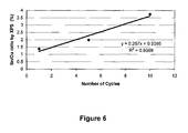
- the method further comprises a step (ab) before (b) of exposing the substrate to a pre-treatment. More preferably, steps (ab) and (b) are repeated until a desired thickness of the adhesion layer is achieved.
- the method further comprises a step (c) of depositing a dielectric barrier layer on the substrate having the adhesion layer. More preferably, the method further comprises a step before (c) of exposing the substrate having the adhesion layer to a post-treatment.
- Yet another embodiment discloses a method for processing a semiconductor device having an improved adhesion comprising the steps of:
- the at least one patterned dielectric layer is selected from the group consisting of silicon dioxide, fluorosilicate glass (FSG), organosilicate glass (OSG), carbon doped oxide (CDO), a porous organosilicate glass having a dielectric constant of less than 3.0, and mixtures thereof;
- the at least one patterned conductive metal layer is selected from the group consisting of copper , copper alloys, and mixtures thereof;
- the pre- treatment and the post- treatment are both H 2 plasma; and
- the organotin precursor is selected from the group consisting of tetramethyltin (Me 4 Sn), dibutyldimethyltin, tributyltin hydride, tetraalkyltin, trialkyltin hydride, dialkyltin dihydride, alkylalkoxytin, tetraalkoxytin, te
- the organotin is selected from the group consisting of tetramethyltin (Me 4 Sn), dibutyldimethyltin, tributyltin hydride, tetraalkyltin, trialkyltin hydride, dialkyltin dihydride, alkylalkoxytin, tetraalkoxytin, tetrakis(dialkylamino)tin, tin hydride (SnH 4 ), tin deuteride (SnD 4 ), and mixtures thereof.
- tetramethyltin Me 4 Sn
- dibutyldimethyltin dibutyldimethyltin
- tributyltin hydride tetraalkyltin
- trialkyltin hydride dialkyltin dihydride
- alkylalkoxytin tetraalkoxytin
- tetrakis(dialkylamino)tin tin
- the at least one patterned dielectric layer preferably comprises a material selected from the group consisting of silicon dioxide, fluorosilicate glass (FSG), organosilicate glass (OSG, aka carbon doped oxide (CDO)), a porous organosilicate glass having a dielectric constant of less than 3.0, and mixtures thereof.
- the at least one patterned conductive metal layer can be a copper, copper alloy layer, or mixtures thereof.
- the organometallic precursor is preferably selected from the group consisting of tetramethyltin (Me 4 Sn), dibutyldimethyltin, tributyltin hydride, tetraalkyltin, trialkyltin hydride, dialkyltin dihydride, alkylalkoxytin, tetraalkoxytin, tetrakis(dialkylamino)tin, tin hydride (SnH 4 ), tin deuteride (SnD 4 ), cyclopentadienyl cobalt dicarbonyl (CpCo(CO) 2 ), nitrosyl cobalt pentacarbonyl, cyclopentadienyl manganese tricarbonyl (CpMn(CO) 3 ), bis(ethylcyclopentadienyl)nickel ((EtCp) 2 Ni), diethylzinc (Et 2 Zn), diethylzinc
- the organotin precursor is preferably selected from the group consisting of tetramethyltin (Me 4 Sn), dibutyldimethyltin, tributyltin hydride, tetraalkyltin, trialkyltin hydride, dialkyltin dihydride, Alkylalkoxytin, tetraalkoxytin, tetrakis(dialkylamino)tin, tin hydride (SnH 4 ), tin deuteride (SnD 4 ), and mixtures thereof.
- tetramethyltin Me 4 Sn
- dibutyldimethyltin dibutyldimethyltin
- tributyltin hydride tetraalkyltin
- trialkyltin hydride dialkyltin dihydride
- Alkylalkoxytin tetraalkoxytin
- tetrakis(dialkylamino)tin
- the dielectric barrier layer is preferably selected from the group consisting of: silicon nitride, silicon oxide, silicon carbide, silicon oxycarbide, silicon oxynitride, silicon carbonitride, silicon oxycarbonitride and mixtures thereof.
- the barrier layer preferably has a dielectric constant of less than 7.
- the pre-treatment and the post-treatment are preferably selected from the group consisting of H 2 plasma, NH 3 plasma, H 2 /He plasma, and H 2 /N 2 plasma.
- the organometallic precursor preferably contains a material selected from the group consisting of zinc, silver, chromium, tin, manganese, nickel, aluminum, and cobalt.
- the deposition process used in the present invention can be any known process such as, Atomic Layer Deposition (ALD), Atomic Layer Treatment (ALT), Plasma Enhanced Atomic Layer Deposition (PEALD), Chemical Vapor Deposition(CVD), and Plasma Enhanced Chemical Vapor Deposition (PECVD), Low Pressure Chemical Vapor Deposition (LPCVD), Sub Atmospheric Chemical Vapor Deposition (SACVD), UV-assisted Chemical Vapor Deposition, Filament -assisted Chemical Vapor Deposition (FACVD), and Atmospheric Pressure Chemical Vapor Deposition (APCVD).
- ALD Atomic Layer Deposition
- ALT Atomic Layer Treatment
- PEALD Plasma Enhanced Atomic Layer Deposition
- CVD Chemical Vapor Deposition
- PECVD Plasma Enhanced Chemical Vapor Deposition
- LPCVD Low Pressure Chemical Vapor Deposition
- SACVD Sub Atmospheric Chemical Vapor Deposition
- FACVD Filament -assisted Chemical Vapor Deposition
- the precursor can be delivered by DLI of either a pure liquid precursor or by DLI of a mixture of the precursor with a solvent in a vessel or a container that is designed for the deposition delivery.
- a typical container comprises an interior volume bounded by interior wall, an inlet, and an outlet.
- Organometallic precursors are vaporized either in the pure form or as mixtures, and the resulting precursor vapor, typically mixed with a carrier gas (such as argon, helium or nitrogen) is transported to a reactor, for example, a chemical vapor deposition (CVD) reactor.
- the organometallic precursor can comprise a solvent which solubilizes the organometallic precursor without decomposing it.
- the weight % of the solvent can be ranging from 5% to 99%; preferably 50% to 90%.
- Suitable solvents can be simple hydrocarbons of the basic formula C n H (2n+2-x) ; where n is 3-10 and x is equal to the number of cyclic structures or the degrees of unsaturation; for example, hexane, hexadiene, pentane, heptane, cyclohexane, cyclooctane or an aromatic hydrocarbon of the general structure C 6 H (6-b) R b where R can be 0-6 and can be the same or different, for example toluene, mesytelene, xylene, para-cymene and combinations thereof.
- the solvent should solubilise the organometallic precursor without decomposing the organometallic precursor.
- organometallic precursors may also be soluble in oxygen containing solvents such as ethers, for example diethyl ether, methyl isobutyl ether, or tetrahydrofuran, alcohols, for example methanol, ethanol, or isopropanol, ketones for example acetone, aldehydes, or esters.
- oxygen containing solvent is selected from the group consisting of an ester, an alcohol and mixtures thereof.
- the structure can further have a metal barrier layer formed between the patterned dielectric layer and the embedded conductive metal features.
- the metal barrier layer preferably comprises materials such as tantalum, tantalum nitride, titanium, titanium nitride, cobalt, ruthenium, and other advanced barrier materials which prevent diffusion of the copper into the dielectric material.
- film treatments were carried out on an Applied Materials Precision-5000 system equipped to process 200 mm silicon wafers. Thermal treatments were carried out in a DxL vacuum chamber, organometallic precursors were delivered to the chamber either by vapor draw or entrained with helium as a carrier gas. Plasma treatments and deposition of silicon nitride films were carried out in a DxL vacuum chamber that was fitted with an Advance Energy 200 rf generator. Adhesive energies were measured via 4-point bend using a DTS Company Delaminator instrument. Bulk film resistivity was measured on 100 nm thick copper films using a 4-point probe.
- Silicon nitride cap layers were deposited using a standard Si 3 N 4 deposition recipe: 100 sccm NH 3 , 75 sccm SiH 4 , 2000 sccm N 2 , 3.5 torr (470 Pa) chamber pressure, 400 mili-inch (1 cm) susceptor to wafer spacing, 300° C wafer temperature, and 300 W power.
- Organometallic precursors evaluated were tetramethyltin (Me 4 Sn), cyclopentadienyl cobalt dicarbonyl (CpCo(CO) 2 ), cyclopentadienyl manganese tricarbonyl (CpMn(CO) 3 ), and bis(ethyl-cyclopentadienyl) nickel ((EtCp) 2 Ni). Adhesion measurements are widely viewed as an acceptable surrogate measurement to predict performance in promoting electromigration resistance. Adhesion values were measured for copper films treated with various processes and capped with 400 nm of PEVCD Si 3 N 4 .
- 4-Point bend measurements were made by gluing a piece of silicon wafer on top of the Si 3 N 4 film with epoxy, notching the top silicon wafer and using standard 4-point bend techniques.
- a 15 nm thick layer of chromium followed by a 150 nm thick layer of aluminum were deposited by sputtering onto both the silicon wafer and the Si 3 N 4 in order to improve the adhesion strength of the epoxy.
- a 400 nm thick layer of Si 3 N 4 was deposited on top of a copper film that had not been treated, these films failed at the Si 3 N 4 / copper interface with a value of 4.0 +/- 0.5 J/m 2 .
- a series of films were exposed to 30 second hydrogen plasma to examine a baseline process for copper film pretreatment.
- a copper film was treated with a 30 second H 2 plasma followed by deposition of 400 nm of PECVD Si 3 N 4 .
- Measurement of the adhesion with the 4-point bend technique revealed an adhesion value of 12.5 J/m 2 .
- To examine the impact of a H 2 plasma on the bulk resistivity of a copper film a 100 nm thick copper film with a bulk resistivity of 0.22 ohm-cm as measured by 4-point probe was exposed to a H 2 plasma for 30 seconds after which time the bulk resistivity was measured as 0.19 ohm-cm. This decrease is presumably due to the reduction of a thin copper oxide layer on top of the copper.
- porous OSG PDEMS films were deposited by flowing a blend of diethoxymethylsilane (DEMS) and alpha terpinene into a vacuum chamber, striking a plasma to co-deposit an organosilicate glass (OSG) and a sacrificial organic porogen. This film is then annealed in using ultraviolet light to remove the sacrificial porogen to yield a porous OSG.
- the porous OSG PDEMS films were then exposed to a 30 second H 2 plasma.
- a series of films were exposed to a 30 second hydrogen plasma pre-treatment, followed by exposure to a mixture of 5% SiH 4 in nitrogen at 4.5 torr (600 Pa) for a variable amount of time, and finally to a NH 3 plasma for 30 seconds post-treatment as shown below, in order to examine a baseline process for copper treatment.
- EXAMPLE 4 Exposure of a copper film to H 2 plasma pre-treatment, Tetramethyltin (Me 4 Sn), without post exposure treatment
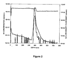
- the porous OSG deposited as described in Example 2 was exposed to an organometallic precursor: 9% mixture of Me 4 Sn in helium at 300° C for 20 seconds, this resulted in a increase in the dielectric constant from 2.2 to 2.3, a minor change in leakage current from ⁇ 8 pico-amperes to 7 pico-amperes, and a minor change in breakdown voltage from ⁇ 4 to 4.18 MV/m.
- the last measurement was also repeated for the exposure to Me 4 Sn after a 30 second H 2 plasma treatment.
- EXAMPLE 6 Exposure of a copper film to H 2 plasma pre-treatment, tetramethyltin (Me 4 Sn) and H 2 plasma post-treatment
- EXAMPLE 7 Exposure of a copper film to H 2 plasma pre-treatment, Cyclopentadienyl Cobalt Dicarbonyl (Cpco(CO) 2 ) and H 2 plasma post-treatment
- EXAMPLE 8 Exposure of a copper film to H 2 plasma pre-treatment, Cyclopentadienyl Manganese Tricarbonyl (CpMn(CO) 3 ) and H 2 plasma post-treatment
- EXAMPLE 9 Exposure of a copper film to H 2 plasma pre-treatment, Bis(ethylcyclopentadienyl)Nickel (EtCp 2 Ni) with H 2 plasma post-treatment
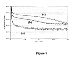
- Table I shows the effect of various processes on the adhesion between the copper layer and the capping PECVD deposited Si 3 N 4 . These measurements were carried out by the industry standard 4-point bend technique. Unless otherwise noted all films were pretreated with a hydrogen plasma. The untreated copper film shows a low adhesion value of 4 +/- 0.5 J/m 2 with delamination at the Si 3 N 4 to copper interface due to the poor adhesion to the native oxide found on copper films. Treatment with hydrogen plasma will reduce the copper oxide back to copper metal and an adhesion value of 12.6 J/m 2 is measured with failure observed between the Si 3 N 4 and the copper interface.
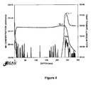
- Table II shows the effect of various copper treatments on the bulk resistivity of a 100nm thick copper film as measured by 4-point probe before and after treatment. All treatments were carried out at 300° C. Exposure of the copper films to just hydrogen or ammonia plasmas lower the bulk resistivity by 8 to 17% presumably due to reduction of the native copper oxide layer found on top of the untreated films. Exposure of the copper to either 5 or 10 seconds of SiH 4 in the "standard silane process" results in significant bulk resistivity increases of 89 and 122% respectively, presumably due to formation of CuSiN and diffusion of Si into the bulk of the copper. Exposure of the copper layer to Me 4 Sn for either 10 or 20 seconds with pre and post hydrogen plasma treatments results in decrease the bulk resistivity by 16 and 13% respectively.
- Table III shows the effect of Me 4 Sn on the electrical performance of porous organosilicate films such as those produced by PDEMS TM ILD deposition process with a dielectric constant of ⁇ 2.2.
- This experiment was performed to determine if the Me 4 Sn would diffuse into the pores of a porous OSG potentially degrading the electrical performance of the porous OSG.
- a PDEMSTM film with a measured dielectric constant of ⁇ 2.2 was exposed to Me 4 Sn for 10 seconds at 300° C.
- the dielectric constant, leakage current and breakdown voltages are either unaffected or only minimally affected by exposure to the Me 4 Sn.
- These measurements were also run after exposure of the PDEMSTM to a hydrogen plasma and the values are given.
- the hydrogen plasma results in a increase in dielectric constant and leakage current. Exposure of the hydrogen plasma treated films to Me 4 Sn for 10 and 20 seconds does not significantly affect the dielectric constant or breakdown voltage. There is a measured difference in leakage current upon exposure to the Me 4 Sn. However, we
- EXAMPLE 11 Exposure of a copper film to H 2 plasma pre-treatment, tetramethyltin / anhydrous hexane mixture with NH3 plasma post-treatment
- a solvent such as hexane which does not influence the tin treatment offers advantages in safety and handling.
Landscapes
- Chemical & Material Sciences (AREA)
- General Chemical & Material Sciences (AREA)
- Chemical Kinetics & Catalysis (AREA)
- Engineering & Computer Science (AREA)
- Materials Engineering (AREA)
- Mechanical Engineering (AREA)
- Metallurgy (AREA)
- Organic Chemistry (AREA)
- Internal Circuitry In Semiconductor Integrated Circuit Devices (AREA)
- Chemical Vapour Deposition (AREA)
- Electrodes Of Semiconductors (AREA)
- Formation Of Insulating Films (AREA)
Applications Claiming Priority (3)
| Application Number | Priority Date | Filing Date | Title |
|---|---|---|---|
| US3887408P | 2008-03-24 | 2008-03-24 | |
| US7484308P | 2008-06-23 | 2008-06-23 | |
| US12/406,467 US8043976B2 (en) | 2008-03-24 | 2009-03-18 | Adhesion to copper and copper electromigration resistance |
Publications (4)
| Publication Number | Publication Date |
|---|---|
| EP2105960A2 true EP2105960A2 (de) | 2009-09-30 |
| EP2105960A3 EP2105960A3 (de) | 2012-04-04 |
| EP2105960B1 EP2105960B1 (de) | 2017-08-02 |
| EP2105960B8 EP2105960B8 (de) | 2017-10-11 |
Family
ID=40793197
Family Applications (1)
| Application Number | Title | Priority Date | Filing Date |
|---|---|---|---|
| EP09155899.9A Active EP2105960B8 (de) | 2008-03-24 | 2009-03-23 | Verbesserte Haftung an Kupfer für verbesserten Kupfer-Elektromigrationswiderstand |
Country Status (6)
| Country | Link |
|---|---|
| US (1) | US8043976B2 (de) |
| EP (1) | EP2105960B8 (de) |
| JP (1) | JP5266116B2 (de) |
| KR (2) | KR101169501B1 (de) |
| CN (1) | CN101609810B (de) |
| TW (1) | TWI479567B (de) |
Cited By (1)
| Publication number | Priority date | Publication date | Assignee | Title |
|---|---|---|---|---|
| WO2012054688A3 (en) * | 2010-10-22 | 2012-06-07 | Applied Materials, Inc. | Methods for enhancing tantalum filament life in hot wire chemical vapor deposition processes |
Families Citing this family (14)
| Publication number | Priority date | Publication date | Assignee | Title |
|---|---|---|---|---|
| JP5530118B2 (ja) * | 2009-04-08 | 2014-06-25 | 東京エレクトロン株式会社 | 酸化マンガン膜の形成方法、半導体装置の製造方法および半導体装置 |
| JP2013213269A (ja) * | 2012-04-04 | 2013-10-17 | Tokyo Electron Ltd | 成膜方法及び記憶媒体 |
| KR101715964B1 (ko) | 2012-06-04 | 2017-03-13 | 삼성에스디아이 주식회사 | 이차 전지 |
| US11761086B2 (en) * | 2014-02-23 | 2023-09-19 | Entegris, Inc. | Cobalt precursors |
| US9673042B2 (en) | 2015-09-01 | 2017-06-06 | Applied Materials, Inc. | Methods and apparatus for in-situ cleaning of copper surfaces and deposition and removal of self-assembled monolayers |
| KR102019468B1 (ko) * | 2016-11-29 | 2019-09-06 | 주식회사 엘지화학 | 반도체용 접착 필름 및 반도체 장치 |
| US11571876B2 (en) | 2017-03-17 | 2023-02-07 | Intel Corporation | Dielectric film with pressure sensitive microcapsules of adhesion promoter |
| CA2975104A1 (en) | 2017-08-02 | 2019-02-02 | Seastar Chemicals Inc. | Organometallic compounds and methods for the deposition of high purity tin oxide |
| US10580645B2 (en) * | 2018-04-30 | 2020-03-03 | Asm Ip Holding B.V. | Plasma enhanced atomic layer deposition (PEALD) of SiN using silicon-hydrohalide precursors |
| JP7213642B2 (ja) * | 2018-09-05 | 2023-01-27 | 東京エレクトロン株式会社 | レジスト膜の製造方法 |
| US11769692B2 (en) | 2018-10-31 | 2023-09-26 | Taiwan Semiconductor Manufacturing Co., Ltd. | High breakdown voltage inter-metal dielectric layer |
| JP2022161040A (ja) * | 2019-09-17 | 2022-10-21 | 株式会社Adeka | 原子層堆積法のための薄膜形成原料及びそれを用いた亜鉛含有薄膜の製造方法 |
| JP7345787B2 (ja) * | 2020-04-30 | 2023-09-19 | 東京エレクトロン株式会社 | 選択成膜方法 |
| US12014956B2 (en) | 2021-09-28 | 2024-06-18 | Applied Materials, Inc. | Tungsten gapfill using molybdenum co-flow |
Citations (5)
| Publication number | Priority date | Publication date | Assignee | Title |
|---|---|---|---|---|
| WO2001008213A1 (en) | 1999-07-27 | 2001-02-01 | International Business Machines Corporation | REDUCED ELECTROMIGRATION AND STRESS INDUCED MIGRATION OF Cu WIRES BY SURFACE COATING |
| US7013916B1 (en) | 1997-11-14 | 2006-03-21 | Air Products And Chemicals, Inc. | Sub-atmospheric gas delivery method and apparatus |
| US7153774B2 (en) | 2002-06-06 | 2006-12-26 | Intel Corporation | Method of making a semiconductor device that has copper damascene interconnects with enhanced electromigration reliability |
| US7193325B2 (en) | 2004-04-30 | 2007-03-20 | Taiwan Semiconductor Manufacturing Company, Ltd. | Reliability improvement of SiOC etch with trimethylsilane gas passivation in Cu damascene interconnects |
| US7229911B2 (en) | 2004-04-19 | 2007-06-12 | Applied Materials, Inc. | Adhesion improvement for low k dielectrics to conductive materials |
Family Cites Families (29)
| Publication number | Priority date | Publication date | Assignee | Title |
|---|---|---|---|---|
| JPH07161034A (ja) * | 1993-04-13 | 1995-06-23 | Matsushita Electric Ind Co Ltd | 磁気記録媒体 |
| US6444264B2 (en) * | 1995-03-31 | 2002-09-03 | Advanced Technology Materials, Inc. | Method for liquid delivery CVD utilizing alkane and polyamine solvent compositions |
| GB9724168D0 (en) * | 1997-11-14 | 1998-01-14 | Air Prod & Chem | Gas control device and method of supplying gas |
| US6147000A (en) * | 1998-08-11 | 2000-11-14 | Advanced Micro Devices, Inc. | Method for forming low dielectric passivation of copper interconnects |
| US6355571B1 (en) * | 1998-11-17 | 2002-03-12 | Applied Materials, Inc. | Method and apparatus for reducing copper oxidation and contamination in a semiconductor device |
| US6479389B1 (en) * | 1999-10-04 | 2002-11-12 | Taiwan Semiconductor Manufacturing Company | Method of doping copper metallization |
| US6984591B1 (en) * | 2000-04-20 | 2006-01-10 | International Business Machines Corporation | Precursor source mixtures |
| US6645550B1 (en) * | 2000-06-22 | 2003-11-11 | Applied Materials, Inc. | Method of treating a substrate |
| US20020048926A1 (en) * | 2000-09-14 | 2002-04-25 | Konecni Anthony J. | Method for forming a self-aligned copper capping diffusion barrier |
| US7351449B2 (en) * | 2000-09-22 | 2008-04-01 | N Gimat Co. | Chemical vapor deposition methods for making powders and coatings, and coatings made using these methods |
| US20020089063A1 (en) * | 2001-01-08 | 2002-07-11 | Ahn Kie Y. | Copper dual damascene interconnect technology |
| US6518167B1 (en) * | 2002-04-16 | 2003-02-11 | Advanced Micro Devices, Inc. | Method of forming a metal or metal nitride interface layer between silicon nitride and copper |
| US6846515B2 (en) * | 2002-04-17 | 2005-01-25 | Air Products And Chemicals, Inc. | Methods for using porogens and/or porogenated precursors to provide porous organosilica glass films with low dielectric constants |
| KR100443796B1 (ko) | 2002-06-29 | 2004-08-11 | 주식회사 하이닉스반도체 | 구리 금속 배선 형성방법 |
| JP3992588B2 (ja) * | 2002-10-23 | 2007-10-17 | 東京エレクトロン株式会社 | 成膜方法 |
| CN100345999C (zh) * | 2003-01-02 | 2007-10-31 | 上海华虹(集团)有限公司 | 采用含钛有机金属材料的化学气相淀积含硅氮化钛的工艺 |
| KR100974778B1 (ko) | 2003-06-30 | 2010-08-06 | 삼성전자주식회사 | 유기금속 전구체 조성물 및 이를 이용한 금속 필름 또는패턴 형성방법 |
| KR100546209B1 (ko) * | 2003-07-09 | 2006-01-24 | 매그나칩 반도체 유한회사 | 반도체 소자의 구리 배선 형성 방법 |
| US6979625B1 (en) * | 2003-11-12 | 2005-12-27 | Advanced Micro Devices, Inc. | Copper interconnects with metal capping layer and selective copper alloys |
| FR2868085B1 (fr) | 2004-03-24 | 2006-07-14 | Alchimer Sa | Procede de revetement selectif d'une surface composite, fabrication d'interconnexions en microelectronique utilisant ce procede, et circuits integres |
| FR2868709B1 (fr) * | 2004-04-08 | 2006-06-23 | Rexam Dispensing Systems Sas | Distributeur sans reprise d'air pour la delivrance de faibles doses de produits liquides et, en particulier, de produits cosmetiques ou pharmaceutiques |
| JP2006063386A (ja) | 2004-08-26 | 2006-03-09 | Tokyo Electron Ltd | 半導体装置の製造方法 |
| US7332445B2 (en) * | 2004-09-28 | 2008-02-19 | Air Products And Chemicals, Inc. | Porous low dielectric constant compositions and methods for making and using same |
| US7476618B2 (en) * | 2004-10-26 | 2009-01-13 | Asm Japan K.K. | Selective formation of metal layers in an integrated circuit |
| US7247946B2 (en) * | 2005-01-18 | 2007-07-24 | International Business Machines Corporation | On-chip Cu interconnection using 1 to 5 nm thick metal cap |
| JP5116251B2 (ja) * | 2005-05-20 | 2013-01-09 | 株式会社半導体エネルギー研究所 | 半導体装置の作製方法 |
| JP2007035734A (ja) * | 2005-07-25 | 2007-02-08 | Nec Electronics Corp | 半導体装置およびその製造方法 |
| TW200802703A (en) * | 2005-11-28 | 2008-01-01 | Nxp Bv | Method of forming a self aligned copper capping layer |
| US20070299239A1 (en) | 2006-06-27 | 2007-12-27 | Air Products And Chemicals, Inc. | Curing Dielectric Films Under A Reducing Atmosphere |
-
2009
- 2009-03-18 US US12/406,467 patent/US8043976B2/en active Active
- 2009-03-20 TW TW098109291A patent/TWI479567B/zh active
- 2009-03-23 EP EP09155899.9A patent/EP2105960B8/de active Active
- 2009-03-24 KR KR1020090025008A patent/KR101169501B1/ko active Active
- 2009-03-24 CN CN200910138735.XA patent/CN101609810B/zh active Active
- 2009-03-24 JP JP2009072147A patent/JP5266116B2/ja not_active Expired - Fee Related
-
2011
- 2011-01-17 KR KR1020110004600A patent/KR20110019398A/ko not_active Ceased
Patent Citations (5)
| Publication number | Priority date | Publication date | Assignee | Title |
|---|---|---|---|---|
| US7013916B1 (en) | 1997-11-14 | 2006-03-21 | Air Products And Chemicals, Inc. | Sub-atmospheric gas delivery method and apparatus |
| WO2001008213A1 (en) | 1999-07-27 | 2001-02-01 | International Business Machines Corporation | REDUCED ELECTROMIGRATION AND STRESS INDUCED MIGRATION OF Cu WIRES BY SURFACE COATING |
| US7153774B2 (en) | 2002-06-06 | 2006-12-26 | Intel Corporation | Method of making a semiconductor device that has copper damascene interconnects with enhanced electromigration reliability |
| US7229911B2 (en) | 2004-04-19 | 2007-06-12 | Applied Materials, Inc. | Adhesion improvement for low k dielectrics to conductive materials |
| US7193325B2 (en) | 2004-04-30 | 2007-03-20 | Taiwan Semiconductor Manufacturing Company, Ltd. | Reliability improvement of SiOC etch with trimethylsilane gas passivation in Cu damascene interconnects |
Cited By (1)
| Publication number | Priority date | Publication date | Assignee | Title |
|---|---|---|---|---|
| WO2012054688A3 (en) * | 2010-10-22 | 2012-06-07 | Applied Materials, Inc. | Methods for enhancing tantalum filament life in hot wire chemical vapor deposition processes |
Also Published As
| Publication number | Publication date |
|---|---|
| EP2105960A3 (de) | 2012-04-04 |
| CN101609810A (zh) | 2009-12-23 |
| KR20090101859A (ko) | 2009-09-29 |
| KR101169501B1 (ko) | 2012-07-27 |
| KR20110019398A (ko) | 2011-02-25 |
| EP2105960B1 (de) | 2017-08-02 |
| JP5266116B2 (ja) | 2013-08-21 |
| US8043976B2 (en) | 2011-10-25 |
| TW200945440A (en) | 2009-11-01 |
| US20090236745A1 (en) | 2009-09-24 |
| CN101609810B (zh) | 2014-06-04 |
| JP2009239283A (ja) | 2009-10-15 |
| EP2105960B8 (de) | 2017-10-11 |
| TWI479567B (zh) | 2015-04-01 |
Similar Documents
| Publication | Publication Date | Title |
|---|---|---|
| EP2105960B1 (de) | Verbesserte Haftung an Kupfer für verbesserten Kupfer-Elektromigrationswiderstand | |
| US6380080B2 (en) | Methods for preparing ruthenium metal films | |
| Au et al. | Selective chemical vapor deposition of manganese self-aligned capping layer for Cu interconnections in microelectronics | |
| US6037001A (en) | Method for the chemical vapor deposition of copper-based films | |
| Vos et al. | Atomic layer deposition of cobalt using H2-, N2-, and NH3-based plasmas: on the role of the co-reactant | |
| EP1354980B1 (de) | Verfahren zur Herstellung einer porösen SiOCH-Schicht | |
| US7799671B1 (en) | Interfacial layers for electromigration resistance improvement in damascene interconnects | |
| US8293001B2 (en) | Porogens, porogenated precursors and methods for using the same to provide porous organosilica glass films with low dielectric constants | |
| US6846515B2 (en) | Methods for using porogens and/or porogenated precursors to provide porous organosilica glass films with low dielectric constants | |
| EP1115900B1 (de) | Herstellungsverfahren für ruthenium-metallschichten | |
| KR100691870B1 (ko) | 동염기성 필름의 화학증착방법 및 그것을 위한 동원전구체 | |
| EP2251899B1 (de) | Abscheidung einer dielektrischen Sperre mittels stickstoffhaltigem Vorläufer | |
| Hong et al. | Atomic layer deposition of Ru thin films using a Ru (0) metallorganic precursor and O2 | |
| Lu et al. | A new process for depositing tungsten nitride thin films | |
| Mao et al. | Scaling of copper seed layer thickness using plasma-enhanced ALD and optimized precursors | |
| Hinz et al. | Analysis of NbN thin film deposition by plasma-enhanced ALD for gate electrode application | |
| US20110081503A1 (en) | Method of depositing stable and adhesive interface between fluorine-based low-k material and metal barrier layer | |
| US20120328798A1 (en) | Inter-low-permittivity layer insulating film, and method for forming inter-low-permittivity layer insulating film | |
| Papadimitropoulos et al. | Copper Films Deposited by Hot‐Wire CVD and Direct Liquid Injection of CupraSelect | |
| Wojcik et al. | A comparative study of thermal and plasma enhanced ALD Ta-NC films on SiO 2, SiCOH and Cu substrates | |
| Martini | Metallization and modification of low-k dielectric materials | |
| Kim et al. | Properties of chemically vapor deposited blanket tungsten films on tin glue layers prepared by chemical vapor deposition | |
| Shimizu et al. | CVD and ALD of Cobalt-tungsten alloy film as a novel Copper diffusion barrier | |
| Gatineau et al. | A New Liquid Precursor for Pure Ruthenium Depositions | |
| Barton | Chemical vapor deposition and atomic layer deposition of metal oxide and nitride thin films |
Legal Events
| Date | Code | Title | Description |
|---|---|---|---|
| PUAI | Public reference made under article 153(3) epc to a published international application that has entered the european phase |
Free format text: ORIGINAL CODE: 0009012 |
|
| AK | Designated contracting states |
Kind code of ref document: A2 Designated state(s): AT BE BG CH CY CZ DE DK EE ES FI FR GB GR HR HU IE IS IT LI LT LU LV MC MK MT NL NO PL PT RO SE SI SK TR |
|
| AX | Request for extension of the european patent |
Extension state: AL BA RS |
|
| RIC1 | Information provided on ipc code assigned before grant |
Ipc: H01L 21/768 20060101AFI20111101BHEP Ipc: C23C 16/18 20060101ALI20111101BHEP |
|
| PUAL | Search report despatched |
Free format text: ORIGINAL CODE: 0009013 |
|
| AK | Designated contracting states |
Kind code of ref document: A3 Designated state(s): AT BE BG CH CY CZ DE DK EE ES FI FR GB GR HR HU IE IS IT LI LT LU LV MC MK MT NL NO PL PT RO SE SI SK TR |
|
| AX | Request for extension of the european patent |
Extension state: AL BA RS |
|
| RIC1 | Information provided on ipc code assigned before grant |
Ipc: H01L 21/768 20060101AFI20120228BHEP Ipc: C23C 16/18 20060101ALI20120228BHEP |
|
| 17P | Request for examination filed |
Effective date: 20121001 |
|
| AKX | Designation fees paid |
Designated state(s): AT BE BG CH CY CZ DE DK EE ES FI FR GB GR HR HU IE IS IT LI LT LU LV MC MK MT NL NO PL PT RO SE SI SK TR |
|
| 17Q | First examination report despatched |
Effective date: 20150611 |
|
| GRAP | Despatch of communication of intention to grant a patent |
Free format text: ORIGINAL CODE: EPIDOSNIGR1 |
|
| RIC1 | Information provided on ipc code assigned before grant |
Ipc: C23C 16/56 20060101ALI20170213BHEP Ipc: C23C 16/18 20060101ALI20170213BHEP Ipc: H01L 21/285 20060101ALI20170213BHEP Ipc: H01L 21/768 20060101AFI20170213BHEP Ipc: C23C 16/02 20060101ALI20170213BHEP |
|
| INTG | Intention to grant announced |
Effective date: 20170301 |
|
| GRAS | Grant fee paid |
Free format text: ORIGINAL CODE: EPIDOSNIGR3 |
|
| GRAA | (expected) grant |
Free format text: ORIGINAL CODE: 0009210 |
|
| AK | Designated contracting states |
Kind code of ref document: B1 Designated state(s): AT BE BG CH CY CZ DE DK EE ES FI FR GB GR HR HU IE IS IT LI LT LU LV MC MK MT NL NO PL PT RO SE SI SK TR |
|
| REG | Reference to a national code |
Ref country code: GB Ref legal event code: FG4D |
|
| GRAM | Information related to correction after decision after decision to grant or to maintain patent in amended form deleted |
Free format text: ORIGINAL CODE: EPIDOSDCDEC |
|
| GRAT | Correction requested after decision to grant or after decision to maintain patent in amended form |
Free format text: ORIGINAL CODE: EPIDOSNCDEC |
|
| REG | Reference to a national code |
Ref country code: CH Ref legal event code: EP Ref country code: AT Ref legal event code: REF Ref document number: 915336 Country of ref document: AT Kind code of ref document: T Effective date: 20170815 |
|
| REG | Reference to a national code |
Ref country code: IE Ref legal event code: FG4D |
|
| REG | Reference to a national code |
Ref country code: DE Ref legal event code: R096 Ref document number: 602009047451 Country of ref document: DE |
|
| RAP2 | Party data changed (patent owner data changed or rights of a patent transferred) |
Owner name: VERSUM MATERIALS US, LLC |
|
| REG | Reference to a national code |
Ref country code: NL Ref legal event code: MP Effective date: 20170802 |
|
| REG | Reference to a national code |
Ref country code: AT Ref legal event code: MK05 Ref document number: 915336 Country of ref document: AT Kind code of ref document: T Effective date: 20170802 |
|
| REG | Reference to a national code |
Ref country code: LT Ref legal event code: MG4D |
|
| PG25 | Lapsed in a contracting state [announced via postgrant information from national office to epo] |
Ref country code: NL Free format text: LAPSE BECAUSE OF FAILURE TO SUBMIT A TRANSLATION OF THE DESCRIPTION OR TO PAY THE FEE WITHIN THE PRESCRIBED TIME-LIMIT Effective date: 20170802 Ref country code: LT Free format text: LAPSE BECAUSE OF FAILURE TO SUBMIT A TRANSLATION OF THE DESCRIPTION OR TO PAY THE FEE WITHIN THE PRESCRIBED TIME-LIMIT Effective date: 20170802 Ref country code: SE Free format text: LAPSE BECAUSE OF FAILURE TO SUBMIT A TRANSLATION OF THE DESCRIPTION OR TO PAY THE FEE WITHIN THE PRESCRIBED TIME-LIMIT Effective date: 20170802 Ref country code: HR Free format text: LAPSE BECAUSE OF FAILURE TO SUBMIT A TRANSLATION OF THE DESCRIPTION OR TO PAY THE FEE WITHIN THE PRESCRIBED TIME-LIMIT Effective date: 20170802 Ref country code: FI Free format text: LAPSE BECAUSE OF FAILURE TO SUBMIT A TRANSLATION OF THE DESCRIPTION OR TO PAY THE FEE WITHIN THE PRESCRIBED TIME-LIMIT Effective date: 20170802 Ref country code: NO Free format text: LAPSE BECAUSE OF FAILURE TO SUBMIT A TRANSLATION OF THE DESCRIPTION OR TO PAY THE FEE WITHIN THE PRESCRIBED TIME-LIMIT Effective date: 20171102 Ref country code: AT Free format text: LAPSE BECAUSE OF FAILURE TO SUBMIT A TRANSLATION OF THE DESCRIPTION OR TO PAY THE FEE WITHIN THE PRESCRIBED TIME-LIMIT Effective date: 20170802 |
|
| REG | Reference to a national code |
Ref country code: FR Ref legal event code: PLFP Year of fee payment: 10 |
|
| PG25 | Lapsed in a contracting state [announced via postgrant information from national office to epo] |
Ref country code: PL Free format text: LAPSE BECAUSE OF FAILURE TO SUBMIT A TRANSLATION OF THE DESCRIPTION OR TO PAY THE FEE WITHIN THE PRESCRIBED TIME-LIMIT Effective date: 20170802 Ref country code: LV Free format text: LAPSE BECAUSE OF FAILURE TO SUBMIT A TRANSLATION OF THE DESCRIPTION OR TO PAY THE FEE WITHIN THE PRESCRIBED TIME-LIMIT Effective date: 20170802 Ref country code: BG Free format text: LAPSE BECAUSE OF FAILURE TO SUBMIT A TRANSLATION OF THE DESCRIPTION OR TO PAY THE FEE WITHIN THE PRESCRIBED TIME-LIMIT Effective date: 20171102 Ref country code: IS Free format text: LAPSE BECAUSE OF FAILURE TO SUBMIT A TRANSLATION OF THE DESCRIPTION OR TO PAY THE FEE WITHIN THE PRESCRIBED TIME-LIMIT Effective date: 20171202 Ref country code: ES Free format text: LAPSE BECAUSE OF FAILURE TO SUBMIT A TRANSLATION OF THE DESCRIPTION OR TO PAY THE FEE WITHIN THE PRESCRIBED TIME-LIMIT Effective date: 20170802 Ref country code: GR Free format text: LAPSE BECAUSE OF FAILURE TO SUBMIT A TRANSLATION OF THE DESCRIPTION OR TO PAY THE FEE WITHIN THE PRESCRIBED TIME-LIMIT Effective date: 20171103 |
|
| PG25 | Lapsed in a contracting state [announced via postgrant information from national office to epo] |
Ref country code: DK Free format text: LAPSE BECAUSE OF FAILURE TO SUBMIT A TRANSLATION OF THE DESCRIPTION OR TO PAY THE FEE WITHIN THE PRESCRIBED TIME-LIMIT Effective date: 20170802 Ref country code: RO Free format text: LAPSE BECAUSE OF FAILURE TO SUBMIT A TRANSLATION OF THE DESCRIPTION OR TO PAY THE FEE WITHIN THE PRESCRIBED TIME-LIMIT Effective date: 20170802 Ref country code: CZ Free format text: LAPSE BECAUSE OF FAILURE TO SUBMIT A TRANSLATION OF THE DESCRIPTION OR TO PAY THE FEE WITHIN THE PRESCRIBED TIME-LIMIT Effective date: 20170802 |
|
| REG | Reference to a national code |
Ref country code: DE Ref legal event code: R097 Ref document number: 602009047451 Country of ref document: DE |
|
| PG25 | Lapsed in a contracting state [announced via postgrant information from national office to epo] |
Ref country code: IT Free format text: LAPSE BECAUSE OF FAILURE TO SUBMIT A TRANSLATION OF THE DESCRIPTION OR TO PAY THE FEE WITHIN THE PRESCRIBED TIME-LIMIT Effective date: 20170802 Ref country code: EE Free format text: LAPSE BECAUSE OF FAILURE TO SUBMIT A TRANSLATION OF THE DESCRIPTION OR TO PAY THE FEE WITHIN THE PRESCRIBED TIME-LIMIT Effective date: 20170802 Ref country code: SK Free format text: LAPSE BECAUSE OF FAILURE TO SUBMIT A TRANSLATION OF THE DESCRIPTION OR TO PAY THE FEE WITHIN THE PRESCRIBED TIME-LIMIT Effective date: 20170802 |
|
| PLBE | No opposition filed within time limit |
Free format text: ORIGINAL CODE: 0009261 |
|
| STAA | Information on the status of an ep patent application or granted ep patent |
Free format text: STATUS: NO OPPOSITION FILED WITHIN TIME LIMIT |
|
| 26N | No opposition filed |
Effective date: 20180503 |
|
| PG25 | Lapsed in a contracting state [announced via postgrant information from national office to epo] |
Ref country code: SI Free format text: LAPSE BECAUSE OF FAILURE TO SUBMIT A TRANSLATION OF THE DESCRIPTION OR TO PAY THE FEE WITHIN THE PRESCRIBED TIME-LIMIT Effective date: 20170802 |
|
| REG | Reference to a national code |
Ref country code: CH Ref legal event code: PL |
|
| GBPC | Gb: european patent ceased through non-payment of renewal fee |
Effective date: 20180323 |
|
| PG25 | Lapsed in a contracting state [announced via postgrant information from national office to epo] |
Ref country code: MC Free format text: LAPSE BECAUSE OF FAILURE TO SUBMIT A TRANSLATION OF THE DESCRIPTION OR TO PAY THE FEE WITHIN THE PRESCRIBED TIME-LIMIT Effective date: 20170802 |
|
| REG | Reference to a national code |
Ref country code: BE Ref legal event code: MM Effective date: 20180331 |
|
| PG25 | Lapsed in a contracting state [announced via postgrant information from national office to epo] |
Ref country code: LU Free format text: LAPSE BECAUSE OF NON-PAYMENT OF DUE FEES Effective date: 20180323 |
|
| PG25 | Lapsed in a contracting state [announced via postgrant information from national office to epo] |
Ref country code: GB Free format text: LAPSE BECAUSE OF NON-PAYMENT OF DUE FEES Effective date: 20180323 Ref country code: LI Free format text: LAPSE BECAUSE OF NON-PAYMENT OF DUE FEES Effective date: 20180331 Ref country code: BE Free format text: LAPSE BECAUSE OF NON-PAYMENT OF DUE FEES Effective date: 20180331 Ref country code: CH Free format text: LAPSE BECAUSE OF NON-PAYMENT OF DUE FEES Effective date: 20180331 |
|
| PG25 | Lapsed in a contracting state [announced via postgrant information from national office to epo] |
Ref country code: MT Free format text: LAPSE BECAUSE OF NON-PAYMENT OF DUE FEES Effective date: 20180323 |
|
| PG25 | Lapsed in a contracting state [announced via postgrant information from national office to epo] |
Ref country code: TR Free format text: LAPSE BECAUSE OF FAILURE TO SUBMIT A TRANSLATION OF THE DESCRIPTION OR TO PAY THE FEE WITHIN THE PRESCRIBED TIME-LIMIT Effective date: 20170802 |
|
| PG25 | Lapsed in a contracting state [announced via postgrant information from national office to epo] |
Ref country code: PT Free format text: LAPSE BECAUSE OF FAILURE TO SUBMIT A TRANSLATION OF THE DESCRIPTION OR TO PAY THE FEE WITHIN THE PRESCRIBED TIME-LIMIT Effective date: 20170802 Ref country code: HU Free format text: LAPSE BECAUSE OF FAILURE TO SUBMIT A TRANSLATION OF THE DESCRIPTION OR TO PAY THE FEE WITHIN THE PRESCRIBED TIME-LIMIT; INVALID AB INITIO Effective date: 20090323 |
|
| PG25 | Lapsed in a contracting state [announced via postgrant information from national office to epo] |
Ref country code: CY Free format text: LAPSE BECAUSE OF FAILURE TO SUBMIT A TRANSLATION OF THE DESCRIPTION OR TO PAY THE FEE WITHIN THE PRESCRIBED TIME-LIMIT Effective date: 20170802 Ref country code: MK Free format text: LAPSE BECAUSE OF NON-PAYMENT OF DUE FEES Effective date: 20170802 |
|
| PGFP | Annual fee paid to national office [announced via postgrant information from national office to epo] |
Ref country code: FR Payment date: 20210210 Year of fee payment: 13 |
|
| PGFP | Annual fee paid to national office [announced via postgrant information from national office to epo] |
Ref country code: DE Payment date: 20210310 Year of fee payment: 13 |
|
| REG | Reference to a national code |
Ref country code: DE Ref legal event code: R119 Ref document number: 602009047451 Country of ref document: DE |
|
| PG25 | Lapsed in a contracting state [announced via postgrant information from national office to epo] |
Ref country code: FR Free format text: LAPSE BECAUSE OF NON-PAYMENT OF DUE FEES Effective date: 20220331 Ref country code: DE Free format text: LAPSE BECAUSE OF NON-PAYMENT OF DUE FEES Effective date: 20221001 |
|
| P01 | Opt-out of the competence of the unified patent court (upc) registered |
Effective date: 20230602 |
|
| PGFP | Annual fee paid to national office [announced via postgrant information from national office to epo] |
Ref country code: IE Payment date: 20241231 Year of fee payment: 17 |