EP2104797B1 - Light source - Google Patents
Light source Download PDFInfo
- Publication number
- EP2104797B1 EP2104797B1 EP08703413.8A EP08703413A EP2104797B1 EP 2104797 B1 EP2104797 B1 EP 2104797B1 EP 08703413 A EP08703413 A EP 08703413A EP 2104797 B1 EP2104797 B1 EP 2104797B1
- Authority
- EP
- European Patent Office
- Prior art keywords
- sealing member
- substrate
- projections
- light source
- light emitting
- Prior art date
- Legal status (The legal status is an assumption and is not a legal conclusion. Google has not performed a legal analysis and makes no representation as to the accuracy of the status listed.)
- Not-in-force
Links
Images


Classifications
-
- F—MECHANICAL ENGINEERING; LIGHTING; HEATING; WEAPONS; BLASTING
- F21—LIGHTING
- F21K—NON-ELECTRIC LIGHT SOURCES USING LUMINESCENCE; LIGHT SOURCES USING ELECTROCHEMILUMINESCENCE; LIGHT SOURCES USING CHARGES OF COMBUSTIBLE MATERIAL; LIGHT SOURCES USING SEMICONDUCTOR DEVICES AS LIGHT-GENERATING ELEMENTS; LIGHT SOURCES NOT OTHERWISE PROVIDED FOR
- F21K9/00—Light sources using semiconductor devices as light-generating elements, e.g. using light-emitting diodes [LED] or lasers
-
- H—ELECTRICITY
- H01—ELECTRIC ELEMENTS
- H01L—SEMICONDUCTOR DEVICES NOT COVERED BY CLASS H10
- H01L25/00—Assemblies consisting of a plurality of semiconductor or other solid state devices
- H01L25/03—Assemblies consisting of a plurality of semiconductor or other solid state devices all the devices being of a type provided for in a single subclass of subclasses H10B, H10D, H10F, H10H, H10K or H10N, e.g. assemblies of rectifier diodes
- H01L25/04—Assemblies consisting of a plurality of semiconductor or other solid state devices all the devices being of a type provided for in a single subclass of subclasses H10B, H10D, H10F, H10H, H10K or H10N, e.g. assemblies of rectifier diodes the devices not having separate containers
- H01L25/075—Assemblies consisting of a plurality of semiconductor or other solid state devices all the devices being of a type provided for in a single subclass of subclasses H10B, H10D, H10F, H10H, H10K or H10N, e.g. assemblies of rectifier diodes the devices not having separate containers the devices being of a type provided for in group H10H20/00
- H01L25/0753—Assemblies consisting of a plurality of semiconductor or other solid state devices all the devices being of a type provided for in a single subclass of subclasses H10B, H10D, H10F, H10H, H10K or H10N, e.g. assemblies of rectifier diodes the devices not having separate containers the devices being of a type provided for in group H10H20/00 the devices being arranged next to each other
-
- H—ELECTRICITY
- H10—SEMICONDUCTOR DEVICES; ELECTRIC SOLID-STATE DEVICES NOT OTHERWISE PROVIDED FOR
- H10H—INORGANIC LIGHT-EMITTING SEMICONDUCTOR DEVICES HAVING POTENTIAL BARRIERS
- H10H20/00—Individual inorganic light-emitting semiconductor devices having potential barriers, e.g. light-emitting diodes [LED]
- H10H20/80—Constructional details
- H10H20/85—Packages
- H10H20/851—Wavelength conversion means
-
- H—ELECTRICITY
- H10—SEMICONDUCTOR DEVICES; ELECTRIC SOLID-STATE DEVICES NOT OTHERWISE PROVIDED FOR
- H10H—INORGANIC LIGHT-EMITTING SEMICONDUCTOR DEVICES HAVING POTENTIAL BARRIERS
- H10H20/00—Individual inorganic light-emitting semiconductor devices having potential barriers, e.g. light-emitting diodes [LED]
- H10H20/80—Constructional details
- H10H20/85—Packages
- H10H20/855—Optical field-shaping means, e.g. lenses
- H10H20/856—Reflecting means
-
- H—ELECTRICITY
- H10—SEMICONDUCTOR DEVICES; ELECTRIC SOLID-STATE DEVICES NOT OTHERWISE PROVIDED FOR
- H10H—INORGANIC LIGHT-EMITTING SEMICONDUCTOR DEVICES HAVING POTENTIAL BARRIERS
- H10H20/00—Individual inorganic light-emitting semiconductor devices having potential barriers, e.g. light-emitting diodes [LED]
- H10H20/80—Constructional details
- H10H20/85—Packages
- H10H20/858—Means for heat extraction or cooling
- H10H20/8582—Means for heat extraction or cooling characterised by their shape
-
- H—ELECTRICITY
- H10—SEMICONDUCTOR DEVICES; ELECTRIC SOLID-STATE DEVICES NOT OTHERWISE PROVIDED FOR
- H10H—INORGANIC LIGHT-EMITTING SEMICONDUCTOR DEVICES HAVING POTENTIAL BARRIERS
- H10H20/00—Individual inorganic light-emitting semiconductor devices having potential barriers, e.g. light-emitting diodes [LED]
- H10H20/80—Constructional details
- H10H20/85—Packages
- H10H20/858—Means for heat extraction or cooling
- H10H20/8583—Means for heat extraction or cooling not being in contact with the bodies
-
- H—ELECTRICITY
- H01—ELECTRIC ELEMENTS
- H01L—SEMICONDUCTOR DEVICES NOT COVERED BY CLASS H10
- H01L2924/00—Indexing scheme for arrangements or methods for connecting or disconnecting semiconductor or solid-state bodies as covered by H01L24/00
- H01L2924/0001—Technical content checked by a classifier
- H01L2924/0002—Not covered by any one of groups H01L24/00, H01L24/00 and H01L2224/00
Definitions
- the present invention relates to a light source in which semiconductor light emitting elements implemented on the substrate are covered and sealed with a sealing member.
- LED elements which are one example of semiconductor light emitting elements for use therein.
- Each of such light sources includes a substrate, LED elements implemented on a main surface of the substrate, andatranslucent sealingmember formed on the substrate to cover and seal the LED elements.
- the sealing member is often made of resin that contains a phosphor that converts light emitted from the LED elements into light of a desired colour. See EP-A-1 681 728 , US 2006/255352 and WO 2004/099342 and US 2005/0248259 .
- the phosphor accumulates heat that is generated as the thermal energy when the phosphor converts light emitted from the LED elements into light of a desired color.
- the heat increases the temperature of the sealing member, and increases the temperature of the LED elements covered and sealed with the sealing member.
- the light source of this structure has a problem that the light emitting efficiency of the LED elements is decreased by the temperature rise.
- the object of the present invention is therefore to provide a light source that accelerates the release of heat from the sealing member.
- a light source comprising: a substrate, semiconductor light emitting elements that have been implemented on a main surface of the substrate, a sealing member translucent to the light emitted by the semiconductor light emitting elements, wherein the sealing member includes a phosphor and is provided on the main surface of the substrate to cover and seal the semiconductor light emitting elements ; and heat conductors that are provided on the main surface of the substrate as projections from the substrate in an area where the sealing member is provided, such that the heat conductors connect the sealing member with the substrate to conduct heat from the sealing member to the substrate.
- the sealing member may include the phosphor and an organic material.
- the heat conductors may be tapered.
- an outer surface of each of the heat conductors may be a light reflection surface.
- the sealing member has the heat conductor therein.
- the heat accumulated in the phosphor is conducted to the heat conductor, and then conducted to the substrate. This makes it possible to accelerate the release of heat from the sealing member, restricting the temperature rise in the sealing member and the semiconductor light emitting elements. This prevents the light emitting efficiency of the semiconductor light emitting elements from decreasing.
- the following describes a light source as an embodiment of the present invention, in which LED elements are used as semiconductor light emitting elements.
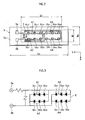
- Fig. 1 is a perspective view of the light source in the present embodiment, which is partially cut away to show the inside.
- a light source 1 includes a substrate 5, a plurality of LED elements Dnm, a sealing member 7, and a plurality of projections (heat conductive members) 11.
- the substrate 5 includes a wiring pattern 3 formed on a main surface 5a.
- the plurality of LED elements Dnm are implemented on the main surface 5a of the substrate 5.
- the sealingmember 7 is attached to the main surface 5a to cover and seal the plurality of LED elements Dnm.
- the plurality of projections 11 are formed on the main surface 5a of the substrate 5.
- Fig. 2 is a plan view of the light source without the sealing member.
- Fig. 3 is a circuit diagram of the light source.
- the light source 1 of the present embodiment includes 12 pieces of LED element Dnm.
- the LED element Dnm is electrically connected to the wiring pattern 3 which is composed of two power supply terminals, namely, power supply terminals 3a and 3b.
- the power supply terminal 3a is, for example, a terminal on the positive electrode side
- the power supply terminal 3b is, for example, a terminal on the negative electrode side.
- Each of the 12 pieces of LED element Dnm is connected such that four series groups An are connected in parallel with each other, where "n” is a natural number of 1 to 4.
- each series group An three LED elements are connected in series. Accordingly, "n” in Dnm identifies one of the series groups, and “m” in Dnm represents one of the three LED elements in a series group, starting from the LED element nearest to the power supply terminal 3b on the negative electrode side.
- the LED elements constituting the second series group A2 are identified as "D21", “D22", and "D23".
- each LED element is merely represented as "Dnm".
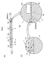
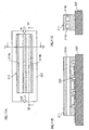
- the part (a) of Fig. 4 is a cross sectional view of the light source.
- the part (b) of Fig. 4 is an expansion of the portion A shown in the part (a) of Fig. 4 .
- the part (c) of Fig. 4 is an expansion of the portion B shown in the part (b) of Fig. 4 .
- each LED element Dnm is implemented on the substrate 5 and covered by the sealing member 7.
- each LED element Dnm is hermetically sealed by the sealing member such that the LED element Dnm is neither exposed to nor in communication with an external air surrounding the sealing member 7.
- LED element Dnm the implementation of the LED element Dnm will be described, using, as an example, an LED element D42 that is shown in the part (b) of Fig. 4 . It should be noted here that the other LED elements Dnm are implemented in the same manner as the LED element D42.
- the LED element D42 is a single surface electrode type in which both the P-type electrode and the N-type electrode are provided on the back surface. These electrodes are connected to and implemented onto the wiring pattern 3 by, for example, bumps 9a and 9b. It should be noted here that the LED element D42 is also connected to the main surface 5a of the substrate 5 by part of the bumps 9a and 9b that has run off the edge of the wiring pattern 3.
- a plurality of projections 11 are formed of the main surface 5a of the substrate 5 in areas in which no LED element Dnm is formed.
- the projections 11 project in a direction perpendicular to the main surface 5a. In other words, the projections 11 project in the vertical direction.
- the sealing member 7 is formed as a mixture of an organic material, such as resin material 7a, and a phosphor 13.
- the phosphor 13 converts the light emitted from the LED elements Dnm into light of a desired color. Here, thermal energy is generated by the conversion of color to cause heat, and the phosphor 13 holds the generated heat. The heat is conveyed to the projections 11 in the vicinity of the phosphor 13, and then to the substrate 5.
- the light source 1 is attached to a lighting instrument that, for example, includes a heat sink (and then the substrate 5 is in close contact with the heat sink), the heat is conveyed from the substrate 5 to the heat sink. This results in the release of the heat having been held by the phosphor 13.
- the light source may have a structure where the LED elements are implemented on one surface of the substrate, and a heat sink is provided on an opposite surface of the substrate.
- the substrate 5 is made of ceramic such as alumina, and has 37 [mm] of length Ls, 12 [mm] of width Bs, and 0.8 [mm] of thickness Ts (see Fig. 2 and the part (a) of Fig. 4 ).
- the wiring pattern 3 is formed on the main surface 5a of the substrate 5 to have a predetermined pattern by applying a sheet of copper foil with 10[ ⁇ m] of thickness thereto by the etching method.
- Each LED element Dnm is substantially in a shape of a rectangular parallelepiped, with its bottom being in a shape of a square of 0.8[mm] ⁇ 0.8[mm], with its height being 0.31[mm].
- Each LED element Dnm is made of InGaN-based material. The color of the light emitted from the LED element Dnm is blue.
- used as the resin material 7a of the sealing member 7 is, for example, silicon resin. Also, used as the material of the phosphor 13 is, for example, a phosphor that emits yellow'light. With this arrangement, the blue light emitted from the LED element Dnm is converted in color by the phosphor 13, and yellow light is emitted from the light source 1.
- the sealing member 7 covers and seals all of the 12 pieces of LED element Dnm, the plurality of projections 11, and the wiring pattern 3, except for the power supply terminals 3a and 3b.
- the sealing member 7 has 26 [mm] of length Lr, 8 [mm] of width Br, and 1.5 [mm] of thickness Tr (see Fig. 2 and the part (a) of Fig. 4 ).
- the phosphor in the sealing member has the following density: 8[wt%] to 10[wt%] (more preferably 9.1 [wt%]) for neutral white light; and 10.5 [wt%] to 12 [wt%] (more preferably 11. 2 [wt%]) for warm white light.
- the reason that these values are preferable is that they can reduce the change over time for each of desired color temperature.
- the plurality of LED elements Dnm are arranged in two rows and six columns in appearance.
- the distance between two adjacent columns is represented as P1 and is approximately 3.8 [mm] (re'fer to the part (a) of Fig. 4 ), and the distance between two adjacent rows is represented as P2 and is approximately 3.8 [mm], where each of these distances is a distance between respective centers of the adjacent LED elements Dnm.
- the part (a) illustrates the arrangement of the projections
- the part (b) is an expansion of a portion of the part (a) of Fig. 5
- the part (c) is a side view of the projection.
- the projections 11 are formed in the entire area of the main surface 5a, except for areas R1 which are each an area surrounding an LED element Dnm.
- the area in which the projections 11 are formed is represented as R2.
- Each area R1 is substantially in a shape of square, where the distance between a side of an LED element Dnm and a side of the surrounding area R1 that is opposite to the side of the LED element Dnm, in a plan view, is 0.5 [mm], and L1 and L2, which represent lengths of sides of each area R1 in different directions are each 1.8[mm].
- the reason that each area R1 is formed in a shape of square is to diffuse the heat uniformly.
- the projections 11 are formed in the area R2 such that each side of a square of 0.1 [mm] ⁇ 0.1[mm] in the area R2 has five projections 11, with respective centers of the projections being on each side of the square in a plan view.
- the formation density of the projections 11 can be defined as 17 pieces of projections per 0.01[mm 2 ].
- each of the projections 11 is cylindrical and has 10 [ ⁇ m] of diameter D1, which is a diameter of the bottom (the circle in the cross section), and has 20[ ⁇ m] of height H1.
- the projections 11 are made of, for example, gold (Au).
- the projections 11 are formed by applying the technology of forming bumps by the ink jet method.
- the heat conductivity of the projections 11 is 290[W/m ⁇ K]
- the heat conductivity of the sealing member 7 is 0.83[W/m ⁇ K] to 4[W/m ⁇ K].
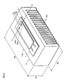
- the temperature of the light source was measured when the light source was laid on a heat sink (15) and all the LED elements Dnm were lighted.
- Fig. 6 illustrates the structure when the temperature was measured.
- a heat sink 15 is substantially in a shape of a rectangular parallelepiped, which is 50 [mm] in length (Lh), 25 [mm] in width (Bh), 15 [mm] in thickness (Th), and 54 [cm 3 ] in volume.
- the heat sink 15 is made of an aluminum material such as an aluminum material plated with white/black alumite.
- the heat sink 15 includes fins 15b for releasing heat on a side thereof that is opposite to a placement surface 15a thereof on which the light source 1 is laid.
- While the light source 1 is laid on substantially the center of the placement surface 15a of the heat sink 15, 800 [mA] of current in total is applied such that 200 [mA] of current flows in each series group An.
- the application voltage for applying the current is 10.5[V].
- the temperature was measured at four locations on a line Z-Z connecting the centers of two LED elements (in this example, D33 and D43) that are adjacent in the column direction (in the X direction in Fig. 2 ).
- the four measurement locations are: L1 that is located on the heat sink 15 and is outside the light source 1; L2 that is located on the substrate 5 and is outside the sealing member 7; L3 that is located on the sealing member 7 and is outside a portion on which the LED element D43 is implemented; and L4 that is located on the LED element D43.
- the temperature was measured at the measurement locations L1 to L4 using a contactless thermometer, and the measurement was performed after a lapse of 30 seconds after all the LED elements Dnm started to be lighted.
- invention example an example of the light source 1 (hereinafter referred to as "invention example") that has the structure of the present invention as described in the embodiment above; an example (hereinafter referred to as “comparative example 1”) that has the structure of the light source 1 except that the sealing member is made of merely resin (not containing a phosphor) and that the projections have not been made; and an example (hereinafter referred to as “comparative example 2”) that has the structure of the light source 1 except that the projections have not been made.
- Fig. 7A shows the temperature measurement results with regard to the invention example and the comparative examples.
- Fig. 7B is a graph of the temperature measurement results.
- the comparative example 2 contains the phosphor 13 within the sealing member 7, and thus the phosphor 13 holds heat when it converts light received from the LED elements Dnm into light of a desired color (thermal energy is generated by the conversion of color, and the heat of the thermal energy remains in the sealing member), while the comparative example 1 does not contain the phosphor that performs the conversion, and thus the thermal energy is not generated by the conversion of color.
- the comparative example 1 does not contain the phosphor, while the invention example includes the sealing member 7 that contains the phosphor 13. It is derived from this that the projections 11 formed on the substrate 5 released the remaining heat from the sealing member 7 completely in substance, so that the invention example with the phosphor and the comparative example 1 without the phosphor had substantially the same temperature distribution.
- the light emitting efficiency of the comparative example 2 was approximately 39 [lm/W], while the light emitting efficiency of the invention example having the projections 11 was approximately 47[lm/W], indicating that the invention example has been improved from the comparative example 2 by approximately 20[%] in the light emitting efficiency.
- the projections 11 in the present embodiment are formed in the shape of a cylinder by applying the technology of forming bumps by the ink jet method. However, not limited to this, the projections may be formed in other shapes.
- the projections 11 may be formed in the shape of a quadrangular prism. Also, the projections 11 may be formed in the shape of a triangular prism, a pentagonal prism, or a prism having six or more angles. Further, the projections may be formed in the shape of a column whose cross-sectional surface'has an ellipsoidal shape.
- the projections 11 may be formed in the shape of a cone whose head has been cut off. Also, the projections 11 may be formed in the shape of a pyramid whose head has been cut off, where a cross-sectional surface of the pyramid has a shape of a quadrangle, triangle, or pentagon, or has six or more angles. Still further, the projections 11 may be formed in the shape of an elliptical cone whose head has been cut off, where a cross-sectional surface of the elliptical cone has an ellipsoidal shape. Still further, the projections 11 maybe formed in a variety of shapes, on the substrate.
- the projections 11 in the present embodiment have the shape of a cylinder, and have 10[ ⁇ m] of diameter D1, which is a diameter of the circle, the shape of a cross-sectional surface, and has 20[ ⁇ m] of height H1 (see the part (c) of Fig. 5 ).
- the size of the projections 11 is not limited to this. However, it is preferable that the cross-sectional surface of the projections 11 is, in size, inside a square whose one side is 5 [ ⁇ m] to 10 [ ⁇ m] long, and that the projections 11 are, in height, in a range from 5[ ⁇ m] to 20[ ⁇ m]. The reason that these ranges are preferable is that the projections 11 in these ranges can be formed easily by the ink jet method.
- the top surface is, in size, inside a square whose one side is 5[ ⁇ m] long. This is because it provides an excellent formability.
- the projections 11 may be formed in a variety of sizes, on the substrate.
- the projections 11 are formed uniformly in substance on the substrate 5, and more specifically, 17 pieces of projections per 0.01 [mm 2 ] are formed.
- the number of projections per unit area is determined appropriately depending on their size and/or the density of the LED elements Dnm. It is preferable that the number of projections per 0.01[mm 2 ] is 100 or less.
- the projections can be formed such that the projections do no interfere with each other, and such that a broad surface area can be ensured with respect to the projections as a whole.
- the projections are arranged uniformly.
- the protections may be arranged nonuniformly as a whole such that the projections are concentrated in a certain area.
- the projections 11 are arranged such that they surround each LED element Dnm completely. However, there is no need for the projections to surround each LED element Dnm completely, but they need to be arranged around each LED element.
- the projections may be arranged such that they surround each set of a plurality of adj acent LED elements (for example, two adjacent LED elements) completely. It is needless to say that the heat releasability is higher when the projections are arranged to surround each LED element Dnm completely, than the other projection arrangement methods.
- the projections 11 are formed by the ink jet method.
- the projections 11 may be formed using a technology of forming stud bumps.
- Fig. 8 shows a projection in which the stud bump is used.
- a projection 101 is a typical stud bump. It is desirable that the stud bump has the following measurements that are determined from the forming technology: diameter D2 in the cross sectional shape is in a range from 60 [ ⁇ m] to 100 [ ⁇ m], for example, 80 [ ⁇ m] and height H2 is in a range from 50[ ⁇ m] to 80[ ⁇ m], for example, 65[ ⁇ m].
- the above-described measurements are desirable for the following reasons. That is to say, when it is taken into consideration that a ball whose diameter is three times that of a wire (for example, for a wire having 18[ ⁇ m] of diameter, the ball should have approximately 60[ ⁇ m] of diameter) is formed first, and the ball is transformed into the shape of a stud bump having a diameter larger than that of the ball, it is considered easy to form stud bumps having the above-described measurements.
- the projections 101 it is further desirable that, in terms of the density of the projections 101, approximately 100 pieces or less of projections 101 are arranged per 1[mm 2 ]. The reason is that the projections can be arranged not to interfere with each other, and that a broad surface area can be ensured with respect to the projections as a whole.
- LED elements are used as the semiconductor light emitting elements.
- other semiconductor light emitting elements such as semiconductor laser, may be used instead.
- the arrangement and number of the semiconductor light emitting elements, the distance between adjacent semiconductor light emitting elements ("P1", "P2" shown in the part (a) of Fig. 5 ), and the like are not limited to those specified in the embodiment.
- the projections as heat conductors are explained with respect to their shape, size, and formation method. Not limited to these, heat conductors of two shapes, for example cylinder and cone, may be used in combination.
- the heat conductor may be made of gold (Au), silver (Ag), copper (Cu), or the like, and may be formed to be tapered such that the outer surface of the heat conductor has a function of a light reflection surface that reflects light, which may be light from the semiconductor light emitting element or may be light from the phosphor after the conversion therein, toward the outside of the sealing member.
- a plurality of heat conductors each having a shape of a projection, are used.
- a plurality of heat conductors may be formed in a shape of a block, bar, plate or the like, to project from the substrate to be present between the semiconductor light emitting elements implemented on the substrate.
- Figs. 9A and 9B show modifications of the heat conductor.
- Fig. 9A shows a heat conductor 101 which is in the shape of a flat plate as a whole, and has holes 103 and 105 each of which corresponds in position to a series of semiconductor light emitting elements Dnm when the heat conductor 101 is attached to the substrate 107.
- the hole 103 contains semiconductor light emitting elements D11 through D16
- the hole 105 contains semiconductor light emitting elements D21 through D26.
- the semiconductor light emitting elements and the heat conductors are covered and sealed by a sealing member 109 that contains the phosphor.
- Fig. 9A only shows semiconductor.light emitting elements D11 through D13 and D21 through D23 in this cut away view, and the remaining semiconductor light emitting elements D14 through D16 and D24 through D26 exist in the sealing member 109.
- Fig. 9B shows a heat conductor 111 that surrounds each' semiconductor light emitting element Dnm.
- the heat conductor 111 is in the shape of a flat plate as a whole, and has holes Knm each of which, when the heat conductor 111 is attached to a substrate 115, corresponds in position to a emiconductor light emitting element Dnm ("n" and “m” are natural numbers, and "n” and “m” in both holes Knm and semiconductor light emitting elements Dnm correspond to each other in terms of their positions).
- a sealing member 113 that contains the phosphor.
- Fig. 9B only shows semiconductor light emitting elements D14 through D16 and D24 through D26 in this cut away view, and the remaining semiconductor light emitting elements D11 through D13 and D21 through D23 are not shown for the sake of convenience.
- the heat conductors shown in Figs. 9A and 9B are single flat plates, respectively. However, not limited to this: a plurality of flat-plates each of which has a plurality of holes at certain positions may be used; or a plurality of flat plates each of which has a hole may be used.
- each hole may be formed such that the opening of the hole (the area of a cross sectional plane of the hole) becomes wider as the opening is distanced away from the substrate, and such that the hole is surrounded by a reflection surface or a reflection film.
- the height of the heat conductor from the substrate is substantially the same as the height of the semiconductor light emitting element.
- the height of the heat conductor from the substrate may be larger or smaller than the height of the semiconductor light emitting element.
- the above-described embodiment adopts a method in which LED elements, as the semiconductor light emitting elements, are directly implemented onto the substrate. Not limited to this, however, it is possible to adopt another method where what is called a submount, in which the semiconductor light emitting elements have been implemented onto a sub-substrate, is implemented onto the (main) substrate.
- specification of the semiconductor light emitting elements is not provided.
- the present invention is not limited by the specification of the semiconductor light emitting elements.
- the present invention is not limited to any colors of light emitted by the light emitting elements.
- semiconductor light emitting elements emitting red light may be used.
- semiconductor light emitting elements emitting blue light may be used and the semiconductor light emitting elements may be covered and sealed with a resin (sealingmember) that contains a phosphor that converts the blue light emitted from the semiconductor light emitting elements into another color of light.
- elements other than LED elements such as laser diode elements, may be used as the semiconductor light emitting elements.
- the alternative element needs not be limited to a specific color of light, a specific size or the like.
- silicon resin is used as the sealing member.
- other resins such as epoxy resin, may be used.
- inorganic materials such as glass (low melting point glass) may be used.
- the sealing member is made of a material that has translucency for transmitting the light emitted from the semiconductor light emitting elements.
- the sealing member may have a mechanism inside for releasing the heat generated by the semiconductor light emitting elements.
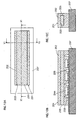
- Figs. 10A through 12C show modifications of the sealing member.
- Fig. 10A is a cross sectional view of the first modification to the sealingmember cut by a plane that is parallel to the substrate.
- Fig. 10B is a cross sectional view taken along a line X1-X1 of Fig. 10A and viewed from a direction as indicated by the arrows nearby.
- Fig. 10C is a cross sectional view taken along a line Y1-Y1 of Fig. 10A and viewed from a direction as indicated by the arrows nearby.
- Fig. 11A is a cross sectional view of the second modification to the sealingmember cut by a plane that is parallel to the substrate.
- Fig. 11B is a cross sectional view taken along a line X2-X2 of Fig. 11A and viewed from a direction as indicated by the arrows nearby.
- Fig. 11C is a cross sectional view taken along a line Y2-Y2 of Fig. 11A and viewed from a direction as indicated by the arrows nearby.
- Fig. 12A is a cross sectional view of the third modification to the sealing member cut by a plane that is parallel to the substrate.
- Fig. 12B is a cross sectional view taken along a line X3-X3 of Fig. 12A and viewed from a direction as indicated by the arrows.
- Fig. 12C is a cross sectional view taken along a line Y3-Y3 of Fig. 12A and viewed from a direction as indicated by the arrows.
- a sealing member 201 shown in Figs. 10A through 10C is in the shape of a rectangular parallelepiped.
- the sealing member 201 is composed of a sealing member body 202 and a filling 205.
- the sealing member body 202 has at least one through hole 203 that passes through from one surface of the sealing member 201 to other opposite surface thereof.
- the filling 205 fills the through hole 203.
- the filling 205 is made of a material that is translucent and has an excellent heat conductivity, such as ceramic or glass.
- the cross sectional shape of the through hole 203 is not limited to a rectangle, but may be in any other shapes such as an ellipse (including a circle), a square, and a polygon. It should be noted here that the sealing member is formed on a substrate 207 on which the semiconductor light emitting elements Dnm have been implemented and heat conductors 209 have been attached.
- a sealing member 211 shown in Figs. 11A through 11C is in the shape of a rectangular parallelepiped.
- the sealing member 211 has one or more through holes (in this example, two through holes 213a and 213b) that pass through from one surface of the sealing member 211 to other opposite surface thereof.
- a fluid forexample, water, air, ornitrogen (including liquid nitrogen)
- a pump for sending out the fluid and pipes for circulating the fluid.
- the cross sectional shape of the through holes is not limited to a rectangle, but may be in any other shapes such as an ellipse (including a circle), a square, and a polygon.
- the through holes need not be formed in the shape of straight pipes, but may be formed in the shape of, for example, bended pipes.
- Asealingmember221 shown in Figs. 12A through 12C is composed of a sealing member body 223 and a cover 225.
- the sealing member body 223 contains a phosphor.
- the cover 225 covers an outer surface of the sealing member body 223 so that the outer surface is not exposed to the air.
- the cover 225 is made of a material that is translucent and has an excellent heat conductivity, such as ceramic or glass. With this structure, the heat accumulated in the phosphor can be released outside through the cover 225.
- the sealing member may be any combination of the above-described embodiment and modifications.
- the substrate is an alumina substrate.
- the substrate may be made of ceramic other than alumina, resin (for example, silicon resin), a material containing glass and epoxy resin, a composite of resin and inorganic filler, metal, or the like.
- the present invention can be used as, for example, a light source for a lighting instrument.
Landscapes
- Engineering & Computer Science (AREA)
- Microelectronics & Electronic Packaging (AREA)
- Physics & Mathematics (AREA)
- Optics & Photonics (AREA)
- General Engineering & Computer Science (AREA)
- Power Engineering (AREA)
- Condensed Matter Physics & Semiconductors (AREA)
- General Physics & Mathematics (AREA)
- Computer Hardware Design (AREA)
- Led Device Packages (AREA)
Applications Claiming Priority (2)
| Application Number | Priority Date | Filing Date | Title |
|---|---|---|---|
| JP2007003881 | 2007-01-11 | ||
| PCT/JP2008/050559 WO2008084878A1 (en) | 2007-01-11 | 2008-01-10 | Light source |
Publications (2)
| Publication Number | Publication Date |
|---|---|
| EP2104797A1 EP2104797A1 (en) | 2009-09-30 |
| EP2104797B1 true EP2104797B1 (en) | 2013-07-31 |
Family
ID=39387265
Family Applications (1)
| Application Number | Title | Priority Date | Filing Date |
|---|---|---|---|
| EP08703413.8A Not-in-force EP2104797B1 (en) | 2007-01-11 | 2008-01-10 | Light source |
Country Status (7)
Families Citing this family (9)
| Publication number | Priority date | Publication date | Assignee | Title |
|---|---|---|---|---|
| JP5768435B2 (ja) * | 2010-04-16 | 2015-08-26 | 日亜化学工業株式会社 | 発光装置 |
| DE102010033092A1 (de) | 2010-08-02 | 2012-02-02 | Osram Opto Semiconductors Gmbh | Optoelektronisches Leuchtmodul und Kfz-Scheinwerfer |
| US9373606B2 (en) * | 2010-08-30 | 2016-06-21 | Bridgelux, Inc. | Light-emitting device array with individual cells |
| JP2013201355A (ja) * | 2012-03-26 | 2013-10-03 | Toshiba Lighting & Technology Corp | 発光モジュール及び照明装置 |
| CN103456728B (zh) | 2012-05-29 | 2016-09-21 | 璨圆光电股份有限公司 | 发光组件及其发光装置 |
| WO2014073493A1 (ja) * | 2012-11-08 | 2014-05-15 | シャープ株式会社 | バックライト装置及び液晶表示装置 |
| US9236366B2 (en) * | 2012-12-20 | 2016-01-12 | Intel Corporation | High density organic bridge device and method |
| TWI706107B (zh) * | 2014-04-07 | 2020-10-01 | 晶元光電股份有限公司 | 一種發光裝置之色溫調整方法 |
| CN105655472A (zh) * | 2016-02-02 | 2016-06-08 | 上海鼎晖科技股份有限公司 | 一种金属导热柱cob led光源 |
Family Cites Families (13)
| Publication number | Priority date | Publication date | Assignee | Title |
|---|---|---|---|---|
| KR100419611B1 (ko) | 2001-05-24 | 2004-02-25 | 삼성전기주식회사 | 발광다이오드 및 이를 이용한 발광장치와 그 제조방법 |
| JP4045781B2 (ja) | 2001-08-28 | 2008-02-13 | 松下電工株式会社 | 発光装置 |
| US7023019B2 (en) * | 2001-09-03 | 2006-04-04 | Matsushita Electric Industrial Co., Ltd. | Light-emitting semiconductor device, light-emitting system and method for fabricating light-emitting semiconductor device |
| US7176501B2 (en) | 2003-05-12 | 2007-02-13 | Luxpia Co, Ltd | Tb,B-based yellow phosphor, its preparation method, and white semiconductor light emitting device incorporating the same |
| JP4238693B2 (ja) * | 2003-10-17 | 2009-03-18 | 豊田合成株式会社 | 光デバイス |
| KR101173320B1 (ko) * | 2003-10-15 | 2012-08-10 | 니치아 카가쿠 고교 가부시키가이샤 | 발광장치 |
| JP2005267927A (ja) * | 2004-03-17 | 2005-09-29 | Nichia Chem Ind Ltd | 発光装置 |
| JP2005294185A (ja) | 2004-04-05 | 2005-10-20 | Nichia Chem Ind Ltd | 発光装置 |
| US20050225222A1 (en) * | 2004-04-09 | 2005-10-13 | Joseph Mazzochette | Light emitting diode arrays with improved light extraction |
| US20050248259A1 (en) | 2004-05-10 | 2005-11-10 | Roger Chang | Bent lead light emitting diode device having a heat dispersing capability |
| CN100380694C (zh) * | 2004-12-10 | 2008-04-09 | 北京大学 | 一种倒装led芯片的封装方法 |
| US20060255352A1 (en) | 2005-05-11 | 2006-11-16 | Quasar Optoelectronics, Inc. | Light emitting diode light source model |
| JP2009071090A (ja) * | 2007-09-14 | 2009-04-02 | Toshiba Lighting & Technology Corp | 発光装置 |
-
2008
- 2008-01-10 WO PCT/JP2008/050559 patent/WO2008084878A1/en active Application Filing
- 2008-01-10 JP JP2009528939A patent/JP5296690B2/ja not_active Expired - Fee Related
- 2008-01-10 EP EP08703413.8A patent/EP2104797B1/en not_active Not-in-force
- 2008-01-10 KR KR1020097013257A patent/KR20090097897A/ko not_active Withdrawn
- 2008-01-10 TW TW097100975A patent/TW200837925A/zh unknown
- 2008-01-10 CN CN2008800020900A patent/CN101578473B/zh not_active Expired - Fee Related
- 2008-01-10 US US12/519,506 patent/US8410501B2/en not_active Expired - Fee Related
Also Published As
| Publication number | Publication date |
|---|---|
| CN101578473A (zh) | 2009-11-11 |
| US20090321772A1 (en) | 2009-12-31 |
| JP5296690B2 (ja) | 2013-09-25 |
| CN101578473B (zh) | 2013-04-10 |
| TW200837925A (en) | 2008-09-16 |
| WO2008084878A1 (en) | 2008-07-17 |
| EP2104797A1 (en) | 2009-09-30 |
| JP2010516041A (ja) | 2010-05-13 |
| US8410501B2 (en) | 2013-04-02 |
| KR20090097897A (ko) | 2009-09-16 |
Similar Documents
| Publication | Publication Date | Title |
|---|---|---|
| EP2104797B1 (en) | Light source | |
| EP2685153B1 (en) | Light emitting device | |
| US7821023B2 (en) | Solid state lighting component | |
| KR20200018365A (ko) | 발광 소자 | |
| US9793247B2 (en) | Solid state lighting component | |
| EP2246913B1 (en) | Light emitting diode package and lighting system including the same | |
| JP2012532441A (ja) | 発光ダイオードパッケージ | |
| US8319427B2 (en) | Light emitting apparatus and light unit | |
| CN113013148B (zh) | 发光装置 | |
| KR101641860B1 (ko) | 발광소자 어레이, 조명장치 및 백라이트 장치 | |
| JP2012142382A (ja) | 照明装置 | |
| US7508008B2 (en) | Light-emitting device | |
| KR20140004351A (ko) | 발광 다이오드 패키지 | |
| EP2221888B1 (en) | Light emitting device package and lighting system including the same | |
| US9887179B2 (en) | Light emitting diode device and light emitting device using the same | |
| US11798920B2 (en) | Light emitting device and method of manufacturing the light emitting device | |
| US10297716B2 (en) | Light emitting device and light emitting module | |
| KR101822167B1 (ko) | 발광 다이오드 패키지 및 그의 제조 방법 | |
| KR20160118066A (ko) | 발광패키지 | |
| KR20110070520A (ko) | 발광소자 패키지 및 그 제조방법 |
Legal Events
| Date | Code | Title | Description |
|---|---|---|---|
| PUAI | Public reference made under article 153(3) epc to a published international application that has entered the european phase |
Free format text: ORIGINAL CODE: 0009012 |
|
| 17P | Request for examination filed |
Effective date: 20090811 |
|
| AK | Designated contracting states |
Kind code of ref document: A1 Designated state(s): AT BE BG CH CY CZ DE DK EE ES FI FR GB GR HR HU IE IS IT LI LT LU LV MC MT NL NO PL PT RO SE SI SK TR |
|
| 17Q | First examination report despatched |
Effective date: 20091104 |
|
| DAX | Request for extension of the european patent (deleted) | ||
| GRAP | Despatch of communication of intention to grant a patent |
Free format text: ORIGINAL CODE: EPIDOSNIGR1 |
|
| REG | Reference to a national code |
Ref country code: DE Ref legal event code: R079 Ref document number: 602008026385 Country of ref document: DE Free format text: PREVIOUS MAIN CLASS: F21K0007000000 Ipc: F21K0002000000 |
|
| RIC1 | Information provided on ipc code assigned before grant |
Ipc: H01L 33/00 20100101ALI20130318BHEP Ipc: F21K 2/00 20060101AFI20130318BHEP |
|
| GRAS | Grant fee paid |
Free format text: ORIGINAL CODE: EPIDOSNIGR3 |
|
| GRAA | (expected) grant |
Free format text: ORIGINAL CODE: 0009210 |
|
| AK | Designated contracting states |
Kind code of ref document: B1 Designated state(s): AT BE BG CH CY CZ DE DK EE ES FI FR GB GR HR HU IE IS IT LI LT LU LV MC MT NL NO PL PT RO SE SI SK TR |
|
| REG | Reference to a national code |
Ref country code: GB Ref legal event code: FG4D Ref country code: CH Ref legal event code: EP |
|
| REG | Reference to a national code |
Ref country code: AT Ref legal event code: REF Ref document number: 624871 Country of ref document: AT Kind code of ref document: T Effective date: 20130815 |
|
| REG | Reference to a national code |
Ref country code: IE Ref legal event code: FG4D |
|
| REG | Reference to a national code |
Ref country code: DE Ref legal event code: R096 Ref document number: 602008026385 Country of ref document: DE Effective date: 20130926 |
|
| REG | Reference to a national code |
Ref country code: AT Ref legal event code: MK05 Ref document number: 624871 Country of ref document: AT Kind code of ref document: T Effective date: 20130731 |
|
| REG | Reference to a national code |
Ref country code: NL Ref legal event code: VDEP Effective date: 20130731 |
|
| REG | Reference to a national code |
Ref country code: LT Ref legal event code: MG4D |
|
| PG25 | Lapsed in a contracting state [announced via postgrant information from national office to epo] |
Ref country code: BE Free format text: LAPSE BECAUSE OF FAILURE TO SUBMIT A TRANSLATION OF THE DESCRIPTION OR TO PAY THE FEE WITHIN THE PRESCRIBED TIME-LIMIT Effective date: 20130731 Ref country code: LT Free format text: LAPSE BECAUSE OF FAILURE TO SUBMIT A TRANSLATION OF THE DESCRIPTION OR TO PAY THE FEE WITHIN THE PRESCRIBED TIME-LIMIT Effective date: 20130731 Ref country code: CY Free format text: LAPSE BECAUSE OF FAILURE TO SUBMIT A TRANSLATION OF THE DESCRIPTION OR TO PAY THE FEE WITHIN THE PRESCRIBED TIME-LIMIT Effective date: 20130807 Ref country code: SE Free format text: LAPSE BECAUSE OF FAILURE TO SUBMIT A TRANSLATION OF THE DESCRIPTION OR TO PAY THE FEE WITHIN THE PRESCRIBED TIME-LIMIT Effective date: 20130731 Ref country code: HR Free format text: LAPSE BECAUSE OF FAILURE TO SUBMIT A TRANSLATION OF THE DESCRIPTION OR TO PAY THE FEE WITHIN THE PRESCRIBED TIME-LIMIT Effective date: 20130731 Ref country code: AT Free format text: LAPSE BECAUSE OF FAILURE TO SUBMIT A TRANSLATION OF THE DESCRIPTION OR TO PAY THE FEE WITHIN THE PRESCRIBED TIME-LIMIT Effective date: 20130731 Ref country code: NO Free format text: LAPSE BECAUSE OF FAILURE TO SUBMIT A TRANSLATION OF THE DESCRIPTION OR TO PAY THE FEE WITHIN THE PRESCRIBED TIME-LIMIT Effective date: 20131031 Ref country code: IS Free format text: LAPSE BECAUSE OF FAILURE TO SUBMIT A TRANSLATION OF THE DESCRIPTION OR TO PAY THE FEE WITHIN THE PRESCRIBED TIME-LIMIT Effective date: 20131130 Ref country code: PT Free format text: LAPSE BECAUSE OF FAILURE TO SUBMIT A TRANSLATION OF THE DESCRIPTION OR TO PAY THE FEE WITHIN THE PRESCRIBED TIME-LIMIT Effective date: 20131202 |
|
| PG25 | Lapsed in a contracting state [announced via postgrant information from national office to epo] |
Ref country code: PL Free format text: LAPSE BECAUSE OF FAILURE TO SUBMIT A TRANSLATION OF THE DESCRIPTION OR TO PAY THE FEE WITHIN THE PRESCRIBED TIME-LIMIT Effective date: 20130731 Ref country code: GR Free format text: LAPSE BECAUSE OF FAILURE TO SUBMIT A TRANSLATION OF THE DESCRIPTION OR TO PAY THE FEE WITHIN THE PRESCRIBED TIME-LIMIT Effective date: 20131101 Ref country code: FI Free format text: LAPSE BECAUSE OF FAILURE TO SUBMIT A TRANSLATION OF THE DESCRIPTION OR TO PAY THE FEE WITHIN THE PRESCRIBED TIME-LIMIT Effective date: 20130731 Ref country code: LV Free format text: LAPSE BECAUSE OF FAILURE TO SUBMIT A TRANSLATION OF THE DESCRIPTION OR TO PAY THE FEE WITHIN THE PRESCRIBED TIME-LIMIT Effective date: 20130731 Ref country code: ES Free format text: LAPSE BECAUSE OF FAILURE TO SUBMIT A TRANSLATION OF THE DESCRIPTION OR TO PAY THE FEE WITHIN THE PRESCRIBED TIME-LIMIT Effective date: 20130731 Ref country code: NL Free format text: LAPSE BECAUSE OF FAILURE TO SUBMIT A TRANSLATION OF THE DESCRIPTION OR TO PAY THE FEE WITHIN THE PRESCRIBED TIME-LIMIT Effective date: 20130731 Ref country code: SI Free format text: LAPSE BECAUSE OF FAILURE TO SUBMIT A TRANSLATION OF THE DESCRIPTION OR TO PAY THE FEE WITHIN THE PRESCRIBED TIME-LIMIT Effective date: 20130731 |
|
| PG25 | Lapsed in a contracting state [announced via postgrant information from national office to epo] |
Ref country code: CY Free format text: LAPSE BECAUSE OF FAILURE TO SUBMIT A TRANSLATION OF THE DESCRIPTION OR TO PAY THE FEE WITHIN THE PRESCRIBED TIME-LIMIT Effective date: 20130731 |
|
| PG25 | Lapsed in a contracting state [announced via postgrant information from national office to epo] |
Ref country code: CZ Free format text: LAPSE BECAUSE OF FAILURE TO SUBMIT A TRANSLATION OF THE DESCRIPTION OR TO PAY THE FEE WITHIN THE PRESCRIBED TIME-LIMIT Effective date: 20130731 Ref country code: SK Free format text: LAPSE BECAUSE OF FAILURE TO SUBMIT A TRANSLATION OF THE DESCRIPTION OR TO PAY THE FEE WITHIN THE PRESCRIBED TIME-LIMIT Effective date: 20130731 Ref country code: EE Free format text: LAPSE BECAUSE OF FAILURE TO SUBMIT A TRANSLATION OF THE DESCRIPTION OR TO PAY THE FEE WITHIN THE PRESCRIBED TIME-LIMIT Effective date: 20130731 Ref country code: DK Free format text: LAPSE BECAUSE OF FAILURE TO SUBMIT A TRANSLATION OF THE DESCRIPTION OR TO PAY THE FEE WITHIN THE PRESCRIBED TIME-LIMIT Effective date: 20130731 Ref country code: RO Free format text: LAPSE BECAUSE OF FAILURE TO SUBMIT A TRANSLATION OF THE DESCRIPTION OR TO PAY THE FEE WITHIN THE PRESCRIBED TIME-LIMIT Effective date: 20130731 |
|
| PG25 | Lapsed in a contracting state [announced via postgrant information from national office to epo] |
Ref country code: IT Free format text: LAPSE BECAUSE OF FAILURE TO SUBMIT A TRANSLATION OF THE DESCRIPTION OR TO PAY THE FEE WITHIN THE PRESCRIBED TIME-LIMIT Effective date: 20130731 |
|
| PLBE | No opposition filed within time limit |
Free format text: ORIGINAL CODE: 0009261 |
|
| STAA | Information on the status of an ep patent application or granted ep patent |
Free format text: STATUS: NO OPPOSITION FILED WITHIN TIME LIMIT |
|
| 26N | No opposition filed |
Effective date: 20140502 |
|
| REG | Reference to a national code |
Ref country code: DE Ref legal event code: R097 Ref document number: 602008026385 Country of ref document: DE Effective date: 20140502 |
|
| PG25 | Lapsed in a contracting state [announced via postgrant information from national office to epo] |
Ref country code: LU Free format text: LAPSE BECAUSE OF FAILURE TO SUBMIT A TRANSLATION OF THE DESCRIPTION OR TO PAY THE FEE WITHIN THE PRESCRIBED TIME-LIMIT Effective date: 20140110 Ref country code: MC Free format text: LAPSE BECAUSE OF FAILURE TO SUBMIT A TRANSLATION OF THE DESCRIPTION OR TO PAY THE FEE WITHIN THE PRESCRIBED TIME-LIMIT Effective date: 20130731 |
|
| REG | Reference to a national code |
Ref country code: CH Ref legal event code: PL |
|
| GBPC | Gb: european patent ceased through non-payment of renewal fee |
Effective date: 20140110 |
|
| PG25 | Lapsed in a contracting state [announced via postgrant information from national office to epo] |
Ref country code: CH Free format text: LAPSE BECAUSE OF NON-PAYMENT OF DUE FEES Effective date: 20140131 Ref country code: LI Free format text: LAPSE BECAUSE OF NON-PAYMENT OF DUE FEES Effective date: 20140131 |
|
| REG | Reference to a national code |
Ref country code: FR Ref legal event code: ST Effective date: 20140930 |
|
| REG | Reference to a national code |
Ref country code: IE Ref legal event code: MM4A |
|
| PG25 | Lapsed in a contracting state [announced via postgrant information from national office to epo] |
Ref country code: GB Free format text: LAPSE BECAUSE OF NON-PAYMENT OF DUE FEES Effective date: 20140110 Ref country code: FR Free format text: LAPSE BECAUSE OF NON-PAYMENT OF DUE FEES Effective date: 20140131 |
|
| PG25 | Lapsed in a contracting state [announced via postgrant information from national office to epo] |
Ref country code: IE Free format text: LAPSE BECAUSE OF NON-PAYMENT OF DUE FEES Effective date: 20140110 |
|
| PG25 | Lapsed in a contracting state [announced via postgrant information from national office to epo] |
Ref country code: MT Free format text: LAPSE BECAUSE OF FAILURE TO SUBMIT A TRANSLATION OF THE DESCRIPTION OR TO PAY THE FEE WITHIN THE PRESCRIBED TIME-LIMIT Effective date: 20130731 |
|
| PG25 | Lapsed in a contracting state [announced via postgrant information from national office to epo] |
Ref country code: BG Free format text: LAPSE BECAUSE OF FAILURE TO SUBMIT A TRANSLATION OF THE DESCRIPTION OR TO PAY THE FEE WITHIN THE PRESCRIBED TIME-LIMIT Effective date: 20130731 |
|
| PG25 | Lapsed in a contracting state [announced via postgrant information from national office to epo] |
Ref country code: TR Free format text: LAPSE BECAUSE OF FAILURE TO SUBMIT A TRANSLATION OF THE DESCRIPTION OR TO PAY THE FEE WITHIN THE PRESCRIBED TIME-LIMIT Effective date: 20130731 Ref country code: HU Free format text: LAPSE BECAUSE OF FAILURE TO SUBMIT A TRANSLATION OF THE DESCRIPTION OR TO PAY THE FEE WITHIN THE PRESCRIBED TIME-LIMIT; INVALID AB INITIO Effective date: 20080110 |
|
| PGFP | Annual fee paid to national office [announced via postgrant information from national office to epo] |
Ref country code: DE Payment date: 20190123 Year of fee payment: 12 |
|
| REG | Reference to a national code |
Ref country code: DE Ref legal event code: R119 Ref document number: 602008026385 Country of ref document: DE |
|
| PG25 | Lapsed in a contracting state [announced via postgrant information from national office to epo] |
Ref country code: DE Free format text: LAPSE BECAUSE OF NON-PAYMENT OF DUE FEES Effective date: 20200801 |