EP2104408A1 - Multilayer circuit board and motor drive circuit board - Google Patents
Multilayer circuit board and motor drive circuit board Download PDFInfo
- Publication number
- EP2104408A1 EP2104408A1 EP07860057A EP07860057A EP2104408A1 EP 2104408 A1 EP2104408 A1 EP 2104408A1 EP 07860057 A EP07860057 A EP 07860057A EP 07860057 A EP07860057 A EP 07860057A EP 2104408 A1 EP2104408 A1 EP 2104408A1
- Authority
- EP
- European Patent Office
- Prior art keywords
- layer
- conducting
- heat dissipating
- conducting layer
- circuit substrate
- Prior art date
- Legal status (The legal status is an assumption and is not a legal conclusion. Google has not performed a legal analysis and makes no representation as to the accuracy of the status listed.)
- Granted
Links
Images




Classifications
-
- H—ELECTRICITY
- H05—ELECTRIC TECHNIQUES NOT OTHERWISE PROVIDED FOR
- H05K—PRINTED CIRCUITS; CASINGS OR CONSTRUCTIONAL DETAILS OF ELECTRIC APPARATUS; MANUFACTURE OF ASSEMBLAGES OF ELECTRICAL COMPONENTS
- H05K1/00—Printed circuits
- H05K1/02—Details
- H05K1/0201—Thermal arrangements, e.g. for cooling, heating or preventing overheating
- H05K1/0203—Cooling of mounted components
- H05K1/0204—Cooling of mounted components using means for thermal conduction connection in the thickness direction of the substrate
- H05K1/0206—Cooling of mounted components using means for thermal conduction connection in the thickness direction of the substrate by printed thermal vias
-
- H—ELECTRICITY
- H05—ELECTRIC TECHNIQUES NOT OTHERWISE PROVIDED FOR
- H05K—PRINTED CIRCUITS; CASINGS OR CONSTRUCTIONAL DETAILS OF ELECTRIC APPARATUS; MANUFACTURE OF ASSEMBLAGES OF ELECTRICAL COMPONENTS
- H05K2201/00—Indexing scheme relating to printed circuits covered by H05K1/00
- H05K2201/03—Conductive materials
- H05K2201/0332—Structure of the conductor
- H05K2201/0335—Layered conductors or foils
- H05K2201/0347—Overplating, e.g. for reinforcing conductors or bumps; Plating over filled vias
-
- H—ELECTRICITY
- H05—ELECTRIC TECHNIQUES NOT OTHERWISE PROVIDED FOR
- H05K—PRINTED CIRCUITS; CASINGS OR CONSTRUCTIONAL DETAILS OF ELECTRIC APPARATUS; MANUFACTURE OF ASSEMBLAGES OF ELECTRICAL COMPONENTS
- H05K2201/00—Indexing scheme relating to printed circuits covered by H05K1/00
- H05K2201/03—Conductive materials
- H05K2201/0332—Structure of the conductor
- H05K2201/0388—Other aspects of conductors
- H05K2201/0394—Conductor crossing over a hole in the substrate or a gap between two separate substrate parts
-
- H—ELECTRICITY
- H05—ELECTRIC TECHNIQUES NOT OTHERWISE PROVIDED FOR
- H05K—PRINTED CIRCUITS; CASINGS OR CONSTRUCTIONAL DETAILS OF ELECTRIC APPARATUS; MANUFACTURE OF ASSEMBLAGES OF ELECTRICAL COMPONENTS
- H05K2201/00—Indexing scheme relating to printed circuits covered by H05K1/00
- H05K2201/09—Shape and layout
- H05K2201/09209—Shape and layout details of conductors
- H05K2201/095—Conductive through-holes or vias
- H05K2201/09509—Blind vias, i.e. vias having one side closed
- H05K2201/09518—Deep blind vias, i.e. blind vias connecting the surface circuit to circuit layers deeper than the first buried circuit layer
-
- H—ELECTRICITY
- H05—ELECTRIC TECHNIQUES NOT OTHERWISE PROVIDED FOR
- H05K—PRINTED CIRCUITS; CASINGS OR CONSTRUCTIONAL DETAILS OF ELECTRIC APPARATUS; MANUFACTURE OF ASSEMBLAGES OF ELECTRICAL COMPONENTS
- H05K2201/00—Indexing scheme relating to printed circuits covered by H05K1/00
- H05K2201/09—Shape and layout
- H05K2201/09209—Shape and layout details of conductors
- H05K2201/095—Conductive through-holes or vias
- H05K2201/09509—Blind vias, i.e. vias having one side closed
- H05K2201/09527—Inverse blind vias, i.e. bottoms outwards in multilayer PCB; Blind vias in centre of PCB having opposed bottoms
-
- H—ELECTRICITY
- H05—ELECTRIC TECHNIQUES NOT OTHERWISE PROVIDED FOR
- H05K—PRINTED CIRCUITS; CASINGS OR CONSTRUCTIONAL DETAILS OF ELECTRIC APPARATUS; MANUFACTURE OF ASSEMBLAGES OF ELECTRICAL COMPONENTS
- H05K2201/00—Indexing scheme relating to printed circuits covered by H05K1/00
- H05K2201/09—Shape and layout
- H05K2201/09209—Shape and layout details of conductors
- H05K2201/095—Conductive through-holes or vias
- H05K2201/0959—Plated through-holes or plated blind vias filled with insulating material
-
- H—ELECTRICITY
- H05—ELECTRIC TECHNIQUES NOT OTHERWISE PROVIDED FOR
- H05K—PRINTED CIRCUITS; CASINGS OR CONSTRUCTIONAL DETAILS OF ELECTRIC APPARATUS; MANUFACTURE OF ASSEMBLAGES OF ELECTRICAL COMPONENTS
- H05K3/00—Apparatus or processes for manufacturing printed circuits
- H05K3/0058—Laminating printed circuit boards onto other substrates, e.g. metallic substrates
- H05K3/0061—Laminating printed circuit boards onto other substrates, e.g. metallic substrates onto a metallic substrate, e.g. a heat sink
-
- H—ELECTRICITY
- H05—ELECTRIC TECHNIQUES NOT OTHERWISE PROVIDED FOR
- H05K—PRINTED CIRCUITS; CASINGS OR CONSTRUCTIONAL DETAILS OF ELECTRIC APPARATUS; MANUFACTURE OF ASSEMBLAGES OF ELECTRICAL COMPONENTS
- H05K3/00—Apparatus or processes for manufacturing printed circuits
- H05K3/22—Secondary treatment of printed circuits
- H05K3/24—Reinforcing of the conductive pattern
- H05K3/244—Finish plating of conductors, especially of copper conductors, e.g. for pads or lands
-
- H—ELECTRICITY
- H05—ELECTRIC TECHNIQUES NOT OTHERWISE PROVIDED FOR
- H05K—PRINTED CIRCUITS; CASINGS OR CONSTRUCTIONAL DETAILS OF ELECTRIC APPARATUS; MANUFACTURE OF ASSEMBLAGES OF ELECTRICAL COMPONENTS
- H05K3/00—Apparatus or processes for manufacturing printed circuits
- H05K3/40—Forming printed elements for providing electric connections to or between printed circuits
- H05K3/42—Plated through-holes or plated via connections
- H05K3/429—Plated through-holes specially for multilayer circuits, e.g. having connections to inner circuit layers
-
- H—ELECTRICITY
- H05—ELECTRIC TECHNIQUES NOT OTHERWISE PROVIDED FOR
- H05K—PRINTED CIRCUITS; CASINGS OR CONSTRUCTIONAL DETAILS OF ELECTRIC APPARATUS; MANUFACTURE OF ASSEMBLAGES OF ELECTRICAL COMPONENTS
- H05K3/00—Apparatus or processes for manufacturing printed circuits
- H05K3/46—Manufacturing multilayer circuits
- H05K3/4611—Manufacturing multilayer circuits by laminating two or more circuit boards
-
- H—ELECTRICITY
- H10—SEMICONDUCTOR DEVICES; ELECTRIC SOLID-STATE DEVICES NOT OTHERWISE PROVIDED FOR
- H10W—GENERIC PACKAGES, INTERCONNECTIONS, CONNECTORS OR OTHER CONSTRUCTIONAL DETAILS OF DEVICES COVERED BY CLASS H10
- H10W72/00—Interconnections or connectors in packages
- H10W72/50—Bond wires
- H10W72/551—Materials of bond wires
- H10W72/552—Materials of bond wires comprising metals or metalloids, e.g. silver
- H10W72/5524—Materials of bond wires comprising metals or metalloids, e.g. silver comprising aluminium [Al]
-
- H—ELECTRICITY
- H10—SEMICONDUCTOR DEVICES; ELECTRIC SOLID-STATE DEVICES NOT OTHERWISE PROVIDED FOR
- H10W—GENERIC PACKAGES, INTERCONNECTIONS, CONNECTORS OR OTHER CONSTRUCTIONAL DETAILS OF DEVICES COVERED BY CLASS H10
- H10W72/00—Interconnections or connectors in packages
- H10W72/851—Dispositions of multiple connectors or interconnections
- H10W72/874—On different surfaces
- H10W72/884—Die-attach connectors and bond wires
-
- H—ELECTRICITY
- H10—SEMICONDUCTOR DEVICES; ELECTRIC SOLID-STATE DEVICES NOT OTHERWISE PROVIDED FOR
- H10W—GENERIC PACKAGES, INTERCONNECTIONS, CONNECTORS OR OTHER CONSTRUCTIONAL DETAILS OF DEVICES COVERED BY CLASS H10
- H10W90/00—Package configurations
- H10W90/701—Package configurations characterised by the relative positions of pads or connectors relative to package parts
- H10W90/731—Package configurations characterised by the relative positions of pads or connectors relative to package parts of die-attach connectors
- H10W90/734—Package configurations characterised by the relative positions of pads or connectors relative to package parts of die-attach connectors between a chip and a stacked insulating package substrate, interposer or RDL
-
- H—ELECTRICITY
- H10—SEMICONDUCTOR DEVICES; ELECTRIC SOLID-STATE DEVICES NOT OTHERWISE PROVIDED FOR
- H10W—GENERIC PACKAGES, INTERCONNECTIONS, CONNECTORS OR OTHER CONSTRUCTIONAL DETAILS OF DEVICES COVERED BY CLASS H10
- H10W90/00—Package configurations
- H10W90/701—Package configurations characterised by the relative positions of pads or connectors relative to package parts
- H10W90/751—Package configurations characterised by the relative positions of pads or connectors relative to package parts of bond wires
- H10W90/754—Package configurations characterised by the relative positions of pads or connectors relative to package parts of bond wires between a chip and a stacked insulating package substrate, interposer or RDL
Definitions
- the present invention relates to a multi-layer circuit substrate and a motor drive circuit substrate for an electric power steering system using the multi-layer circuit substrate.
- An electric power steering system for a vehicle drives a steering assistance motor so as to obtain an appropriate steering assistance power, depending on the steering torque provided through a steering wheel operated by a driver and the speed of the vehicle.
- the steering assistance motor is driven by a motor drive circuit built in an electronic control unit (hereinafter abbreviated as ECU).
- ECU electronice control unit
- the motor drive circuit controls a large electric power of approximately 500W to 2000W when driving the steering assistance motor.
- the motor drive circuit generates heat.
- the motor drive circuit is mounted on a circuit substrate excellent in thermal conductivity.
- the motor drive circuit is mounted on a metallic circuit substrate which forms one layer of a copper-made conducting layer 91 and one layer of a resin-made insulating layer 92 on a metal substrate 93 (heat sink) made of aluminum, for example, as shown in Pig. 7(a).
- the circuit substrate occupying area becomes large in the ECU.
- a method for making a circuit substrate multi-layered can be considered.
- the circuit substrate shown in Fig. 7(a) is simply multi-layered, a resin-made insulating layer poor in thermal conductivity is overlaid. As a result, heat generated by electronic components is less likely to be transmitted to the metal substrate 93.
- the ceramic multi-layer substrate shown in Fig. 7(b) is obtained by laminating copper-made conducting layers 91 on ceramic insulating layers 94 to give a multiple layer, and bonding it to an aluminum metal substrate 93 (heat sink) with an adhesive agent 95.
- This ceramic multi-layer substrate is able to constitute a circuit conductor between the ceramic insulating layers so as to reduce a substrate area.
- Japanese Published Unexamined Patent Application No. 9-153679 has disclosed that a heat-sink via hole conductor made of a low-resistance metal material is installed on a laminated glass/ceramic circuit substrate to form a surface conductor on the heat-sink via hole conductor which exposes both principal surfaces of a laminated body.
- Japanese Published Unexamined Patent Application No. 2004-363183 has disclosed a heat dissipating structure of an electronic component which covers a substrate on which elements are mounted with a heat dissipating plate and a housing, in which a plurality of thermal vias connected to the heat dissipating plate are formed on the substrate.
- Japanese Published Unexamined Patent Application No. 2004-79883 has disclosed that in place of an insulating layer and a thermal conducting layer, diamond like carbon (DLC) is used.
- DLC diamond like carbon
- a ceramic multi-layer substrate has features including an excellent thermal conductivity and a small substrate area.
- the ceramic multi-layer substrate is higher in cost, which poses a problem.
- the ceramic multi-layer substrate easily cracks, a problem arises that a method is required other than fixing the inside of the ECU with a screw.
- an object of the present invention is to provide a multi-layer circuit substrate which is lower in cost and excellent in thermal conductivity.
- a first aspect of the invention is a multi-layer circuit substrate comprising: a laminated circuit portion in which conducting layers and resin-made insulating layers are alternately laminated; a metal substrate provided so as to be in contact with the lowermost insulating layer; and a heat dissipating via which connects the uppermost conducting layer on which an electronic component is placed with the lowermost insulating layer by using a conducting layer formed on an inner surface of the heat dissipating via.
- a second aspect of the invention is characterized in that, in the first aspect of the invention, a resin is filled in the heat dissipating via.
- a third aspect of the invention is characterized in that, in the first aspect of the invention, the laminated circuit portion is formed by thermal compression bonding the conducting layers and the resin-made insulating layers.
- a fourth aspect of the invention is characterized in that, in the first aspect of the invention, the lowermost insulating layer and the metal substrate are thermal compression bonded.
- a fifth aspect of the invention is characterized in that, in the first aspect of the invention, the conducting layer of the laminated circuit portion and the conducting layer formed on the inner surface of the heat dissipating via are made of copper.
- a sixth aspect of the invention is characterized in that, in the firth aspect of the invention, the uppermost conducting layer is subjected to gold plating, with nickel plating undercoated.
- a seventh aspect of the invention is characterized in that a motor drive circuit substrate for an electric power steering system comprising a multi-layer circuit substrate comprising a laminated circuit portion in which conducting layers and resin-made insulating layers are alternately laminated, a metal substrate provided so as to be in contact with the lowermost insulating layer, and a heat dissipating via which connects the uppermost conducting layer on which an electronic component is placed with the lowermost insulating layer by using a conducting layer formed on an inner surface of the heat dissipating via; and an electronic component placed on the uppermost conducting layer.
- the conducting layers and the resin-made insulating layers are laminated, thus making it possible to constitute a multi-layer circuit substrate at a lower cost than a ceramic multi-layer substrate. Further, heat generated at the electronic component is transmitted at a high thermal conductivity via the heat dissipating via to the metal substrate. Therefore, it is possible to obtain the multi-layer circuit substrate lower in cost and excellent in thermal conductivity.
- a step for making a hole, a step for forming conducting layers and a step for filling the resin are carried out once with respect to the laminated circuit portion, thus making it possible to form the heat dissipating via. It is, therefore, possible to form the heat dissipating via more easily than a case where a metal paste or the like is filled.
- the conducting layers and the resin-made insulating layers are thermal compression bonded, it is possible to form easily the laminated circuit portion by using the existing steps.
- the lowermost insulating layer and the metal substrate are thermal compression bonded, it is possible to attach the metal substrate firmly to the lowermost insulating layer easily.
- copper which is excellent in thermal conductivity is used to constitute the conducting layers and the heat dissipating via, thus making it possible to improve the thermal conductivity of the multi-layer circuit substrate.
- the copper-made uppermost conducting layer is subjected to gold plating, with nickel plating undercoated, thus making it possible to solder the uppermost conducting layer and provide aluminum wire bonding.
- the electronic component is mounted on the multi-layer circuit substrate lower in cost and excellent in thermal conductivity, by which it is possible to obtain a motor drive circuit substrate which is lower in cost, excellent in thermal conductivity and small in substrate area. Further, a hole for tightening screws is made in the metal substrate to screw the multi-layer circuit substrate to a case.
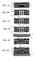
- Fig. 1 is a cross sectional view showing a multi-layer circuit substrate according to an embodiment of the present invention.
- the multi-layer circuit substrate shown in Fig. 1 is provided with a laminated circuit portion 13 formed by laminating alternately conducting layers 11 and insulating layers 12 and also provided with a metal substrate 14.
- the conducting layer 11 is made of a metal
- the insulating layer 12 is formed of a composite in which an insulating resin is impregnated into glass fiber (so-called prepreg). It is preferable that the conducting layer 11 is made of a metal excellent in thermal conductivity, while the insulating layer 12 is made of a resin having the thermal conductivity of 1 W/m ⁇ K or more.
- the conducting layer 11 is to be made of copper and the insulating layer 12 is to be made of a composite of glass fiber and epoxy resin.
- the laminated circuit portion 13 is formed by thermal compression bonding a plurality of conducting layers 11 with a plurality of insulating layers 12.
- the uppermost layer of the laminated circuit portion 13 is a conducting layer 11 and the lowermost layer is an insulating layer 12.
- An electronic component is placed on a conducting layer 11 which is the uppermost layer (refer to Fig. 5 ).
- the uppermost conducting layer 11 is subjected to gold plating 15, with nickel plating undercoated.
- a metal substrate 14 is installed below the laminated circuit portion 13 and a heat dissipating via 21 is installed at the laminated circuit portion 13.
- the metal substrate 14 is made of a metal excellent in thermal conductivity such as aluminum, thereby acting as a heat sink.
- the metal substrate 14 is installed so as to be in contact with an insulating layer 12, which is the lowermost layer.
- the lowermost insulating layer 12 and the metal substrate 14 are thermal compression bonded, by which they can be easily firmly attached.
- Fig. 2 is a plan view and a cross sectional view of a heat dissipating via 21.
- the heat dissipating via 21 is an inter-layer connecting hole formed in the thickness direction of conducting layers 11 and insulating layers 12.
- the heat dissipating via 21 is obtained by forming a conducting layer 22 on the inner surface of a through hole penetrating from an insulating layer immediately below a conducting layer 11, which is the uppermost layer, to a conducting layer immediately above an insulating layer 12, which is the lowermost layer, and filling a resin 23 thereinto.
- the conducting layer 22 is formed by metal plating such as copper plating.
- a resin in this case, a composite of glass fiber and epoxy resin which is the same as that used in forming the insulating layers 12 may be used as the resin 23.
- the thus formed heat dissipating via 21 connects the uppermost conducting layer 11 on which an electronic component is placed with the lowermost insulating layer 12 via the conducting layer 22 formed on the inner surface.
- Electronic components mounted on the multi-layer circuit substrate shown in Fig. 1 include parts great in heating value on operation and parts relatively low in heating value on operation.
- One or any given number of heat dissipating vias 21 are installed at sites where the electronic components great in heating value are mounted, of these parts. Heat generated at the electronic components is transmitted via the uppermost conducting layer 11 and the conducting layer 22 formed on the inner surface of the heat dissipating via 21 down to the lowermost insulating layer 12, and also transmitted from there to the metal substrate 14.
- the heat dissipating via 21 acts to transmit the heat generated at the electronic components to an insulating layer immediately above the metal substrate 14 (more specifically, the lowermost insulating layer) 12 at an excellent thermal conductivity.
- the heat dissipating via 21 is formed so as to penetrate a conducting layer immediately above an insulating layer 12, which is the lowermost layer, but not penetrate an insulating layer 12, which is the lowermost layer. It is, thereby, possible to prevent a conducting layer 11, which is the uppermost layer, from short-circuiting with the other conducting layer 11, which is the uppermost layer, via the metal substrate 14.
- the lowermost insulating layer 12 is installed for preventing the short circuit. It is noted that in order to improve the thermal conductivity, the lowermost insulating layer 12 is preferably as thin as possible, as long as it keeps insulation properties.
- the heat dissipating via 21 shown in Fig. 1 is connected electrically only with a conducting layer 11, which is the uppermost layer.
- the heat dissipating via may be electrically connected with a conducting layer 11 other than the uppermost conducting layer.
- the heat dissipating via 24 is electrically connected also with a third conducting layer 11 (a third layer from above), in addition to the uppermost conducting layer 11.
- the heat dissipating via 24 is a via electrically connecting the uppermost conducting layer 11 with the third conducting layer 11 which is extended so as to penetrate a conducting layer 11 immediately above an insulating layer 12, which is the uppermost layer.
- the via which connects electrically these conducting layers is extended to form a heat dissipating via, thus making it possible to prevent an increase in the substrate area resulting from the installation of heat dissipating vias.
- Figs. 4A to 4F are views showing an example of steps of manufacturing the multi-layer circuit substrate according to the present embodiment.
- steps of manufacturing a multi-layer circuit substrate which is provided with a laminated circuit portion made up of four conducting layers and four insulating layers and also provided with a heat dissipating via connected electrically with the uppermost conducting layer and a third conducting layer.
- the circuit pattern is formed by formation of etching resist or treatment such as etching.
- a hole is made in advance at a site where a heat dissipating via is to be formed on a fifth conducting layer 11, and the prepreg is held and subjected to pressing, thereby the hole made on the conducting layer 11 is filled with a resin.
- the pressing carried out at this time may be conducted in a vacuum state, whenever necessary.
- a hole 25 is made at a site where the heat dissipating via is to be formed on the laminated body 16 except for only a conducting layer 11a, which is the uppermost layer ( Fig. 4B ). More specifically, the hole 25 is made which penetrates through a conducting layer 11b, which is the lowermost layer at this time, to an insulating layer 12a immediately below the conducting layer 11a, which is the uppermost layer. Then, the lower side surface of the laminated body 16 and the inner surface of the hole 25 are subjected to treatment necessary prior to cleaning, thereby giving conductive plating such as copper plating. Thus, a conducting layer 22 is formed on the inner surface of the hole 25 ( Fig. 4C ).
- a circuit pattern is formed on the uppermost conducting layer 11a of the laminated body 16 and a conducting layer 11b, which is the lowermost layer at this time ( Fig. 4D ).
- the circuit pattern is formed by formation of etching resist or treatment such as etching.
- the laminated body 16 is turned over, a resin 23 is filled into the hole 25, on which a resin-made prepreg 12b (this is given as the lowermost insulating layer) and a metal substrate 14 which is subjected to rough surface treatment by an oxidation solution are placed, and the thus treated laminated body is heated and pressurized ( Fig. 4E ).
- the laminated body 16, the insulating layer 12b, and the metal substrate 14 are thermal compression bonded.
- the metal substrate 14 is subjected to rough surface treatment because the lowermost insulating layer 12b is firmly attached to the metal substrate 14.
- the lowermost insulating layer 12b is thermal compression bonded to the seven-ply laminated body 16 to form an eight-ply laminated circuit portion 13.
- the uppermost conducting layer 11 is connected with the lowermost insulating layer 12 by the conducting layer 22 formed on the inner surface to form a heat dissipating via 24 into which the resin 23 is filled.
- the multi-layer circuit substrate according to the present embodiment can be manufactured by the treatment described above.
- the multi-layer circuit substrate according to the present embodiment is applied, for example, to a motor drive circuit substrate for an electric power steering system.
- Fig. 5 is a cross sectional view showing the motor drive circuit substrate including the multi-layer circuit substrate shown in Fig. 1 .
- the motor drive circuit substrate shown in Fig. 5 is used by being built into an ECU (electronic control unit) for an electric power steering system.
- the ECU includes a motor control circuit for calculating an amount of driving electric current supplied to a steering assistance motor and a motor drive circuit for controlling a great electric current to drive the steering assistance motor.
- the motor control circuit will not generate heat in a great amount on operation but the motor drive circuit will generate heat in a relatively great amount on operation.
- the motor drive circuit is mounted on a motor drive circuit substrate ( Fig. 5 ), while the motor control circuit is mounted on another circuit substrate. These two circuit substrates are arranged in parallel or in two stages inside the ECU.
- the motor drive circuit substrate shown in Fig. 5 is a substrate in which an electronic component 31 is placed on a conducting layer 11, which is the uppermost layer, on the multi-layer circuit substrate shown in Fig. 1 .
- the electronic component 31 mounted on the motor drive circuit substrate is provided with a semiconductor chip, a current detecting sensor, a noise removing coil, and relays including a power-off relay and a motor phase-current blocking relay. In addition, all of these electronic components are not necessarily mounted on the motor drive circuit substrate.
- the uppermost conducting layer 11 made of copper is subjected to gold plating 15, with nickel plating undercoated, it is possible to solder the electronic component 31 to the uppermost conducting layer 11.
- a semiconductor chip is preferably mounted as a bare chip.
- a reflow soldering is preferably conducted in a vacuum. Thereby, melted solder is prevented from being mixed with air bubbles to improve the thermal conductivity between the electronic component 31 and the uppermost conducting layer 11.
- heat dissipating vias are installed at sites where electronic components 31 are arranged.
- an electronic component 31 is soldered to the uppermost conducting layer 11
- a heat dissipating via (such as the heat dissipating via 21 shown in Fig. 1 ) is installed which is electrically connected only with the uppermost conducting layer 11.
- a heat dissipating via (such as the heat dissipating via 24 shown in Fig.
- the motor drive circuit substrate shown in Fig. 5 is provided with a metal substrate 14, a hole for tightening screws is made in the metal substrate 14, thereby a substrate can be screwed to a case of the ECU, unlike the ceramic multi-layer substrate.
- the uppermost conducting layer 11 is subjected to gold plating 15, with nickel plating undercoated.
- the uppermost conducting layer 11 and the external connecting terminal can be subjected to wire bonding by using an aluminum wire.
- the multi-layer circuit substrate according to the present embodiment is formed by laminating conducting layers and resin-made insulating layers, it can be manufactured at a lower cost than a ceramic multi-layer substrate in which ceramic substrates are laminated. Further, since the multi-layer circuit substrate according to the present embodiment is provided with a heat dissipating via, heat generated on an electronic component is transmitted at an excellent thermal conductivity via the heat dissipating via to a metal substrate. As described above, the present embodiment is able to provide a multi-layer circuit substrate which is lower in cost and excellent in thermal conductivity.
- a resin is filled into the heat dissipating via on the multi-layer circuit substrate according to the present embodiment. Since a resin has the nature of being easily filled, a step for making a hole, a step for metal plating and a step for filling a resin are carried out once with respect to a laminated circuit portion, thus making it possible to form the heat dissipating via. On the other hand, in order to fill a metal paste or the like in a heat dissipating via, it is necessary to carry out a step for making a hole, a step for metal plating and a step for filling a metal paste repeatedly in the course of forming a laminated circuit portion. As described above, the present embodiment is able to form the heat dissipating via in simple steps.
- the conducting layers and the resin-made insulating layers are thermal compression bonded, thus making it possible to form a laminated circuit portion easily in the existing steps.
- An insulating layer, which is the lowermost layer, and a metal substrate are also thermal compression bonded, by which the metal substrate can be firmly attached to the lowermost insulating layer easily. Copper which is excellent in thermal conductivity is used to constitute the conducting layers and a heat dissipating via, by which a multi-layer circuit substrate can be improved in thermal conductivity.
- a copper-made conducting layer, which is the uppermost layer is subjected to gold plating, with nickel plating undercoated, thus making it possible to solder the uppermost conducting layer and also carry out aluminum wire bonding.
- the motor drive circuit substrate according to the present embodiment is mounted with an electronic component for driving a motor on a multi-layer circuit substrate excellent in thermal conductivity at a low cost, it is lower in cost, and excellent in thermal conductivity and small in substrate area. Further, the motor drive circuit substrate according to the present embodiment is provided with a metal substrate. Thus, a hole for tightening screws is made in the metal substrate, by which the metal substrate can be screwed to a case of an ECU.
- the conducting layers 11 are made of copper.
- the conducting layers may be made of metals such as aluminum, nickel, silver, titanium and gold, their alloys the surface of which is laminated by plating with nickel or nickel/gold.
- these metals, alloys and laminated films may be formed by pressure bonding, sputtering, chemical vapor deposition, vacuum deposition, thick film printing or a combination of these methods.
- the thick film printing is preferable, with consideration given to the fact that the conducting layers 11 are approximately 100 ⁇ m in thickness.
- the DLC layer is made up of an inclined DLC layer in which the silicon containing concentration varies sequentially and a DLC layer is free of silicon.
- the inclined DLC layer is formed on a metal substrate on which a chromium layer or a titanium layer is in advance formed and the DLC layer free of silicon is then formed.
- the inclined DLC layer is higher in silicon content on the chromium layer (or the titanium layer) (10 to 20at%, for example), gradually lower in silicon content as it moves away from the chromium layer or the titanium layer, and lowest on the inclined DLC layer free of silicon (0-4at%, for example).
- the insulating layer 12 can be made extremely thin or as thin as from 1 to 2 ⁇ m in thickness to decrease the thermal resistance. Therefore, heat generated from electronic components can be transmitted via heat dissipating vias 21 and 24 at an excellent thermal conductivity to a metal substrate 14.
- the chromium layer (or the titanium layer) and the inclined DLC layer are held between the metal substrate 14 and the DLC layer free of silicon due to a reason that they are improved in adhesiveness between these layers.
- a chromium nitride layer may be additionally formed between the chromium layer and the inclined DLC layer. In this case, the DLC layer can be prevented from collapse even on application of a high contact pressure.
- the motor drive circuit substrate according to the present embodiment may be fixed by thermal compression bonding the insulating layer 12, which is the lowermost layer, on the laminated circuit portion 13 to a case of an ECU or a metallic housing such as a gear housing.
- the necessity for applying thermal grease to decrease the thermal resistance of the substrate 14 against the metal housing or for polishing to improve the surface roughness of the metal substrate 14 can be eliminated, thus making it possible to reduce the cost of manufacturing the motor drive circuit substrate.
- the necessity for screwing on a housing the metal substrate 14 which supports the laminated circuit portion 13 can be eliminated, thereby eliminating the necessity for making a clearance for tightening screws.
- the motor drive circuit substrate can be downsized accordingly
- the metal substrate 14 acts to support the laminated circuit portion 13 as well.
- the laminated circuit portion 13 is usually 1 mm or more in thickness, the laminated circuit portion 13 can be easily handled without the metal substrate 14, when thermal compression bonding to the housing.
- a substrate capable of acting as a heat sink may be used as the metal substrate 54, and, for example, a case of an ECU is acceptable.
- a thin film such as a chromium layer or a titanium layer is formed in advance on the metal substrate 54 by sputtering or others.
- an inclined DLC layer which is higher in silicon content on the chromium layer (or the titanium layer) (10 to 20at%, for example), gradually lower as it moves away from the chromium layer or the titanium layer and lowest at the end (0 to 4at%, for example). Then, a DLC free of silicon is formed thereon. Since the thus formed film of the insulating layer 52 is quite thin, for example, 1 to 2 ⁇ m in thickness, the thermal resistance is decreased and heat generated at an electronic component 61 can be transmitted at an excellent thermal conductivity to the metal substrate 54. Further, a chromium nitride layer may be additionally formed between the chromium layer and the inclined DLC layer. In this case, the DLC layer can be prevented from collapse even when a high contact pressure is applied.
- the conducting layer 51 is formed on the surface of the insulating layer 52.
- the conducting layer 51 is made of copper, aluminum, nickel, silver, titanium, gold, an alloy of two or more of these metals or their alloys the surface of which is plated with nickel or nickel/gold. Further, these metals and others may be formed by pressure bonding, sputtering, chemical vapor deposition, vacuum deposition or thick film printing or a combination of these methods. The thick film printing is preferable, with consideration given to the fact that the conducting layer 51 is approximately 100 ⁇ m in thickness.
- the conducting layer 51 is subjected to gold plating 55, with nickel plating undercoated and, thereafter, an electronic component 61 is mounted on the surface of the conducting layer 51.
- an electronic component 61 is mounted on the surface of the conducting layer 51.
- the electronic component 61, the conducting layer 51 and the external connecting terminal 62 are respectively subjected to wire bonding by using an aluminum wire 60.
Landscapes
- Engineering & Computer Science (AREA)
- Microelectronics & Electronic Packaging (AREA)
- Production Of Multi-Layered Print Wiring Board (AREA)
- Cooling Or The Like Of Semiconductors Or Solid State Devices (AREA)
- Power Steering Mechanism (AREA)
- Structure Of Printed Boards (AREA)
Abstract
Description
- The present invention relates to a multi-layer circuit substrate and a motor drive circuit substrate for an electric power steering system using the multi-layer circuit substrate.
- An electric power steering system for a vehicle drives a steering assistance motor so as to obtain an appropriate steering assistance power, depending on the steering torque provided through a steering wheel operated by a driver and the speed of the vehicle. The steering assistance motor is driven by a motor drive circuit built in an electronic control unit (hereinafter abbreviated as ECU). The motor drive circuit controls a large electric power of approximately 500W to 2000W when driving the steering assistance motor.
- At this time, the motor drive circuit generates heat. In order to prevent a malfunction or a breakdown of the ECU resulting from the heat generation, the motor drive circuit is mounted on a circuit substrate excellent in thermal conductivity. The motor drive circuit is mounted on a metallic circuit substrate which forms one layer of a copper-made conducting
layer 91 and one layer of a resin-madeinsulating layer 92 on a metal substrate 93 (heat sink) made of aluminum, for example, as shown in Pig. 7(a). - Since electronic components are allowed to be mounted only on one side of the circuit substrate shown in
Fig. 7(a) (more specifically, on the conducting layer 91), the circuit substrate occupying area becomes large in the ECU. Thus, as a method for reducing a substrate area, a method for making a circuit substrate multi-layered can be considered. However, when the circuit substrate shown inFig. 7(a) is simply multi-layered, a resin-made insulating layer poor in thermal conductivity is overlaid. As a result, heat generated by electronic components is less likely to be transmitted to themetal substrate 93. - In order to solve the above problem, mounting a motor drive circuit which is mounted on a ceramic multi-layer substrate has been proposed. The ceramic multi-layer substrate shown in
Fig. 7(b) is obtained by laminating copper-made conductinglayers 91 on ceramicinsulating layers 94 to give a multiple layer, and bonding it to an aluminum metal substrate 93 (heat sink) with anadhesive agent 95. This ceramic multi-layer substrate is able to constitute a circuit conductor between the ceramic insulating layers so as to reduce a substrate area. - It is noted that the following prior art is known about the present invention. Japanese Published Unexamined Patent Application No.
9-153679 2004-363183 2004-79883 - As described above, a ceramic multi-layer substrate has features including an excellent thermal conductivity and a small substrate area. However, the ceramic multi-layer substrate is higher in cost, which poses a problem. Further, because the ceramic multi-layer substrate easily cracks, a problem arises that a method is required other than fixing the inside of the ECU with a screw.
- In view of the above situation, an object of the present invention is to provide a multi-layer circuit substrate which is lower in cost and excellent in thermal conductivity.
- A first aspect of the invention is a multi-layer circuit substrate comprising: a laminated circuit portion in which conducting layers and resin-made insulating layers are alternately laminated; a metal substrate provided so as to be in contact with the lowermost insulating layer; and a heat dissipating via which connects the uppermost conducting layer on which an electronic component is placed with the lowermost insulating layer by using a conducting layer formed on an inner surface of the heat dissipating via.
- A second aspect of the invention is characterized in that, in the first aspect of the invention, a resin is filled in the heat dissipating via.
- A third aspect of the invention is characterized in that, in the first aspect of the invention, the laminated circuit portion is formed by thermal compression bonding the conducting layers and the resin-made insulating layers.
- A fourth aspect of the invention is characterized in that, in the first aspect of the invention, the lowermost insulating layer and the metal substrate are thermal compression bonded.
- A fifth aspect of the invention is characterized in that, in the first aspect of the invention, the conducting layer of the laminated circuit portion and the conducting layer formed on the inner surface of the heat dissipating via are made of copper.
- A sixth aspect of the invention is characterized in that, in the firth aspect of the invention, the uppermost conducting layer is subjected to gold plating, with nickel plating undercoated.
- A seventh aspect of the invention is characterized in that a motor drive circuit substrate for an electric power steering system comprising a multi-layer circuit substrate comprising a laminated circuit portion in which conducting layers and resin-made insulating layers are alternately laminated, a metal substrate provided so as to be in contact with the lowermost insulating layer, and a heat dissipating via which connects the uppermost conducting layer on which an electronic component is placed with the lowermost insulating layer by using a conducting layer formed on an inner surface of the heat dissipating via; and an electronic component placed on the uppermost conducting layer.
- According to the first aspect of the invention, the conducting layers and the resin-made insulating layers are laminated, thus making it possible to constitute a multi-layer circuit substrate at a lower cost than a ceramic multi-layer substrate. Further, heat generated at the electronic component is transmitted at a high thermal conductivity via the heat dissipating via to the metal substrate. Therefore, it is possible to obtain the multi-layer circuit substrate lower in cost and excellent in thermal conductivity.
- According to the second aspect of the invention, since a resin has the nature of being easily filled, a step for making a hole, a step for forming conducting layers and a step for filling the resin are carried out once with respect to the laminated circuit portion, thus making it possible to form the heat dissipating via. It is, therefore, possible to form the heat dissipating via more easily than a case where a metal paste or the like is filled.
- According to the third aspect of the invention, since the conducting layers and the resin-made insulating layers are thermal compression bonded, it is possible to form easily the laminated circuit portion by using the existing steps.
- According to the fourth aspect of the invention, since the lowermost insulating layer and the metal substrate are thermal compression bonded, it is possible to attach the metal substrate firmly to the lowermost insulating layer easily.
- According to the fifth aspect of the invention, copper which is excellent in thermal conductivity is used to constitute the conducting layers and the heat dissipating via, thus making it possible to improve the thermal conductivity of the multi-layer circuit substrate.
- According to the sixth aspect of the invention, the copper-made uppermost conducting layer is subjected to gold plating, with nickel plating undercoated, thus making it possible to solder the uppermost conducting layer and provide aluminum wire bonding.
- According to the seventh aspect of the invention, the electronic component is mounted on the multi-layer circuit substrate lower in cost and excellent in thermal conductivity, by which it is possible to obtain a motor drive circuit substrate which is lower in cost, excellent in thermal conductivity and small in substrate area. Further, a hole for tightening screws is made in the metal substrate to screw the multi-layer circuit substrate to a case.
-
-
Fig. 1 is a cross sectional view showing a multi-layer circuit substrate according to an embodiment of the present invention. -
Fig. 2 is a plan view and a cross sectional view showing a heat dissipating via included in the multi-layer circuit substrate shown inFig. 1 . -
Fig. 3 is a cross sectional view of another example of the multi-layer circuit substrate according to an embodiment of the present invention. -
Figs. 4A to 4F are views showing an example of steps of manufacturing the multi-layer circuit substrate shown inFig. 1 . -
Fig. 5 is a cross sectional view showing a motor drive circuit substrate including the multi-layer circuit substrate shown in theFig. 1 . -
Fig. 6 is a cross sectional view showing a motor drive circuit substrate including a single layer circuit substrate. -
Fig. 7 is a cross sectional view showing a conventional circuit substrate. -
- 11: Conducting layer
- 12: Insulating layer
- 13: Laminated circuit portion
- 14: Metal substrate
- 15: Gold plating, with nickel plating undercoated
- 16: Laminated body
- 21, 24: Heat dissipating via
- 22: Conducting layer
- 23: Resin
- 25: Hole
- 31: Electronic component
-
Fig. 1 is a cross sectional view showing a multi-layer circuit substrate according to an embodiment of the present invention. The multi-layer circuit substrate shown inFig. 1 is provided with alaminated circuit portion 13 formed by laminating alternately conductinglayers 11 and insulatinglayers 12 and also provided with ametal substrate 14. The conductinglayer 11 is made of a metal, while the insulatinglayer 12 is formed of a composite in which an insulating resin is impregnated into glass fiber (so-called prepreg). It is preferable that the conductinglayer 11 is made of a metal excellent in thermal conductivity, while the insulatinglayer 12 is made of a resin having the thermal conductivity of 1 W/m·K or more. In the following description, the conductinglayer 11 is to be made of copper and the insulatinglayer 12 is to be made of a composite of glass fiber and epoxy resin. - The
laminated circuit portion 13 is formed by thermal compression bonding a plurality of conductinglayers 11 with a plurality of insulatinglayers 12. The uppermost layer of thelaminated circuit portion 13 is aconducting layer 11 and the lowermost layer is an insulatinglayer 12. An electronic component is placed on aconducting layer 11 which is the uppermost layer (refer toFig. 5 ). In order to solder the electronic component to the copper-madeuppermost conducting layer 11, theuppermost conducting layer 11 is subjected togold plating 15, with nickel plating undercoated. - Further, in order to release the heat generated in the electronic component, a
metal substrate 14 is installed below thelaminated circuit portion 13 and a heat dissipating via 21 is installed at thelaminated circuit portion 13. Themetal substrate 14 is made of a metal excellent in thermal conductivity such as aluminum, thereby acting as a heat sink. Themetal substrate 14 is installed so as to be in contact with an insulatinglayer 12, which is the lowermost layer. The lowermost insulatinglayer 12 and themetal substrate 14 are thermal compression bonded, by which they can be easily firmly attached. -
Fig. 2 is a plan view and a cross sectional view of a heat dissipating via 21. The heat dissipating via 21 is an inter-layer connecting hole formed in the thickness direction of conductinglayers 11 and insulatinglayers 12. In more detail, the heat dissipating via 21 is obtained by forming aconducting layer 22 on the inner surface of a through hole penetrating from an insulating layer immediately below a conductinglayer 11, which is the uppermost layer, to a conducting layer immediately above an insulatinglayer 12, which is the lowermost layer, and filling aresin 23 thereinto. The conductinglayer 22 is formed by metal plating such as copper plating. A resin (in this case, a composite of glass fiber and epoxy resin) which is the same as that used in forming the insulatinglayers 12 may be used as theresin 23. The thus formed heat dissipating via 21 connects theuppermost conducting layer 11 on which an electronic component is placed with the lowermost insulatinglayer 12 via theconducting layer 22 formed on the inner surface. - Electronic components mounted on the multi-layer circuit substrate shown in
Fig. 1 include parts great in heating value on operation and parts relatively low in heating value on operation. One or any given number ofheat dissipating vias 21 are installed at sites where the electronic components great in heating value are mounted, of these parts. Heat generated at the electronic components is transmitted via theuppermost conducting layer 11 and theconducting layer 22 formed on the inner surface of the heat dissipating via 21 down to the lowermost insulatinglayer 12, and also transmitted from there to themetal substrate 14. The heat dissipating via 21 acts to transmit the heat generated at the electronic components to an insulating layer immediately above the metal substrate 14 (more specifically, the lowermost insulating layer) 12 at an excellent thermal conductivity. - The heat dissipating via 21 is formed so as to penetrate a conducting layer immediately above an insulating
layer 12, which is the lowermost layer, but not penetrate an insulatinglayer 12, which is the lowermost layer. It is, thereby, possible to prevent aconducting layer 11, which is the uppermost layer, from short-circuiting with theother conducting layer 11, which is the uppermost layer, via themetal substrate 14. The lowermost insulatinglayer 12 is installed for preventing the short circuit. It is noted that in order to improve the thermal conductivity, the lowermost insulatinglayer 12 is preferably as thin as possible, as long as it keeps insulation properties. - The heat dissipating via 21 shown in
Fig. 1 is connected electrically only with aconducting layer 11, which is the uppermost layer. However, the heat dissipating via may be electrically connected with aconducting layer 11 other than the uppermost conducting layer. For example, as shown inFig. 3 , the heat dissipating via 24 is electrically connected also with a third conducting layer 11 (a third layer from above), in addition to theuppermost conducting layer 11. The heat dissipating via 24 is a via electrically connecting theuppermost conducting layer 11 with thethird conducting layer 11 which is extended so as to penetrate aconducting layer 11 immediately above an insulatinglayer 12, which is the uppermost layer. As described above, the via which connects electrically these conducting layers is extended to form a heat dissipating via, thus making it possible to prevent an increase in the substrate area resulting from the installation of heat dissipating vias. -
Figs. 4A to 4F are views showing an example of steps of manufacturing the multi-layer circuit substrate according to the present embodiment. Here, as an example, a description will be given for steps of manufacturing a multi-layer circuit substrate which is provided with a laminated circuit portion made up of four conducting layers and four insulating layers and also provided with a heat dissipating via connected electrically with the uppermost conducting layer and a third conducting layer. - First, in the same procedures as those for manufacturing a copper-plated laminated plate, four conducting
layers 11 and three sheets of prepregs (those in which an insulating resin is impregnated into a glass cloth), which are given as resin-madeinsulating layers 12, are alternately laminated, and the copper surface to be in contact with the prepreg is subjected to treatment prior to lamination by using an alkaline oxidation solution (for example, NaClO2 or NaOH), which is further subjected to heating and pressing. Thereby, a seven-ply laminated body 16 (Fig. 4A ) is formed. However, before the pressing, a circuit pattern is formed on conductinglayers 11, which are given as inner layers, (a third and fifth conducting layers in this example), whenever necessary. As publicly known, the circuit pattern is formed by formation of etching resist or treatment such as etching. InFig. 4A , a hole is made in advance at a site where a heat dissipating via is to be formed on afifth conducting layer 11, and the prepreg is held and subjected to pressing, thereby the hole made on theconducting layer 11 is filled with a resin. The pressing carried out at this time may be conducted in a vacuum state, whenever necessary. - Next, a
hole 25 is made at a site where the heat dissipating via is to be formed on thelaminated body 16 except for only aconducting layer 11a, which is the uppermost layer (Fig. 4B ). More specifically, thehole 25 is made which penetrates through aconducting layer 11b, which is the lowermost layer at this time, to an insulatinglayer 12a immediately below theconducting layer 11a, which is the uppermost layer. Then, the lower side surface of thelaminated body 16 and the inner surface of thehole 25 are subjected to treatment necessary prior to cleaning, thereby giving conductive plating such as copper plating. Thus, a conductinglayer 22 is formed on the inner surface of the hole 25 (Fig. 4C ). Further, a circuit pattern is formed on theuppermost conducting layer 11a of thelaminated body 16 and aconducting layer 11b, which is the lowermost layer at this time (Fig. 4D ). As publicly known, the circuit pattern is formed by formation of etching resist or treatment such as etching. - After that, the
laminated body 16 is turned over, aresin 23 is filled into thehole 25, on which a resin-madeprepreg 12b (this is given as the lowermost insulating layer) and ametal substrate 14 which is subjected to rough surface treatment by an oxidation solution are placed, and the thus treated laminated body is heated and pressurized (Fig. 4E ). Thereby, thelaminated body 16, the insulatinglayer 12b, and themetal substrate 14 are thermal compression bonded. Themetal substrate 14 is subjected to rough surface treatment because the lowermost insulatinglayer 12b is firmly attached to themetal substrate 14. The lowermost insulatinglayer 12b is thermal compression bonded to the seven-ply laminatedbody 16 to form an eight-ply laminatedcircuit portion 13. By the treatment so far given, theuppermost conducting layer 11 is connected with the lowermost insulatinglayer 12 by the conductinglayer 22 formed on the inner surface to form a heat dissipating via 24 into which theresin 23 is filled. - Finally, the thermal compression bonded
laminated circuit portion 13 and themetal substrate 14 are again turned over, theuppermost conducting layer 11 is subjected to necessary prior treatment and subjected togold plating 15, with nickel plating undercoated (Fig. 4F ). The multi-layer circuit substrate according to the present embodiment can be manufactured by the treatment described above. - The multi-layer circuit substrate according to the present embodiment is applied, for example, to a motor drive circuit substrate for an electric power steering system.
Fig. 5 is a cross sectional view showing the motor drive circuit substrate including the multi-layer circuit substrate shown inFig. 1 . The motor drive circuit substrate shown inFig. 5 is used by being built into an ECU (electronic control unit) for an electric power steering system. - The ECU includes a motor control circuit for calculating an amount of driving electric current supplied to a steering assistance motor and a motor drive circuit for controlling a great electric current to drive the steering assistance motor. The motor control circuit will not generate heat in a great amount on operation but the motor drive circuit will generate heat in a relatively great amount on operation. The motor drive circuit is mounted on a motor drive circuit substrate (
Fig. 5 ), while the motor control circuit is mounted on another circuit substrate. These two circuit substrates are arranged in parallel or in two stages inside the ECU. - The motor drive circuit substrate shown in
Fig. 5 is a substrate in which anelectronic component 31 is placed on aconducting layer 11, which is the uppermost layer, on the multi-layer circuit substrate shown inFig. 1 . Theelectronic component 31 mounted on the motor drive circuit substrate is provided with a semiconductor chip, a current detecting sensor, a noise removing coil, and relays including a power-off relay and a motor phase-current blocking relay. In addition, all of these electronic components are not necessarily mounted on the motor drive circuit substrate. - Since the
uppermost conducting layer 11 made of copper is subjected togold plating 15, with nickel plating undercoated, it is possible to solder theelectronic component 31 to theuppermost conducting layer 11. In this case, in order to decrease a substrate area, a semiconductor chip is preferably mounted as a bare chip. Further, on soldering, a reflow soldering is preferably conducted in a vacuum. Thereby, melted solder is prevented from being mixed with air bubbles to improve the thermal conductivity between theelectronic component 31 and theuppermost conducting layer 11. - One or any given number of heat dissipating vias are installed at sites where
electronic components 31 are arranged. When anelectronic component 31 is soldered to theuppermost conducting layer 11, there is a case where a terminal of theelectronic component 31 is soldered and a case where a part other than the terminal of the electronic component 31 (for example, the back surface of a semiconductor chip) is soldered. In the latter case, a heat dissipating via (such as the heat dissipating via 21 shown inFig. 1 ) is installed which is electrically connected only with theuppermost conducting layer 11. In the former case, a heat dissipating via (such as the heat dissipating via 24 shown inFig. 3 ) is installed which is electrically connected with aconducting layer 11 other than the uppermost layer. It is not necessary to install heat dissipating vias at all sites whereelectronic components 31 are arranged. On the motor drive circuit substrate shown inFig. 5 , no heat dissipating via is installed at a site where theelectronic component 31 on the right side is arranged. - Since the motor drive circuit substrate shown in
Fig. 5 is provided with ametal substrate 14, a hole for tightening screws is made in themetal substrate 14, thereby a substrate can be screwed to a case of the ECU, unlike the ceramic multi-layer substrate. Further, theuppermost conducting layer 11 is subjected togold plating 15, with nickel plating undercoated. Thus, when an external connecting terminal installed on the case of the ECU is electrically connected, theuppermost conducting layer 11 and the external connecting terminal can be subjected to wire bonding by using an aluminum wire. - Hereinafter, a description will be given for effects of the multi-layer circuit substrate and the motor drive circuit substrate according to the present embodiment. Since the multi-layer circuit substrate according to the present embodiment is formed by laminating conducting layers and resin-made insulating layers, it can be manufactured at a lower cost than a ceramic multi-layer substrate in which ceramic substrates are laminated. Further, since the multi-layer circuit substrate according to the present embodiment is provided with a heat dissipating via, heat generated on an electronic component is transmitted at an excellent thermal conductivity via the heat dissipating via to a metal substrate. As described above, the present embodiment is able to provide a multi-layer circuit substrate which is lower in cost and excellent in thermal conductivity.
- Further, a resin is filled into the heat dissipating via on the multi-layer circuit substrate according to the present embodiment. Since a resin has the nature of being easily filled, a step for making a hole, a step for metal plating and a step for filling a resin are carried out once with respect to a laminated circuit portion, thus making it possible to form the heat dissipating via. On the other hand, in order to fill a metal paste or the like in a heat dissipating via, it is necessary to carry out a step for making a hole, a step for metal plating and a step for filling a metal paste repeatedly in the course of forming a laminated circuit portion. As described above, the present embodiment is able to form the heat dissipating via in simple steps.
- Still further, the conducting layers and the resin-made insulating layers are thermal compression bonded, thus making it possible to form a laminated circuit portion easily in the existing steps. An insulating layer, which is the lowermost layer, and a metal substrate are also thermal compression bonded, by which the metal substrate can be firmly attached to the lowermost insulating layer easily. Copper which is excellent in thermal conductivity is used to constitute the conducting layers and a heat dissipating via, by which a multi-layer circuit substrate can be improved in thermal conductivity. Further, a copper-made conducting layer, which is the uppermost layer, is subjected to gold plating, with nickel plating undercoated, thus making it possible to solder the uppermost conducting layer and also carry out aluminum wire bonding.
- In addition, since the motor drive circuit substrate according to the present embodiment is mounted with an electronic component for driving a motor on a multi-layer circuit substrate excellent in thermal conductivity at a low cost, it is lower in cost, and excellent in thermal conductivity and small in substrate area. Further, the motor drive circuit substrate according to the present embodiment is provided with a metal substrate. Thus, a hole for tightening screws is made in the metal substrate, by which the metal substrate can be screwed to a case of an ECU.
- In the present embodiment, a description was given for a case where the conducting layers 11 are made of copper. In place of copper, the conducting layers may be made of metals such as aluminum, nickel, silver, titanium and gold, their alloys the surface of which is laminated by plating with nickel or nickel/gold. Further, these metals, alloys and laminated films may be formed by pressure bonding, sputtering, chemical vapor deposition, vacuum deposition, thick film printing or a combination of these methods. The thick film printing is preferable, with consideration given to the fact that the conducting layers 11 are approximately 100 □m in thickness.
- In the present embodiment, a description was given for a case where all insulating
layers 12 inside thelaminated circuit portion 13 are made of a prepreg. It is acceptable that only an insulatinglayer 12, which is the lowermost layer, is made of a diamond like carbon layer (DLC layer). In this case, the DLC layer is made up of an inclined DLC layer in which the silicon containing concentration varies sequentially and a DLC layer is free of silicon. First, the inclined DLC layer is formed on a metal substrate on which a chromium layer or a titanium layer is in advance formed and the DLC layer free of silicon is then formed. The inclined DLC layer is higher in silicon content on the chromium layer (or the titanium layer) (10 to 20at%, for example), gradually lower in silicon content as it moves away from the chromium layer or the titanium layer, and lowest on the inclined DLC layer free of silicon (0-4at%, for example). In this case, the insulatinglayer 12 can be made extremely thin or as thin as from 1 to 2 □m in thickness to decrease the thermal resistance. Therefore, heat generated from electronic components can be transmitted viaheat dissipating vias metal substrate 14. Here, the chromium layer (or the titanium layer) and the inclined DLC layer are held between themetal substrate 14 and the DLC layer free of silicon due to a reason that they are improved in adhesiveness between these layers. Further, a chromium nitride layer may be additionally formed between the chromium layer and the inclined DLC layer. In this case, the DLC layer can be prevented from collapse even on application of a high contact pressure. - Further, the motor drive circuit substrate according to the present embodiment may be fixed by thermal compression bonding the insulating
layer 12, which is the lowermost layer, on thelaminated circuit portion 13 to a case of an ECU or a metallic housing such as a gear housing. In this case, the necessity for applying thermal grease to decrease the thermal resistance of thesubstrate 14 against the metal housing or for polishing to improve the surface roughness of themetal substrate 14 can be eliminated, thus making it possible to reduce the cost of manufacturing the motor drive circuit substrate. The necessity for screwing on a housing themetal substrate 14 which supports thelaminated circuit portion 13 can be eliminated, thereby eliminating the necessity for making a clearance for tightening screws. By just that much, the motor drive circuit substrate can be downsized accordingly In addition, themetal substrate 14 acts to support thelaminated circuit portion 13 as well. However, since thelaminated circuit portion 13 is usually 1 mm or more in thickness, thelaminated circuit portion 13 can be easily handled without themetal substrate 14, when thermal compression bonding to the housing. - As shown in
Fig. 6 , a description will be given for a motor drive circuit substrate in which an insulatinglayer 52 made up of a DLC is formed on a metal substrate 54 made of aluminum and ametal conducting layer 51 is formed thereon. Any substrate capable of acting as a heat sink may be used as the metal substrate 54, and, for example, a case of an ECU is acceptable. A thin film such as a chromium layer or a titanium layer is formed in advance on the metal substrate 54 by sputtering or others. Thereafter, formed is an inclined DLC layer which is higher in silicon content on the chromium layer (or the titanium layer) (10 to 20at%, for example), gradually lower as it moves away from the chromium layer or the titanium layer and lowest at the end (0 to 4at%, for example). Then, a DLC free of silicon is formed thereon. Since the thus formed film of the insulatinglayer 52 is quite thin, for example, 1 to 2 □m in thickness, the thermal resistance is decreased and heat generated at anelectronic component 61 can be transmitted at an excellent thermal conductivity to the metal substrate 54. Further, a chromium nitride layer may be additionally formed between the chromium layer and the inclined DLC layer. In this case, the DLC layer can be prevented from collapse even when a high contact pressure is applied. - Then, the conducting
layer 51 is formed on the surface of the insulatinglayer 52. The conductinglayer 51 is made of copper, aluminum, nickel, silver, titanium, gold, an alloy of two or more of these metals or their alloys the surface of which is plated with nickel or nickel/gold. Further, these metals and others may be formed by pressure bonding, sputtering, chemical vapor deposition, vacuum deposition or thick film printing or a combination of these methods. The thick film printing is preferable, with consideration given to the fact that the conductinglayer 51 is approximately 100 □m in thickness. - Further, as shown in
Fig. 6 , the conductinglayer 51 is subjected togold plating 55, with nickel plating undercoated and, thereafter, anelectronic component 61 is mounted on the surface of the conductinglayer 51. In order to electrically connect electronic components with theother conducting layer 51 and an external connectingterminal 62 installed on the metal substrate 54 such as a case of an ECU, theelectronic component 61, the conductinglayer 51 and the external connectingterminal 62 are respectively subjected to wire bonding by using analuminum wire 60.
Claims (7)
- A multi-layer circuit substrate comprising:a laminated circuit portion in which conducting layers and resin-made insulating layers are alternately laminated;a metal substrate provided so as to be in contact with the lowermost insulating layer; anda heat dissipating via which connects the uppermost conducting layer on which an electronic component is placed with the lowermost insulating layer by using a conducting layer formed on an inner surface of the heat dissipating via.
- The multi-layer circuit substrate according to claim 1, wherein a resin is filled in the heat dissipating via.
- The multi-layer circuit substrate according to claim 1, wherein the laminated circuit portion is formed by thermal compression bonding the conducting layers and the resin-made insulating layers.
- The multi-layer circuit substrate according to claim 1, wherein the lowermost insulating layer and the metal substrate are thermal compression bonded.
- The multi-layer circuit substrate according to claim 1, wherein the conducting layer of the laminated circuit portion and the conducting layer formed on the inner surface of the heat dissipating via are made of copper.
- The multi-layer circuit substrate according to claim 1, wherein the uppermost conducting layer is subjected to gold plating with nickel plating undercoated.
- A motor drive circuit substrate for an electric power steering system comprising:a multi-layer circuit substrate comprising a laminated circuit portion in which conducting layers and resin-made insulating layers are alternately laminated, a metal substrate provided so as to be in contact with the lowermost insulating layer, and a heat dissipating via which connects the uppermost conducting layer on which an electronic component is placed with the lowermost insulating layer by using a conducting layer formed on an inner surface of the heat dissipating via; andan electronic component placed on the uppermost conducting layer.
Applications Claiming Priority (3)
| Application Number | Priority Date | Filing Date | Title |
|---|---|---|---|
| JP2006348738 | 2006-12-26 | ||
| JP2007227937A JP4962228B2 (en) | 2006-12-26 | 2007-09-03 | Multi-layer circuit board and motor drive circuit board |
| PCT/JP2007/074828 WO2008078739A1 (en) | 2006-12-26 | 2007-12-25 | Multilayer circuit board and motor drive circuit board |
Publications (3)
| Publication Number | Publication Date |
|---|---|
| EP2104408A1 true EP2104408A1 (en) | 2009-09-23 |
| EP2104408A4 EP2104408A4 (en) | 2010-05-19 |
| EP2104408B1 EP2104408B1 (en) | 2012-02-15 |
Family
ID=39562528
Family Applications (1)
| Application Number | Title | Priority Date | Filing Date |
|---|---|---|---|
| EP07860057A Not-in-force EP2104408B1 (en) | 2006-12-26 | 2007-12-25 | Multilayer circuit board and motor drive circuit board |
Country Status (6)
| Country | Link |
|---|---|
| US (1) | US20090260858A1 (en) |
| EP (1) | EP2104408B1 (en) |
| JP (1) | JP4962228B2 (en) |
| CN (1) | CN101606446B (en) |
| AT (1) | ATE546034T1 (en) |
| WO (1) | WO2008078739A1 (en) |
Cited By (1)
| Publication number | Priority date | Publication date | Assignee | Title |
|---|---|---|---|---|
| DE102012215788A1 (en) * | 2012-09-06 | 2014-03-06 | Osram Gmbh | Multi-layer LED printed circuit board |
Families Citing this family (38)
| Publication number | Priority date | Publication date | Assignee | Title |
|---|---|---|---|---|
| KR100825766B1 (en) * | 2007-04-26 | 2008-04-29 | 한국전자통신연구원 | LTC package and manufacturing method |
| JP4764393B2 (en) * | 2007-09-06 | 2011-08-31 | 三菱重工業株式会社 | Inverter-integrated electric compressor |
| JP5444619B2 (en) * | 2008-02-07 | 2014-03-19 | 株式会社ジェイテクト | Multi-layer circuit board and motor drive circuit board |
| JP2010073767A (en) | 2008-09-17 | 2010-04-02 | Jtekt Corp | Multilayer circuit board |
| JP5417804B2 (en) * | 2008-11-06 | 2014-02-19 | 株式会社ジェイテクト | Bubble rate calculation method and bubble rate calculation device |
| JP5262619B2 (en) * | 2008-11-25 | 2013-08-14 | 株式会社ジェイテクト | Composite circuit board for motor drive |
| US8248803B2 (en) * | 2010-03-31 | 2012-08-21 | Hong Kong Applied Science and Technology Research Institute Company Limited | Semiconductor package and method of manufacturing the same |
| CN101853822B (en) * | 2010-04-14 | 2012-01-25 | 星弧涂层科技(苏州工业园区)有限公司 | Novel heat sink and production method thereof |
| JP2012009828A (en) | 2010-05-26 | 2012-01-12 | Jtekt Corp | Multilayer circuit board |
| JP2011253890A (en) * | 2010-06-01 | 2011-12-15 | Jtekt Corp | Method of manufacturing multilayer circuit board |
| WO2012071795A1 (en) * | 2010-11-30 | 2012-06-07 | 乐健线路板(珠海)有限公司 | Printed circuit board with insulated micro radiator |
| US10433414B2 (en) * | 2010-12-24 | 2019-10-01 | Rayben Technologies (HK) Limited | Manufacturing method of printing circuit board with micro-radiators |
| CN102026496A (en) * | 2010-12-24 | 2011-04-20 | 乐健线路板(珠海)有限公司 | Method for preparing printed circuit board with insulated micro radiator |
| CN102811554A (en) * | 2011-06-02 | 2012-12-05 | 熊大曦 | Base plate for high-power electronic device module and preparation method thereof |
| JP5884611B2 (en) * | 2012-04-10 | 2016-03-15 | 株式会社デンソー | Electronic equipment |
| KR101989516B1 (en) * | 2012-09-24 | 2019-06-14 | 삼성전자주식회사 | Semiconductor package |
| US9686854B2 (en) * | 2012-09-25 | 2017-06-20 | Denso Corporation | Electronic device |
| JP5716972B2 (en) * | 2013-02-05 | 2015-05-13 | 株式会社デンソー | Electronic component heat dissipation structure and method of manufacturing the same |
| JP5408376B2 (en) * | 2013-04-01 | 2014-02-05 | 株式会社ジェイテクト | Bubble rate calculation method and bubble rate calculation device |
| JP5408377B2 (en) * | 2013-04-01 | 2014-02-05 | 株式会社ジェイテクト | Bubble rate calculation method and bubble rate calculation device |
| US20150136357A1 (en) * | 2013-11-21 | 2015-05-21 | Honeywell Federal Manufacturing & Technologies, Llc | Heat dissipation assembly |
| US9741635B2 (en) | 2014-01-21 | 2017-08-22 | Infineon Technologies Austria Ag | Electronic component |
| JP2015211204A (en) * | 2014-04-30 | 2015-11-24 | イビデン株式会社 | Circuit board and manufacturing method thereof |
| JP6469435B2 (en) * | 2014-10-30 | 2019-02-13 | 太陽誘電ケミカルテクノロジー株式会社 | Structure and structure manufacturing method |
| FR3036917B1 (en) * | 2015-05-28 | 2018-11-02 | IFP Energies Nouvelles | ELECTRONIC DEVICE COMPRISING A PRINTED CIRCUIT BOARD WITH IMPROVED COOLING. |
| CN105163485A (en) * | 2015-09-25 | 2015-12-16 | 湖南三一电控科技有限公司 | Heat conducting substrate for heating device and heating device and manufacturing method thereof |
| JPWO2017094589A1 (en) * | 2015-11-30 | 2018-04-26 | 日本精工株式会社 | Control unit and electric power steering device |
| US10548213B2 (en) | 2016-03-07 | 2020-01-28 | Mitsubishi Electric Corporation | Electronic controlling apparatus |
| WO2017208802A1 (en) * | 2016-06-01 | 2017-12-07 | 三菱電機株式会社 | Semiconductor device |
| FR3065112A1 (en) * | 2017-04-11 | 2018-10-12 | Valeo Systemes De Controle Moteur | ELECTRONIC UNIT AND ELECTRICAL DEVICE COMPRISING SAID ELECTRONIC UNIT |
| KR102505443B1 (en) * | 2017-11-16 | 2023-03-03 | 삼성전기주식회사 | Printed circuit board |
| DE102017220417A1 (en) * | 2017-11-16 | 2019-05-16 | Continental Automotive Gmbh | Electronic module |
| JPWO2019194200A1 (en) * | 2018-04-04 | 2021-04-01 | 太陽誘電株式会社 | Built-in component board |
| CN108617079A (en) * | 2018-05-02 | 2018-10-02 | 皆利士多层线路版(中山)有限公司 | Thick copper circuit board and preparation method thereof |
| CN109764264B (en) * | 2019-01-14 | 2020-03-13 | 上海大学 | Deep sea illumination LED light source device and preparation method |
| CN113438801A (en) * | 2021-07-06 | 2021-09-24 | 上海应用技术大学 | PCB circuit convenient to heat dissipation |
| US11950378B2 (en) * | 2021-08-13 | 2024-04-02 | Harbor Electronics, Inc. | Via bond attachment |
| CN116744542A (en) * | 2023-06-25 | 2023-09-12 | 深南电路股份有限公司 | Printed circuit board and preparation method thereof |
Family Cites Families (27)
| Publication number | Priority date | Publication date | Assignee | Title |
|---|---|---|---|---|
| US3144704A (en) * | 1962-07-02 | 1964-08-18 | Ibm | Method of making couplings to super-conductor circuits |
| US4396936A (en) * | 1980-12-29 | 1983-08-02 | Honeywell Information Systems, Inc. | Integrated circuit chip package with improved cooling means |
| JPS63246897A (en) * | 1987-04-02 | 1988-10-13 | 日立化成工業株式会社 | Manufacture of metal base double-layer interconnection board |
| US5241131A (en) * | 1992-04-14 | 1993-08-31 | International Business Machines Corporation | Erosion/corrosion resistant diaphragm |
| JP3094069B2 (en) * | 1993-12-24 | 2000-10-03 | 日本特殊陶業株式会社 | Manufacturing method of ceramic package body |
| JPH0955459A (en) * | 1995-06-06 | 1997-02-25 | Seiko Epson Corp | Semiconductor device |
| US5888631A (en) * | 1996-11-08 | 1999-03-30 | W. L. Gore & Associates, Inc. | Method for minimizing warp in the production of electronic assemblies |
| US5920037A (en) * | 1997-05-12 | 1999-07-06 | International Business Machines Corporation | Conductive bonding design for metal backed circuits |
| US5870286A (en) * | 1997-08-20 | 1999-02-09 | International Business Machines Corporation | Heat sink assembly for cooling electronic modules |
| DE19736962B4 (en) * | 1997-08-25 | 2009-08-06 | Robert Bosch Gmbh | Arrangement, comprising a carrier substrate for power devices and a heat sink and method for producing the same |
| JP3068804B2 (en) * | 1997-10-02 | 2000-07-24 | 電気化学工業株式会社 | Metal-based multilayer circuit board |
| JP3147087B2 (en) * | 1998-06-17 | 2001-03-19 | 日本電気株式会社 | Stacked semiconductor device heat dissipation structure |
| DE19842590A1 (en) * | 1998-09-17 | 2000-04-13 | Daimler Chrysler Ag | Process for the production of circuit arrangements |
| US6448509B1 (en) * | 2000-02-16 | 2002-09-10 | Amkor Technology, Inc. | Printed circuit board with heat spreader and method of making |
| US6696643B2 (en) * | 2000-08-01 | 2004-02-24 | Mitsubishi Denki Kabushiki Kaisha | Electronic apparatus |
| US20030029637A1 (en) * | 2001-08-13 | 2003-02-13 | Tina Barcley | Circuit board assembly with ceramic capped components and heat transfer vias |
| JP3817453B2 (en) | 2001-09-25 | 2006-09-06 | 新光電気工業株式会社 | Semiconductor device |
| DE10214363A1 (en) * | 2002-03-30 | 2003-10-16 | Bosch Gmbh Robert | Cooling arrangement and electrical device with a cooling arrangement |
| JP3956204B2 (en) * | 2002-06-27 | 2007-08-08 | 日本特殊陶業株式会社 | MULTILAYER RESIN WIRING BOARD AND METHOD FOR MANUFACTURING THE SAME, METAL PLATE FOR LAMINATED RESIN WIRING BOARD |
| US20040007376A1 (en) * | 2002-07-09 | 2004-01-15 | Eric Urdahl | Integrated thermal vias |
| JP2004079883A (en) | 2002-08-21 | 2004-03-11 | Citizen Watch Co Ltd | Thermoelectric element |
| JP2004179291A (en) | 2002-11-26 | 2004-06-24 | Ibiden Co Ltd | Wiring board and manufacturing method therefor |
| JP2004363183A (en) | 2003-06-02 | 2004-12-24 | Toyota Motor Corp | Heat dissipation structure of electronic components |
| JP3988764B2 (en) | 2004-10-13 | 2007-10-10 | 三菱電機株式会社 | Printed wiring board substrate, printed wiring board, and printed wiring board substrate manufacturing method |
| US8022532B2 (en) * | 2005-06-06 | 2011-09-20 | Rohm Co., Ltd. | Interposer and semiconductor device |
| US8101868B2 (en) * | 2005-10-14 | 2012-01-24 | Ibiden Co., Ltd. | Multilayered printed circuit board and method for manufacturing the same |
| CN1962262A (en) * | 2005-11-11 | 2007-05-16 | 鸿富锦精密工业(深圳)有限公司 | Mold and its preparation method |
-
2007
- 2007-09-03 JP JP2007227937A patent/JP4962228B2/en active Active
- 2007-12-25 AT AT07860057T patent/ATE546034T1/en active
- 2007-12-25 WO PCT/JP2007/074828 patent/WO2008078739A1/en not_active Ceased
- 2007-12-25 EP EP07860057A patent/EP2104408B1/en not_active Not-in-force
- 2007-12-25 CN CN2007800483965A patent/CN101606446B/en not_active Expired - Fee Related
-
2009
- 2009-06-26 US US12/492,429 patent/US20090260858A1/en not_active Abandoned
Cited By (3)
| Publication number | Priority date | Publication date | Assignee | Title |
|---|---|---|---|---|
| DE102012215788A1 (en) * | 2012-09-06 | 2014-03-06 | Osram Gmbh | Multi-layer LED printed circuit board |
| DE102012215788B4 (en) * | 2012-09-06 | 2014-05-22 | Osram Gmbh | Multi-layer LED printed circuit board |
| US9203008B2 (en) | 2012-09-06 | 2015-12-01 | Osram Gmbh | Multilayered LED printed circuit board |
Also Published As
| Publication number | Publication date |
|---|---|
| EP2104408A4 (en) | 2010-05-19 |
| CN101606446A (en) | 2009-12-16 |
| CN101606446B (en) | 2012-03-07 |
| ATE546034T1 (en) | 2012-03-15 |
| JP4962228B2 (en) | 2012-06-27 |
| US20090260858A1 (en) | 2009-10-22 |
| WO2008078739A1 (en) | 2008-07-03 |
| EP2104408B1 (en) | 2012-02-15 |
| JP2008182184A (en) | 2008-08-07 |
Similar Documents
| Publication | Publication Date | Title |
|---|---|---|
| EP2104408B1 (en) | Multilayer circuit board and motor drive circuit board | |
| US8415565B2 (en) | Multilayer circuit substrate | |
| JP2005045013A (en) | Circuit module and manufacturing method thereof | |
| US20100025099A1 (en) | Circuit board and method of manufacturing the same | |
| US20140096380A1 (en) | Hybrid heat-radiating substrate and method of manufacturing the same | |
| US20110303437A1 (en) | Heat-radiating substrate and method of manufacturing the same | |
| JP4945974B2 (en) | Component built-in wiring board | |
| JP2006165299A5 (en) | ||
| JP3441368B2 (en) | Multilayer wiring board and manufacturing method thereof | |
| US8315056B2 (en) | Heat-radiating substrate and method of manufacturing the same | |
| US20090107709A1 (en) | Printed circuit board and manufacturing method thereof | |
| JP5151519B2 (en) | Multilayer circuit board | |
| CN201336772Y (en) | Multilayered wiring board | |
| JP4485975B2 (en) | Manufacturing method of multilayer flexible circuit wiring board | |
| JP3257953B2 (en) | Method for manufacturing substrate for hybrid integrated circuit | |
| JP5262619B2 (en) | Composite circuit board for motor drive | |
| JPH08288659A (en) | Metal base multilayered circuit board | |
| JP2008160150A (en) | Substrate manufacturing method | |
| JP4713305B2 (en) | Printed wiring board with resistance circuit and manufacturing method thereof | |
| JP4285215B2 (en) | Double-sided copper-clad laminate, method for producing the same, and multilayer laminate | |
| JP2000188461A (en) | Automotive electronic control device substrate and method of forming the same | |
| JP2005136034A (en) | Multilayer flexible printed wiring board and manufacturing method thereof | |
| JP2006041299A (en) | Tape carrier for semiconductor device and manufacturing method thereof | |
| JP4522282B2 (en) | Manufacturing method of multilayer flexible circuit wiring board | |
| JP2001251041A (en) | Printed wiring board |
Legal Events
| Date | Code | Title | Description |
|---|---|---|---|
| PUAI | Public reference made under article 153(3) epc to a published international application that has entered the european phase |
Free format text: ORIGINAL CODE: 0009012 |
|
| 17P | Request for examination filed |
Effective date: 20090626 |
|
| AK | Designated contracting states |
Kind code of ref document: A1 Designated state(s): AT BE BG CH CY CZ DE DK EE ES FI FR GB GR HU IE IS IT LI LT LU LV MC MT NL PL PT RO SE SI SK TR |
|
| DAX | Request for extension of the european patent (deleted) | ||
| A4 | Supplementary search report drawn up and despatched |
Effective date: 20100421 |
|
| RIC1 | Information provided on ipc code assigned before grant |
Ipc: H05K 3/46 20060101AFI20110304BHEP Ipc: B62D 5/04 20060101ALI20110304BHEP |
|
| GRAP | Despatch of communication of intention to grant a patent |
Free format text: ORIGINAL CODE: EPIDOSNIGR1 |
|
| GRAS | Grant fee paid |
Free format text: ORIGINAL CODE: EPIDOSNIGR3 |
|
| GRAA | (expected) grant |
Free format text: ORIGINAL CODE: 0009210 |
|
| AK | Designated contracting states |
Kind code of ref document: B1 Designated state(s): AT BE BG CH CY CZ DE DK EE ES FI FR GB GR HU IE IS IT LI LT LU LV MC MT NL PL PT RO SE SI SK TR |
|
| REG | Reference to a national code |
Ref country code: CH Ref legal event code: EP Ref country code: GB Ref legal event code: FG4D |
|
| REG | Reference to a national code |
Ref country code: IE Ref legal event code: FG4D |
|
| REG | Reference to a national code |
Ref country code: AT Ref legal event code: REF Ref document number: 546034 Country of ref document: AT Kind code of ref document: T Effective date: 20120315 |
|
| REG | Reference to a national code |
Ref country code: DE Ref legal event code: R096 Ref document number: 602007020760 Country of ref document: DE Effective date: 20120412 |
|
| REG | Reference to a national code |
Ref country code: NL Ref legal event code: VDEP Effective date: 20120215 |
|
| LTIE | Lt: invalidation of european patent or patent extension |
Effective date: 20120215 |
|
| PG25 | Lapsed in a contracting state [announced via postgrant information from national office to epo] |
Ref country code: IS Free format text: LAPSE BECAUSE OF FAILURE TO SUBMIT A TRANSLATION OF THE DESCRIPTION OR TO PAY THE FEE WITHIN THE PRESCRIBED TIME-LIMIT Effective date: 20120615 Ref country code: LT Free format text: LAPSE BECAUSE OF FAILURE TO SUBMIT A TRANSLATION OF THE DESCRIPTION OR TO PAY THE FEE WITHIN THE PRESCRIBED TIME-LIMIT Effective date: 20120215 Ref country code: NL Free format text: LAPSE BECAUSE OF FAILURE TO SUBMIT A TRANSLATION OF THE DESCRIPTION OR TO PAY THE FEE WITHIN THE PRESCRIBED TIME-LIMIT Effective date: 20120215 |
|
| PG25 | Lapsed in a contracting state [announced via postgrant information from national office to epo] |
Ref country code: PL Free format text: LAPSE BECAUSE OF FAILURE TO SUBMIT A TRANSLATION OF THE DESCRIPTION OR TO PAY THE FEE WITHIN THE PRESCRIBED TIME-LIMIT Effective date: 20120215 Ref country code: GR Free format text: LAPSE BECAUSE OF FAILURE TO SUBMIT A TRANSLATION OF THE DESCRIPTION OR TO PAY THE FEE WITHIN THE PRESCRIBED TIME-LIMIT Effective date: 20120516 Ref country code: LV Free format text: LAPSE BECAUSE OF FAILURE TO SUBMIT A TRANSLATION OF THE DESCRIPTION OR TO PAY THE FEE WITHIN THE PRESCRIBED TIME-LIMIT Effective date: 20120215 Ref country code: BE Free format text: LAPSE BECAUSE OF FAILURE TO SUBMIT A TRANSLATION OF THE DESCRIPTION OR TO PAY THE FEE WITHIN THE PRESCRIBED TIME-LIMIT Effective date: 20120215 Ref country code: FI Free format text: LAPSE BECAUSE OF FAILURE TO SUBMIT A TRANSLATION OF THE DESCRIPTION OR TO PAY THE FEE WITHIN THE PRESCRIBED TIME-LIMIT Effective date: 20120215 Ref country code: PT Free format text: LAPSE BECAUSE OF FAILURE TO SUBMIT A TRANSLATION OF THE DESCRIPTION OR TO PAY THE FEE WITHIN THE PRESCRIBED TIME-LIMIT Effective date: 20120615 |
|
| REG | Reference to a national code |
Ref country code: AT Ref legal event code: MK05 Ref document number: 546034 Country of ref document: AT Kind code of ref document: T Effective date: 20120215 |
|
| PG25 | Lapsed in a contracting state [announced via postgrant information from national office to epo] |
Ref country code: CY Free format text: LAPSE BECAUSE OF FAILURE TO SUBMIT A TRANSLATION OF THE DESCRIPTION OR TO PAY THE FEE WITHIN THE PRESCRIBED TIME-LIMIT Effective date: 20120215 |
|
| PG25 | Lapsed in a contracting state [announced via postgrant information from national office to epo] |
Ref country code: CZ Free format text: LAPSE BECAUSE OF FAILURE TO SUBMIT A TRANSLATION OF THE DESCRIPTION OR TO PAY THE FEE WITHIN THE PRESCRIBED TIME-LIMIT Effective date: 20120215 Ref country code: SI Free format text: LAPSE BECAUSE OF FAILURE TO SUBMIT A TRANSLATION OF THE DESCRIPTION OR TO PAY THE FEE WITHIN THE PRESCRIBED TIME-LIMIT Effective date: 20120215 Ref country code: SE Free format text: LAPSE BECAUSE OF FAILURE TO SUBMIT A TRANSLATION OF THE DESCRIPTION OR TO PAY THE FEE WITHIN THE PRESCRIBED TIME-LIMIT Effective date: 20120215 Ref country code: DK Free format text: LAPSE BECAUSE OF FAILURE TO SUBMIT A TRANSLATION OF THE DESCRIPTION OR TO PAY THE FEE WITHIN THE PRESCRIBED TIME-LIMIT Effective date: 20120215 Ref country code: EE Free format text: LAPSE BECAUSE OF FAILURE TO SUBMIT A TRANSLATION OF THE DESCRIPTION OR TO PAY THE FEE WITHIN THE PRESCRIBED TIME-LIMIT Effective date: 20120215 Ref country code: RO Free format text: LAPSE BECAUSE OF FAILURE TO SUBMIT A TRANSLATION OF THE DESCRIPTION OR TO PAY THE FEE WITHIN THE PRESCRIBED TIME-LIMIT Effective date: 20120215 |
|
| PG25 | Lapsed in a contracting state [announced via postgrant information from national office to epo] |
Ref country code: SK Free format text: LAPSE BECAUSE OF FAILURE TO SUBMIT A TRANSLATION OF THE DESCRIPTION OR TO PAY THE FEE WITHIN THE PRESCRIBED TIME-LIMIT Effective date: 20120215 Ref country code: IT Free format text: LAPSE BECAUSE OF FAILURE TO SUBMIT A TRANSLATION OF THE DESCRIPTION OR TO PAY THE FEE WITHIN THE PRESCRIBED TIME-LIMIT Effective date: 20120215 |
|
| PLBE | No opposition filed within time limit |
Free format text: ORIGINAL CODE: 0009261 |
|
| STAA | Information on the status of an ep patent application or granted ep patent |
Free format text: STATUS: NO OPPOSITION FILED WITHIN TIME LIMIT |
|
| 26N | No opposition filed |
Effective date: 20121116 |
|
| PG25 | Lapsed in a contracting state [announced via postgrant information from national office to epo] |
Ref country code: AT Free format text: LAPSE BECAUSE OF FAILURE TO SUBMIT A TRANSLATION OF THE DESCRIPTION OR TO PAY THE FEE WITHIN THE PRESCRIBED TIME-LIMIT Effective date: 20120215 |
|
| REG | Reference to a national code |
Ref country code: DE Ref legal event code: R097 Ref document number: 602007020760 Country of ref document: DE Effective date: 20121116 |
|
| PG25 | Lapsed in a contracting state [announced via postgrant information from national office to epo] |
Ref country code: ES Free format text: LAPSE BECAUSE OF FAILURE TO SUBMIT A TRANSLATION OF THE DESCRIPTION OR TO PAY THE FEE WITHIN THE PRESCRIBED TIME-LIMIT Effective date: 20120526 |
|
| PG25 | Lapsed in a contracting state [announced via postgrant information from national office to epo] |
Ref country code: BG Free format text: LAPSE BECAUSE OF FAILURE TO SUBMIT A TRANSLATION OF THE DESCRIPTION OR TO PAY THE FEE WITHIN THE PRESCRIBED TIME-LIMIT Effective date: 20120515 Ref country code: MC Free format text: LAPSE BECAUSE OF NON-PAYMENT OF DUE FEES Effective date: 20121231 |
|
| REG | Reference to a national code |
Ref country code: CH Ref legal event code: PL |
|
| GBPC | Gb: european patent ceased through non-payment of renewal fee |
Effective date: 20121225 |
|
| REG | Reference to a national code |
Ref country code: IE Ref legal event code: MM4A |
|
| PG25 | Lapsed in a contracting state [announced via postgrant information from national office to epo] |
Ref country code: CH Free format text: LAPSE BECAUSE OF NON-PAYMENT OF DUE FEES Effective date: 20121231 Ref country code: IE Free format text: LAPSE BECAUSE OF NON-PAYMENT OF DUE FEES Effective date: 20121225 Ref country code: LI Free format text: LAPSE BECAUSE OF NON-PAYMENT OF DUE FEES Effective date: 20121231 |
|
| PG25 | Lapsed in a contracting state [announced via postgrant information from national office to epo] |
Ref country code: GB Free format text: LAPSE BECAUSE OF NON-PAYMENT OF DUE FEES Effective date: 20121225 Ref country code: MT Free format text: LAPSE BECAUSE OF FAILURE TO SUBMIT A TRANSLATION OF THE DESCRIPTION OR TO PAY THE FEE WITHIN THE PRESCRIBED TIME-LIMIT Effective date: 20120215 |
|
| PG25 | Lapsed in a contracting state [announced via postgrant information from national office to epo] |
Ref country code: TR Free format text: LAPSE BECAUSE OF FAILURE TO SUBMIT A TRANSLATION OF THE DESCRIPTION OR TO PAY THE FEE WITHIN THE PRESCRIBED TIME-LIMIT Effective date: 20120215 |
|
| PG25 | Lapsed in a contracting state [announced via postgrant information from national office to epo] |
Ref country code: LU Free format text: LAPSE BECAUSE OF NON-PAYMENT OF DUE FEES Effective date: 20121225 |
|
| PG25 | Lapsed in a contracting state [announced via postgrant information from national office to epo] |
Ref country code: HU Free format text: LAPSE BECAUSE OF FAILURE TO SUBMIT A TRANSLATION OF THE DESCRIPTION OR TO PAY THE FEE WITHIN THE PRESCRIBED TIME-LIMIT Effective date: 20071225 |
|
| REG | Reference to a national code |
Ref country code: FR Ref legal event code: PLFP Year of fee payment: 9 |
|
| REG | Reference to a national code |
Ref country code: FR Ref legal event code: PLFP Year of fee payment: 10 |
|
| REG | Reference to a national code |
Ref country code: FR Ref legal event code: PLFP Year of fee payment: 11 |
|
| PGFP | Annual fee paid to national office [announced via postgrant information from national office to epo] |
Ref country code: DE Payment date: 20191210 Year of fee payment: 13 |
|
| PGFP | Annual fee paid to national office [announced via postgrant information from national office to epo] |
Ref country code: FR Payment date: 20201112 Year of fee payment: 14 |
|
| REG | Reference to a national code |
Ref country code: DE Ref legal event code: R119 Ref document number: 602007020760 Country of ref document: DE |
|
| PG25 | Lapsed in a contracting state [announced via postgrant information from national office to epo] |
Ref country code: DE Free format text: LAPSE BECAUSE OF NON-PAYMENT OF DUE FEES Effective date: 20210701 |
|
| PG25 | Lapsed in a contracting state [announced via postgrant information from national office to epo] |
Ref country code: FR Free format text: LAPSE BECAUSE OF NON-PAYMENT OF DUE FEES Effective date: 20211231 |