EP2104403B1 - Ballast électronique, appareil d'éclairage et son procédé de fonctionnement - Google Patents
Ballast électronique, appareil d'éclairage et son procédé de fonctionnement Download PDFInfo
- Publication number
- EP2104403B1 EP2104403B1 EP20090003869 EP09003869A EP2104403B1 EP 2104403 B1 EP2104403 B1 EP 2104403B1 EP 20090003869 EP20090003869 EP 20090003869 EP 09003869 A EP09003869 A EP 09003869A EP 2104403 B1 EP2104403 B1 EP 2104403B1
- Authority
- EP
- European Patent Office
- Prior art keywords
- voltage
- switching
- lamp
- electronic ballast
- switching element
- Prior art date
- Legal status (The legal status is an assumption and is not a legal conclusion. Google has not performed a legal analysis and makes no representation as to the accuracy of the status listed.)
- Not-in-force
Links
- 238000000034 method Methods 0.000 title claims description 22
- 238000012546 transfer Methods 0.000 claims description 34
- 230000001939 inductive effect Effects 0.000 claims description 17
- 239000003990 capacitor Substances 0.000 description 9
- 230000005672 electromagnetic field Effects 0.000 description 2
- 230000005284 excitation Effects 0.000 description 2
- 240000001439 Opuntia Species 0.000 description 1
- 235000004727 Opuntia ficus indica Nutrition 0.000 description 1
- 230000006978 adaptation Effects 0.000 description 1
- 238000013459 approach Methods 0.000 description 1
- 238000012937 correction Methods 0.000 description 1
- 230000007423 decrease Effects 0.000 description 1
- 230000001419 dependent effect Effects 0.000 description 1
- 238000013461 design Methods 0.000 description 1
- 238000011161 development Methods 0.000 description 1
- 230000018109 developmental process Effects 0.000 description 1
- 238000010586 diagram Methods 0.000 description 1
- 238000010304 firing Methods 0.000 description 1
- 238000002955 isolation Methods 0.000 description 1
- 238000005259 measurement Methods 0.000 description 1
- 230000001629 suppression Effects 0.000 description 1
- 230000007704 transition Effects 0.000 description 1
Images


Classifications
-
- H—ELECTRICITY
- H05—ELECTRIC TECHNIQUES NOT OTHERWISE PROVIDED FOR
- H05B—ELECTRIC HEATING; ELECTRIC LIGHT SOURCES NOT OTHERWISE PROVIDED FOR; CIRCUIT ARRANGEMENTS FOR ELECTRIC LIGHT SOURCES, IN GENERAL
- H05B41/00—Circuit arrangements or apparatus for igniting or operating discharge lamps
- H05B41/14—Circuit arrangements
- H05B41/26—Circuit arrangements in which the lamp is fed by power derived from DC by means of a converter, e.g. by high-voltage DC
- H05B41/28—Circuit arrangements in which the lamp is fed by power derived from DC by means of a converter, e.g. by high-voltage DC using static converters
- H05B41/288—Circuit arrangements in which the lamp is fed by power derived from DC by means of a converter, e.g. by high-voltage DC using static converters with semiconductor devices and specially adapted for lamps without preheating electrodes, e.g. for high-intensity discharge lamps, high-pressure mercury or sodium lamps or low-pressure sodium lamps
- H05B41/2881—Load circuits; Control thereof
- H05B41/2882—Load circuits; Control thereof the control resulting from an action on the static converter
Definitions
- the present invention relates to an electronic ballast for operating at least one designed in particular as a high-pressure discharge lamp lamp having a at least one switching element having converter which is formed by means of alternating switching operations of the at least one switching element for generating a voltage varying in polarity to the lamp and to provide a continuous operation is, and which at least each comprises an inductance and a capacitance, with which a voltage over the voltage applied in continuous operation greater takeover voltage is at least after the ignition of the lamp by an igniter available.
- the invention also relates to a lighting device with a corresponding ballast and both a method for operating an electronic ballast for providing a takeover voltage and a method for operating a corresponding lighting device.
- high-pressure discharge lamps are operated with electronic ballasts which have a converter with at least one switching element.
- the lamp In continuous operation during the lamp firing phase, the lamp is subjected to a low-frequency voltage of, for example, 80 V-150 V, which changes its polarity.
- An inductive element limits the lamp current and a capacitive element is used, for example, to filter ripple current.
- To ignite the lamp an ignition voltage in the range of several KV is required. After the ignition process, the transition from a glow discharge phase into the burning phase requires a voltage which is higher than the continuous operation, the so-called take-over voltage.
- Patent US 6,380,694 B1 describes a driver circuit for a high pressure discharge lamp comprising a first pair of switches connected to a resonant high frequency filter and a second pair of switches connected to a ripple reducing filter, both filters comprising an inductor / capacitor arrangement. To start the lamp, the resonant high-frequency filter is excited resonantly or near the resonance.
- the ballast according to the invention is designed to reduce the voltage of a desired polarity generated during a first switching operation on the lamp by switching the switching element several times during a second switching operation, this voltage being reduced until a reduced voltage corresponding to the desired voltage increase is achieved and the switching element for generating the mecanicemahmes voltage remains switched on and causes a transfer of the energy stored in the capacitance or the capacitive element in the inductance or the inductive element and by a change of polarity by the constant switching state of the switching element and avoiding a resonance this energy is generated while avoiding resonance over the capacitive element, a voltage overshoot to provide aditeemahmewear to the lamp.
- the voltage applied to the pole for the change of polarity is thus gradually reduced, which protects the components and simplifies the subsequent change of polarity.
- the constant switching state of the switching element causes the stored energy in the inductive element or its electromagnetic field is conducted by means of an overshoot back to the capacitance, whereby over this a voltage increase occurs. in combination with the already applied across the poles of the lamp voltage is thus a relation to the Continuous operation of excessive voltage -the over-voltage on the lamp.
- the lamp pole is preferably centered between inductance and capacitance for this purpose. While at least one lamp inductor is preferably used as the inductive element, the capacitance can be formed by a single or a plurality of capacitors, in particular by the filter capacitors already present in the circuit.
- the avoidance of resonances and resonance excitations - in particular by a subsequently described subsequent change in the switching state of the switching element leads to a significantly lower component load than in the case of the ballasts known from the prior art.
- the heat and energy losses associated with the forced application of resonances are eliminated.
- the at least one preferably designed as a switching transistor switching element during the transfer voltage generation remains in a switching state, so it is open or closed, and does not switch, which in turn is advantageous for the switching element.
- the components which are required for the continuous operation of the lamp anyway, are used simultaneously for the provision of the transfer voltage. It can therefore be dispensed with additional components.
- the ballast according to the invention usually comprises at least one comprising a 1C or the like for driving the at least one switching element Control circuitry.
- At least part of the energy stored in the capacitive element from the preceding switching operation is provided for generating the transfer voltage during the subsequent switching operation.
- the energy still present in the circuit from a preceding switching operation is at least partially used directly, whereby only little energy loss occurs in the generation of the transfer voltage.
- the converter for the constant switching state of the switching element is provided with the condition that the current through the inductance is smaller than a predetermined desired value 10.
- a Lampenpol in switching mode to change the polarity and to reduce the resulting during a first switching operation on the lamp voltage a Lampenpol always as long as a supply branch of a desired potential turned on until the current through the inductive element reaches a maximum value; the voltage drops in the direction of the desired potential value. As soon as the current reaches a set value 10, the switching element switches off and the current continues to drop.
- the converter of the electronic ballast is designed such that the condition U over ⁇ 10 * (L / C) ⁇ (1/2) holds for the voltage-excess component Uover the voltage.
- (L / C) ⁇ (1/2) is a characteristic value for the combination of inductance and capacitance and defines a limit condition for the take-up voltage via the setpoint specification. It can also be referred to as a characteristic resistance or characteristic resistance and allows an easy-to-handle condition for U over.
- the soli value may be variable with time or other parameters for adaptation to temperature or other circuit conditions.
- the electronic ballast is advantageously provided with a converter with two switching elements, which are particularly preferably connected in a half-bridge topology.
- the first switching element is decisively provided for the first and the second switching element for the second switching operation.
- the circuit by the use of two switching transistors is sufficiently flexible to provide not only the continuous operation performance, but also controlled to produce asupportedemahmeschreib even with a relatively simple structure.
- the electronic ballast preferably comprises an ignition device integrated in the ballast which can ignite during the provision of the transfer voltage.
- the ignition process is short compared to providing the take-over voltage during and through the overshoot.
- at least part of the capacity is formed by a capacity of the ignition device.
- this has a converter with at least one primary coil, which is connected in series with the inductance with a diode, in order to detect the lamp current in a secondary current circuit to be assigned to the current measuring device in a form-accurate, phase and / or amplitude-accurate manner .
- An accurate current measuring device is advantageous for the circuit, in particular for the times at which the respective switching elements are to be switched.
- the primary coils are decoupled via a respective diode associated with the primary coils connected in series to the inductance, so that regardless of the direction of the current via the inductor an exact measurement is possible.
- the object is also achieved by a lighting device which has a preferably designed as a high-pressure discharge lamp and an electronic ballast as described above. Accordingly, the above apply Advantages also for the lighting device.
- the object is further achieved by a method for operating an electronic ballast for operating at least one particular designed as a high-pressure discharge lamp with a converter having at least one switching element, which by means of alternating switching operations of at least one switching element to produce a changing in polarity on the lamp Voltage and for providing a continuous operation power is formed, and which comprises at least one respective inductance and a capacitance with which a over the voltage applied in continuous operation voltage greater over Uüber at least after the ignition of the lamp is provided by an ignitor.
- the ballast is designed in particular as described above.
- the converter is provided with two switching elements, wherein the first switching element is operated during a first and the second switching element during a second switching phase to provide the continuous operation, wherein the voltage applied from the first GmbH Anlagensphase voltage can be reduced by a switching operation of the second switching element, until this switching element remains switched to generate the transfer voltage.
- the voltage applied above the capacitive element or capacitors, which are preferably designed as capacitors, corresponds to the excessive proportion of the transfer voltage.
- the method according to the invention is further characterized in that the second switching element is opened again after the provision of the transfer voltage when the current via the inductance after the overshoot is again approximately zero. As a result, a possible settling of the system is effectively prevented.
- the method described above also serves the operation of a lighting device according to the invention.
- the ballast according to the invention Fig. 1 shows a lamp LP, which is integrated in a half-bridge circuit. While the right pole of the lamp LP in the figure has a potential in the middle of the two supply branches via the two capacitors C4 and C5, the left pole of the lamp LP in FIG. 2 is connected via two switching transistors S1 and S2, for example MOSFETs designed as a throttle inductive element L1 between the potentials of the two supply branches back and forth.
- the supply voltage is a DC voltage U0 between the two supply branches of eg 400 V. U0 is preferably generated by rectification of mains voltage and power factor correction.
- the DC link voltage is reduced via a step-down converter comprising a switching transistor (S1), an inductance L2 formed by means of a choke and a capacitance to the required lamp voltage.
- the capacitance of the circuit is formed by three filter capacitors C1, C2 and C3 having a total capacitance C1-3, but could be formed in other circuits by another (one or more) number of capacitors.
- the igniter G1 generates in a manner known per se an ignition voltage, at the same time the capacitor C3 provides for interference suppression of the circuit during ignition. Without the provision of a take-over voltage by a voltage increase at the pick-up point for U1, the lamp would not go into a burning phase after ignition.
- the left pole in the figure of the lamp LP is (neglecting the igniter) between the inductor L1 and the total capacity.
- the voltage U1 is gradually reduced by switching S2 in the subsequent switching phase or the subsequent switching operation.
- S1 remains open during this time.
- S2 is in this case switched through until the current I1 reaches the predetermined maximum value I0 via the throttle.
- the current continues to flow through the freewheeling diode associated with S1, further reducing U1. If the current decreases to zero, S2 is closed again and the voltage U1 reduces further.
- S2 remains switched through and the energy stored in the capacitance is transferred to the reactor or its electromagnetic field, with the exception of slight losses.
- the transfer voltage is detected, for example, on the basis of the current curve I1 and / or the time course, the device is ignited in the region of maximum transfer voltage and the lamp is provided with a sufficient transfer voltage.
- the initial switching operation and the subsequent switching operation can also take place in the order S2-S1, so that a positive voltage overshoot is generated. Furthermore, these two switching operations can also be integrated into the first or second switching operation of the lamp LP for the low-frequency DC voltage supply changing in its polarity, so that each time a changeover from a first to a second switching operation, a transfer voltage can be provided. The lamp LP can thus be quickly supplied with a takeover voltage even after a failed start attempt.
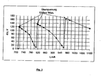
- the Indian FIG. 3 shows the course of the voltage overshoot relative to the current shows the dependence of the voltage overshoot of I0 at a constant L and the total capacity C1-3.
- L and C1-3 can be adapted to the desired lamp.
Landscapes
- Circuit Arrangements For Discharge Lamps (AREA)
Claims (18)
- Ballast électronique pour opérer au moins une lampe (LP), notamment conçue comme une lampe à décharge haute pression, comprenant un convertisseur incluant au moins un élément de commutation (S1, S2), convertisseur qui est susceptible de générer, par des modes commutés alternantes de l'au moins un élément de commutation (S1, S2), une tension avec une polarité alternante à la lampe (LP), et de fournir une puissance de fonctionnement continu, et convertisseur qui comporte au moins un élément inductif (L1) et au moins un élément capacitif (C1, C2, C3) aptes à fournir une tension de transfert supérieure à la tension appliquée pendent le fonctionnement continu, au moins après l'allumage de la lampe (LP) par un dispositif d'allumage (G1), caractérisé en ce que le ballast est conçu de sorte que la tension produite à la lampe (LP) pendent un mode commuté initial et présentant une première polarité est réduite pendent le mode commuté ultérieure par la commutation de l'élément de commutation (S1, S2), ladite tension étant réduite jusqu'à l'obtention d'une tension réduite qui correspond à une surélévation de tension (Uüber) demandée et avec l'élément de commutation destiné à la génération de la tension de transfert restant à l'état interconnecté et, en cas d'un changement de polarité, provoquant à force de l'état commuté constant de l'élément de commutation (S1, S2) un transfert de l'énergie accumulé dans l'élément capacitif (C1, C2, C3) vers l'élément inductif (L1), et une surélévation de tension (Uüber) étant produite à force de cet énergie et sous l'évitement d'une résonance à travers de l'élément capacitif (C1, C2, C3), pour mettre une tension de transfert à disposition à la lampe.
- Ballast électronique selon la revendication 1, caractérisé en ce qu'au moins une partie de l'énergie accumulé pendent un premier mode commuté dans l'élément capacitif (C1, C2, C3) pour fournir une puissance de fonctionnement continue est destinée à la production de la tension de transfert pendent le mode commuté ultérieur.
- Ballast électronique selon les revendications 1 ou 2, caractérisé en ce que, pour l'état de commutation constant de l'élément de commutation (S1, S2), le convertisseur présente la condition que le courant (I1) au travers de l'élément inductif soit inférieur à une valeur nominale prédéterminée 10.
- Ballast électronique selon la revendication 3, caractérisé en ce que le convertisseur est conçu de sorte que Uüber < 10 * (L/C)^(1/2) s'applique à la proportion surélévée Uüber de la tension de transfert, L étant l'inductance de l'élément inductif (L1) et C étant la capacité de l'élément capacitif (C1, C2, C3).
- Ballast électronique selon l'une des revendications précédentes, dans lequel le convertisseur comporte deux éléments de commutation (S1, S2), caractérisé en ce que le premier élément de commutation (S1) est prévu pour le premier mode commuté et/ou le mode commuté initial et le deuxième élément de commutation (S2) est prévu pour le deuxième mode commuté et/ou le mode commuté ultérieur.
- Ballast électronique selon la revendication 5, caractérisé en ce que les deux éléments de commutation (S1, S2) font partie d'un montage demi-pont pour l'opération de la lampe.
- Ballast électronique selon l'une des revendications précédentes, caractérisé par un dispositif d'allumage additionnel (01) intégré dans le ballast.
- Ballast électronique selon la revendication 7, caractérisé en ce que le dispositif d'allumage (G1) présente au moins une partie de la capacité de l'élément capacitif (C1, C2, C3).
- Ballast électronique selon l'une des revendications précédentes, caractérisé en ce que le convertisseur comporte au moins une bobine primaire qui est couplée avec une diode en série avec l'élément inductif (L1) pour détecter le courant de la lampe précisément suivant la forme, phase et/ou amplitude dans un circuit secondaire qui doit être alloué à un dispositif de mesure du courant.
- Ballast électronique selon la revendication 9, caractérisé en ce que les bobines primaires sont connectées de manière sérielle par rapport à l'élément inductif (L1) d'une manière découplée par une diode respective allouée aux bobines primaires.
- Appareil d'éclairage avec une lampe (LP) conçue de préférence comme une lampe de décharge haute pression, caractérisé par un ballast électronique selon l'une des revendications précédentes.
- Procédé pour l'opération d'un ballast électronique pour au moins une lampe (LP) notamment conçue comme une lampe de décharge haute pression, comprenant un convertisseur présentant au moins un élément de commutation (St S2), convertisseur qui est susceptible de générer, par des modes commutés alternants de l'au moins un élément de commutation (S1, S2), une tension avec une polarité alternante à la lampe (LP), et de fournir une puissance de fonctionnement continu, et convertisseur qui comporte au moins un élément inductif (L1) et au moins un élément capacitif (C) aptes à fournir une tension de transfert supérieure à la tension appliquée pendent le fonctionnement continu, au moins après l'allumage de la lampe (LP) par un dispositif d'allumage (G), ledit ballast étant conçu notamment selon l'une des revendications 1 à 11, caractérisé en ce que la tension produite à la lampe (LP) pendent un mode commuté initial et présentant une première polarité est réduite pendent le mode commuté ultérieur par la commutation de l'élément de commutation (S1, S2) jusqu'à l'obtention d'une tension réduite qui corresponde à une surélévation de tension (Uüber) demandée et avec l'élément de commutation destiné à la génération de la tension de transfert restant à l'état interconnecté et, en cas d'un changement de polarité, provoquant à force de l'état constant de commutation de l'élément de commutation (S1, S2) un transfert de l'énergie accumulé dans l'élément capacitif vers l'élément inductif (L1), et une surélévation de tension étant produite à force de cet énergie et sous l'évitement d'une résonance à travers de l'élément capacitif (C1, C2, C3), pour mettre une tension de transfert à disposition à la lampe.
- Procédé selon la revendication 12, caractérisé en ce que l'élément de commutation (S1, S2) est interconnecté à l'état de commutation constant.
- Procédé selon la revendication 12 ou 13, caractérisé en ce que la condition Uüber < 10 * (L/C)^(1/2) est remplie pour la proportion surélévée Uüber de la tension de transfert, dans laquelle 10 est une valeur limite du courant s'écoulant au travers de l'élément inductif.
- Procédé selon l'une des revendications 12 à 14, dans lequel le convertisseur comporte deux éléments de commutation (S1, S2), caractérisé en ce que, pour fournir la puissance de fonctionnement continu, le premier élément de commutation (S1) est opéré pendent un premier et le deuxième élément de commutation (S1, S2) pendent un deuxième mode commuté.
- Procédé selon la revendication 15, caractérisé en ce que les deux éléments de commutation (S1, S2) sont opérés comme une partie d'un montage en demi-pont.
- Procédé selon l'une des revendications 15 ou 16, caractérisé en ce que le deuxième élément de commutation (S2, S1) est coupé de nouveau après la génération de la tension de transfert lorsque le courant à travers de l'élément inductif (L1) est environ zéro.
- Procédé pour opérer un appareil d'éclairage selon la revendication 11, caractérisé en ce que le ballast électronique de l'appareil d'éclairage est opéré suivant un procédé selon l'une des revendications 12 à 17.
Applications Claiming Priority (1)
| Application Number | Priority Date | Filing Date | Title |
|---|---|---|---|
| DE200810014996 DE102008014996A1 (de) | 2008-03-19 | 2008-03-19 | Elektronisches Vorschaltgerät, Beleuchtungsgerät und Verfahren zum Betrieb dieser |
Publications (2)
| Publication Number | Publication Date |
|---|---|
| EP2104403A1 EP2104403A1 (fr) | 2009-09-23 |
| EP2104403B1 true EP2104403B1 (fr) | 2013-10-09 |
Family
ID=40834427
Family Applications (1)
| Application Number | Title | Priority Date | Filing Date |
|---|---|---|---|
| EP20090003869 Not-in-force EP2104403B1 (fr) | 2008-03-19 | 2009-03-18 | Ballast électronique, appareil d'éclairage et son procédé de fonctionnement |
Country Status (2)
| Country | Link |
|---|---|
| EP (1) | EP2104403B1 (fr) |
| DE (1) | DE102008014996A1 (fr) |
Families Citing this family (1)
| Publication number | Priority date | Publication date | Assignee | Title |
|---|---|---|---|---|
| DE102010040449A1 (de) * | 2010-09-09 | 2012-03-15 | Osram Ag | Schaltungsanordnung und Verfahren zum Starten und Betreiben einer Hochdruckentladungslampe |
Family Cites Families (6)
| Publication number | Priority date | Publication date | Assignee | Title |
|---|---|---|---|---|
| US4734624A (en) * | 1985-07-25 | 1988-03-29 | Matsushita Electric Works, Ltd. | Discharge lamp driving circuit |
| US5677602A (en) | 1995-05-26 | 1997-10-14 | Paul; Jon D. | High efficiency electronic ballast for high intensity discharge lamps |
| DE19916878B4 (de) * | 1998-09-18 | 2011-06-22 | Tridonic Ag | Schaltungsanordnung und Verfahren zum Betreiben von Gasentladungslampen |
| US6380694B1 (en) | 2000-09-22 | 2002-04-30 | Matsushita Electric Works R & D Laboratory | Variable structure circuit topology for HID lamp electronic ballasts |
| JP4087292B2 (ja) * | 2003-05-26 | 2008-05-21 | 三菱電機株式会社 | 高輝度放電ランプ点灯装置およびその点灯方法 |
| DE102005023171A1 (de) * | 2004-05-28 | 2005-12-22 | Harison Toshiba Lighting Corp. | Lichtvorrichtung für Entladungslampen |
-
2008
- 2008-03-19 DE DE200810014996 patent/DE102008014996A1/de not_active Ceased
-
2009
- 2009-03-18 EP EP20090003869 patent/EP2104403B1/fr not_active Not-in-force
Also Published As
| Publication number | Publication date |
|---|---|
| EP2104403A1 (fr) | 2009-09-23 |
| DE102008014996A1 (de) | 2009-09-24 |
Similar Documents
| Publication | Publication Date | Title |
|---|---|---|
| DE10025610B4 (de) | Ansteuergerät für eine Entladungslampe | |
| DE3715162C2 (fr) | ||
| DE19531966C2 (de) | Stromversorgungsschaltung für eine Hochdruck-Entladungslampe | |
| DE69621889T2 (de) | Anordnung zum Betreiben einer Kaltkathodenlampe mit einem piezoelektrischen Wandler | |
| DE19606874A1 (de) | Stromversorgungsvorrichtung | |
| DE102007040383A1 (de) | Entladungslampen-Zündschaltung | |
| EP2140731A2 (fr) | Circuiterie pour l'allumage et l'utilisation d'une lampe à décharge | |
| DE102007062242A1 (de) | Entladungslampe-Erregungsschaltung | |
| EP1202612B1 (fr) | Dispositif d'éclairage à préchauffage amélioré pour lampes à décharge | |
| DE10200004A1 (de) | Elektronische Schaltung und Verfahren zum Betreiben einer Hochdrucklampe | |
| DE60223971T2 (de) | Vorschaltgerät für eine Entladungslampe | |
| DE112006001948T5 (de) | DC/DC-Umrichtervorrichtung und Entladelampen-Leuchtvorrichtung | |
| DE102006023185A1 (de) | Entladungslampen-Lichtstromkreis | |
| DE102018129567A1 (de) | Leistungswandler | |
| DE69807118T2 (de) | Vorschaltgerät für eine gasentlampe | |
| DE10030176A1 (de) | Entladungslampen-Lichtstromkreis | |
| WO2002090767A1 (fr) | Systeme d'allumage pour moteurs a combustion interne | |
| WO2010139528A9 (fr) | Agencement de circuits pour un piézotransformateur, ainsi que procédé correspondant | |
| EP2104403B1 (fr) | Ballast électronique, appareil d'éclairage et son procédé de fonctionnement | |
| DE102017221786A1 (de) | Lampenbetriebsgerät mit Konverter im DCM | |
| EP1585372B1 (fr) | Ballast électronique avec exitation par résonance se chargeant de la génération de tension | |
| EP2274960B1 (fr) | Procédé et agencement de circuits pour faire fonctionner au moins une lampe à décharge | |
| EP1385358A1 (fr) | Circuit d'amorçage pour une lampe HID | |
| EP2796012B1 (fr) | Procédé, appareillage d'alimentation et système d'éclairage, avec détection d'effet de redressement de lampes | |
| EP1583403B1 (fr) | Ballast pour au moins une lampe |
Legal Events
| Date | Code | Title | Description |
|---|---|---|---|
| PUAI | Public reference made under article 153(3) epc to a published international application that has entered the european phase |
Free format text: ORIGINAL CODE: 0009012 |
|
| AK | Designated contracting states |
Kind code of ref document: A1 Designated state(s): AT BE BG CH CY CZ DE DK EE ES FI FR GB GR HR HU IE IS IT LI LT LU LV MC MK MT NL NO PL PT RO SE SI SK TR |
|
| AX | Request for extension of the european patent |
Extension state: AL BA RS |
|
| 17P | Request for examination filed |
Effective date: 20100318 |
|
| AKX | Designation fees paid |
Designated state(s): AT BE BG CH CY CZ DE DK EE ES FI FR GB GR HR HU IE IS IT LI LT LU LV MC MK MT NL NO PL PT RO SE SI SK TR |
|
| RAP1 | Party data changed (applicant data changed or rights of an application transferred) |
Owner name: BAG ENGINEERING GMBH |
|
| 17Q | First examination report despatched |
Effective date: 20110909 |
|
| RAP1 | Party data changed (applicant data changed or rights of an application transferred) |
Owner name: BAG ENGINEERING GMBH |
|
| GRAP | Despatch of communication of intention to grant a patent |
Free format text: ORIGINAL CODE: EPIDOSNIGR1 |
|
| INTG | Intention to grant announced |
Effective date: 20130606 |
|
| RIN1 | Information on inventor provided before grant (corrected) |
Inventor name: MEYER, OTTO Inventor name: WIEBE, DR. PETER |
|
| GRAS | Grant fee paid |
Free format text: ORIGINAL CODE: EPIDOSNIGR3 |
|
| GRAA | (expected) grant |
Free format text: ORIGINAL CODE: 0009210 |
|
| AK | Designated contracting states |
Kind code of ref document: B1 Designated state(s): AT BE BG CH CY CZ DE DK EE ES FI FR GB GR HR HU IE IS IT LI LT LU LV MC MK MT NL NO PL PT RO SE SI SK TR |
|
| REG | Reference to a national code |
Ref country code: GB Ref legal event code: FG4D Free format text: NOT ENGLISH |
|
| REG | Reference to a national code |
Ref country code: AT Ref legal event code: REF Ref document number: 635990 Country of ref document: AT Kind code of ref document: T Effective date: 20131015 Ref country code: CH Ref legal event code: EP |
|
| REG | Reference to a national code |
Ref country code: IE Ref legal event code: FG4D Free format text: LANGUAGE OF EP DOCUMENT: GERMAN |
|
| REG | Reference to a national code |
Ref country code: DE Ref legal event code: R096 Ref document number: 502009008117 Country of ref document: DE Effective date: 20131205 |
|
| REG | Reference to a national code |
Ref country code: NL Ref legal event code: VDEP Effective date: 20131009 |
|
| PG25 | Lapsed in a contracting state [announced via postgrant information from national office to epo] |
Ref country code: SI Free format text: LAPSE BECAUSE OF FAILURE TO SUBMIT A TRANSLATION OF THE DESCRIPTION OR TO PAY THE FEE WITHIN THE PRESCRIBED TIME-LIMIT Effective date: 20131009 |
|
| REG | Reference to a national code |
Ref country code: LT Ref legal event code: MG4D |
|
| PG25 | Lapsed in a contracting state [announced via postgrant information from national office to epo] |
Ref country code: FI Free format text: LAPSE BECAUSE OF FAILURE TO SUBMIT A TRANSLATION OF THE DESCRIPTION OR TO PAY THE FEE WITHIN THE PRESCRIBED TIME-LIMIT Effective date: 20131009 Ref country code: NO Free format text: LAPSE BECAUSE OF FAILURE TO SUBMIT A TRANSLATION OF THE DESCRIPTION OR TO PAY THE FEE WITHIN THE PRESCRIBED TIME-LIMIT Effective date: 20140109 Ref country code: LT Free format text: LAPSE BECAUSE OF FAILURE TO SUBMIT A TRANSLATION OF THE DESCRIPTION OR TO PAY THE FEE WITHIN THE PRESCRIBED TIME-LIMIT Effective date: 20131009 Ref country code: SE Free format text: LAPSE BECAUSE OF FAILURE TO SUBMIT A TRANSLATION OF THE DESCRIPTION OR TO PAY THE FEE WITHIN THE PRESCRIBED TIME-LIMIT Effective date: 20131009 Ref country code: IS Free format text: LAPSE BECAUSE OF FAILURE TO SUBMIT A TRANSLATION OF THE DESCRIPTION OR TO PAY THE FEE WITHIN THE PRESCRIBED TIME-LIMIT Effective date: 20140209 Ref country code: NL Free format text: LAPSE BECAUSE OF FAILURE TO SUBMIT A TRANSLATION OF THE DESCRIPTION OR TO PAY THE FEE WITHIN THE PRESCRIBED TIME-LIMIT Effective date: 20131009 Ref country code: HR Free format text: LAPSE BECAUSE OF FAILURE TO SUBMIT A TRANSLATION OF THE DESCRIPTION OR TO PAY THE FEE WITHIN THE PRESCRIBED TIME-LIMIT Effective date: 20131009 |
|
| PG25 | Lapsed in a contracting state [announced via postgrant information from national office to epo] |
Ref country code: LV Free format text: LAPSE BECAUSE OF FAILURE TO SUBMIT A TRANSLATION OF THE DESCRIPTION OR TO PAY THE FEE WITHIN THE PRESCRIBED TIME-LIMIT Effective date: 20131009 Ref country code: CY Free format text: LAPSE BECAUSE OF FAILURE TO SUBMIT A TRANSLATION OF THE DESCRIPTION OR TO PAY THE FEE WITHIN THE PRESCRIBED TIME-LIMIT Effective date: 20131009 Ref country code: ES Free format text: LAPSE BECAUSE OF FAILURE TO SUBMIT A TRANSLATION OF THE DESCRIPTION OR TO PAY THE FEE WITHIN THE PRESCRIBED TIME-LIMIT Effective date: 20131009 Ref country code: PL Free format text: LAPSE BECAUSE OF FAILURE TO SUBMIT A TRANSLATION OF THE DESCRIPTION OR TO PAY THE FEE WITHIN THE PRESCRIBED TIME-LIMIT Effective date: 20131009 |
|
| PG25 | Lapsed in a contracting state [announced via postgrant information from national office to epo] |
Ref country code: PT Free format text: LAPSE BECAUSE OF FAILURE TO SUBMIT A TRANSLATION OF THE DESCRIPTION OR TO PAY THE FEE WITHIN THE PRESCRIBED TIME-LIMIT Effective date: 20140210 |
|
| REG | Reference to a national code |
Ref country code: DE Ref legal event code: R097 Ref document number: 502009008117 Country of ref document: DE |
|
| PG25 | Lapsed in a contracting state [announced via postgrant information from national office to epo] |
Ref country code: EE Free format text: LAPSE BECAUSE OF FAILURE TO SUBMIT A TRANSLATION OF THE DESCRIPTION OR TO PAY THE FEE WITHIN THE PRESCRIBED TIME-LIMIT Effective date: 20131009 |
|
| PLBE | No opposition filed within time limit |
Free format text: ORIGINAL CODE: 0009261 |
|
| STAA | Information on the status of an ep patent application or granted ep patent |
Free format text: STATUS: NO OPPOSITION FILED WITHIN TIME LIMIT |
|
| PG25 | Lapsed in a contracting state [announced via postgrant information from national office to epo] |
Ref country code: IT Free format text: LAPSE BECAUSE OF FAILURE TO SUBMIT A TRANSLATION OF THE DESCRIPTION OR TO PAY THE FEE WITHIN THE PRESCRIBED TIME-LIMIT Effective date: 20131009 Ref country code: CZ Free format text: LAPSE BECAUSE OF FAILURE TO SUBMIT A TRANSLATION OF THE DESCRIPTION OR TO PAY THE FEE WITHIN THE PRESCRIBED TIME-LIMIT Effective date: 20131009 Ref country code: SK Free format text: LAPSE BECAUSE OF FAILURE TO SUBMIT A TRANSLATION OF THE DESCRIPTION OR TO PAY THE FEE WITHIN THE PRESCRIBED TIME-LIMIT Effective date: 20131009 Ref country code: RO Free format text: LAPSE BECAUSE OF FAILURE TO SUBMIT A TRANSLATION OF THE DESCRIPTION OR TO PAY THE FEE WITHIN THE PRESCRIBED TIME-LIMIT Effective date: 20131009 |
|
| 26N | No opposition filed |
Effective date: 20140710 |
|
| PG25 | Lapsed in a contracting state [announced via postgrant information from national office to epo] |
Ref country code: DK Free format text: LAPSE BECAUSE OF FAILURE TO SUBMIT A TRANSLATION OF THE DESCRIPTION OR TO PAY THE FEE WITHIN THE PRESCRIBED TIME-LIMIT Effective date: 20131009 |
|
| REG | Reference to a national code |
Ref country code: DE Ref legal event code: R097 Ref document number: 502009008117 Country of ref document: DE Effective date: 20140710 |
|
| PG25 | Lapsed in a contracting state [announced via postgrant information from national office to epo] |
Ref country code: LU Free format text: LAPSE BECAUSE OF FAILURE TO SUBMIT A TRANSLATION OF THE DESCRIPTION OR TO PAY THE FEE WITHIN THE PRESCRIBED TIME-LIMIT Effective date: 20140318 |
|
| REG | Reference to a national code |
Ref country code: CH Ref legal event code: PL |
|
| REG | Reference to a national code |
Ref country code: IE Ref legal event code: MM4A |
|
| PG25 | Lapsed in a contracting state [announced via postgrant information from national office to epo] |
Ref country code: IE Free format text: LAPSE BECAUSE OF NON-PAYMENT OF DUE FEES Effective date: 20140318 Ref country code: LI Free format text: LAPSE BECAUSE OF NON-PAYMENT OF DUE FEES Effective date: 20140331 Ref country code: CH Free format text: LAPSE BECAUSE OF NON-PAYMENT OF DUE FEES Effective date: 20140331 |
|
| REG | Reference to a national code |
Ref country code: FR Ref legal event code: PLFP Year of fee payment: 7 |
|
| PGFP | Annual fee paid to national office [announced via postgrant information from national office to epo] |
Ref country code: FR Payment date: 20150319 Year of fee payment: 7 Ref country code: GB Payment date: 20150324 Year of fee payment: 7 Ref country code: AT Payment date: 20150320 Year of fee payment: 7 |
|
| PG25 | Lapsed in a contracting state [announced via postgrant information from national office to epo] |
Ref country code: MT Free format text: LAPSE BECAUSE OF FAILURE TO SUBMIT A TRANSLATION OF THE DESCRIPTION OR TO PAY THE FEE WITHIN THE PRESCRIBED TIME-LIMIT Effective date: 20131009 |
|
| PG25 | Lapsed in a contracting state [announced via postgrant information from national office to epo] |
Ref country code: MC Free format text: LAPSE BECAUSE OF FAILURE TO SUBMIT A TRANSLATION OF THE DESCRIPTION OR TO PAY THE FEE WITHIN THE PRESCRIBED TIME-LIMIT Effective date: 20131009 |
|
| PG25 | Lapsed in a contracting state [announced via postgrant information from national office to epo] |
Ref country code: GR Free format text: LAPSE BECAUSE OF FAILURE TO SUBMIT A TRANSLATION OF THE DESCRIPTION OR TO PAY THE FEE WITHIN THE PRESCRIBED TIME-LIMIT Effective date: 20140110 Ref country code: BG Free format text: LAPSE BECAUSE OF FAILURE TO SUBMIT A TRANSLATION OF THE DESCRIPTION OR TO PAY THE FEE WITHIN THE PRESCRIBED TIME-LIMIT Effective date: 20131009 |
|
| PG25 | Lapsed in a contracting state [announced via postgrant information from national office to epo] |
Ref country code: HU Free format text: LAPSE BECAUSE OF FAILURE TO SUBMIT A TRANSLATION OF THE DESCRIPTION OR TO PAY THE FEE WITHIN THE PRESCRIBED TIME-LIMIT; INVALID AB INITIO Effective date: 20090318 Ref country code: TR Free format text: LAPSE BECAUSE OF FAILURE TO SUBMIT A TRANSLATION OF THE DESCRIPTION OR TO PAY THE FEE WITHIN THE PRESCRIBED TIME-LIMIT Effective date: 20131009 Ref country code: BE Free format text: LAPSE BECAUSE OF FAILURE TO SUBMIT A TRANSLATION OF THE DESCRIPTION OR TO PAY THE FEE WITHIN THE PRESCRIBED TIME-LIMIT Effective date: 20140331 |
|
| REG | Reference to a national code |
Ref country code: DE Ref legal event code: R082 Ref document number: 502009008117 Country of ref document: DE Representative=s name: PATENTANWAELTE LIPPERT, STACHOW & PARTNER, DE Ref country code: DE Ref legal event code: R081 Ref document number: 502009008117 Country of ref document: DE Owner name: BAG ELECTRONICS GMBH, DE Free format text: FORMER OWNER: BAG ENGINEERING GMBH, 59759 ARNSBERG, DE Ref country code: DE Ref legal event code: R082 Ref document number: 502009008117 Country of ref document: DE Representative=s name: LIPPERT STACHOW PATENTANWAELTE RECHTSANWAELTE , DE |
|
| REG | Reference to a national code |
Ref country code: AT Ref legal event code: MM01 Ref document number: 635990 Country of ref document: AT Kind code of ref document: T Effective date: 20160318 |
|
| GBPC | Gb: european patent ceased through non-payment of renewal fee |
Effective date: 20160318 |
|
| REG | Reference to a national code |
Ref country code: FR Ref legal event code: ST Effective date: 20161130 |
|
| PG25 | Lapsed in a contracting state [announced via postgrant information from national office to epo] |
Ref country code: FR Free format text: LAPSE BECAUSE OF NON-PAYMENT OF DUE FEES Effective date: 20160331 Ref country code: GB Free format text: LAPSE BECAUSE OF NON-PAYMENT OF DUE FEES Effective date: 20160318 |
|
| PG25 | Lapsed in a contracting state [announced via postgrant information from national office to epo] |
Ref country code: AT Free format text: LAPSE BECAUSE OF NON-PAYMENT OF DUE FEES Effective date: 20160318 |
|
| PG25 | Lapsed in a contracting state [announced via postgrant information from national office to epo] |
Ref country code: MK Free format text: LAPSE BECAUSE OF FAILURE TO SUBMIT A TRANSLATION OF THE DESCRIPTION OR TO PAY THE FEE WITHIN THE PRESCRIBED TIME-LIMIT Effective date: 20131009 |
|
| PGFP | Annual fee paid to national office [announced via postgrant information from national office to epo] |
Ref country code: DE Payment date: 20180528 Year of fee payment: 10 |
|
| REG | Reference to a national code |
Ref country code: DE Ref legal event code: R119 Ref document number: 502009008117 Country of ref document: DE |
|
| PG25 | Lapsed in a contracting state [announced via postgrant information from national office to epo] |
Ref country code: DE Free format text: LAPSE BECAUSE OF NON-PAYMENT OF DUE FEES Effective date: 20191001 |