EP2092807B1 - Matières d'encapsulation organiques composites - Google Patents
Matières d'encapsulation organiques composites Download PDFInfo
- Publication number
- EP2092807B1 EP2092807B1 EP07862748.6A EP07862748A EP2092807B1 EP 2092807 B1 EP2092807 B1 EP 2092807B1 EP 07862748 A EP07862748 A EP 07862748A EP 2092807 B1 EP2092807 B1 EP 2092807B1
- Authority
- EP
- European Patent Office
- Prior art keywords
- bis
- encapsulant
- layer
- dianhydride
- epoxy
- Prior art date
- Legal status (The legal status is an assumption and is not a legal conclusion. Google has not performed a legal analysis and makes no representation as to the accuracy of the status listed.)
- Active
Links
- 239000008393 encapsulating agent Substances 0.000 title claims description 117
- 239000002131 composite material Substances 0.000 title description 11
- 239000000203 mixture Substances 0.000 claims description 84
- 229920001721 polyimide Polymers 0.000 claims description 34
- 239000004593 Epoxy Substances 0.000 claims description 31
- 239000011888 foil Substances 0.000 claims description 29
- 239000004642 Polyimide Substances 0.000 claims description 28
- 238000010521 absorption reaction Methods 0.000 claims description 26
- XLYOFNOQVPJJNP-UHFFFAOYSA-N water Substances O XLYOFNOQVPJJNP-UHFFFAOYSA-N 0.000 claims description 26
- GTDPSWPPOUPBNX-UHFFFAOYSA-N ac1mqpva Chemical compound CC12C(=O)OC(=O)C1(C)C1(C)C2(C)C(=O)OC1=O GTDPSWPPOUPBNX-UHFFFAOYSA-N 0.000 claims description 24
- 229920000642 polymer Polymers 0.000 claims description 24
- 150000004985 diamines Chemical class 0.000 claims description 19
- -1 3-amino-4-hydroxyphenyl Chemical group 0.000 claims description 18
- 229920001568 phenolic resin Polymers 0.000 claims description 17
- 239000005011 phenolic resin Substances 0.000 claims description 17
- 239000003985 ceramic capacitor Substances 0.000 claims description 15
- 239000003960 organic solvent Substances 0.000 claims description 15
- 239000000126 substance Substances 0.000 claims description 14
- 239000003054 catalyst Substances 0.000 claims description 13
- 125000004122 cyclic group Chemical group 0.000 claims description 12
- KXGFMDJXCMQABM-UHFFFAOYSA-N 2-methoxy-6-methylphenol Chemical compound [CH]OC1=CC=CC([CH])=C1O KXGFMDJXCMQABM-UHFFFAOYSA-N 0.000 claims description 11
- 239000003086 colorant Substances 0.000 claims description 11
- 239000000945 filler Substances 0.000 claims description 11
- ISWSIDIOOBJBQZ-UHFFFAOYSA-N phenol group Chemical group C1(=CC=CC=C1)O ISWSIDIOOBJBQZ-UHFFFAOYSA-N 0.000 claims description 11
- 229920005672 polyolefin resin Polymers 0.000 claims description 11
- 239000013530 defoamer Substances 0.000 claims description 7
- HECLRDQVFMWTQS-RGOKHQFPSA-N 1755-01-7 Chemical compound C1[C@H]2[C@@H]3CC=C[C@@H]3[C@@H]1C=C2 HECLRDQVFMWTQS-RGOKHQFPSA-N 0.000 claims description 6
- NVKGJHAQGWCWDI-UHFFFAOYSA-N 4-[4-amino-2-(trifluoromethyl)phenyl]-3-(trifluoromethyl)aniline Chemical group FC(F)(F)C1=CC(N)=CC=C1C1=CC=C(N)C=C1C(F)(F)F NVKGJHAQGWCWDI-UHFFFAOYSA-N 0.000 claims description 6
- ZHBXLZQQVCDGPA-UHFFFAOYSA-N 5-[(1,3-dioxo-2-benzofuran-5-yl)sulfonyl]-2-benzofuran-1,3-dione Chemical compound C1=C2C(=O)OC(=O)C2=CC(S(=O)(=O)C=2C=C3C(=O)OC(C3=CC=2)=O)=C1 ZHBXLZQQVCDGPA-UHFFFAOYSA-N 0.000 claims description 6
- 239000011248 coating agent Substances 0.000 claims description 6
- 238000000576 coating method Methods 0.000 claims description 6
- 239000003822 epoxy resin Substances 0.000 claims description 5
- 229920000647 polyepoxide Polymers 0.000 claims description 5
- UAIUNKRWKOVEES-UHFFFAOYSA-N 3,3',5,5'-tetramethylbenzidine Chemical compound CC1=C(N)C(C)=CC(C=2C=C(C)C(N)=C(C)C=2)=C1 UAIUNKRWKOVEES-UHFFFAOYSA-N 0.000 claims description 4
- QQGYZOYWNCKGEK-UHFFFAOYSA-N 5-[(1,3-dioxo-2-benzofuran-5-yl)oxy]-2-benzofuran-1,3-dione Chemical compound C1=C2C(=O)OC(=O)C2=CC(OC=2C=C3C(=O)OC(C3=CC=2)=O)=C1 QQGYZOYWNCKGEK-UHFFFAOYSA-N 0.000 claims description 4
- ATUOYWHBWRKTHZ-UHFFFAOYSA-N Propane Chemical compound CCC ATUOYWHBWRKTHZ-UHFFFAOYSA-N 0.000 claims description 4
- VNWKTOKETHGBQD-UHFFFAOYSA-N methane Chemical compound C VNWKTOKETHGBQD-UHFFFAOYSA-N 0.000 claims description 4
- 125000001997 phenyl group Chemical group [H]C1=C([H])C([H])=C(*)C([H])=C1[H] 0.000 claims description 4
- NSGXIBWMJZWTPY-UHFFFAOYSA-N 1,1,1,3,3,3-hexafluoropropane Chemical compound FC(F)(F)CC(F)(F)F NSGXIBWMJZWTPY-UHFFFAOYSA-N 0.000 claims description 3
- ZGDMDBHLKNQPSD-UHFFFAOYSA-N 2-amino-5-(4-amino-3-hydroxyphenyl)phenol Chemical group C1=C(O)C(N)=CC=C1C1=CC=C(N)C(O)=C1 ZGDMDBHLKNQPSD-UHFFFAOYSA-N 0.000 claims description 3
- PJWQLRKRVISYPL-UHFFFAOYSA-N 4-[4-amino-3-(trifluoromethyl)phenyl]-2-(trifluoromethyl)aniline Chemical compound C1=C(C(F)(F)F)C(N)=CC=C1C1=CC=C(N)C(C(F)(F)F)=C1 PJWQLRKRVISYPL-UHFFFAOYSA-N 0.000 claims description 3
- 125000003700 epoxy group Chemical group 0.000 claims description 3
- 125000000008 (C1-C10) alkyl group Chemical group 0.000 claims description 2
- XDGSIIBFQCVQPU-UHFFFAOYSA-N 1-(1,1,2,2,2-pentafluoroethyl)cyclohexa-3,5-diene-1,3-diamine Chemical compound NC1=CC=CC(N)(C(F)(F)C(F)(F)F)C1 XDGSIIBFQCVQPU-UHFFFAOYSA-N 0.000 claims description 2
- BBHKJYQVKZWEDW-UHFFFAOYSA-N 1-(1,1,2,2,3,3,3-heptafluoropropyl)cyclohexa-3,5-diene-1,3-diamine Chemical compound NC1=CC=CC(N)(C(F)(F)C(F)(F)C(F)(F)F)C1 BBHKJYQVKZWEDW-UHFFFAOYSA-N 0.000 claims description 2
- QZAQJDMAOKERBY-UHFFFAOYSA-N 12,12-bis(trifluoromethyl)-2,7,17-trioxapentacyclo[11.7.0.03,11.05,9.015,19]icosa-1(13),3(11),4,9,14,19-hexaene-6,8,16,18-tetrone Chemical compound C1=C2OC3=CC=4C(=O)OC(=O)C=4C=C3C(C(F)(F)F)(C(F)(F)F)C2=CC2=C1C(=O)OC2=O QZAQJDMAOKERBY-UHFFFAOYSA-N 0.000 claims description 2
- WCZNKVPCIFMXEQ-UHFFFAOYSA-N 2,3,5,6-tetramethylbenzene-1,4-diamine Chemical compound CC1=C(C)C(N)=C(C)C(C)=C1N WCZNKVPCIFMXEQ-UHFFFAOYSA-N 0.000 claims description 2
- PCAXITAPTVOLGL-UHFFFAOYSA-N 2,3-diaminophenol Chemical compound NC1=CC=CC(O)=C1N PCAXITAPTVOLGL-UHFFFAOYSA-N 0.000 claims description 2
- CEQNIRIQYOUDCF-UHFFFAOYSA-N 2,5-bis(trifluoromethyl)benzene-1,4-diamine Chemical compound NC1=CC(C(F)(F)F)=C(N)C=C1C(F)(F)F CEQNIRIQYOUDCF-UHFFFAOYSA-N 0.000 claims description 2
- KZLDGFZCFRXUIB-UHFFFAOYSA-N 2-amino-4-(3-amino-4-hydroxyphenyl)phenol Chemical group C1=C(O)C(N)=CC(C=2C=C(N)C(O)=CC=2)=C1 KZLDGFZCFRXUIB-UHFFFAOYSA-N 0.000 claims description 2
- NUIURNJTPRWVAP-UHFFFAOYSA-N 3,3'-Dimethylbenzidine Chemical compound C1=C(N)C(C)=CC(C=2C=C(C)C(N)=CC=2)=C1 NUIURNJTPRWVAP-UHFFFAOYSA-N 0.000 claims description 2
- LJGHYPLBDBRCRZ-UHFFFAOYSA-N 3-(3-aminophenyl)sulfonylaniline Chemical compound NC1=CC=CC(S(=O)(=O)C=2C=C(N)C=CC=2)=C1 LJGHYPLBDBRCRZ-UHFFFAOYSA-N 0.000 claims description 2
- ZBMISJGHVWNWTE-UHFFFAOYSA-N 3-(4-aminophenoxy)aniline Chemical compound C1=CC(N)=CC=C1OC1=CC=CC(N)=C1 ZBMISJGHVWNWTE-UHFFFAOYSA-N 0.000 claims description 2
- UVUCUHVQYAPMEU-UHFFFAOYSA-N 3-[2-(3-aminophenyl)-1,1,1,3,3,3-hexafluoropropan-2-yl]aniline Chemical compound NC1=CC=CC(C(C=2C=C(N)C=CC=2)(C(F)(F)F)C(F)(F)F)=C1 UVUCUHVQYAPMEU-UHFFFAOYSA-N 0.000 claims description 2
- XUBKCXMWPKLPPK-UHFFFAOYSA-N 4-(4-amino-2,6-dimethylphenyl)-3,5-dimethylaniline Chemical compound CC1=CC(N)=CC(C)=C1C1=C(C)C=C(N)C=C1C XUBKCXMWPKLPPK-UHFFFAOYSA-N 0.000 claims description 2
- QYIMZXITLDTULQ-UHFFFAOYSA-N 4-(4-amino-2-methylphenyl)-3-methylaniline Chemical compound CC1=CC(N)=CC=C1C1=CC=C(N)C=C1C QYIMZXITLDTULQ-UHFFFAOYSA-N 0.000 claims description 2
- PTWQVOITXCIGEB-UHFFFAOYSA-N 4-[1-(3,4-dicarboxyphenyl)-2,2,2-trifluoro-1-phenylethyl]phthalic acid Chemical compound C1=C(C(O)=O)C(C(=O)O)=CC=C1C(C(F)(F)F)(C=1C=C(C(C(O)=O)=CC=1)C(O)=O)C1=CC=CC=C1 PTWQVOITXCIGEB-UHFFFAOYSA-N 0.000 claims description 2
- GVAVRUDVIQJLPS-UHFFFAOYSA-N 4-[4-amino-2-(1,1,2,2,2-pentafluoroethoxy)phenyl]-3-(1,1,2,2,2-pentafluoroethoxy)aniline Chemical compound FC(F)(F)C(F)(F)OC1=CC(N)=CC=C1C1=CC=C(N)C=C1OC(F)(F)C(F)(F)F GVAVRUDVIQJLPS-UHFFFAOYSA-N 0.000 claims description 2
- KZSXRDLXTFEHJM-UHFFFAOYSA-N 5-(trifluoromethyl)benzene-1,3-diamine Chemical compound NC1=CC(N)=CC(C(F)(F)F)=C1 KZSXRDLXTFEHJM-UHFFFAOYSA-N 0.000 claims description 2
- QHHKLPCQTTWFSS-UHFFFAOYSA-N 5-[2-(1,3-dioxo-2-benzofuran-5-yl)-1,1,1,3,3,3-hexafluoropropan-2-yl]-2-benzofuran-1,3-dione Chemical compound C1=C2C(=O)OC(=O)C2=CC(C(C=2C=C3C(=O)OC(=O)C3=CC=2)(C(F)(F)F)C(F)(F)F)=C1 QHHKLPCQTTWFSS-UHFFFAOYSA-N 0.000 claims description 2
- HJSYPLCSZPEDCQ-UHFFFAOYSA-N 5-[2-(3-amino-4-methylphenyl)-1,1,1,3,3,3-hexafluoropropan-2-yl]-2-methylaniline Chemical compound C1=C(N)C(C)=CC=C1C(C(F)(F)F)(C(F)(F)F)C1=CC=C(C)C(N)=C1 HJSYPLCSZPEDCQ-UHFFFAOYSA-N 0.000 claims description 2
- UUBAUCGAAFFHSK-UHFFFAOYSA-N 5-[3,3,4,4,5,5,5-heptafluoro-2,2-bis(trifluoromethyl)pentyl]benzene-1,3-diamine Chemical compound NC1=CC(N)=CC(CC(C(F)(F)F)(C(F)(F)F)C(F)(F)C(F)(F)C(F)(F)F)=C1 UUBAUCGAAFFHSK-UHFFFAOYSA-N 0.000 claims description 2
- RHLWTWUMSPIQMC-UHFFFAOYSA-N 9,9-bis(trifluoromethyl)xanthene-2,3,6,7-tetracarboxylic acid Chemical compound O1C2=CC(C(O)=O)=C(C(O)=O)C=C2C(C(F)(F)F)(C(F)(F)F)C2=C1C=C(C(=O)O)C(C(O)=O)=C2 RHLWTWUMSPIQMC-UHFFFAOYSA-N 0.000 claims description 2
- RYVZWCNDGWPCKA-UHFFFAOYSA-N 9,9-bis(trifluoromethyl)xanthene-3,6-diamine Chemical compound NC1=CC=C2C(C(F)(F)F)(C(F)(F)F)C3=CC=C(N)C=C3OC2=C1 RYVZWCNDGWPCKA-UHFFFAOYSA-N 0.000 claims description 2
- VOGMUVOPUDSMOV-UHFFFAOYSA-N 9,9-dimethylxanthene-2,3,6,7-tetracarboxylic acid Chemical compound OC(=O)C1=C(C(O)=O)C=C2C(C)(C)C3=CC(C(O)=O)=C(C(O)=O)C=C3OC2=C1 VOGMUVOPUDSMOV-UHFFFAOYSA-N 0.000 claims description 2
- RIENCUFLZCDRDX-UHFFFAOYSA-N 9-methyl-9-phenylxanthene-2,3,6,7-tetracarboxylic acid Chemical compound C12=CC(C(O)=O)=C(C(O)=O)C=C2OC2=CC(C(O)=O)=C(C(O)=O)C=C2C1(C)C1=CC=CC=C1 RIENCUFLZCDRDX-UHFFFAOYSA-N 0.000 claims description 2
- VYFUAJUYFVNYHH-UHFFFAOYSA-N 9-phenyl-9-(trifluoromethyl)xanthene-2,3,6,7-tetracarboxylic acid Chemical compound C1=2C=C(C(O)=O)C(C(=O)O)=CC=2OC2=CC(C(O)=O)=C(C(O)=O)C=C2C1(C(F)(F)F)C1=CC=CC=C1 VYFUAJUYFVNYHH-UHFFFAOYSA-N 0.000 claims description 2
- UFHFLCQGNIYNRP-UHFFFAOYSA-N Hydrogen Chemical compound [H][H] UFHFLCQGNIYNRP-UHFFFAOYSA-N 0.000 claims description 2
- VZPBUASKLMWFCH-UHFFFAOYSA-N N-(trifluoromethoxy)-4-[4-(trifluoromethoxyamino)phenyl]aniline Chemical compound FC(ONC1=CC=C(C=C1)C1=CC=C(NOC(F)(F)F)C=C1)(F)F VZPBUASKLMWFCH-UHFFFAOYSA-N 0.000 claims description 2
- XIWMTQIUUWJNRP-UHFFFAOYSA-N amidol Chemical compound NC1=CC=C(O)C(N)=C1 XIWMTQIUUWJNRP-UHFFFAOYSA-N 0.000 claims description 2
- HFACYLZERDEVSX-UHFFFAOYSA-N benzidine Chemical compound C1=CC(N)=CC=C1C1=CC=C(N)C=C1 HFACYLZERDEVSX-UHFFFAOYSA-N 0.000 claims description 2
- 239000001273 butane Substances 0.000 claims description 2
- 239000001257 hydrogen Substances 0.000 claims description 2
- 229910052739 hydrogen Inorganic materials 0.000 claims description 2
- IMNDHOCGZLYMRO-UHFFFAOYSA-N n,n-dimethylbenzamide Chemical compound CN(C)C(=O)C1=CC=CC=C1 IMNDHOCGZLYMRO-UHFFFAOYSA-N 0.000 claims description 2
- IJDNQMDRQITEOD-UHFFFAOYSA-N n-butane Chemical compound CCCC IJDNQMDRQITEOD-UHFFFAOYSA-N 0.000 claims description 2
- OFBQJSOFQDEBGM-UHFFFAOYSA-N n-pentane Natural products CCCCC OFBQJSOFQDEBGM-UHFFFAOYSA-N 0.000 claims description 2
- 125000006340 pentafluoro ethyl group Chemical group FC(F)(F)C(F)(F)* 0.000 claims description 2
- 239000001294 propane Substances 0.000 claims description 2
- SUHCURMYDMVREV-UHFFFAOYSA-N 9-phenyl-9-(trifluoromethyl)xanthene-3,6-diamine Chemical compound C=1C(N)=CC=C2C=1OC1=CC(N)=CC=C1C2(C(F)(F)F)C1=CC=CC=C1 SUHCURMYDMVREV-UHFFFAOYSA-N 0.000 claims 1
- 230000009477 glass transition Effects 0.000 claims 1
- 239000003990 capacitor Substances 0.000 description 64
- 239000010408 film Substances 0.000 description 34
- RYGMFSIKBFXOCR-UHFFFAOYSA-N Copper Chemical compound [Cu] RYGMFSIKBFXOCR-UHFFFAOYSA-N 0.000 description 23
- 238000000034 method Methods 0.000 description 20
- 238000012360 testing method Methods 0.000 description 20
- 239000010949 copper Substances 0.000 description 16
- 229910052802 copper Inorganic materials 0.000 description 15
- 239000002904 solvent Substances 0.000 description 15
- IJGRMHOSHXDMSA-UHFFFAOYSA-N Atomic nitrogen Chemical compound N#N IJGRMHOSHXDMSA-UHFFFAOYSA-N 0.000 description 14
- VYPSYNLAJGMNEJ-UHFFFAOYSA-N Silicium dioxide Chemical compound O=[Si]=O VYPSYNLAJGMNEJ-UHFFFAOYSA-N 0.000 description 12
- 238000010438 heat treatment Methods 0.000 description 11
- 238000002360 preparation method Methods 0.000 description 11
- WUOACPNHFRMFPN-UHFFFAOYSA-N alpha-terpineol Chemical compound CC1=CCC(C(C)(C)O)CC1 WUOACPNHFRMFPN-UHFFFAOYSA-N 0.000 description 10
- SQIFACVGCPWBQZ-UHFFFAOYSA-N delta-terpineol Natural products CC(C)(O)C1CCC(=C)CC1 SQIFACVGCPWBQZ-UHFFFAOYSA-N 0.000 description 10
- 238000009413 insulation Methods 0.000 description 10
- 235000013824 polyphenols Nutrition 0.000 description 10
- 229920005989 resin Polymers 0.000 description 10
- 239000011347 resin Substances 0.000 description 10
- 229940116411 terpineol Drugs 0.000 description 10
- HEMHJVSKTPXQMS-UHFFFAOYSA-M Sodium hydroxide Chemical compound [OH-].[Na+] HEMHJVSKTPXQMS-UHFFFAOYSA-M 0.000 description 9
- 238000010304 firing Methods 0.000 description 9
- 239000000758 substrate Substances 0.000 description 9
- 239000007787 solid Substances 0.000 description 8
- 239000011889 copper foil Substances 0.000 description 7
- 229910052757 nitrogen Inorganic materials 0.000 description 7
- OKKJLVBELUTLKV-UHFFFAOYSA-N Methanol Chemical compound OC OKKJLVBELUTLKV-UHFFFAOYSA-N 0.000 description 6
- QAOWNCQODCNURD-UHFFFAOYSA-N Sulfuric acid Chemical compound OS(O)(=O)=O QAOWNCQODCNURD-UHFFFAOYSA-N 0.000 description 6
- 239000002253 acid Substances 0.000 description 6
- 239000003795 chemical substances by application Substances 0.000 description 6
- 239000003989 dielectric material Substances 0.000 description 6
- 239000004615 ingredient Substances 0.000 description 6
- 239000002518 antifoaming agent Substances 0.000 description 5
- 238000001723 curing Methods 0.000 description 5
- 230000032798 delamination Effects 0.000 description 5
- 238000003475 lamination Methods 0.000 description 5
- 238000011282 treatment Methods 0.000 description 5
- OKTJSMMVPCPJKN-UHFFFAOYSA-N Carbon Chemical compound [C] OKTJSMMVPCPJKN-UHFFFAOYSA-N 0.000 description 4
- PNEYBMLMFCGWSK-UHFFFAOYSA-N aluminium oxide Inorganic materials [O-2].[O-2].[O-2].[Al+3].[Al+3] PNEYBMLMFCGWSK-UHFFFAOYSA-N 0.000 description 4
- 125000006159 dianhydride group Chemical group 0.000 description 4
- UYAAVKFHBMJOJZ-UHFFFAOYSA-N diimidazo[1,3-b:1',3'-e]pyrazine-5,10-dione Chemical compound O=C1C2=CN=CN2C(=O)C2=CN=CN12 UYAAVKFHBMJOJZ-UHFFFAOYSA-N 0.000 description 4
- RTZKZFJDLAIYFH-UHFFFAOYSA-N ether Substances CCOCC RTZKZFJDLAIYFH-UHFFFAOYSA-N 0.000 description 4
- 229910021485 fumed silica Inorganic materials 0.000 description 4
- 230000002209 hydrophobic effect Effects 0.000 description 4
- 238000004519 manufacturing process Methods 0.000 description 4
- 239000000463 material Substances 0.000 description 4
- 238000002156 mixing Methods 0.000 description 4
- 125000005375 organosiloxane group Chemical group 0.000 description 4
- 239000000843 powder Substances 0.000 description 4
- 229940116423 propylene glycol diacetate Drugs 0.000 description 4
- 238000010926 purge Methods 0.000 description 4
- 239000000377 silicon dioxide Substances 0.000 description 4
- 229910000679 solder Inorganic materials 0.000 description 4
- 238000003756 stirring Methods 0.000 description 4
- QTBSBXVTEAMEQO-UHFFFAOYSA-N Acetic acid Chemical compound CC(O)=O QTBSBXVTEAMEQO-UHFFFAOYSA-N 0.000 description 3
- WFDIJRYMOXRFFG-UHFFFAOYSA-N Acetic anhydride Chemical compound CC(=O)OC(C)=O WFDIJRYMOXRFFG-UHFFFAOYSA-N 0.000 description 3
- 125000000217 alkyl group Chemical group 0.000 description 3
- QRUDEWIWKLJBPS-UHFFFAOYSA-N benzotriazole Chemical compound C1=CC=C2N[N][N]C2=C1 QRUDEWIWKLJBPS-UHFFFAOYSA-N 0.000 description 3
- 239000012964 benzotriazole Substances 0.000 description 3
- 230000015556 catabolic process Effects 0.000 description 3
- 239000000919 ceramic Substances 0.000 description 3
- 238000006731 degradation reaction Methods 0.000 description 3
- 239000011521 glass Substances 0.000 description 3
- 229920005575 poly(amic acid) Polymers 0.000 description 3
- 239000009719 polyimide resin Substances 0.000 description 3
- 238000007639 printing Methods 0.000 description 3
- 239000000047 product Substances 0.000 description 3
- 238000007650 screen-printing Methods 0.000 description 3
- YHMYGUUIMTVXNW-UHFFFAOYSA-N 1,3-dihydrobenzimidazole-2-thione Chemical compound C1=CC=C2NC(S)=NC2=C1 YHMYGUUIMTVXNW-UHFFFAOYSA-N 0.000 description 2
- ITQTTZVARXURQS-UHFFFAOYSA-N 3-methylpyridine Chemical compound CC1=CC=CN=C1 ITQTTZVARXURQS-UHFFFAOYSA-N 0.000 description 2
- LGRFSURHDFAFJT-UHFFFAOYSA-N Phthalic anhydride Natural products C1=CC=C2C(=O)OC(=O)C2=C1 LGRFSURHDFAFJT-UHFFFAOYSA-N 0.000 description 2
- 229920004482 WACKER® Polymers 0.000 description 2
- 150000001242 acetic acid derivatives Chemical class 0.000 description 2
- 239000000853 adhesive Substances 0.000 description 2
- 230000001070 adhesive effect Effects 0.000 description 2
- 230000002411 adverse Effects 0.000 description 2
- 238000013019 agitation Methods 0.000 description 2
- 150000001412 amines Chemical class 0.000 description 2
- 238000004458 analytical method Methods 0.000 description 2
- 238000013459 approach Methods 0.000 description 2
- 125000003118 aryl group Chemical group 0.000 description 2
- JHIWVOJDXOSYLW-UHFFFAOYSA-N butyl 2,2-difluorocyclopropane-1-carboxylate Chemical compound CCCCOC(=O)C1CC1(F)F JHIWVOJDXOSYLW-UHFFFAOYSA-N 0.000 description 2
- 239000003518 caustics Substances 0.000 description 2
- 238000006243 chemical reaction Methods 0.000 description 2
- 239000006184 cosolvent Substances 0.000 description 2
- 239000003431 cross linking reagent Substances 0.000 description 2
- 239000008367 deionised water Substances 0.000 description 2
- 229910021641 deionized water Inorganic materials 0.000 description 2
- 238000000151 deposition Methods 0.000 description 2
- FSCIDASGDAWVED-UHFFFAOYSA-N dimethyl hexanedioate;dimethyl pentanedioate Chemical compound COC(=O)CCCC(=O)OC.COC(=O)CCCCC(=O)OC FSCIDASGDAWVED-UHFFFAOYSA-N 0.000 description 2
- 238000004090 dissolution Methods 0.000 description 2
- 239000007772 electrode material Substances 0.000 description 2
- 238000005516 engineering process Methods 0.000 description 2
- 230000007613 environmental effect Effects 0.000 description 2
- 150000002170 ethers Chemical class 0.000 description 2
- 239000007788 liquid Substances 0.000 description 2
- 239000011159 matrix material Substances 0.000 description 2
- 239000002184 metal Substances 0.000 description 2
- 229910052751 metal Inorganic materials 0.000 description 2
- 239000012299 nitrogen atmosphere Substances 0.000 description 2
- 239000012071 phase Substances 0.000 description 2
- 229920000636 poly(norbornene) polymer Polymers 0.000 description 2
- 229920001296 polysiloxane Polymers 0.000 description 2
- 238000012545 processing Methods 0.000 description 2
- 238000000926 separation method Methods 0.000 description 2
- 239000008234 soft water Substances 0.000 description 2
- 239000011877 solvent mixture Substances 0.000 description 2
- 238000010998 test method Methods 0.000 description 2
- VXQBJTKSVGFQOL-UHFFFAOYSA-N 2-(2-butoxyethoxy)ethyl acetate Chemical compound CCCCOCCOCCOC(C)=O VXQBJTKSVGFQOL-UHFFFAOYSA-N 0.000 description 1
- FPZWZCWUIYYYBU-UHFFFAOYSA-N 2-(2-ethoxyethoxy)ethyl acetate Chemical compound CCOCCOCCOC(C)=O FPZWZCWUIYYYBU-UHFFFAOYSA-N 0.000 description 1
- APXJLYIVOFARRM-UHFFFAOYSA-N 4-[2-(3,4-dicarboxyphenyl)-1,1,1,3,3,3-hexafluoropropan-2-yl]phthalic acid Chemical compound C1=C(C(O)=O)C(C(=O)O)=CC=C1C(C(F)(F)F)(C(F)(F)F)C1=CC=C(C(O)=O)C(C(O)=O)=C1 APXJLYIVOFARRM-UHFFFAOYSA-N 0.000 description 1
- 0 CC(*)N(C(c1c2cc(*c(cc3)cc(C(N4C)=O)c3C4=O)cc1)=O)C2=O Chemical compound CC(*)N(C(c1c2cc(*c(cc3)cc(C(N4C)=O)c3C4=O)cc1)=O)C2=O 0.000 description 1
- 239000004971 Cross linker Substances 0.000 description 1
- UDSFAEKRVUSQDD-UHFFFAOYSA-N Dimethyl adipate Chemical compound COC(=O)CCCCC(=O)OC UDSFAEKRVUSQDD-UHFFFAOYSA-N 0.000 description 1
- MUXOBHXGJLMRAB-UHFFFAOYSA-N Dimethyl succinate Chemical compound COC(=O)CCC(=O)OC MUXOBHXGJLMRAB-UHFFFAOYSA-N 0.000 description 1
- 238000005481 NMR spectroscopy Methods 0.000 description 1
- MHABMANUFPZXEB-UHFFFAOYSA-N O-demethyl-aloesaponarin I Natural products O=C1C2=CC=CC(O)=C2C(=O)C2=C1C=C(O)C(C(O)=O)=C2C MHABMANUFPZXEB-UHFFFAOYSA-N 0.000 description 1
- 239000004962 Polyamide-imide Substances 0.000 description 1
- 239000004693 Polybenzimidazole Substances 0.000 description 1
- 239000004697 Polyetherimide Substances 0.000 description 1
- 239000004793 Polystyrene Substances 0.000 description 1
- OAFBETRANPRMCT-UHFFFAOYSA-N acetic acid;n,n-dimethyl-1-phenylmethanamine Chemical compound CC([O-])=O.C[NH+](C)CC1=CC=CC=C1 OAFBETRANPRMCT-UHFFFAOYSA-N 0.000 description 1
- 150000007513 acids Chemical class 0.000 description 1
- 239000000654 additive Substances 0.000 description 1
- 230000000996 additive effect Effects 0.000 description 1
- 238000005452 bending Methods 0.000 description 1
- 239000011230 binding agent Substances 0.000 description 1
- 238000009835 boiling Methods 0.000 description 1
- 125000000484 butyl group Chemical group [H]C([*])([H])C([H])([H])C([H])([H])C([H])([H])[H] 0.000 description 1
- 230000003197 catalytic effect Effects 0.000 description 1
- 239000007795 chemical reaction product Substances 0.000 description 1
- 239000008199 coating composition Substances 0.000 description 1
- 230000000052 comparative effect Effects 0.000 description 1
- 238000009833 condensation Methods 0.000 description 1
- 230000005494 condensation Effects 0.000 description 1
- 238000007596 consolidation process Methods 0.000 description 1
- 238000010276 construction Methods 0.000 description 1
- 230000007547 defect Effects 0.000 description 1
- XTDYIOOONNVFMA-UHFFFAOYSA-N dimethyl pentanedioate Chemical compound COC(=O)CCCC(=O)OC XTDYIOOONNVFMA-UHFFFAOYSA-N 0.000 description 1
- XXBDWLFCJWSEKW-UHFFFAOYSA-N dimethylbenzylamine Chemical compound CN(C)CC1=CC=CC=C1 XXBDWLFCJWSEKW-UHFFFAOYSA-N 0.000 description 1
- 239000006185 dispersion Substances 0.000 description 1
- 239000002019 doping agent Substances 0.000 description 1
- 238000011143 downstream manufacturing Methods 0.000 description 1
- 238000001035 drying Methods 0.000 description 1
- 238000005538 encapsulation Methods 0.000 description 1
- 239000003759 ester based solvent Substances 0.000 description 1
- 238000005530 etching Methods 0.000 description 1
- 125000001495 ethyl group Chemical group [H]C([H])([H])C([H])([H])* 0.000 description 1
- 238000001914 filtration Methods 0.000 description 1
- 238000009472 formulation Methods 0.000 description 1
- 230000006698 induction Effects 0.000 description 1
- 125000001449 isopropyl group Chemical group [H]C([H])([H])C([H])(*)C([H])([H])[H] 0.000 description 1
- 230000002045 lasting effect Effects 0.000 description 1
- 125000002496 methyl group Chemical group [H]C([H])([H])* 0.000 description 1
- 238000003801 milling Methods 0.000 description 1
- 239000004570 mortar (masonry) Substances 0.000 description 1
- 239000011368 organic material Substances 0.000 description 1
- 230000003647 oxidation Effects 0.000 description 1
- 238000007254 oxidation reaction Methods 0.000 description 1
- 230000035515 penetration Effects 0.000 description 1
- 229920002120 photoresistant polymer Polymers 0.000 description 1
- 229920002312 polyamide-imide Polymers 0.000 description 1
- 229920002480 polybenzimidazole Polymers 0.000 description 1
- 229920001601 polyetherimide Polymers 0.000 description 1
- 229920002223 polystyrene Polymers 0.000 description 1
- 125000001436 propyl group Chemical group [H]C([*])([H])C([H])([H])C([H])([H])[H] 0.000 description 1
- 239000011253 protective coating Substances 0.000 description 1
- 238000001542 size-exclusion chromatography Methods 0.000 description 1
- 238000003860 storage Methods 0.000 description 1
- 235000011149 sulphuric acid Nutrition 0.000 description 1
- 150000000000 tetracarboxylic acids Chemical class 0.000 description 1
- 238000005382 thermal cycling Methods 0.000 description 1
- 239000010409 thin film Substances 0.000 description 1
- 239000012808 vapor phase Substances 0.000 description 1
- 238000011179 visual inspection Methods 0.000 description 1
- 230000004584 weight gain Effects 0.000 description 1
- 235000019786 weight gain Nutrition 0.000 description 1
Images

Classifications
-
- H—ELECTRICITY
- H05—ELECTRIC TECHNIQUES NOT OTHERWISE PROVIDED FOR
- H05K—PRINTED CIRCUITS; CASINGS OR CONSTRUCTIONAL DETAILS OF ELECTRIC APPARATUS; MANUFACTURE OF ASSEMBLAGES OF ELECTRICAL COMPONENTS
- H05K1/00—Printed circuits
- H05K1/16—Printed circuits incorporating printed electric components, e.g. printed resistor, capacitor, inductor
- H05K1/162—Printed circuits incorporating printed electric components, e.g. printed resistor, capacitor, inductor incorporating printed capacitors
-
- C—CHEMISTRY; METALLURGY
- C09—DYES; PAINTS; POLISHES; NATURAL RESINS; ADHESIVES; COMPOSITIONS NOT OTHERWISE PROVIDED FOR; APPLICATIONS OF MATERIALS NOT OTHERWISE PROVIDED FOR
- C09K—MATERIALS FOR MISCELLANEOUS APPLICATIONS, NOT PROVIDED FOR ELSEWHERE
- C09K3/00—Materials not provided for elsewhere
- C09K3/10—Materials in mouldable or extrudable form for sealing or packing joints or covers
-
- H—ELECTRICITY
- H01—ELECTRIC ELEMENTS
- H01G—CAPACITORS; CAPACITORS, RECTIFIERS, DETECTORS, SWITCHING DEVICES OR LIGHT-SENSITIVE DEVICES, OF THE ELECTROLYTIC TYPE
- H01G4/00—Fixed capacitors; Processes of their manufacture
- H01G4/002—Details
- H01G4/018—Dielectrics
- H01G4/06—Solid dielectrics
- H01G4/08—Inorganic dielectrics
- H01G4/12—Ceramic dielectrics
-
- H—ELECTRICITY
- H01—ELECTRIC ELEMENTS
- H01G—CAPACITORS; CAPACITORS, RECTIFIERS, DETECTORS, SWITCHING DEVICES OR LIGHT-SENSITIVE DEVICES, OF THE ELECTROLYTIC TYPE
- H01G4/00—Fixed capacitors; Processes of their manufacture
- H01G4/002—Details
- H01G4/224—Housing; Encapsulation
-
- H—ELECTRICITY
- H01—ELECTRIC ELEMENTS
- H01L—SEMICONDUCTOR DEVICES NOT COVERED BY CLASS H10
- H01L23/00—Details of semiconductor or other solid state devices
- H01L23/48—Arrangements for conducting electric current to or from the solid state body in operation, e.g. leads, terminal arrangements ; Selection of materials therefor
- H01L23/50—Arrangements for conducting electric current to or from the solid state body in operation, e.g. leads, terminal arrangements ; Selection of materials therefor for integrated circuit devices, e.g. power bus, number of leads
-
- H—ELECTRICITY
- H01—ELECTRIC ELEMENTS
- H01L—SEMICONDUCTOR DEVICES NOT COVERED BY CLASS H10
- H01L2924/00—Indexing scheme for arrangements or methods for connecting or disconnecting semiconductor or solid-state bodies as covered by H01L24/00
- H01L2924/0001—Technical content checked by a classifier
- H01L2924/0002—Not covered by any one of groups H01L24/00, H01L24/00 and H01L2224/00
-
- H—ELECTRICITY
- H05—ELECTRIC TECHNIQUES NOT OTHERWISE PROVIDED FOR
- H05K—PRINTED CIRCUITS; CASINGS OR CONSTRUCTIONAL DETAILS OF ELECTRIC APPARATUS; MANUFACTURE OF ASSEMBLAGES OF ELECTRICAL COMPONENTS
- H05K2201/00—Indexing scheme relating to printed circuits covered by H05K1/00
- H05K2201/01—Dielectrics
- H05K2201/0137—Materials
- H05K2201/0154—Polyimide
-
- H—ELECTRICITY
- H05—ELECTRIC TECHNIQUES NOT OTHERWISE PROVIDED FOR
- H05K—PRINTED CIRCUITS; CASINGS OR CONSTRUCTIONAL DETAILS OF ELECTRIC APPARATUS; MANUFACTURE OF ASSEMBLAGES OF ELECTRICAL COMPONENTS
- H05K2201/00—Indexing scheme relating to printed circuits covered by H05K1/00
- H05K2201/01—Dielectrics
- H05K2201/0137—Materials
- H05K2201/0158—Polyalkene or polyolefin, e.g. polyethylene [PE], polypropylene [PP]
-
- H—ELECTRICITY
- H05—ELECTRIC TECHNIQUES NOT OTHERWISE PROVIDED FOR
- H05K—PRINTED CIRCUITS; CASINGS OR CONSTRUCTIONAL DETAILS OF ELECTRIC APPARATUS; MANUFACTURE OF ASSEMBLAGES OF ELECTRICAL COMPONENTS
- H05K2201/00—Indexing scheme relating to printed circuits covered by H05K1/00
- H05K2201/01—Dielectrics
- H05K2201/0183—Dielectric layers
- H05K2201/0187—Dielectric layers with regions of different dielectrics in the same layer, e.g. in a printed capacitor for locally changing the dielectric properties
-
- H—ELECTRICITY
- H05—ELECTRIC TECHNIQUES NOT OTHERWISE PROVIDED FOR
- H05K—PRINTED CIRCUITS; CASINGS OR CONSTRUCTIONAL DETAILS OF ELECTRIC APPARATUS; MANUFACTURE OF ASSEMBLAGES OF ELECTRICAL COMPONENTS
- H05K2201/00—Indexing scheme relating to printed circuits covered by H05K1/00
- H05K2201/03—Conductive materials
- H05K2201/0332—Structure of the conductor
- H05K2201/0335—Layered conductors or foils
- H05K2201/0355—Metal foils
-
- H—ELECTRICITY
- H05—ELECTRIC TECHNIQUES NOT OTHERWISE PROVIDED FOR
- H05K—PRINTED CIRCUITS; CASINGS OR CONSTRUCTIONAL DETAILS OF ELECTRIC APPARATUS; MANUFACTURE OF ASSEMBLAGES OF ELECTRICAL COMPONENTS
- H05K2201/00—Indexing scheme relating to printed circuits covered by H05K1/00
- H05K2201/09—Shape and layout
- H05K2201/09209—Shape and layout details of conductors
- H05K2201/09654—Shape and layout details of conductors covering at least two types of conductors provided for in H05K2201/09218 - H05K2201/095
- H05K2201/09763—Printed component having superposed conductors, but integrated in one circuit layer
-
- H—ELECTRICITY
- H05—ELECTRIC TECHNIQUES NOT OTHERWISE PROVIDED FOR
- H05K—PRINTED CIRCUITS; CASINGS OR CONSTRUCTIONAL DETAILS OF ELECTRIC APPARATUS; MANUFACTURE OF ASSEMBLAGES OF ELECTRICAL COMPONENTS
- H05K2203/00—Indexing scheme relating to apparatus or processes for manufacturing printed circuits covered by H05K3/00
- H05K2203/11—Treatments characterised by their effect, e.g. heating, cooling, roughening
- H05K2203/1126—Firing, i.e. heating a powder or paste above the melting temperature of at least one of its constituents
-
- H—ELECTRICITY
- H05—ELECTRIC TECHNIQUES NOT OTHERWISE PROVIDED FOR
- H05K—PRINTED CIRCUITS; CASINGS OR CONSTRUCTIONAL DETAILS OF ELECTRIC APPARATUS; MANUFACTURE OF ASSEMBLAGES OF ELECTRICAL COMPONENTS
- H05K3/00—Apparatus or processes for manufacturing printed circuits
- H05K3/10—Apparatus or processes for manufacturing printed circuits in which conductive material is applied to the insulating support in such a manner as to form the desired conductive pattern
- H05K3/12—Apparatus or processes for manufacturing printed circuits in which conductive material is applied to the insulating support in such a manner as to form the desired conductive pattern using thick film techniques, e.g. printing techniques to apply the conductive material or similar techniques for applying conductive paste or ink patterns
- H05K3/1283—After-treatment of the printed patterns, e.g. sintering or curing methods
- H05K3/1291—Firing or sintering at relative high temperatures for patterns on inorganic boards, e.g. co-firing of circuits on green ceramic sheets
Definitions
- compositions relate to compositions, and the use of such compositions for protective coatings.
- the compositions are used to protect electronic device structures, particularly embedded fired-on-foil ceramic capacitors, from exposure to printed wiring board processing chemicals and for environmental protection.
- High capacitance ceramic capacitors embedded in printed circuit boards are particularly useful for decoupling applications.
- High capacitance ceramic capacitors may be formed by "fired-on-foil" technology. Fired-on-foil capacitors may be formed from thick-film processes as disclosed in U.S. Patent Number 6,317,023B1 to Felten or thin-film processes as disclosed in U.S. Patent Application 20050011857 A1 to Borland et al.
- Thick-film fired-on-foil ceramic capacitors are formed by depositing a thick-film capacitor dielectric material layer onto a metallic foil substrate, followed by depositing a top copper electrode material over the thick-film capacitor dielectric layer and a subsequent firing under copper thick-film firing conditions, such as 900-950°C for a peak period of 10 minutes in a nitrogen atmosphere.
- the capacitor dielectric material should have a high dielectric constant (K) after firing to allow for manufacture of small high capacitance capacitors suitable for decoupling.
- K dielectric constant
- a high K thick-film capacitor dielectric is formed by mixing a high dielectric constant powder (the "functional phase") with a glass powder and dispersing the mixture into a thick-film screen-printing vehicle.
- the glass component of the dielectric material softens and flows before the peak firing temperature is reached, coalesces, encapsulates the functional phase, and finally forms a monolithic ceramic/copper electrode film.
- the foil containing the fired-on-foil capacitors is then laminated to a prepreg dielectric layer, capacitor component face down to form an inner layer and the metallic foil may be etched to form the foil electrodes of the capacitor and any associated circuitry.
- the inner layer containing the fired-on-foil capacitors may now be incorporated into a multilayer printed wiring board by conventional printing wiring board methods.
- the fired ceramic capacitor layer may contain some porosity and, if subjected to bending forces due to poor handling, may sustain some microcracks. Such porosity and microcracks may allow moisture to penetrate the ceramic structure and when exposed to bias and temperature in accelerated life tests may result in low insulation resistance and failure.
- the foil containing the fired-on-foil capacitors may also be exposed to caustic stripping photoresist chemicals and a brown or black oxide treatment
- This treatment is often used to improve the adhesion of copper foil to prepreg. It consists of multiple exposures of the copper foil to caustic and acid solutions at elevated temperatures. These chemicals may attack and partially dissolve the capacitor dielectric glass and dopants. Such damage often results in ionic surface deposits on the dielectric that results in low insulation resistance when the capacitor is exposed to humidity. Such degradation also compromises the accelerated life test of the capacitor.
- the encapsulated capacitor maintain its integrity during downstream processing steps such as the thermal excursions associated with solder reflow cycles or overmold baking cycles. Delaminations and/or cracks occurring at any of the various interfaces of the construction or within the layers themselves could undermine the integrity of the embedded capacitor by providing an avenue for moisture penetration into the assembly.
- This invention concerns a fired-on-foil ceramic capacitor coated with a composite encapsulant and embedded in a printed wiring board is disclosed.
- Multi-layer encapsulant compositions are disclosed comprising:
- the first and second layers are applied sequentially and form a consolidated two-layer composite coating when cured.
- compositions comprising: a polyimide with a water absorption of 2% or less; optionally one or more electrically insulated fillers, defoamers and colorants and an organic solvent.
- the compositions have a consolidation temperature of about 300°C or less.
- compositions comprising: an epoxy containing cyclic olefin resin with a water absorption of 2% or less; an epoxy catalyst; optionally one or more electrically insulated fillers, defoamers and colorants and an organic solvent.
- the compositions have a cure temperature of about 300°C or less.
- the invention is also directed to a method of encapsulating a fired-on-foil ceramic capacitor with a two-layer encapsulant, the first layer comprising a polyimide with a water absorption of 2% or less; optionally one or more electrically insulated fillers, defoamers and colorants and an organic solvent.
- the second layer comprises an epoxy-containing cyclic olefin resin with a water absorption of 2% or less, one or more phenolic resins with water absorption of 2% or less, an epoxy catalyst, optionally one or more of an inorganic electrically insulating filler, a defoamer and a colorant, and one or more of an organic solvent to provide an uncured composition.
- the two compositions are applied sequentially with a baking step between applications to encapsulate a fired-on-foil ceramic capacitor.
- the encapsulant is then cured at a temperature equal to or less than about 300°C.
- compositions containing the organic materials can be applied as an encapsulant to any other electronic component or mixed with inorganic electrically insulating fillers, defoamers, and colorants, and applied as an encapsulant to any electronic component.
- the present invention provides an organic two-layer encapsulant composition for coating one or more embedded formed-on-foil ceramic capacitors, said two-layer encapsulant comprising a first encapsulant layer and a second encapsulant layer wherein said first encapsulant layer comprises (a) a polyimide and said second encapsulant layer comprises (b) an epoxy-containing cyclic olefin resin, (c) a phenolic resin, (d) an epoxy catalyst; and wherein said embedded formed-on-foil ceramic capacitors comprise a capacitor element and a prepreg wherein said first encapsulant layer is in direct contact with said capacitor element and said second encapsulant layer is in direct contact with said first encapsulant layer.
- the first encapsulant layer at least partially covers said capacitor element.
- the first encapsulant layer substantially or fully covers the capacitor element.
- the second capacitor layer at least partially covers said first encapsulant layer.
- the second capacitor layer substantially or fully covers the first encapsulant layer or the first encapsulant layer and the remainder of the capacitor element.
- a formed-on-foil ceramic capacitor coated with a composite encapsulant and embedded in a printed wiring board is disclosed.
- the application and processing of the composite encapsulant is designed to be compatible with printed wiring board and integrated circuit (IC) package processes. It also provides protection to the fired-on-foil capacitor from moisture, printed wiring board fabrication chemicals prior to and after embedding into the structure, and accommodates mechanical stresses generated by localized differences in relative thermal expansion coefficients of the capacitor element and organic components without delaminating.
- Application of said composite encapsulant to the formed-on-foil (typically fired-on-foil) ceramic capacitor allows the capacitor embedded inside the printed wiring board to pass 1000 hours of accelerated life testing conducted at 85°C, 85% relative humidity under 5 volts of DC bias.
- Multi-layer encapsulant compositions comprising a first encapsulant layer and a second encapsulant layer.
- the first encapsulant layer and the second encapsulant layer are formed from thick film compositions.
- the first encapsulant layer (the layer directly contacting the capacitor element and at least partially covering said capacitor element) comprises a polyimide with a water absorption of 2% or less, an organic solvent, and optionally one or more of an inorganic electrically insulating filler, a defoamer and a colorant dye.
- the amount of water absorption is determined by ASTM D-570, which is a method known to those skilled in the art.
- a hindered hydrophobic epoxy may be added to the composition.
- the first encapsulant layer is formed from a thick film composition comprising at a minimum a polyimide as disclosed below and an organic solvent.
- the polyimide is present in the thick film composition in the range of 15 to 30 weight percent. In one embodiment, the polymer is present in the range of 18 to 23 weight percent total thick film composition.
- the polyimide component of the present invention can be represented by the general formula: where X can be equal to C(CF 3 ) 2 , SO 2 , O, Chemical bond, C(CF 3 )phenyl, C(CF 3 )CF 2 CF 3 , C(CF 2 CF 3 )phenyl (and combinations thereof); and where Y is derived from a diamine component comprising from 0 to 30 mole percent of a phenolic-containing diamine selected from the group consisting of 2,2'-bis(3-amino-4-hydroxyphenyl) hexafluoropropane (6F-AP), 3,3'-dihydroxy-4,4'-diaminobiphenyl (HAB), 2,4-diaminophenol, 2,3-diaminophenol, 3,3'-diamino-4,4'-dihydroxy-biphenyl, 2,2'-bis(3-amino-4-hydroxyphenyl)hexafluoropropane and mixture
- Diamines useful in comprising the remaining portion of the diamine component can be fluoronated diamines.
- the diamines are selected from the group comprising 3,4'-diaminodiphenyl ether (3,4'-ODA), 4,4'-diamino-2,2'-bis(trifluoromethyl)biphenyl (TFMB), 3,3',5,5'-tetramethylbenzidine, 2,3,5,6-tetramethyl-1,4-phenylenediamine, 3,3'-diaminodiphenyl sulfone, 3,3'dimethylbenzidine, 3,3'-bis(trifluoromethyl)benzidine, 2,2'-bis-(p-aminophenyl)hexafluoropropane, bis(trifluoromethoxy)benzidine (TFMOB), 2,2'-bis(pentafluoroethoxy)
- the present inventors found that if more than about 30 mole percent of the diamine component is a phenolic containing diamine, the polyimide may be susceptible to unwanted water absorption.
- the diamine component of the present invention can typically comprise from about 0 to about 30 mole percent of a phenolic-containing diamine to be effective. In one embodiment the diamine is present in the range of 1 to 25 mole percent.
- the polyimides of the invention are prepared by reacting a suitable dianhydride (or mixture of suitable dianhydrides, or the corresponding diacid-diester, diacid halide ester, or tetracarboxylic acid thereof) with one or more selected diamines.
- a suitable dianhydride or mixture of suitable dianhydrides, or the corresponding diacid-diester, diacid halide ester, or tetracarboxylic acid thereof
- the mole ratio of dianhydride component to diamine component is preferably from between 0.9 to 1.1.
- a slight molar excess of dianhydrides or diamines can be used at mole ratio of about 1.01 to 1.02.
- End capping agents such as phthalic anhydride, can be added to control chain length of the polyimide.
- dianhydrides found to be useful in the practice of the present invention can be 3,3',4,4'-diphenylsulfone tetracarboxylic dianhydride (DSDA), 2,2-bis(3,4-dicarboxyphenyl)1,1,1,3,3,3-hexafluoropropane dianhydride (6-FDA), 1-phenyl-1,1-bis(3,4-dicarboxyphenyl)-2,2,2-trifluoroethane dianhydride, 1,1,1,3,3, 4,4,4-octylfluoro-2,2-bis(3,4-dicarboxyphenyl)butane dianhydride, 1-phenyl-2,2,3,3,3-pentafluoro-1,1-bis(3,4-dicarboxylphenyl)propane dianhydride, 4,4'-oxydiphthalic anhydride (ODPA), 2,2'-bis(3,4-dicarboxy
- the first encapsulant layer thick film compositions comprise an organic solvent.
- solvent or mixtures of solvents will depend in-part on the resins used in the composition. Any chosen solvent or solvent mixtures must dissolve the resins and not be susceptible to separation when exposed to cold temperatures, for example.
- An exemplary list of solvents are selected from the group consisting of terpineol, ether alcohols, cyclic alcohols, ether acetates, ethers, acetates, cyclic lactones, and aromatic esters.
- Solvents known to be useful in accordance with the practice of the present invention include organic liquids having both (i.) a Hanson polar solubility parameter between and including any two of the following numbers 2.1, 2.2, 2.3, 2.4, 2.5, 2.6, 2.7, 2.8, 2.9 and 3.0, and (ii) a normal boiling point ranging from between and including any two of the following numbers 200, 210, 220, 230, 240, 250 and 260°C.
- a useful solvent is selected from one or more dibasic acid ester solvents including, but not limited to, DuPont DBE® solvents including dimethyl succinate, dimethyl glutarate and dimethyl adipate.
- PGDA propyleneglycol diacetate
- Dowanol® PPh butyl carbitol acetate
- carbitol acetate and mixtures of these.
- Cosolvents may be added provided that the composition is still soluble, performance in screen-printing is not adversely affected, and lifetime storage is also not adversely affected.
- the second encapsulant layer (formed directly over the first layer) is formed from a thick film composition
- a thick film composition comprising an epoxy-containing cyclic olefin resin with a water absorption of 2 weight % or less; one or more phenolic resins with water absorption of less than 2 weight % or less; an epoxy catalyst and one or more organic solvents.; optionally one or more of an electrically insulated filler, a defoamer and a colorant.
- the compositions have a cure temperature of about 300°C or less.
- the thick film composition is processed to remove the organic solvent and cure the thick film layer.
- the second encapsulant layer at a minimal comprises an epoxy- an epoxy-containing cyclic olefin resin, a phenolic resin, and an epoxy catalyst.
- the thick film composition used to form the second encapsulant layer further comprises an organic solvent.
- the second encapsulant layer comprises of epoxy-containing cyclic olefin resins selected from the group consisting of epoxy-modified polynorbomene (Epoxy-PNB), dicyclopentadiene epoxy resin and mixtures thereof.
- Epoxy-PNB resin available from Promerus as AvatrelTM2390, or dicyclopentadiene epoxy resin used in the compositions will have water absorption of 1% or less.
- These epoxy-containing cyclic olefin resins are crosslinkable.
- composition of the invention can include an Epoxy- PNB polymer comprising molecular units of formula I and II: wherein R 1 is independently selected from hydrogen and a (C 1 -C 10 ) alkyl.
- R 1 is independently selected from hydrogen and a (C 1 -C 10 ) alkyl.
- alkyl includes those alkyl groups with one to ten carbons of either a straight, branched or cyclic configuration.
- alkyl groups include methyl, ethyl, propyl, isopropyl and butyl, and a PNB polymer with crosslinkable sites as depicted by molecular units of formula II: wherein R 2 is a pendant cross-linkable epoxy group and the molar ratio of molecular units of formula II to molecular units of formula I in the Epoxy-PNB polymer is greater than 0 to about 0.4, or greater than 0 to about 0.2.
- the crosslinkable epoxy group in the PNB polymer provides a site at which the polymer can crosslink with one or more crosslinking agents in the compositions of the invention as the compositions are cured. Only a small amount of crosslinkable sites on the PNB polymer is needed to provide an improvement in the cured material.
- the compositions can include Epoxy-PNB polymers with a mole ratio as defined above that is greater than 0 to about 0.1.
- Phenolic resins with water absorption of 2% or less are required to react with the epoxy to provide an effective moisture resistant material.
- An exemplary list of phenolic resins useful as thermal crosslinkers that can be used with the crosslinkable polymers include a dicyclopentadiene phenolic resin, and resins of cyclolefins condensed with phenolics.
- Applicants have also observed that the use of a crosslinkable Epoxy-PNB polymer in a composition can provide important performance advantages over the corresponding non-crosslinkable PNB polymers.
- the ability of the Epoxy-PNB polymer to crosslink with crosslinking agents during a thermal cure can stabilize the binder matrix, raise the Tg, increase chemical resistance, or increase thermal stability of the cured coating compositions.
- an epoxy catalyst that is not reactive at ambient temperatures is important to provide stability of the crosslinkable composition prior to being used.
- the catalyst provides catalytic activity for the epoxy reaction with the phenolic during the thermal cure.
- a catalyst that fulfills these requirements is dimethybenzylamine, and a latent catalyst that fulfills these requirements is dimethylbenzylammonium acetate, which is the reaction product of dimethylbenzylamine with acetic acid.
- compositions include an organic solvent.
- solvents chosen from the group consisting of terpineol, ether alcohols, cyclic alcohols, ether acetates, ethers, acetates, cyclic lactones, aromatic esters and mixtures thereof.
- thick-film compositions are mixed and then blended on a three-roll mill.
- Pastes are typically roll-milled for three or more passes at increasing levels of pressure until a suitable dispersion has been reached. After roll milling, the pastes may be formulated to printing viscosity requirements by addition of solvent.
- Curing of the paste or liquid composition is accomplished by any number of standard curing methods including convection heating, forced air convection heating, vapor phase condensation heating, conduction heating, infrared heating, induction heating, or other techniques known to those skilled in the art.
- compositions of the invention are relatively low cure temperature.
- the compositions can be cured with a temperature of equal to or less than 190°C over a reasonable time period. This is particularly advantageous as it is compatible with printing wiring board processes and avoids oxidation of copper foil or damage or degradation to component properties.
- the 190°C temperature is not a maximum temperature that may be reached in a curing profile.
- the compositions can also be cured using a peak temperature up to about 270°C with a short infrared cure.
- the term "short infrared cure” is defined as providing a curing profile with a high temperature spike over a period that ranges from a few seconds to a few minutes.
- polymers provide to the compositions of the inventions is a relatively high adhesion to prepreg when bonded to the prepreg using printed wiring board or IC package substrate lamination processes. This allows for reliable lamination processes and sufficient adhesion to prevent de-lamination in subsequent processes or use.
- the encapsulant paste compositions of the invention can further include one or more metal adhesion agents.
- Preferred metal adhesion agents are selected from the group consisting of polyhydroxyphenylether, polybenzimidazole, polyetherimide, polyamideimide, 2-mercaptobenzimidazole (2-MB), and benzotriazole.
- the composite encapsulant (two-layer encapsulant) prepared from the two polymer types described above leverages the advantages of each polymer system.
- the first layer comprised of essentially polyimide, possesses good adhesion to the capacitive element. This adhesive strength is preserved during solder reflow cycles because the Tg of the polyimide is above the reflow temperature. This layer enhances circuit reliability by reducing the tendency of the structure to delaminate during thermal cycles experienced as part of the conventional circuit board fabrication process.
- the second, or top, layer is comprised of essentially a hydrophobic epoxy phenolic system. This layer imparts chemical resistance to the encapsulant and protects the underlying polymide and capacitive element from chemical attack, especially during oxide treatments where strong acids and strong bases can be employed. This layer is also very hydrophobic and protects the underlying structures from contact with water.
- the thick film compositions disclosed above are used to form a two-layer encapsulant.
- the two-layer encapsulant is formed over a capacitor element.
- the first encapsulant layer is formed over the capacitor element and processed (typically baked) to sufficiently remove the organic solvent from the thick film composition to allow for a substantially tack-free surface for the application of the second encapsulant layer (thick film composition).
- the second encapsulant layer thick film composition is processed to remove the solvent to an extent which ensures few defects and subsequently cured to form a two-layer organic encapsulant and wherein said cured two-layer organic encapsulant provides protection to the capacitor when immersed in sulfuric acid or sodium hydroxide having concentrations of up to 30%.
- an embedded capacitor comprising a two-layer encapsulant.
- This embedded capacitor provides protection to the capacitor when immersed in sulfuric acid or sodium hydroxide having concentrations of up to 30%.
- the encapsulant composition of claim 1 wherein said encapsulant composition is cured to form a two-layer organic encapsulant and wherein the cured two-layer organic encapsulant provides protection to the capacitor in an accelerated life test of elevated temperatures, humidities and DC bias.
- the two-layer organic encapsulant may be used to fill an etched trench that isolates the top and bottom electrodes of an embedded capacitor.
- the two-layer organic encapsulant of the present invention is cured to form a cured organic encapsulant and wherein the water absorption is 1 % or less.
- the second encapsulant layer may be cured at a temperature of less than or equal to190°C,
- the second encapsulant layer may be cured to form a cured organic two-layer encapsulant and wherein the adhesion of said encapsulant to the capacitor and to the prepreg above the capacitor is greater than 2 lb force/inch (0.36 kg force/cm).
- the two-layer organic encapsulant may be utilized to form a two-layer encapsulant capacitor wherein said capacitor an embedded capacitor and wherein the circuit board containing encapsulated embedded cured-on-foil capacitor(s) does not delaminate during elevated temperature thermal cycles.
- Insulation resistance of the capacitors is measured using a Hewlett Packard high resistance meter.
- THB Test of ceramic capacitors embedded in printed wiring boards involves placing the printed wiring board in an environmental chamber and exposing the capacitors to 85°C, 85% relative humidity and a 5 volt DC bias. Insulation resistance of the capacitors is monitored every 24 hours. Failure of the capacitor is defined as a capacitor showing less than 50 meg-ohms in insulation resistance.
- the device under test was exposed to an Atotech brown oxide treatment with a series of steps: (1) 60 sec. soak in a solution of 4-8% H2SO4 at 40°C, (2) 120 sec. soak in soft water at room temperature, (3) 240 sec soak in a solution of 3-4% NaOH with 5-10% amine at 60°C, (4)120 sec. soak in soft water at room temperature, (5) 120 sec. soak in 20 ml/l H 2 O 2 and H 2 SO 4 acid with additive at 40°C, (6) a soak for 120 sec. in a solution of Part A 280, Part B 40 ml/l at 40°C, and (7) a deionized water soak for 480 sec, at room temperature.
- Insulation resistance of the capacitor was then measured after the test and failure was defined as a capacitor showing less than 50 Meg-Ohms.
- the ASTM D570 method is used where polyimide solution is coated with a 20-mil doctor knife on a one oz. copper foil substrate.
- the wet coating is dried at 190°C for about 1 hour In a forced draft oven to yield a polyimide film of 2 mils (51 ⁇ m) thickness.
- two more layers are coated on top of the dried polyimide film with a 30 min 190°C drying in a forced draft oven between the second and third coating.
- the three layer coating is dried 1 hr at 190°C In a forced draft oven and then is dried in a 190°C vacuum oven with a nitrogen purge for 16 hrs or until a constant weight is obtained.
- the polyim ide film is removed from the copper substrate by etching the copper using commercially available acid etch technology. Samples of one inch by 3-inch (7.6 cm) dimensions are cut from the freestanding film and dried at 120°C for 1 hour. The strips are weighed and immersed in deionized water for 24 hrs. Samples are blotted dry and weighed to determine the weight gain so that the percent water absorption can be calculated. Film samples were also placed in an 85185 chamber for 48 hours to measure the water uptake of the samples under these conditions.
- a polyimide was prepared by conversion of a polyamic acid to polyimide with chemical imidization.
- the solution was cooled to room temperature, and the solution added to an excess of methanol in a blender to precipitate the product polyimide.
- the solid was collected by filtration and was washed 2 times by re-blending the solid in methanol.
- the product was dried in a vacuum oven with a nitrogen purge at 150°C for 16 hrs to yield 188.9 grams of product having a number average molecular weight of 46,300 and a weight average molecular weight of 93,900.
- the molecular weight of the polyimide polymer was obtained by size exclusion chromatography using polystyrene standards. Some of the phenolic groups were acetylated under the conditions used to chemically dehydrate the poly(amic acid) as determined by NMR analysis.
- the polyimide was dissolved at 20% solids in a 60/40 weight/weight mixture of propyleneglycol diacetate (PGDA)/Dowanol® PPh.
- PGDA propyleneglycol diacetate
- a polyimide based on 6FDA, TFMB, and 6F-AP (75/25 amine molar ratio) was prepared according to the procedure in Example 1. The yield was 178g, the number average molecular weight was 39,600 g/m according to GPC analysis, the weight average molecular weight was 84,700 g/m. The polyimide was dissolved at 25% solids in a 50/50 wt./wt. cosolvent of DBE-2 and DBE-3.
- Example 3 Encapsulant Preparation from Polyimide Resin of Example 2
- a polyimide-based encapsulant composition was prepared according to the following composition and procedure: Material Weight (g) Polymer solution from Example 2 1185 RSS-1407 epoxy resin 25.5 Benzotriazole 5.5
- An epoxy-phenolic encapsulant composition was prepared using the following ingredients and processes: Preparation of Epoxy Medium Ingredients: Terpineol 300g Avatrel 2390 epoxy resin (AV2390) 200g
- a resin kettle was fitted with a heating mantle, mechanical stirrer, nitrogen purge, thermometer, and addition port.
- the terpineol was added to the kettle and preheated to 80°C.
- the phenolic resin was crushed with a mortar and pestle, then added to the terpineol with stirring. After complete addition, the powder gradually dissolved to yield a dark red solution of moderate viscosity. Complete dissolution of the polymer took approximately one hour.
- the medium was then cooled to room temperature and discharged from the reactor.
- the solid content of the finished medium was analyzed by heating a known quantity of medium for two hours at 150°C. The solids content was determined to be 40.74% by this method.
- the viscosity of the medium was also determined to be 53.6 Pa.S. at 10 rpm using a Brookfield Viscometer 2HA, utility cup and number 14 spindle.
- the epoxy medium, phenolic medium, organosiloxane, and catalyst were combined in a suitable container and hand-stirred for approximately 5 minutes to homogenize the ingredients.
- the silica was then added in three equal aliquots with hand stirring followed by vacuum mixing at low agitation between each addition. After complete addition of the silica, the crude paste was vacuum mixed for 15 minutes with medium agitation.
- the paste was three roll milled according to the following schedule: Pass Feed roll pressure (psi [MPa]) Apron roll pressure (psi [MPa]) 1 0 0 2 0 0 3 100 [0.69] 100 [0.69] 4 200 [1.38] 100 [0.69] 5 300 [2.07] 200 [1,38] 6 400 [2.76] 300 [2.07]
- Capacitors on commercial 96% alumina substrates were covered by encapsulant compositions and used as a test vehicle to determine the encapsulant's resistance to selected chemicals.
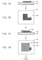
- the test vehicle was prepared in the following manner as schematically illustrated in FIG. 1A through 1G .
- electrode material EP 320 obtainable from E. I. du Pont de Nemours and Company
- electrode pattern 120 As shown in FIG. 1A , electrode material (EP 320 obtainable from E. I. du Pont de Nemours and Company) was screen-printed onto the alumina substrate to form electrode pattern 120.
- the area of the electrode was 0.3 inch by 0.3 inch (0.76 cm by 0.76 cm) and contained a protruding "finger" to allow connections to the electrode at a later stage.
- the electrode pattern was dried at 120°C for 10 minutes and fired at 930°C under copper thick-film nitrogen atmosphere firing conditions.
- dielectric material EP 310 obtainable from E.I. du Pont de Nemours and Company
- the area of the dielectric layer was approximately 0.33 Inch by 0.33 inch (0.84 cm by 0.84 cm) and covered the entirety of the electrode except for the protruding finger.
- the first dielectric layer was dried at 120°C for 10 minutes.
- a second dielectric layer was then applied, and also dried using the same conditions.
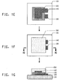
- a plan view of the dielectric pattern is shown in FIG. 1D .
- copper paste EP 320 was printed over the second dielectric layer to form electrode pattern 140.
- the electrode was 0.3 Inch by 0.3 inch (0.76 cm by 0.76 cm) but included a protruding finger that extended over the alumina substrate.
- the copper paste was dried at 120°C for 10 minutes.
- the first dielectric layer, the second dielectric layer, and the copper paste electrode were then co-fired at 930°C under copper thick-film firing conditions.
- the encapsulant composition of Example 3 was screen printed through a 180 mesh screen over the entirety of the capacitor electrode and dielectric except for the two fingers using the pattern shown in FIG. 1 F to form a 0.4 inch by 0,4 Inch (1 cm by 1 cm) encapsulant layer 150 .
- the encapsulant layer was dried for 10 minutes at 120°C.
- Another layer of encapsulant was printed with the formulation prepared In Example 4 through a 325 mesh screen over the first encapsulant layer and dried for 10 minutes at 120°C.
- a side view of the final stack is shown In FIG. 1G .
- the two layer composite encapsulant was then baked under nitrogen in a forced draft oven at 190°C for 30 minutes.
- the final cured thickness of the encapsulant was approximately 10 microns.
- the average capacitance of the capacitors was 40.4 nF
- the average loss factor was 1.5%
- the average insulation resistance was 2.4 Gohms. Coupons were then subjected to the brown oxide test described previously. The average capacitance, loss factor, and insulation resistance were 40.1 nF, 1.5%, 2.1 Gohm respectively after the treatment. Unencapsulated coupons did not survive the acid and base exposures.
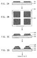
- Example 6 Preparation of Encapsulated Fired-On Foil Capacitors, Lamination with Prepreg and Core to Determine Adhesive Strength and Delamination Tendency
- Fired-on-foil capacitors were fabricated for use as a test structure using the following process.
- a 1 ounce (28 g) copper foil 210 was pretreated by applying copper paste EP 320 (obtainable from E. I. du Pont de Nemours and Company) as a preprint to the foil to form the pattern 215 and fired at 930°C under copper thick-film firing conditions.
- Each preprint pattern was approximately 1.67 cm by 1.67 cm.
- a plan view of the preprint is shown in FIG. 2B .
- dielectric material EP 310 obtainable from E.I. du Pont de Nemours and Company
- pattern 220 The area of the dielectric layer was 1.22 cm by 1.22.cm. and within the pattern of the preprint.
- the first dielectric layer was dried at 120°C for 10 minutes.
- a second dielectric layer was then applied, and also dried using the same conditions.
- copper paste EP 320 was printed over the second dielectric layer and within the area of the dielectric to form electrode pattern 230 and dried at 120°C for 10 minutes.
- the area of the electrode was 0.9 cm by 0.9 cm.
- the first dielectric layer, the second dielectric layer, and the copper paste electrode were then co-fired at 930°C under copper thick-film firing conditions.
- the encapsulant composition as described in Example 3 was printed through a 180 mesh screen over capacitors to form encapsulant layer 240 using the pattern as shown in FIG. 2E .
- the encapsulant was dried at 120°C for ten minutes.
- a second encapsulant layer was then printed directly over the first layer using the paste prepared in Example 4 with a 325 mesh screen.
- the two-layer structure was then baked for 10 min at 120°C then cured at 190°C under nitrogen for 30 minutes to yield a consolidated two-layer composite encapsulant.
- the final cured encapsulant thickness was approximately 10 microns.
- a plan view of the structure is shown in FIG. 2F .
- the component side of the foil was laminated to 1080 BT resin prepreg 250 at 375°F (191°C) at 400 psi (2.76 MPa) for 90 minutes to form the structure shown in FIG. 2G .
- the adhesion of the prepreg to the encapsulant was tested using the IPC - TM - 660 adhesion test number 2.4.9. The adhesion results are shown below.
- Some foils were also laminated with 1080 BT resin prepreg and BT core in place of copper foil, These samples were subjected to 5 successive solder floats at 260°C, each exposure lasting three minutes, to determine the tendency for the structure to delaminate during thermal cycling. Visual inspection was used to determine if delamination occurred.
Landscapes
- Engineering & Computer Science (AREA)
- Power Engineering (AREA)
- Microelectronics & Electronic Packaging (AREA)
- Chemical & Material Sciences (AREA)
- Manufacturing & Machinery (AREA)
- Inorganic Chemistry (AREA)
- Ceramic Engineering (AREA)
- Materials Engineering (AREA)
- Organic Chemistry (AREA)
- Compositions Of Macromolecular Compounds (AREA)
- Non-Metallic Protective Coatings For Printed Circuits (AREA)
- Paints Or Removers (AREA)
- Parts Printed On Printed Circuit Boards (AREA)
- Structures Or Materials For Encapsulating Or Coating Semiconductor Devices Or Solid State Devices (AREA)
- Laminated Bodies (AREA)
Claims (10)
- Composition organique d'enrobage à deux couches permettant de revêtir un ou plusieurs condensateurs en céramique formés sur feuille intégrés, ledit produit d'enrobage à deux couches comprenant une première couche d'enrobage et une deuxième couche d'enrobage dans laquelle ladite première couche d'enrobage comprend (a) un polyimide et ladite deuxième couche d'enrobage comprend (b) une résine d'oléfine cyclique contenant un époxy, (c) une résine phénolique, (d) un catalyseur époxy ; et dans laquelle ladite deuxième couche d'enrobage est en contact direct avec ladite première couche d'enrobage.
- Composition organique d'enrobage à deux couches selon la revendication 1 dans laquelle ladite première couche d'enrobage comprend un polyimide présentant une absorption d'eau de 2% ou moins et une température de transition vitreuse supérieure à 280°C.
- Composition organique d'enrobage à deux couches selon la revendication 1 dans laquelle ladite deuxième couche d'enrobage comprend une résine d'oléfine cyclique contenant un époxy présentant une absorption d'eau de 2% ou moins.
- Composition organique d'enrobage à deux couches selon la revendication 1 dans laquelle ladite deuxième couche d'enrobage comprend une résine phénolique présentant une absorption d'eau de moins de 2% ; un catalyseur époxy ; éventuellement un ou plusieurs matériaux parmi une charge isolée électriquement, un antimousse et une matière colorante et un ou plusieurs solvants organiques.
- Composition organique d'enrobage à deux couches selon la revendication 1 dans laquelle ladite première couche d'enrobage comprend en outre un ou plusieurs composants optionnels choisis dans le groupe comprenant une charge isolée électriquement, un antimousse, une matière colorante, une résine époxy, et leurs mélanges.
- Composition d'enrobage selon l'une quelconque des revendications précédentes, dans laquelle le composant polyimide est représenté par la formule générale :

- Composition d'enrobage selon la revendication 6, dans laquelle la partie restante du composant diamine est choisie parmi les groupes 3,4'-diaminodiphényléther (3,4'-ODA), 4,4'-diamino-2,2'-bis(trifluorométhyl)biphényle (TFMB), 3,3',5,5'-tétraméthylbenzidine, 2,3,5,6-tétraméthyl-1,4-phénylènediamine, 3,3'-diamino-diphénylsulfone, 3,3'-diméthylbenzidine, 3,3'-bis(trifluorométhyl)benzidine, 2,2'-bis-(p-aminophényl)hexafluoropropane, bis(trifluorométhoxy)benzidine (TFMOB), 2,2'-bis(pentafluoroéthoxy)benzidine (TFEOB), 2,2'-trifluorométhyl-4,4'-oxydianiline (OBABTF), 2-phényl-2-trifluorométhyl-bis(p-aminophényl)méthane, 2-phényl-2-trifluorométhyl-bis(m-aminophényl)méthane, 2,2'-bis(2-heptafluoroisopropoxytétrafluoroéthoxy)benzidine (DFPOB), 2,2-bis(m-aminophényl)hexafluoropropane (6-FmDA), 2,2-bis(3-amino-4-méthylphényl)hexafluoropropane, 3,6-bis(trifluorométhyl)-1,4-diaminobenzène (2TFMPDA), 1-(3,5-diaminophényl)-2,2-bis(trifluorométhyl)-3,3,4,4,5,5,5-heptafluoropentane, 3,5-diaminobenzotrifluorure (3,5-DABTF), 3,5-diamino-5-(pentafluoroéthyl) benzène, 3,5-diamino-5-(heptafluoropropyl)-benzène, 2,2'-diméthylbenzidine (DMBZ), 2,2',6,6'-tétraméthylbenzidine (TMBZ), 3,6-diamino-9,9-bis(trifluorométhyl)xanthène (6FCDAM), 3,6-diamino-9-trifluorométhyl-9-phénylxanthène (3FCDAM), 3,6-diamino-9,9-diphénylxanthène, et leurs mélanges.
- Composition d'enrobage selon l'une quelconque des revendications 1-5 dans laquelle le composant dianhydride utilisé pour préparer le composant polyimide est choisi parmi les suivants : dianhydride 3,3',4,4'-diphénylsulfone-tétracarboxylique (DSDA), 2,2-bis(3,4-dicarboxyphényl)-1,1,1,3,3,3-hexafluoropropane-dianhydride (6-FDA), 1-phényl-1,1-bis(3,4-dicarboxyphényl)-2,2,2-trifluoroéthane-dianhydride, 1,1,1,3,3,4,4,4-octylfluoro-2,2-bis(3,4-dicarboxyphényl)butane-dianhydride, 1-phényl-2,2,3,3,3-pentafluoro-1,1-bis(3,4-dicarboxylphényl)propane-dianhydride, anhydride 4,4'-oxydiphtalique (ODPA), 2,2'-bis(3,4-dicarboxyphényl)-propane-dianhydride, 2,2'-bis(3,4-dicarboxyphényl)-2-phényléthane-dianhydride, 2,3,6,7-tétracarboxy-9-trifluorométhyl-9-phénylxanthène-dianhydride (3FCDA), 2,3,6,7-tétracarboxy-9,9-bis(trifluorométhyl)xanthène-dianhydride (6FCDA), 2,3,6,7-tétracarboxy-9-méthyl-9-trifluorométhylxanthène-dianhydride (MTXDA), 2,3,6,7-tétracarboxy-9-phényl-9-méthylxanthène-dianhydride (MPXDA), 2,3,6,7-tétracarboxy-9,9-diméthylxanthène-dianhydride (NMXDA), et des combinaisons de ceux-ci.
- Composition d'enrobage selon l'une quelconque des revendications précédentes, dans laquelle la résine d'oléfine cyclique contenant un époxy comprend un polymère époxy-PNB comprenant des motifs moléculaires de formule I :


et dans laquelle le rapport molaire entre les motifs moléculaires de formule II et les motifs moléculaires de formule I dans le polymère époxy-PNB est compris entre 0 et 0,4. - Composition d'enrobage selon l'une quelconque des revendications précédentes, dans laquelle la résine phénolique est une résine phénolique dicyclopentadiène.
Applications Claiming Priority (2)
| Application Number | Priority Date | Filing Date | Title |
|---|---|---|---|
| US87459806P | 2006-12-12 | 2006-12-12 | |
| PCT/US2007/025296 WO2008073409A2 (fr) | 2006-12-12 | 2007-12-11 | Matières d'encapsulation organiques composites |
Publications (2)
| Publication Number | Publication Date |
|---|---|
| EP2092807A2 EP2092807A2 (fr) | 2009-08-26 |
| EP2092807B1 true EP2092807B1 (fr) | 2013-04-17 |
Family
ID=39512305
Family Applications (1)
| Application Number | Title | Priority Date | Filing Date |
|---|---|---|---|
| EP07862748.6A Active EP2092807B1 (fr) | 2006-12-12 | 2007-12-11 | Matières d'encapsulation organiques composites |
Country Status (7)
| Country | Link |
|---|---|
| US (1) | US8233261B2 (fr) |
| EP (1) | EP2092807B1 (fr) |
| JP (1) | JP2010512663A (fr) |
| KR (1) | KR101321198B1 (fr) |
| CN (1) | CN101617573A (fr) |
| TW (1) | TWI418266B (fr) |
| WO (1) | WO2008073409A2 (fr) |
Families Citing this family (7)
| Publication number | Priority date | Publication date | Assignee | Title |
|---|---|---|---|---|
| TW200839811A (en) * | 2006-12-12 | 2008-10-01 | Du Pont | Crystalline encapsulants |
| DE102007028238A1 (de) | 2007-06-20 | 2008-12-24 | Osram Opto Semiconductors Gmbh | Verwendung eines Metallkomplexes als p-Dotand für ein organisches halbleitendes Matrixmaterial, organisches Halbleitermaterial und organische Leuchtdiode |
| US8481626B1 (en) | 2012-01-16 | 2013-07-09 | Itron, Inc. | Wax-based encapsulant/moisture barrier for use with electronics received in water meter pits |
| US8728568B2 (en) | 2012-01-16 | 2014-05-20 | Itron, Inc. | Method for encapsulation of electronics received in water meter pits with an improved wax-based encapsulant/moisture barrier |
| US9076724B1 (en) * | 2013-09-26 | 2015-07-07 | Stats Chippac Ltd. | Integrated circuit system with debonding adhesive and method of manufacture thereof |
| JP6060945B2 (ja) | 2014-07-28 | 2017-01-18 | 株式会社村田製作所 | セラミック電子部品およびその製造方法 |
| US10446414B2 (en) | 2017-12-22 | 2019-10-15 | Texas Instruments Incorporated | Semiconductor package with filler particles in a mold compound |
Citations (1)
| Publication number | Priority date | Publication date | Assignee | Title |
|---|---|---|---|---|
| WO2007146383A1 (fr) * | 2006-06-15 | 2007-12-21 | E. I. Du Pont De Nemours And Company | Compositions encapsulantes organiques à base de polymères hétérocycliques pour la protection de composants électroniques |
Family Cites Families (8)
| Publication number | Priority date | Publication date | Assignee | Title |
|---|---|---|---|---|
| US4323948A (en) * | 1977-12-05 | 1982-04-06 | Westinghouse Electric Corp. | Capacitor structures with improved electrical stress capability |
| DE69725159T2 (de) * | 1996-10-29 | 2004-08-12 | Nippon Zeon Co., Ltd. | Modifiziertes, thermoplastisches norbornen polymer und verfahren zu seiner herstellung |
| US6317023B1 (en) | 1999-10-15 | 2001-11-13 | E. I. Du Pont De Nemours And Company | Method to embed passive components |
| US6860000B2 (en) * | 2002-02-15 | 2005-03-01 | E.I. Du Pont De Nemours And Company | Method to embed thick film components |
| US7029971B2 (en) | 2003-07-17 | 2006-04-18 | E. I. Du Pont De Nemours And Company | Thin film dielectrics for capacitors and methods of making thereof |
| US20050154105A1 (en) * | 2004-01-09 | 2005-07-14 | Summers John D. | Compositions with polymers for advanced materials |
| US7348373B2 (en) | 2004-01-09 | 2008-03-25 | E.I. Du Pont De Nemours And Company | Polyimide compositions having resistance to water sorption, and methods relating thereto |
| US7100277B2 (en) * | 2004-07-01 | 2006-09-05 | E. I. Du Pont De Nemours And Company | Methods of forming printed circuit boards having embedded thick film capacitors |
-
2007
- 2007-12-11 TW TW096147302A patent/TWI418266B/zh active
- 2007-12-11 CN CN200780043719A patent/CN101617573A/zh active Pending
- 2007-12-11 WO PCT/US2007/025296 patent/WO2008073409A2/fr active Application Filing
- 2007-12-11 EP EP07862748.6A patent/EP2092807B1/fr active Active
- 2007-12-11 KR KR1020097014419A patent/KR101321198B1/ko active IP Right Grant
- 2007-12-11 US US12/514,822 patent/US8233261B2/en active Active
- 2007-12-11 JP JP2009541342A patent/JP2010512663A/ja active Pending
Patent Citations (1)
| Publication number | Priority date | Publication date | Assignee | Title |
|---|---|---|---|---|
| WO2007146383A1 (fr) * | 2006-06-15 | 2007-12-21 | E. I. Du Pont De Nemours And Company | Compositions encapsulantes organiques à base de polymères hétérocycliques pour la protection de composants électroniques |
Also Published As
| Publication number | Publication date |
|---|---|
| EP2092807A2 (fr) | 2009-08-26 |
| WO2008073409A3 (fr) | 2008-09-12 |
| US20100067168A1 (en) | 2010-03-18 |
| JP2010512663A (ja) | 2010-04-22 |
| WO2008073409A2 (fr) | 2008-06-19 |
| KR20090087961A (ko) | 2009-08-18 |
| CN101617573A (zh) | 2009-12-30 |
| KR101321198B1 (ko) | 2013-10-23 |
| TW200850088A (en) | 2008-12-16 |
| US8233261B2 (en) | 2012-07-31 |
| TWI418266B (zh) | 2013-12-01 |
Similar Documents
| Publication | Publication Date | Title |
|---|---|---|
| US20070290379A1 (en) | Hydrophobic compositions for electronic applications | |
| EP2092807B1 (fr) | Matières d'encapsulation organiques composites | |
| US20070291440A1 (en) | Organic encapsulant compositions based on heterocyclic polymers for protection of electronic components | |
| US20070236859A1 (en) | Organic encapsulant compositions for protection of electronic components | |
| KR100874822B1 (ko) | 전자 분야용 소수성 가교성 조성물 | |
| KR101107847B1 (ko) | 결정질 봉지재 | |
| KR20090058461A (ko) | 가용성 폴리벤즈옥사졸 기재의 스크린 인쇄가능한 캡슐화제 | |
| KR101082225B1 (ko) | 폴리벤즈옥사졸로 열적으로 전환하는 폴리히드록시아미드기재 스크린 인쇄가능한 캡슐화제 | |
| EP1845130A2 (fr) | Compositions réticulables hydrophobes pour des applications électroniques |
Legal Events
| Date | Code | Title | Description |
|---|---|---|---|
| PUAI | Public reference made under article 153(3) epc to a published international application that has entered the european phase |
Free format text: ORIGINAL CODE: 0009012 |
|
| 17P | Request for examination filed |
Effective date: 20090616 |
|
| AK | Designated contracting states |
Kind code of ref document: A2 Designated state(s): AT BE BG CH CY CZ DE DK EE ES FI FR GB GR HU IE IS IT LI LT LU LV MC MT NL PL PT RO SE SI SK TR |
|
| 17Q | First examination report despatched |
Effective date: 20100128 |
|
| DAX | Request for extension of the european patent (deleted) | ||
| RAP1 | Party data changed (applicant data changed or rights of an application transferred) |
Owner name: CDA PROCESSING LIMITED LIABILITY COMPANY |
|
| GRAP | Despatch of communication of intention to grant a patent |
Free format text: ORIGINAL CODE: EPIDOSNIGR1 |
|
| GRAS | Grant fee paid |
Free format text: ORIGINAL CODE: EPIDOSNIGR3 |
|
| GRAA | (expected) grant |
Free format text: ORIGINAL CODE: 0009210 |
|
| AK | Designated contracting states |
Kind code of ref document: B1 Designated state(s): AT BE BG CH CY CZ DE DK EE ES FI FR GB GR HU IE IS IT LI LT LU LV MC MT NL PL PT RO SE SI SK TR |
|
| REG | Reference to a national code |
Ref country code: GB Ref legal event code: FG4D |
|
| REG | Reference to a national code |
Ref country code: CH Ref legal event code: EP |
|
| REG | Reference to a national code |
Ref country code: IE Ref legal event code: FG4D |
|
| REG | Reference to a national code |
Ref country code: AT Ref legal event code: REF Ref document number: 607971 Country of ref document: AT Kind code of ref document: T Effective date: 20130515 |
|
| REG | Reference to a national code |
Ref country code: DE Ref legal event code: R096 Ref document number: 602007029907 Country of ref document: DE Effective date: 20130613 |
|
| REG | Reference to a national code |
Ref country code: AT Ref legal event code: MK05 Ref document number: 607971 Country of ref document: AT Kind code of ref document: T Effective date: 20130417 |
|
| REG | Reference to a national code |
Ref country code: LT Ref legal event code: MG4D |
|
| REG | Reference to a national code |
Ref country code: NL Ref legal event code: VDEP Effective date: 20130417 |
|
| PG25 | Lapsed in a contracting state [announced via postgrant information from national office to epo] |
Ref country code: PT Free format text: LAPSE BECAUSE OF FAILURE TO SUBMIT A TRANSLATION OF THE DESCRIPTION OR TO PAY THE FEE WITHIN THE PRESCRIBED TIME-LIMIT Effective date: 20130819 Ref country code: IS Free format text: LAPSE BECAUSE OF FAILURE TO SUBMIT A TRANSLATION OF THE DESCRIPTION OR TO PAY THE FEE WITHIN THE PRESCRIBED TIME-LIMIT Effective date: 20130817 Ref country code: LT Free format text: LAPSE BECAUSE OF FAILURE TO SUBMIT A TRANSLATION OF THE DESCRIPTION OR TO PAY THE FEE WITHIN THE PRESCRIBED TIME-LIMIT Effective date: 20130417 Ref country code: SI Free format text: LAPSE BECAUSE OF FAILURE TO SUBMIT A TRANSLATION OF THE DESCRIPTION OR TO PAY THE FEE WITHIN THE PRESCRIBED TIME-LIMIT Effective date: 20130417 Ref country code: AT Free format text: LAPSE BECAUSE OF FAILURE TO SUBMIT A TRANSLATION OF THE DESCRIPTION OR TO PAY THE FEE WITHIN THE PRESCRIBED TIME-LIMIT Effective date: 20130417 Ref country code: FI Free format text: LAPSE BECAUSE OF FAILURE TO SUBMIT A TRANSLATION OF THE DESCRIPTION OR TO PAY THE FEE WITHIN THE PRESCRIBED TIME-LIMIT Effective date: 20130417 Ref country code: SE Free format text: LAPSE BECAUSE OF FAILURE TO SUBMIT A TRANSLATION OF THE DESCRIPTION OR TO PAY THE FEE WITHIN THE PRESCRIBED TIME-LIMIT Effective date: 20130417 Ref country code: ES Free format text: LAPSE BECAUSE OF FAILURE TO SUBMIT A TRANSLATION OF THE DESCRIPTION OR TO PAY THE FEE WITHIN THE PRESCRIBED TIME-LIMIT Effective date: 20130728 Ref country code: BE Free format text: LAPSE BECAUSE OF FAILURE TO SUBMIT A TRANSLATION OF THE DESCRIPTION OR TO PAY THE FEE WITHIN THE PRESCRIBED TIME-LIMIT Effective date: 20130417 Ref country code: GR Free format text: LAPSE BECAUSE OF FAILURE TO SUBMIT A TRANSLATION OF THE DESCRIPTION OR TO PAY THE FEE WITHIN THE PRESCRIBED TIME-LIMIT Effective date: 20130718 |
|
| PG25 | Lapsed in a contracting state [announced via postgrant information from national office to epo] |
Ref country code: PL Free format text: LAPSE BECAUSE OF FAILURE TO SUBMIT A TRANSLATION OF THE DESCRIPTION OR TO PAY THE FEE WITHIN THE PRESCRIBED TIME-LIMIT Effective date: 20130417 Ref country code: BG Free format text: LAPSE BECAUSE OF FAILURE TO SUBMIT A TRANSLATION OF THE DESCRIPTION OR TO PAY THE FEE WITHIN THE PRESCRIBED TIME-LIMIT Effective date: 20130717 Ref country code: LV Free format text: LAPSE BECAUSE OF FAILURE TO SUBMIT A TRANSLATION OF THE DESCRIPTION OR TO PAY THE FEE WITHIN THE PRESCRIBED TIME-LIMIT Effective date: 20130417 Ref country code: CY Free format text: LAPSE BECAUSE OF FAILURE TO SUBMIT A TRANSLATION OF THE DESCRIPTION OR TO PAY THE FEE WITHIN THE PRESCRIBED TIME-LIMIT Effective date: 20130417 |
|
| PG25 | Lapsed in a contracting state [announced via postgrant information from national office to epo] |
Ref country code: CZ Free format text: LAPSE BECAUSE OF FAILURE TO SUBMIT A TRANSLATION OF THE DESCRIPTION OR TO PAY THE FEE WITHIN THE PRESCRIBED TIME-LIMIT Effective date: 20130417 Ref country code: EE Free format text: LAPSE BECAUSE OF FAILURE TO SUBMIT A TRANSLATION OF THE DESCRIPTION OR TO PAY THE FEE WITHIN THE PRESCRIBED TIME-LIMIT Effective date: 20130417 Ref country code: DK Free format text: LAPSE BECAUSE OF FAILURE TO SUBMIT A TRANSLATION OF THE DESCRIPTION OR TO PAY THE FEE WITHIN THE PRESCRIBED TIME-LIMIT Effective date: 20130417 Ref country code: SK Free format text: LAPSE BECAUSE OF FAILURE TO SUBMIT A TRANSLATION OF THE DESCRIPTION OR TO PAY THE FEE WITHIN THE PRESCRIBED TIME-LIMIT Effective date: 20130417 |
|
| PLBE | No opposition filed within time limit |
Free format text: ORIGINAL CODE: 0009261 |
|
| STAA | Information on the status of an ep patent application or granted ep patent |
Free format text: STATUS: NO OPPOSITION FILED WITHIN TIME LIMIT |
|
| PG25 | Lapsed in a contracting state [announced via postgrant information from national office to epo] |
Ref country code: NL Free format text: LAPSE BECAUSE OF FAILURE TO SUBMIT A TRANSLATION OF THE DESCRIPTION OR TO PAY THE FEE WITHIN THE PRESCRIBED TIME-LIMIT Effective date: 20130417 Ref country code: IT Free format text: LAPSE BECAUSE OF FAILURE TO SUBMIT A TRANSLATION OF THE DESCRIPTION OR TO PAY THE FEE WITHIN THE PRESCRIBED TIME-LIMIT Effective date: 20130417 Ref country code: RO Free format text: LAPSE BECAUSE OF FAILURE TO SUBMIT A TRANSLATION OF THE DESCRIPTION OR TO PAY THE FEE WITHIN THE PRESCRIBED TIME-LIMIT Effective date: 20130417 |
|
| 26N | No opposition filed |
Effective date: 20140120 |
|
| REG | Reference to a national code |
Ref country code: DE Ref legal event code: R097 Ref document number: 602007029907 Country of ref document: DE Effective date: 20140120 |
|
| REG | Reference to a national code |
Ref country code: CH Ref legal event code: PL |
|
| PG25 | Lapsed in a contracting state [announced via postgrant information from national office to epo] |
Ref country code: LU Free format text: LAPSE BECAUSE OF FAILURE TO SUBMIT A TRANSLATION OF THE DESCRIPTION OR TO PAY THE FEE WITHIN THE PRESCRIBED TIME-LIMIT Effective date: 20131211 Ref country code: MC Free format text: LAPSE BECAUSE OF FAILURE TO SUBMIT A TRANSLATION OF THE DESCRIPTION OR TO PAY THE FEE WITHIN THE PRESCRIBED TIME-LIMIT Effective date: 20130417 |
|
| REG | Reference to a national code |
Ref country code: IE Ref legal event code: MM4A |
|
| PG25 | Lapsed in a contracting state [announced via postgrant information from national office to epo] |
Ref country code: CH Free format text: LAPSE BECAUSE OF NON-PAYMENT OF DUE FEES Effective date: 20131231 Ref country code: IE Free format text: LAPSE BECAUSE OF NON-PAYMENT OF DUE FEES Effective date: 20131211 Ref country code: LI Free format text: LAPSE BECAUSE OF NON-PAYMENT OF DUE FEES Effective date: 20131231 |
|
| PG25 | Lapsed in a contracting state [announced via postgrant information from national office to epo] |
Ref country code: TR Free format text: LAPSE BECAUSE OF FAILURE TO SUBMIT A TRANSLATION OF THE DESCRIPTION OR TO PAY THE FEE WITHIN THE PRESCRIBED TIME-LIMIT Effective date: 20130417 |
|
| PG25 | Lapsed in a contracting state [announced via postgrant information from national office to epo] |
Ref country code: HU Free format text: LAPSE BECAUSE OF FAILURE TO SUBMIT A TRANSLATION OF THE DESCRIPTION OR TO PAY THE FEE WITHIN THE PRESCRIBED TIME-LIMIT; INVALID AB INITIO Effective date: 20071211 |
|
| PG25 | Lapsed in a contracting state [announced via postgrant information from national office to epo] |
Ref country code: MT Free format text: LAPSE BECAUSE OF FAILURE TO SUBMIT A TRANSLATION OF THE DESCRIPTION OR TO PAY THE FEE WITHIN THE PRESCRIBED TIME-LIMIT Effective date: 20130417 |
|
| REG | Reference to a national code |
Ref country code: FR Ref legal event code: PLFP Year of fee payment: 9 |
|
| REG | Reference to a national code |
Ref country code: FR Ref legal event code: PLFP Year of fee payment: 10 |
|
| REG | Reference to a national code |
Ref country code: FR Ref legal event code: PLFP Year of fee payment: 11 |
|
| P01 | Opt-out of the competence of the unified patent court (upc) registered |
Effective date: 20230527 |
|
| PGFP | Annual fee paid to national office [announced via postgrant information from national office to epo] |
Ref country code: GB Payment date: 20231108 Year of fee payment: 17 |
|
| PGFP | Annual fee paid to national office [announced via postgrant information from national office to epo] |
Ref country code: FR Payment date: 20231108 Year of fee payment: 17 Ref country code: DE Payment date: 20231108 Year of fee payment: 17 |