EP2091084A1 - A dye sensitized solar battery and a working electrode thereof - Google Patents
A dye sensitized solar battery and a working electrode thereof Download PDFInfo
- Publication number
- EP2091084A1 EP2091084A1 EP07816412A EP07816412A EP2091084A1 EP 2091084 A1 EP2091084 A1 EP 2091084A1 EP 07816412 A EP07816412 A EP 07816412A EP 07816412 A EP07816412 A EP 07816412A EP 2091084 A1 EP2091084 A1 EP 2091084A1
- Authority
- EP
- European Patent Office
- Prior art keywords
- working electrode
- semi
- conductive material
- filamentous
- conductive substrate
- Prior art date
- Legal status (The legal status is an assumption and is not a legal conclusion. Google has not performed a legal analysis and makes no representation as to the accuracy of the status listed.)
- Ceased
Links
Images


Classifications
-
- H—ELECTRICITY
- H01—ELECTRIC ELEMENTS
- H01G—CAPACITORS; CAPACITORS, RECTIFIERS, DETECTORS, SWITCHING DEVICES, LIGHT-SENSITIVE OR TEMPERATURE-SENSITIVE DEVICES OF THE ELECTROLYTIC TYPE
- H01G9/00—Electrolytic capacitors, rectifiers, detectors, switching devices, light-sensitive or temperature-sensitive devices; Processes of their manufacture
- H01G9/20—Light-sensitive devices
- H01G9/2068—Panels or arrays of photoelectrochemical cells, e.g. photovoltaic modules based on photoelectrochemical cells
- H01G9/2086—Photoelectrochemical cells in the form of a fiber
-
- H—ELECTRICITY
- H01—ELECTRIC ELEMENTS
- H01G—CAPACITORS; CAPACITORS, RECTIFIERS, DETECTORS, SWITCHING DEVICES, LIGHT-SENSITIVE OR TEMPERATURE-SENSITIVE DEVICES OF THE ELECTROLYTIC TYPE
- H01G9/00—Electrolytic capacitors, rectifiers, detectors, switching devices, light-sensitive or temperature-sensitive devices; Processes of their manufacture
- H01G9/20—Light-sensitive devices
- H01G9/2027—Light-sensitive devices comprising an oxide semiconductor electrode
- H01G9/2031—Light-sensitive devices comprising an oxide semiconductor electrode comprising titanium oxide, e.g. TiO2
-
- H—ELECTRICITY
- H10—SEMICONDUCTOR DEVICES; ELECTRIC SOLID-STATE DEVICES NOT OTHERWISE PROVIDED FOR
- H10K—ORGANIC ELECTRIC SOLID-STATE DEVICES
- H10K30/00—Organic devices sensitive to infrared radiation, light, electromagnetic radiation of shorter wavelength or corpuscular radiation
- H10K30/50—Photovoltaic [PV] devices
- H10K30/53—Photovoltaic [PV] devices in the form of fibres or tubes, e.g. photovoltaic fibres
-
- Y—GENERAL TAGGING OF NEW TECHNOLOGICAL DEVELOPMENTS; GENERAL TAGGING OF CROSS-SECTIONAL TECHNOLOGIES SPANNING OVER SEVERAL SECTIONS OF THE IPC; TECHNICAL SUBJECTS COVERED BY FORMER USPC CROSS-REFERENCE ART COLLECTIONS [XRACs] AND DIGESTS
- Y02—TECHNOLOGIES OR APPLICATIONS FOR MITIGATION OR ADAPTATION AGAINST CLIMATE CHANGE
- Y02E—REDUCTION OF GREENHOUSE GAS [GHG] EMISSIONS, RELATED TO ENERGY GENERATION, TRANSMISSION OR DISTRIBUTION
- Y02E10/00—Energy generation through renewable energy sources
- Y02E10/50—Photovoltaic [PV] energy
- Y02E10/542—Dye sensitized solar cells
Definitions
- the present invention relates to the field of solar cell technology, and particularly, to a dye sensitized solar cell's construction and a working electrode thereof.
- a dye sensitized solar cell comprises mainly of a working electrode, an electrolyte layer and a counter electrode, in which the electrolyte layer can be solid or liquid as well.
- the working electrode comprises a conductive substrate, a porous film of semi-conductor material and dye molecules for sensitizing.
- the conductive substrate of the working electrode is planar structured.
- planar structure of conventional solar cells confines their own applicable range enormously, and constrains the ideation of designers.
- higher driving voltage > 3V
- a solar module formed by a plurality of cells in a manner of series connection and the like is required for supplying power.
- the conventional connection approach with additional wires makes the already narrow space inside a microelectronic element even more deficient.
- an object of the present invention is to provide a solar cell which is freely deformable, accessible for series-parallel connection, low in cost, and is specifically suitable for narrow and irregular-shaped space requiring specific driving power supply.
- a working electrode of a dye sensitized solar cell comprising a filamentous conductive substrate and a sensitized semi-conductor film, wherein the sensitized semi-conductor film is a porous film structure composed of semi-conductor particles of different sizes absorbed with sensitizing dye molecules, and the sensitized semi-conductor film is coated on the outer surface of the filamentous conductive substrate.
- the filamentous conductive substrate can be a solid or hollow structure made of a conductive material, and can also comprise a core and several layers of sheath.
- the core is of a conductive or nonconductive material.
- the sheaths surround outside the core layer by layer, and the outermost layer of sheath is of a conductive material.
- the conductive material is an organic conductive material or an inorganic conductive material or an organic/inorganic composite conductive material.
- the filamentous conductive substrate can be formed not only by one filament, but also by two or more filaments collectively in a manner of intimately arranging, wrapping around each other, twisting with each other and the like.
- the surface of the filamentous conductive substrate can be further coated by a layer of compact semi-conductor or insulator material.
- the sensitized semi-conductor film coated on the filamentous conductive substrate may be 1 micron to 100 microns in thickness.
- a dye sensitized solar cell comprises a working electrode, an electrolyte layer and a counter electrode.
- the working electrode is made up of a filamentous conductive substrate and a sensitized semi-conductor film, wherein the sensitized semi-conductor film is a porous film structure composed of semi-conductor particles of different sizes absorbed with sensitizing dye molecules, and the sensitized semi-conductor film is coated on the outer surface of the filamentous conductive substrate.
- the electrolyte fills in the interspace between the working electrode and the counter electrode.
- the electrolyte layer can be a liquid electrolyte, a solid inorganic or organic semi-conductor, an ionic liquid, an inorganic or organic gel electrolyte or a solid inorganic conductor based on fast-transfer ions.
- the counter electrode can be a conductor of any shape, such as filamentous, planar or blocky, or it can also consist of conductors with one or more of the three shapes mentioned above collectively in a way of intimately arranging, entwisting with each other and the like.
- the counter electrode can be a solid or hollow structure made of a conductive material, and it can also include a core and several layers of sheath, where the core is a conductive or nonconductive material with the sheaths covering outside layer by layer, and the outermost layer is of a conductive material.
- the conductive material is an organic conductive material or inorganic conductive material or organic/inorganic composite conductive material.
- the external surface of the counter electrode can be a continuous or noncontinuous, compact or porous surface having flexure or bending of any curvature.
- the surface of the counter electrode may be further coated with a layer of catalyst which can be 1 nm to 1000 nm in thickness.
- the working electrode is joined with the counter electrode in a manner of entwisting, intimately juxtaposition or attachment and the like.
- the interstice between the working electrode and the counter electrode is in a range of 0.001 mm to 1 cm.
- the present invention is a dye sensitized solar cell in which its working electrode utilizes filamentous conductive substrate structure. Its advantages include source abundance, small volume, easiness of deformation, processing convenience and accessibility for series-parallel connection.
- the present invention provides a cheap and highly efficient solution for solar energy power supply in a narrow and irregular-shaped space.
- the working electrode of the dye sensitized solar cell comprises a filamentous conductive substrate 1 and a sensitized semi-conductor film 2, wherein the sensitized semi-conductor film 2 is a porous film structure composed of semi-conductor particles of different sizes absorbed with sensitizing dye molecules, and the sensitized semi-conductor film 2 is coated on the outer surface of the filamentous conductive substrate 1.
- the sensitized semi-conductor film of the working electrode in the dye sensitized solar cell is prepared according to the following procedure: a semi-conductor material is spray coated and sintered several times on the filamentous conductive substrate, and the filamentous conductive substrate with the sintered semi-conductor material is placed in a dye for sensitization.
- the semi-conductor material is any semi-conductor material suitable for the working electrode of the dye sensitized solar cell, most typically nanoscale TiO 2 , ZnO and the like.
- the size and distribution of the nano particles are the same as those of the nano particles used for general dye sensitized solar cells.
- the application process thereof can follow conventional methods, such as spray coating, print coating, immersion coating, dip coating, doctor blade coating and the like.
- All of the dyes suitable for conventional dye sensitized solar cells are also suitable for sensitizing the semi-conductor material of the present working electrode, and completely identical sensitizing methods can be applied.
- the sensitized semi-conductor film 2 coated on the filamentous conductive substrate 1 can be 1 micron to 100 microns in thickness.
- the diameter of the filamentous conductive substrate 1 does not exceed 1 mm in general, and its apparent resistivity is ⁇ 100 ohm cm -1 .
- the filamentous conductive substrate 1 may have a filamentous structure made of metal filaments such as stainless steel filaments, alloy filaments and the like, or nonmetal conductive filaments such as carbon fibers, conductive polymers, inorganic conductive compound fibers and organic/inorganic composite conductive fibers or the like.
- a conductive material sheath can also be applied on the outer surface of the filamentous core made from conductive or nonconductive materials, or the filamentous conductive substrate 1 can also be made by coating a conductive material outside a gas medium or a vacuum medium.
- the filamentous conductive substrate can be formed not only by one filament, but also by two or more filaments collectively in a way of intimately arranging, wrapping around each other, twisting with each other, and the like.
- a stainless steel filament approximately 100 microns in diameter is used as the filamentous conductive substrate 1 of the working electrode; and a Pt filament approximately 100 microns in diameter is used as the counter electrode 4.
- the effective length of the cell prepared is 5 cm 2 .
- the detailed preparation procedure for the working electrode is as follows:
- the prepared stainless steel filament is washed with an organic solvent, such as acetone etc., and then washed with a substrate cleanser. Thereafter, the stainless steel filament is incandesced at 400°C-500°C for 15 minutes, and naturally cooled at room temperature. Under the roast of an infrared lamp, the incandesced stainless steel filament is spray coated with a solution of tetraethyl titanate/acetylacetone in ethanol, and then sintered again at 500°C for 30 minutes, and naturally cooled, thus a compact layer of semi-conductor material TiO 2 about 0.9 micron in thickness on the stainless steel filament is obtained.
- an organic solvent such as acetone etc.
- the semi-conductor material TiO 2 emulsion normally used in dye sensitized solar cells is spray coated on the compact layer, and then sintered at 500 °C for 30 minutes. After the above spray coating and sintering processes are repeated twice, the overall thickness of the semi-conductor material TiO 2 layer on the stainless steel filament reaches 4-9 microns.
- the sintered working electrode 6 comprising semi-conductor material TiO 2 is appropriately wrapped with the Pt filament counter electrode 5, it is placed in N3 dye/ethanol solution at a concentration of 3 ⁇ 10 -4 mole/L for 12 hours or more, and then removed from the solution and air dried.
- the sensitized semi-conductor film 2 is coated on the surface of the filamentous conductive substrate 1.
- the interfacial adhesion characteristic and the like it may be considered to physically or chemically modify the surface of the filament-structured filamentous conductive substrate 1, such as surface treatment, surface coating, etc.; for example, in order to improve the cell property, a compact layer 3 made of a semi-conductor or insulating material can further be coated on the surface of the filamentous conductive substrate 1 to prevent the electrolyte 5 from directly contacting with the filamentous conductive substrate 1.
- the method for preparing the compact layer are sputtering, vacuum thermal evaporation plating, spray coating, and electrochemistry method.
- the electrolyte 5 After soaked in a standard electrolyte of normal liquid dye sensitized solar cells for 5 seconds, the electrolyte 5 is filled in the interspace between the filamentous working electrode 6 and the counter electrode 4, thus the dye sensitized solar cell of the present invention is produced.
- the cell property is measured under the condition of AM 1.5 (ASTM E892) and one time sun light intensity. The results obtained are: cell open circuit voltage is 580 mV, the short circuit current per centimeter length is 0.025 mA, and the overall photoelectric conversion efficiency is 0.91%.
- the counter electrode can be a solid or hollow structure made of conductive materials, or it can consist of a core and several layers of sheath.
- the core and the sheath can be made from conductive or nonconductive materials, while the outermost layer of sheath coated is made of conductive materials.
- the conductive material used in the counter electrode 4 can be organic conductive material, inorganic conductive material (including metallic material) or organic/inorganic composite conductive material.
- a highly efficient catalyst layer can be added on the surface of the counter electrode 4, such as plating Pt on the stainless steel filament surface.
- the external surface of the counter electrode 4 can be a continuous or noncontinuous, compact or porous surface having a flexure or bending of any curvature.
- the filamentous working electrode 6 can be arranged with the outer surface of the counter electrode 4 by wrapping, intimately juxtaposition or attaching. The distance between the filamentous working electrode 6 and the outer surface of the counter electrode 4 is in a range of 0.001 mm to 1 cm.
- the preparation method for the filamentous working electrode 7 of the dye sensitized solar cell is the same as that for the filamentous working electrode 6 described in embodiment I of the present invention.
- the filamentous conductive substrate of the filamentous working electrode 7 utilizes carbon fibers with a diameter of 5 microns.
- the counter electrode 8 is a flexible planar conductor.
- the filamentous working electrode 7 can be arranged with the outer surface of the counter electrode 8 by intimately juxtaposition or attaching, and the interstice there between is filled with electrolyte 9.
- the electrolyte 9 can be any standard electrolyte system normally used in the preparation of dye sensitized solar cells. In the present embodiment, solid CuI electrolyte is used.
- the cell property is measured under the condition of AM 1.5 (ASTM E892) and one time sun light intensity. The results obtained are: cell open circuit voltage is 500 mV, the short circuit current per centimeter length reaches 0.030 mA, and the overall photoelectric conversion efficiency is 3%.
- the present invention discloses a working electrode of a dye sensitized solar cell and a dye sensitized solar cell structure based on it.
- the application conditions and examples described above are not for the purpose of limiting the present invention. Any skilled in the art can make various change and modification without departing from the spirit and scope of the present invention, therefore the range of protection of the present invention is defined by the scope of the claims.
Landscapes
- Chemical & Material Sciences (AREA)
- Chemical Kinetics & Catalysis (AREA)
- Electrochemistry (AREA)
- Engineering & Computer Science (AREA)
- Power Engineering (AREA)
- Microelectronics & Electronic Packaging (AREA)
- Hybrid Cells (AREA)
- Photovoltaic Devices (AREA)
Abstract
Description
- The present invention relates to the field of solar cell technology, and particularly, to a dye sensitized solar cell's construction and a working electrode thereof.
- A dye sensitized solar cell comprises mainly of a working electrode, an electrolyte layer and a counter electrode, in which the electrolyte layer can be solid or liquid as well. The working electrode comprises a conductive substrate, a porous film of semi-conductor material and dye molecules for sensitizing. Limited by the material and processing technology of conventional solar cells, normally the conductive substrate of the working electrode is planar structured. When assembling a solar module, it is only possible to connect from single cells by additional wires. In many circumstances, especially the portable electronic devices that are developing fast nowadays, the available space is very limited and of irregular shape, and even varies as the application situation changes (such as highly integrated intelligent garments, outer decorations, etc.). The planar structure of conventional solar cells confines their own applicable range enormously, and constrains the ideation of designers. In addition, in the power supply of a real electronic circuit, higher driving voltage (> 3V) is often required, but it is not necessary for the current to be high, therefore a solar module formed by a plurality of cells in a manner of series connection and the like is required for supplying power. The conventional connection approach with additional wires makes the already narrow space inside a microelectronic element even more deficient.
- In addition, the main bottleneck that limits a large scale application of dye sensitized solar cells lies in the cost. Due to the limitation by process, usually the high manufacturing cost of conventional planar photovoltaic cells with special shapes can hardly be accepted in the civil grade commercialized application.
- Aiming at the problems and disadvantages of the existing solar cells, an object of the present invention is to provide a solar cell which is freely deformable, accessible for series-parallel connection, low in cost, and is specifically suitable for narrow and irregular-shaped space requiring specific driving power supply.
- The above object of the present invention is achieved by the following technical solutions: a working electrode of a dye sensitized solar cell, comprising a filamentous conductive substrate and a sensitized semi-conductor film, wherein the sensitized semi-conductor film is a porous film structure composed of semi-conductor particles of different sizes absorbed with sensitizing dye molecules, and the sensitized semi-conductor film is coated on the outer surface of the filamentous conductive substrate.
- The filamentous conductive substrate can be a solid or hollow structure made of a conductive material, and can also comprise a core and several layers of sheath. The core is of a conductive or nonconductive material. The sheaths surround outside the core layer by layer, and the outermost layer of sheath is of a conductive material. The conductive material is an organic conductive material or an inorganic conductive material or an organic/inorganic composite conductive material.
- The filamentous conductive substrate can be formed not only by one filament, but also by two or more filaments collectively in a manner of intimately arranging, wrapping around each other, twisting with each other and the like.
- The surface of the filamentous conductive substrate can be further coated by a layer of compact semi-conductor or insulator material.
- The sensitized semi-conductor film coated on the filamentous conductive substrate may be 1 micron to 100 microns in thickness.
- A dye sensitized solar cell comprises a working electrode, an electrolyte layer and a counter electrode. The working electrode is made up of a filamentous conductive substrate and a sensitized semi-conductor film, wherein the sensitized semi-conductor film is a porous film structure composed of semi-conductor particles of different sizes absorbed with sensitizing dye molecules, and the sensitized semi-conductor film is coated on the outer surface of the filamentous conductive substrate. The electrolyte fills in the interspace between the working electrode and the counter electrode.
- The electrolyte layer can be a liquid electrolyte, a solid inorganic or organic semi-conductor, an ionic liquid, an inorganic or organic gel electrolyte or a solid inorganic conductor based on fast-transfer ions.
- The counter electrode can be a conductor of any shape, such as filamentous, planar or blocky, or it can also consist of conductors with one or more of the three shapes mentioned above collectively in a way of intimately arranging, entwisting with each other and the like. The counter electrode can be a solid or hollow structure made of a conductive material, and it can also include a core and several layers of sheath, where the core is a conductive or nonconductive material with the sheaths covering outside layer by layer, and the outermost layer is of a conductive material. The conductive material is an organic conductive material or inorganic conductive material or organic/inorganic composite conductive material. The external surface of the counter electrode can be a continuous or noncontinuous, compact or porous surface having flexure or bending of any curvature.
- The surface of the counter electrode may be further coated with a layer of catalyst which can be 1 nm to 1000 nm in thickness.
- The working electrode is joined with the counter electrode in a manner of entwisting, intimately juxtaposition or attachment and the like. The interstice between the working electrode and the counter electrode is in a range of 0.001 mm to 1 cm.
- The present invention is a dye sensitized solar cell in which its working electrode utilizes filamentous conductive substrate structure. Its advantages include source abundance, small volume, easiness of deformation, processing convenience and accessibility for series-parallel connection. The present invention provides a cheap and highly efficient solution for solar energy power supply in a narrow and irregular-shaped space.
- The present invention will be described in details below with reference to the drawings.
-
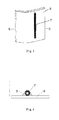
Figure 1 is an axial sectional structural schematic diagram of a filamentous working electrode of a dye sensitized solar cell in embodiment 1 of the present invention; -
Figure 2 is a radial sectional structural schematic diagram of a filamentous working electrode of a dye sensitized solar cell in embodiment 1 of the present invention; -
Figure 3 is a side structural schematic diagram of a dye sensitized solar cell used in embodiment 1 of the present invention; -
Figure 4 is a sectional structural schematic diagram taken along A-A inFigure 3 ; - In
Figures 1-4 : 1-filamentous conductive substrate, 2-sensitized semi-conductor film, 3-compact layer, 4-counter electrode, 5-electrolyte, 6-filamentous working electrode. -
Figure 5 is a top view structural schematic diagram of the dye sensitized solar cell used inembodiment 2 of the present invention; -
Figure 6 is a structural schematic diagram of the surface section taken along B-B inFigure 5 ; - In
Figure 5 and Figure 6 : 7-filamentous working electrode, 8-counter electrode, 9-electrolyte. - As shown in
Figure 1 and Figure 2 , the working electrode of the dye sensitized solar cell comprises a filamentous conductive substrate 1 and a sensitizedsemi-conductor film 2, wherein the sensitizedsemi-conductor film 2 is a porous film structure composed of semi-conductor particles of different sizes absorbed with sensitizing dye molecules, and the sensitizedsemi-conductor film 2 is coated on the outer surface of the filamentous conductive substrate 1. - The sensitized semi-conductor film of the working electrode in the dye sensitized solar cell is prepared according to the following procedure: a semi-conductor material is spray coated and sintered several times on the filamentous conductive substrate, and the filamentous conductive substrate with the sintered semi-conductor material is placed in a dye for sensitization.
- The semi-conductor material is any semi-conductor material suitable for the working electrode of the dye sensitized solar cell, most typically nanoscale TiO2, ZnO and the like. The size and distribution of the nano particles are the same as those of the nano particles used for general dye sensitized solar cells. The application process thereof can follow conventional methods, such as spray coating, print coating, immersion coating, dip coating, doctor blade coating and the like.
- All of the dyes suitable for conventional dye sensitized solar cells are also suitable for sensitizing the semi-conductor material of the present working electrode, and completely identical sensitizing methods can be applied.
- The sensitized
semi-conductor film 2 coated on the filamentous conductive substrate 1 can be 1 micron to 100 microns in thickness. - In order to ensure good flexibility while ensuring enough mechanical strength and conductivity, the diameter of the filamentous conductive substrate 1 does not exceed 1 mm in general, and its apparent resistivity is < 100 ohm cm-1.
- The filamentous conductive substrate 1 may have a filamentous structure made of metal filaments such as stainless steel filaments, alloy filaments and the like, or nonmetal conductive filaments such as carbon fibers, conductive polymers, inorganic conductive compound fibers and organic/inorganic composite conductive fibers or the like. A conductive material sheath can also be applied on the outer surface of the filamentous core made from conductive or nonconductive materials, or the filamentous conductive substrate 1 can also be made by coating a conductive material outside a gas medium or a vacuum medium.
- The filamentous conductive substrate can be formed not only by one filament, but also by two or more filaments collectively in a way of intimately arranging, wrapping around each other, twisting with each other, and the like.
- With reference to
Figure 3 and Figure 4 , a stainless steel filament approximately 100 microns in diameter is used as the filamentous conductive substrate 1 of the working electrode; and a Pt filament approximately 100 microns in diameter is used as thecounter electrode 4. The effective length of the cell prepared is 5 cm2. The detailed preparation procedure for the working electrode is as follows: - First, the prepared stainless steel filament is washed with an organic solvent, such as acetone etc., and then washed with a substrate cleanser. Thereafter, the stainless steel filament is incandesced at 400°C-500°C for 15 minutes, and naturally cooled at room temperature. Under the roast of an infrared lamp, the incandesced stainless steel filament is spray coated with a solution of tetraethyl titanate/acetylacetone in ethanol, and then sintered again at 500°C for 30 minutes, and naturally cooled, thus a compact layer of semi-conductor material TiO2 about 0.9 micron in thickness on the stainless steel filament is obtained. The semi-conductor material TiO2 emulsion normally used in dye sensitized solar cells is spray coated on the compact layer, and then sintered at 500 °C for 30 minutes. After the above spray coating and sintering processes are repeated twice, the overall thickness of the semi-conductor material TiO2 layer on the stainless steel filament reaches 4-9 microns. After the sintered working electrode 6 comprising semi-conductor material TiO2 is appropriately wrapped with the Pt filament counter electrode 5, it is placed in N3 dye/ethanol solution at a concentration of 3×10⁻⁴ mole/L for 12 hours or more, and then removed from the solution and air dried. The sensitized
semi-conductor film 2 is coated on the surface of the filamentous conductive substrate 1. - In order to improve the conductivity, activity and stability of the working electrode, as well as the charge transfer from the semi-conductor to the filamentous conductive substrate, the interfacial adhesion characteristic and the like, it may be considered to physically or chemically modify the surface of the filament-structured filamentous conductive substrate 1, such as surface treatment, surface coating, etc.; for example, in order to improve the cell property, a
compact layer 3 made of a semi-conductor or insulating material can further be coated on the surface of the filamentous conductive substrate 1 to prevent the electrolyte 5 from directly contacting with the filamentous conductive substrate 1. - The method for preparing the compact layer are sputtering, vacuum thermal evaporation plating, spray coating, and electrochemistry method.
- After soaked in a standard electrolyte of normal liquid dye sensitized solar cells for 5 seconds, the electrolyte 5 is filled in the interspace between the filamentous working electrode 6 and the
counter electrode 4, thus the dye sensitized solar cell of the present invention is produced. - The cell property is measured under the condition of AM 1.5 (ASTM E892) and one time sun light intensity. The results obtained are: cell open circuit voltage is 580 mV, the short circuit current per centimeter length is 0.025 mA, and the overall photoelectric conversion efficiency is 0.91%.
- The counter electrode can be a solid or hollow structure made of conductive materials, or it can consist of a core and several layers of sheath. The core and the sheath can be made from conductive or nonconductive materials, while the outermost layer of sheath coated is made of conductive materials. The conductive material used in the
counter electrode 4 can be organic conductive material, inorganic conductive material (including metallic material) or organic/inorganic composite conductive material. - In order to improve the electrochemical activity of the
counter electrode 4 while decreasing its cost, a highly efficient catalyst layer can be added on the surface of thecounter electrode 4, such as plating Pt on the stainless steel filament surface. - The external surface of the
counter electrode 4 can be a continuous or noncontinuous, compact or porous surface having a flexure or bending of any curvature. The filamentous working electrode 6 can be arranged with the outer surface of thecounter electrode 4 by wrapping, intimately juxtaposition or attaching. The distance between the filamentous working electrode 6 and the outer surface of thecounter electrode 4 is in a range of 0.001 mm to 1 cm. - As shown in
Figure 5 and Figure 6 , the preparation method for thefilamentous working electrode 7 of the dye sensitized solar cell is the same as that for the filamentous working electrode 6 described in embodiment I of the present invention. Here, the filamentous conductive substrate of thefilamentous working electrode 7 utilizes carbon fibers with a diameter of 5 microns. - The
counter electrode 8 is a flexible planar conductor. Thefilamentous working electrode 7 can be arranged with the outer surface of thecounter electrode 8 by intimately juxtaposition or attaching, and the interstice there between is filled withelectrolyte 9. Theelectrolyte 9 can be any standard electrolyte system normally used in the preparation of dye sensitized solar cells. In the present embodiment, solid CuI electrolyte is used. - The cell property is measured under the condition of AM 1.5 (ASTM E892) and one time sun light intensity. The results obtained are: cell open circuit voltage is 500 mV, the short circuit current per centimeter length reaches 0.030 mA, and the overall photoelectric conversion efficiency is 3%.
- To sum up, the present invention discloses a working electrode of a dye sensitized solar cell and a dye sensitized solar cell structure based on it. The application conditions and examples described above are not for the purpose of limiting the present invention. Any skilled in the art can make various change and modification without departing from the spirit and scope of the present invention, therefore the range of protection of the present invention is defined by the scope of the claims.
Claims (12)
- A working electrode of a dye sensitized solar cell, characterized in that the working electrode comprises a filamentous conductive substrate and a sensitized semi-conductor film, wherein the sensitized semi-conductor film is a porous film structure composed of semi-conductor particles of different sizes absorbed with sensitizing dye molecules, and the sensitized semi-conductor film is coated on the outer surface of the filamentous conductive substrate.
- The working electrode according to claim 1, characterized in that the filamentous conductive substrate is made of a conductive material, and it has a solid or hollow structure.
- The working electrode according to claim 1, characterized in that the filamentous conductive substrate comprises a core and several layers of sheath, and the core and the sheaths are made of conductive material or nonconductive material, and the sheaths surround outside the core layer by layer, and the outermost layer uses a conductive material.
- The working electrode according to claim 1, 2 or 3, characterized in that the outer surface of the filamentous conductive substrate is coated with a layer of compact semi-conductor or insulator material.
- The working electrode according to claim 1, characterized in that the thickness of the sensitized semi-conductor film is in a range of 1 micron to 100 microns.
- The working electrode according to claim 1, 2 or 3, characterized in that the conductive material is an organic conductive material or inorganic conductive material or organic/inorganic composite conductive material.
- A dye sensitized solar cell comprising a working electrode, an electrolyte layer and a counter electrode, characterized in that the working electrode is composed of a filamentous conductive substrate and a sensitized semi-conductor film, wherein the sensitized semi-conductor film is a porous film structure composed of semi-conductor particles of different sizes absorbed with sensitizing dye molecules, and the sensitized semi-conductor film is coated on the outer surface of the filamentous conductive substrate, and the electrolyte fills in the interspace between the working electrode and the counter electrode.
- The cell according to claim 7, characterized in that the counter electrode is made of a conductive material, and it is a solid structure or hollow structure.
- The cell according to claim 7, characterized in that the counter electrode comprises a core and several layers of sheaths, wherein the core is a conductive material or nonconductive material, and the sheaths surround outside the core layer by layer, and the outermost layer of sheath is a conductive material.
- The cell according to claim 8 or 9, characterized in that the conductive material is an organic conductive material or inorganic conductive material or organic/inorganic composite conductive material.
- The cell according to claim 7, 8 or 9, characterized in that the surface of the counter electrode is coated with a catalyst layer, and the thickness of the catalyst layer is in a range of 1 nm to 1000 nm.
- The cell according to claim 7, 8 or 9, characterized in that the working electrode is joined with the counter electrode by wrapping, intimately juxtaposition or attaching, and the interstice between the working electrode and the counter electrode is in a range of 0.001 mm to 1 cm.
Priority Applications (1)
| Application Number | Priority Date | Filing Date | Title |
|---|---|---|---|
| EP12181001A EP2528101A3 (en) | 2006-11-10 | 2007-09-21 | Dye sensitized solar cell |
Applications Claiming Priority (2)
| Application Number | Priority Date | Filing Date | Title |
|---|---|---|---|
| CNB2006101144547A CN100505325C (en) | 2006-11-10 | 2006-11-10 | Dye sensitization solar cell and working electrode thereof |
| PCT/CN2007/002796 WO2008055404A1 (en) | 2006-11-10 | 2007-09-21 | A dye sensitized solar battery and a working electrode thereof |
Publications (2)
| Publication Number | Publication Date |
|---|---|
| EP2091084A1 true EP2091084A1 (en) | 2009-08-19 |
| EP2091084A4 EP2091084A4 (en) | 2010-01-20 |
Family
ID=39364172
Family Applications (2)
| Application Number | Title | Priority Date | Filing Date |
|---|---|---|---|
| EP12181001A Withdrawn EP2528101A3 (en) | 2006-11-10 | 2007-09-21 | Dye sensitized solar cell |
| EP07816412A Ceased EP2091084A4 (en) | 2006-11-10 | 2007-09-21 | SOLAR BATTERY SENSITIZED BY A DYE AND ITS WORKING ELECTRODE |
Family Applications Before (1)
| Application Number | Title | Priority Date | Filing Date |
|---|---|---|---|
| EP12181001A Withdrawn EP2528101A3 (en) | 2006-11-10 | 2007-09-21 | Dye sensitized solar cell |
Country Status (5)
| Country | Link |
|---|---|
| US (1) | US20100037949A1 (en) |
| EP (2) | EP2528101A3 (en) |
| JP (1) | JP2010509715A (en) |
| CN (1) | CN100505325C (en) |
| WO (1) | WO2008055404A1 (en) |
Families Citing this family (9)
| Publication number | Priority date | Publication date | Assignee | Title |
|---|---|---|---|---|
| KR101027493B1 (en) | 2009-12-28 | 2011-04-06 | 재단법인대구경북과학기술원 | Solar cell using wire array and manufacturing method thereof |
| KR100994902B1 (en) * | 2010-04-06 | 2010-11-16 | 서울대학교산학협력단 | Flexible dye-sensitized solar cell and preparation method thereof |
| CN102568845B (en) * | 2010-12-21 | 2015-10-28 | 北京大学 | A kind of solar module |
| KR101678172B1 (en) * | 2013-01-16 | 2016-11-22 | 한국전기연구원 | woven fabric type dye-sensitized solar cell using braided wire |
| KR101418005B1 (en) | 2013-01-16 | 2014-07-16 | 한국전기연구원 | dye-sensitized solar cell using braided wire |
| CN103346017B (en) * | 2013-07-17 | 2016-11-16 | 重庆大学 | A kind of dye-sensitized solar cell anode and preparation method thereof |
| CN104752779B (en) | 2013-12-25 | 2017-04-26 | 华为技术有限公司 | Battery device and electronic equipment |
| CN106206030A (en) * | 2015-05-08 | 2016-12-07 | 北京纳米能源与系统研究所 | Light anode, preparation method, battery and the photovoltaic device of fiber dyes sensitization |
| CN106206031A (en) * | 2015-05-08 | 2016-12-07 | 北京纳米能源与系统研究所 | Light anode, preparation method, battery and the photovoltaic device of fiber dyes sensitization |
Family Cites Families (14)
| Publication number | Priority date | Publication date | Assignee | Title |
|---|---|---|---|---|
| JP3069160B2 (en) * | 1991-07-26 | 2000-07-24 | 松下電器産業株式会社 | Polymer solar cells |
| DE4207659A1 (en) * | 1992-03-11 | 1993-09-16 | Abb Patent Gmbh | METHOD FOR PRODUCING A PHOTOELECTROCHEMICAL CELL AND A CLEARLY PRODUCED CELL |
| NO311317B1 (en) * | 1999-04-30 | 2001-11-12 | Thin Film Electronics Asa | Apparatus comprising electronic and / or optoelectronic circuits and method of realizing and / or integrating circuits of this kind in the apparatus |
| US6913713B2 (en) * | 2002-01-25 | 2005-07-05 | Konarka Technologies, Inc. | Photovoltaic fibers |
| US7022910B2 (en) * | 2002-03-29 | 2006-04-04 | Konarka Technologies, Inc. | Photovoltaic cells utilizing mesh electrodes |
| DE10032286B4 (en) * | 2000-07-03 | 2014-04-03 | Textilforschungsinstitut Thüringen-Vogtland e.V. (TITV e.V.) | Light energy into electrical energy converting textile product |
| JP2002151708A (en) * | 2000-11-08 | 2002-05-24 | Rikogaku Shinkokai | Photovoltaic element |
| ATE459969T1 (en) * | 2002-01-25 | 2010-03-15 | Konarka Technologies Inc | PHOTOVOLTAIC FIBERS |
| DE10305162A1 (en) * | 2002-03-12 | 2003-09-25 | Horst Ahlers | Textile solar cell has optionally series-connected lateral structure including pn junctions |
| CN100345311C (en) * | 2003-07-19 | 2007-10-24 | 鸿富锦精密工业(深圳)有限公司 | A solar cell |
| JP4848661B2 (en) * | 2005-03-30 | 2011-12-28 | 大日本印刷株式会社 | Method for producing dye-sensitized solar cell substrate and dye-sensitized solar cell substrate |
| CN100355090C (en) * | 2005-04-21 | 2007-12-12 | 中山大学 | Stereo absorption filament integrated dye sensitization solar cell |
| CN1815759A (en) * | 2005-12-13 | 2006-08-09 | 中山大学 | Ordered nano semiconductor array dye sensilized solar cell |
| CN100420037C (en) * | 2006-05-24 | 2008-09-17 | 武汉科技学院 | A kind of solar cell flexible photoanode assembly and preparation method thereof |
-
2006
- 2006-11-10 CN CNB2006101144547A patent/CN100505325C/en not_active Expired - Fee Related
-
2007
- 2007-09-21 JP JP2009535545A patent/JP2010509715A/en active Pending
- 2007-09-21 US US12/514,298 patent/US20100037949A1/en not_active Abandoned
- 2007-09-21 EP EP12181001A patent/EP2528101A3/en not_active Withdrawn
- 2007-09-21 WO PCT/CN2007/002796 patent/WO2008055404A1/en not_active Ceased
- 2007-09-21 EP EP07816412A patent/EP2091084A4/en not_active Ceased
Also Published As
| Publication number | Publication date |
|---|---|
| JP2010509715A (en) | 2010-03-25 |
| CN100505325C (en) | 2009-06-24 |
| EP2091084A4 (en) | 2010-01-20 |
| WO2008055404A1 (en) | 2008-05-15 |
| CN101179099A (en) | 2008-05-14 |
| EP2528101A3 (en) | 2013-01-02 |
| US20100037949A1 (en) | 2010-02-18 |
| EP2528101A2 (en) | 2012-11-28 |
Similar Documents
| Publication | Publication Date | Title |
|---|---|---|
| EP2528101A2 (en) | Dye sensitized solar cell | |
| Zamarayeva et al. | Flexible and stretchable power sources for wearable electronics | |
| JP4698028B2 (en) | Method for providing a conduction path in a multi-cell regenerative photovoltaic photovoltaic device | |
| CN101719421B (en) | Light anode and flexile solar battery thereof | |
| US20080210302A1 (en) | Methods and apparatus for forming photovoltaic cells using electrospray | |
| US20100243022A1 (en) | Dye-Sensitized Solar Cell Module | |
| KR20030063469A (en) | Solar Cell | |
| JP2002541641A (en) | Method for implementing sealing and electrical connection of single cell and multi-cell regenerative photochemical devices | |
| JPH11514787A (en) | Photovoltaic cell battery and method of manufacturing the same | |
| TW200908355A (en) | Dye-sensitised solar cell module and manufacturing method thereof | |
| EP2214250A1 (en) | Electrode substrate for photoelectric conversion device, method for manufacturing electrode substrate for photoelectric conversion device, and photoelectric conversion device | |
| KR102513067B1 (en) | A dye-sensitized solar cell unit, a photovoltaic charger including the dye-sensitized solar cell unit and a method for producing the solar cell unit | |
| WO2011009631A1 (en) | A method of manufacturing working electrodes for dye sensitised solar cells | |
| EP1521328B1 (en) | Solar cell | |
| KR20060035598A (en) | Photoelectrochemical device | |
| US9842705B2 (en) | Flexible dye-sensitized solar cell using fiber | |
| JP2002324590A (en) | Nanoparticle oxide solar cell, method of manufacturing the same, solar cell module and transparent battery window using the same | |
| JP2007018909A (en) | Method for manufacturing photoelectric conversion device | |
| JP5106866B2 (en) | Photoelectric conversion element | |
| CN100505324C (en) | Dye-sensitized solar battery and structure of its work pole | |
| JP5013741B2 (en) | Photoelectric conversion device and photovoltaic power generation device | |
| JP6196547B2 (en) | Photoelectrode and production method thereof, dye-sensitized solar cell | |
| Peng et al. | Scalable, Light Rechargeable Energy Storage Based on Osmotic Effects and Photochemical Reactions in a Hair‐Thin Filament | |
| EP2625704B1 (en) | Vertical electrical connection of photoelectrochemical cells | |
| JP4901194B2 (en) | PHOTOELECTRIC CONVERSION DEVICE, MANUFACTURING METHOD THEREOF, AND PHOTOVOLTAIC GENERATION DEVICE |
Legal Events
| Date | Code | Title | Description |
|---|---|---|---|
| PUAI | Public reference made under article 153(3) epc to a published international application that has entered the european phase |
Free format text: ORIGINAL CODE: 0009012 |
|
| 17P | Request for examination filed |
Effective date: 20090609 |
|
| AK | Designated contracting states |
Kind code of ref document: A1 Designated state(s): AT BE BG CH CY CZ DE DK EE ES FI FR GB GR HU IE IS IT LI LT LU LV MC MT NL PL PT RO SE SI SK TR |
|
| A4 | Supplementary search report drawn up and despatched |
Effective date: 20091223 |
|
| DAX | Request for extension of the european patent (deleted) | ||
| 17Q | First examination report despatched |
Effective date: 20101129 |
|
| REG | Reference to a national code |
Ref country code: DE Ref legal event code: R003 |
|
| STAA | Information on the status of an ep patent application or granted ep patent |
Free format text: STATUS: THE APPLICATION HAS BEEN REFUSED |
|
| 18R | Application refused |
Effective date: 20120720 |