EP2086007A1 - Organic light emitting diode display device and method of fabricating the same - Google Patents
Organic light emitting diode display device and method of fabricating the same Download PDFInfo
- Publication number
- EP2086007A1 EP2086007A1 EP09150625A EP09150625A EP2086007A1 EP 2086007 A1 EP2086007 A1 EP 2086007A1 EP 09150625 A EP09150625 A EP 09150625A EP 09150625 A EP09150625 A EP 09150625A EP 2086007 A1 EP2086007 A1 EP 2086007A1
- Authority
- EP
- European Patent Office
- Prior art keywords
- electrode
- layer
- region
- pixel defining
- defining layer
- Prior art date
- Legal status (The legal status is an assumption and is not a legal conclusion. Google has not performed a legal analysis and makes no representation as to the accuracy of the status listed.)
- Granted
Links
Images


Classifications
-
- H—ELECTRICITY
- H10—SEMICONDUCTOR DEVICES; ELECTRIC SOLID-STATE DEVICES NOT OTHERWISE PROVIDED FOR
- H10K—ORGANIC ELECTRIC SOLID-STATE DEVICES
- H10K59/00—Integrated devices, or assemblies of multiple devices, comprising at least one organic light-emitting element covered by group H10K50/00
- H10K59/10—OLED displays
- H10K59/12—Active-matrix OLED [AMOLED] displays
- H10K59/122—Pixel-defining structures or layers, e.g. banks
-
- H—ELECTRICITY
- H05—ELECTRIC TECHNIQUES NOT OTHERWISE PROVIDED FOR
- H05B—ELECTRIC HEATING; ELECTRIC LIGHT SOURCES NOT OTHERWISE PROVIDED FOR; CIRCUIT ARRANGEMENTS FOR ELECTRIC LIGHT SOURCES, IN GENERAL
- H05B33/00—Electroluminescent light sources
- H05B33/12—Light sources with substantially two-dimensional radiating surfaces
- H05B33/22—Light sources with substantially two-dimensional radiating surfaces characterised by the chemical or physical composition or the arrangement of auxiliary dielectric or reflective layers
-
- H—ELECTRICITY
- H05—ELECTRIC TECHNIQUES NOT OTHERWISE PROVIDED FOR
- H05B—ELECTRIC HEATING; ELECTRIC LIGHT SOURCES NOT OTHERWISE PROVIDED FOR; CIRCUIT ARRANGEMENTS FOR ELECTRIC LIGHT SOURCES, IN GENERAL
- H05B33/00—Electroluminescent light sources
- H05B33/10—Apparatus or processes specially adapted to the manufacture of electroluminescent light sources
-
- H—ELECTRICITY
- H10—SEMICONDUCTOR DEVICES; ELECTRIC SOLID-STATE DEVICES NOT OTHERWISE PROVIDED FOR
- H10K—ORGANIC ELECTRIC SOLID-STATE DEVICES
- H10K71/00—Manufacture or treatment specially adapted for the organic devices covered by this subclass
-
- H—ELECTRICITY
- H10—SEMICONDUCTOR DEVICES; ELECTRIC SOLID-STATE DEVICES NOT OTHERWISE PROVIDED FOR
- H10K—ORGANIC ELECTRIC SOLID-STATE DEVICES
- H10K71/00—Manufacture or treatment specially adapted for the organic devices covered by this subclass
- H10K71/10—Deposition of organic active material
- H10K71/16—Deposition of organic active material using physical vapour deposition [PVD], e.g. vacuum deposition or sputtering
- H10K71/166—Deposition of organic active material using physical vapour deposition [PVD], e.g. vacuum deposition or sputtering using selective deposition, e.g. using a mask
Definitions
- the present invention relates to an organic light emitting diode (OLED) display device and a method of fabricating the same.
- an organic light emitting diode includes an organic layer interposed between a first electrode (i.e., an anode) and a second electrode (i.e., a cathode).
- the first electrode is a transparent electrode formed of, for example, indium tin oxide (ITO), and the second electrode is formed of a metal having a low work function, such as Ca, Li, or Al.
- ITO indium tin oxide
- the second electrode is formed of a metal having a low work function, such as Ca, Li, or Al.
- the first electrode is generally formed as a reflective electrode that reflects light
- the second electrode is generally formed as a transmissive electrode that transmits light.
- the OLED may be fabricated so that light is emitted by the organic layer toward the second electrode.
- the organic layer may be formed by various methods.
- the organic layer may be formed by a deposition method.
- the deposition of the organic layer includes closely adhering a mask having the same pattern as a thin layer to be formed on an underlying layer, and depositing the thin layer.
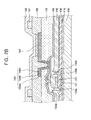
- FIG. 1 is a cross-sectional schematic view of a deposition apparatus having a deposition mask.
- a frame 4 including a mask 1 is positioned at a portion corresponding to a crucible 3 installed in a vacuum chamber 2, and a target 5 (e.g., a pixel defining layer) on which a thin layer will be formed is mounted on the frame 4.
- a magnet unit 6 is driven to closely adhere the mask 1 and frame 4 to the target 5 on which the thin layer will be formed.
- a material contained in the crucible 3 is then deposited on the target 5.
- the surface of the mask 1 may include inconsistencies (or unevenness) of about 2 to 3 ⁇ m.
- the target 5 may be scratched from the inconsistencies in the mask 1.
- a spacer structure is typically formed between the target 5 and the mask 1 in order to prevent damage to the pixel defining layer.
- FIGS. 2A and 2B are cross-sectional schematic views illustrating a method of fabricating a conventional OLED display device.
- a buffer layer 110 is formed on a substrate 100.
- a semiconductor layer including source and drain regions 120a and 120b and a channel region 121 is formed on the buffer layer 110.
- a gate insulating layer 130 is formed on the semiconductor layer, and a gate electrode 131 is formed on the gate insulating layer 130.
- An interlayer insulating layer 140 is formed on the gate insulating layer 130, and source and drain electrodes 150a and 150b are formed on the interlayer insulating layer 140 and electrically connected to the source and drain regions 120a and 120b, respectively, through contact holes.
- the OLED includes a first electrode 180 and a pixel defining layer 190.
- the first electrode 180 is formed on a protective layer 160 and a planarization layer 170, which are, in turn, formed on a thin film transistor (TFT).
- TFT thin film transistor
- the first electrode 180 functions as an anode that is electrically connected to the drain electrode 150b through a via hole.
- the pixel defining layer 190 exposes a region of the first electrode 180, and has an opening defining a pixel.
- a spacer film is coated on the pixel defining layer 190, and a photoresist layer is formed on the spacer film, and exposed and developed using a shadow mask, thereby forming a photoresist pattern. Thereafter, the spacer film is patterned using the photoresist pattern as a mask, forming a spacer pattern 191.
- an organic layer 192 having an EML is formed using the deposition apparatus having the deposition mask, described above with reference to FIG. 1 .
- a second electrode 193 is formed on the organic layer 192 using a sputtering process.
- the spacer pattern prevents or protects the pixel defining layer 190 from being damaged from inconsistencies in the deposition mask.
- the spacer pattern is formed by patterning the spacer film using the photolithography process, a residual layer of the spacer film may remain on the first electrode.
- aspects of embodiments of the present invention are directed toward an organic light emitting diode (OLED) display device and a method of fabricating the same, in which when an organic layer having an emission layer (EML) is formed using a deposition mask, damage to a pixel defining layer due to the unevenness of the deposition mask is prevented or reduced using spherical spacers disposed on the pixel defining layer, so that a conventional photolithography process for forming a spacer pattern is omitted.
- OLED organic light emitting diode
- the first level may be lower than the second level.
- the width of the first region may be at least 1/2 the size of each of the spherical spacers.
- Each of the spherical spacers may have a size of about 3 to 10 ⁇ m.
- a method of fabricating an OLED display device includes: providing a substrate; forming a first electrode on the substrate; forming a pixel defining layer on the first electrode; applying a plurality of spherical spacers on the pixel defining layer; forming an opening in the pixel defining layer partially exposing the first electrode and separated into a first region having a first level and a second region having a second level on the pixel defining layer; forming an organic layer having an emission layer (EML) on the first electrode; and forming a second electrode on the organic layer, wherein the first region is formed along an edge portion of the opening.
- EML emission layer
- the method may further include exposing the pixel defining layer to light to form the opening and the first and second regions in the pixel defining layer.
- the process of exposing the pixel defining layer to light may be performed using a halftone mask.
- the halftone mask includes a light blocking region, a semi-transmissive region, and a transmissive region.
- the opening may correspond to the transmissive region
- the first region may correspond to the semi-transmissive region
- the second region may correspond to the light blocking region.
- the opening may correspond to the light blocking region
- the first region may correspond to the semi-transmissive region
- the second region may correspond to the transmissive region.
- the method may further include baking the substrate with the spherical spacers.
- the baking process may be performed at a temperature of about 50 to 200°C.
- FIG. 1 is a cross-sectional schematic view of a conventional deposition apparatus having a deposition mask
- FIGS. 2A and 2B are cross-sectional schematic views illustrating a method of fabricating a conventional organic light emitting diode (OLED) display device
- FIG. 3 is a plan schematic view of a unit pixel of a general OLED display device
- FIGS. 4A through 4E are cross-sectional schematic views illustrating a method of fabricating an OLED display device according to an exemplary embodiment of the present invention
- FIGS. 5A and 5B are photographs of a resultant structure before and after a developing process is performed without a bake process.
- FIGS. 6A and 6B are photographs of a resultant structure before and after a developing process is performed including a bake process.
- FIG. 3 is a plan schematic view of a unit pixel of a general organic light emitting diode (OLED) display device.
- OLED organic light emitting diode
- the unit pixel includes a switching transistor Tr1, a driving transistor Tr2, a capacitor 40, and an OLED 50.
- a gate line 10, a data line 20, and a power supply line 30 are connected to respective components of the unit pixel.
- the switching transistor Tr1 is driven in response to a scan signal applied to the gate line 10, and functions to transmit a data signal from data line 20 to the driving transistor Tr2.
- the driving transistor Tr2 receives the data signal, receives a signal from the power supply line 30, and determines the amount of current flowing through the OLED 50 based on a gate-source voltage difference.
- the capacitor 40 functions to store the data signal transmitted through the switching transistor Tr1 for each frame.
- FIGS. 4A through 4E are cross-sectional schematic views illustrating a method of fabricating an OLED display device according to an exemplary embodiment of the present invention.
- a buffer layer 210 is formed on the surface of a transparent insulating substrate 200.
- the buffer layer 210 is generally formed by depositing silicon oxide using a plasma-enhanced chemical vapor deposition (PECVD) process.
- PECVD plasma-enhanced chemical vapor deposition
- the buffer layer 210 prevents or protects from the diffusion of impurities into the transparent insulating substrate 200 during crystallization of an amorphous silicon (a-Si) layer formed in a subsequent process.
- a-Si layer as a semiconductor layer is deposited on the buffer layer 210.
- the a-Si layer is crystallized using, for example, an excimer laser annealing (ELA) process, a sequential lateral solidification (SLS) process, a metal induced crystallization (MIC) process, or a metal induced lateral crystallization (MILC) process, and may be patterned using photolithography and etching processes, forming a semiconductor layer pattern.
- ELA excimer laser annealing
- SLS sequential lateral solidification
- MIC metal induced crystallization
- MILC metal induced lateral crystallization
- a gate insulating layer 230 is formed with the semiconductor layer pattern.
- the gate insulating layer 230 may be a silicon oxide (SiO 2 ) layer, a silicon nitride (SiN x ) layer, or a double layer thereof.
- a gate electrode 231 is formed on the gate insulating layer 230 in a region corresponding to a channel region 221 of the semiconductor layer pattern.
- the gate electrode 231 may be formed of, for example, aluminum (Al), an Al alloy, molybdenum (Mo), or an Mo alloy.
- impurity ions are implanted into the semiconductor layer pattern using the gate electrode 231 as an implantation mask, thereby forming source and drain regions 220a and 220b.
- the implantation process may be performed using n+ impurity ions or p+ impurity ions as a dopant.
- the interlayer insulating layer 240 may be a silicon oxide (SiO 2 ) layer, a silicon nitride (SiN x ) layer, or a double layer thereof.
- the interlayer insulating layer 240 and the gate insulating layer 230 are etched using photolithography and etching processes, forming contact holes exposing the source and drain regions 220a and 220b.
- a source/drain electrode material is formed and etched using photolithography and etching processes, forming source and drain electrodes 250a and 250b connected to the source and drain regions 220a and 220b, respectively.
- the source/drain electrode material may be a single layer formed of, for example, Mo, W, MoW, AlNd, Ti, Al, an Al alloy, Ag, or an Ag alloy.
- the source/drain electrode material may be a multilayered structure utilizing a low-resistance material, for example, a stack structure of Mo/Al/Mo, MoW/Al-Nd/MoW, Ti/Al/Ti, Mo/Ag/Mo, or Mo/Ag-alloy/Mo.
- An insulating layer is formed on the source and drain electrodes 250a and 250b.
- the insulating layer may be an inorganic layer 260, an organic layer 270, or a double layer thereof.
- a first electrode 280 is formed on the insulating layer, connecting to the source electrode 250a or the drain electrode 250b through a via hole formed in the insulating layer.
- the first electrode 280 may be embodied as a transparent electrode when the OLED display device is a bottom-emitting type, or embodied as a reflective electrode when the OLED display device is a top-emitting type.
- the first electrode 280 may be formed of, for example, indium tin oxide (ITO), indium zinc oxide (IZO), tin oxide (TO), or zinc oxide (ZnO).
- ITO indium tin oxide
- IZO indium zinc oxide
- TO tin oxide
- ZnO zinc oxide
- the first electrode 280 may be formed by sequentially stacking a reflective layer and a transparent electrode.
- the reflective layer may be formed of, for example, Ag, Mg, Al, Pt, Pd, Au, Ni, Nd, Ir, Cr, or combinations thereof
- the transparent electrode may be formed of, for example, ITO, IZO, TO, or ZnO.
- the first electrode 280 may be formed by, for example, sequentially stacking a lower electrode layer 280a, a reflective electrode layer 280b, and an upper electrode layer 280c.
- the lower electrode 280a may be formed of, for example, ITO, IZO, TO, or ZnO, and may have a thickness of about 50 to 100 ⁇ . When the lower electrode layer 280a has a thickness of less than 50 ⁇ , it may be difficult to form the lower electrode layer 280a to a uniform thickness. When the lower electrode layer 280a has a thickness of more than 100 ⁇ , the adhesion of the lower electrode layer 280a to the reflective electrode layer 280b may weaken due to stress to the lower electrode layer 280a.
- the reflective electrode layer 280b may be formed of, for example, Al, an Al alloy, Ag, or an Ag alloy, and may have a thickness of about 900 to 2000 ⁇ . When the reflective electrode layer 280b has a thickness of less than 900 ⁇ , light may be partially transmitted through the reflective electrode layer 280b.
- the reflective electrode layer 280b should have a thickness of about 1000 ⁇ or more in order to prevent or block the transmission of light. Forming the reflective electrode layer 280b to a thickness of more than 2000 ⁇ may be disadvantageous in terms of fabrication cost and process time.
- the reflective electrode layer 280b functions to reflect light so as to increase luminance and luminous efficiency.
- the upper electrode layer 280c may be formed of, for example, ITO, IZO, TO, or ZnO, and may have a thickness of about 50 to 100 ⁇ . When the upper electrode layer 280c has a thickness of less than 50 ⁇ , it may be difficult to form the upper electrode layer 280c with a uniform thickness. When the upper electrode layer 280c is formed to a thickness of more than 100 ⁇ , the reflectance of a blue region may be reduced up to 15% or more due to an interference effect.
- the pixel defining layer 281 may be formed of, for example, polyacrylates resin, epoxy resin, phenolic resin, polyamides resin, polyimides rein, unsaturated polyesters resin, poly(phenylenethers) resin, poly(phenylenesulfides) resin, or benzocyclobutene (BCB).
- polyacrylates resin epoxy resin, phenolic resin, polyamides resin, polyimides rein, unsaturated polyesters resin, poly(phenylenethers) resin, poly(phenylenesulfides) resin, or benzocyclobutene (BCB).
- the photolithography and etching processes involve exposing the pixel defining layer 281 using a halftone mask 282.
- the halftone mask 282 includes a light blocking region 282a, a semi-transmissive region 282b, and a transmissive region 282c.
- the light blocking region 282a completely blocks light
- the semi-transmissive region 282b partially transmits light
- the transmissive region 282c wholly transmits light.
- the structure of the halftone mask 282 may be varied according to a material of the pixel defining layer 281.
- a portion of the halftone mask 282 where the opening is formed is the transmissive region
- a portion of the halftone mask 282 where the first region having the first level is formed is the semi-transmissive region
- a portion of the halftone mask 282 where the second region having the second level is formed is the light blocking region.
- a portion of the pixel defining layer 281 corresponding to the opening 281 is completely removed, a portion of the pixel defining layer 281 corresponding to the first region is partially removed, and a portion of the pixel defining layer 281 corresponding to the second region is not removed.
- a portion of the halftone mask 282 where the opening will be formed would be the light blocking region
- a portion of the halftone mask 282 where the first region having the first level will be formed would be the semi-transmissive region
- a portion of the halftone mask 282 where the second region having the second level will be formed would be the transmissive region.
- a portion of the pixel defining layer 281, which is irradiated with light through the halftone mask 282 hardens so that an unirradiated portion may be removed during a subsequent developing process.
- a portion of the pixel defining layer 281 corresponding to the opening is completely removed, a portion of the pixel defining layer 281 corresponding to the first region is partially removed, and a portion of the pixel defining layer 281 corresponding to the second region is not removed.
- the pixel defining layer 281 is exposed using the above-described halftone mask 282 so that the opening may be completely removed, the first region having the first level may be partially removed, and the second region having the second level may be preserved during a subsequent developing process. As a result, the first level will be disposed lower than the second level.
- a plurality of spherical spacers 290a are applied onto the pixel defining layer 281.
- Each of the spherical spacers may have a size of about 3 to 10 ⁇ m.
- the spacers may be too small to prevent or protect from damage to the pixel defining layer 281 due to inconsistencies or unevenness of a deposition mask during a subsequent process of depositing an organic layer.
- a second electrode or other layers formed on the pixel defining layer 281 may be unacceptably nonuniform due to the large size of the spherical spacers.
- the spherical spacers 290a may be applied using, for example, a spacer sprayer 290. Although the spherical spacers 290a are illustrated as being sprayed at regular intervals for simplicity, the spherical spacers 290a are generally sprayed nonuniformly in practice.
- a bake process may be performed to fix the spherical spacers 290a to the pixel defining layer 281.
- FIGS. 5A and 5B are photographs of a resultant structure before and after a developing process when a bake process is not performed.
- FIGS. 6A and 6B are photographs of a resultant structure before and after the developing process was performed after a bake process.
- the spherical spacers 290a were disposed on the pixel defining layer 281.
- FIG. 6B after a bake process, the developing process was performed, and the spherical spacers 290a were retained on the pixel defining layer 281.
- spherical spacers 290a are sprayed, and the opening and the first and second regions having the first and second levels are thereafter formed in the pixel defining layer 281 using the developing process.
- the bake process is omitted after the spherical spacers 290a are sprayed, the spherical spacers 290a are lost during the developing process.
- the bake process is performed after the spherical spacers 290a are sprayed, the spherical spacers 290a remain fixed to the surface of the pixel defining layer 281.
- the bake process may be performed at temperatures of about 50 to 200°C.
- the spherical spacers 290a may not be effectively fixed to the pixel defining layer 281.
- a residual layer may remain on the pixel defining layer 281, possibly reducing the effectiveness of a later developing process.
- the pixel defining layer 281 is developed to form an opening 281a and a nonopening in the pixel defining layer 281.
- the opening 281 a exposes a portion of the first electrode 280 and defines an emission region, and the nonopening of the pixel defining layer 281 is divided into a first region having a first level A and a second region having a second level B.
- the formation of the opening 281 a and the first and second regions having the first and second levels A and B includes removing the pixel defining layer 281 where the opening 281 a is formed, and a portion of the pixel defining layer 281 where the first region having the first level is formed, and leaving a portion of the pixel defining layer 281 where the second region having the second level is retained.
- the pixel defining layer 281 is formed of a negative material
- a similar structure is formed by generally irradiating the regions opposite the regions irradiated for the positive material.
- the portion of the pixel defining layer 281 corresponding to the opening 281 a is completely removed, exposing a portion of the first electrode 280 defining a pixel.
- a portion of the pixel defining layer 281 corresponding to the first region having the first level A is partially removed and disposed lower than a portion of the pixel defining layer 281 corresponding to the second region having the second level B.
- the spherical spacers 290a are removed from the portions of the pixel defining layer 281 corresponding to the opening 281 a and the first region having the first level A.
- the spacers 290a formed in the second region having the second level B remain disposed on the pixel defining layer 281, but no spherical spacers are disposed on portions of the first electrode 280 exposed by the opening 281 a and on portions 281 b of the pixel defining layer 281 corresponding to the first region having the first level A.
- the first region having the first level A is formed along an edge portion of the opening 281 a.
- the first region having the first level A is formed so that spherical spacers 290a are not disposed on the edge portion of the opening 281 a.
- the spherical spacers 290a may hinder a subsequent process of depositing an organic layer using a deposition mask, possibly causing a shadow phenomenon.
- an organic layer pattern may be formed to a nonuniform thickness and shape at an edge of the organic layer. Therefore, removal of spherical spacers 290a from the edge of the opening 281 a is generally appropriate.
- the width of the first region having the first level A may be at least 1/2 the size of each of the spherical spacers 290a.
- the width of the first region having the first level A is smaller than 1/2 the size of each of the spherical spacers 290a, it may be more difficult to remove the spacers 290a from the edge portion of the opening 281 a.
- the maximum width of the first region having the first level A may be appropriately controlled considering the width of the second region having the second level B on which the spacers 290a are retained. That is, the maximum width of the first region having the first level A may be controlled to be in the range in which the spherical spacers 290a may be disposed in the second region having the second level B.
- the width of the first region having the first level A may be determined by controlling the width of the semi-transmissive region of the halftone mask 282.
- an organic layer 291 having an emission layer (EML) is formed on the first electrode 280, and a second electrode 292 is formed on the organic layer 291.
- EML emission layer
- the organic layer 291 having the EML is formed by a deposition apparatus using a deposition mask.
- the spherical spacers 290a maintain a spacing between the pixel defining layer 281 and the deposition mask, thereby preventing or reducing damage to the pixel defining layer 281 due to inconsistencies in the deposition mask.
- the pixel defining layer 281 is formed on the first electrode 280.
- the regions where the opening 281 a and the first and second regions having the first and second levels A and B will be formed are exposed using the halftone mask 282.
- the spherical spacers 290a are applied and fixed to the pixel defining layer 281 using a bake process.
- the pixel defining layer 281 is developed such that the spherical spacers 290a are retained on the second region having the second level B of the pixel defining layer 281.
- the spherical spacers 290a are removed from the first region having the first level A.
- the occurrence of a shadow phenomenon which may cause nonuniform formation of the organic layer pattern, can be prevented in edge portions of the organic layer 291 during the formation of the organic layer 291.
- the present embodiment it is unnecessary to perform a photolithography process for forming a spacer pattern. As a result, the degradation of the OLED display device from residual spacer film remaining on a first electrode can be prevented or reduced. In addition, shadow phenomenon caused by nonuniform formation of the organic layer pattern in edge portions of the organic layer 291 can be inhibited.
- the HTL may be formed of a hole transport material, such as N,N'-di(naphthalene-1-yl)-N,N'-diphenyl-benzidine ( ⁇ -NPB) or N,N'-bis(3-methyl phenyl)-N,N'-dipheyl-[1,1'-biphenyl]-4,4'-diamine (TPD).
- ⁇ -NPB N,N'-di(naphthalene-1-yl)-N,N'-diphenyl-benzidine
- TPD N,N'-bis(3-methyl phenyl)-N,N'-dipheyl-[1,1'-biphenyl]-4,4'-diamine
- the HTL may be formed to a thickness of about 10 to 50 nm. When the HTL is formed to a thickness of less than 10 nm or more than 50 nm, the hole transport characteristic of the HTL may be compromised.
- the HTL may further include a dopant that emits light due to a hole-electron combination process.
- the dopant may be, for example, 4-(dicyanomethylene)-2-t-butyl-6-(1,1,7,7-tetramethyljulolidyl-9-enyl)-4H-pyran (DCJTB), Coumarin 6, rubrene, DCM, DCJTB, perylene, or quinacridone.
- the HTL may include 0.1 to 5% by weight of the dopant based on a total weight of the hole transport material.
- the HIL may be formed of a starburst amine compound.
- the HIL may have a thickness of about 30 to 100 nm. When the HIL has a thickness of less than 30 nm or more than 100 nm, the hole injection characteristics of the HIL may be compromised.
- the HIL reduces contact resistance between an opposing electrode and the HTL and improves the hole transport capability of an anode, thereby improving the overall characteristics of the OLED display device.
- the EML may be formed of, for example, 4,4'-bis(carbazol-9-yl)-biphenyl (CBP).
- CBP 4,4'-bis(carbazol-9-yl)-biphenyl
- the present invention is not limited to the material of the EML.
- the EML may further include a dopant that emits light due to a hole-electron combination process.
- the kind and content of the dopant added to an EML may be about the same as those of the dopant added to the HTL.
- the EML may have a thickness of about 10 to 40 nm.
- the ETL may be formed of an electron transport material, such as tris(8-quinolinolate)-aluminium (Alq 3) or Almq 3. Like the HTL, the ETL may further include a dopant that emits light due to a hole-electron combination process. In this case, the kind and content of the dopant added to the ETL may be similar to those of the dopant added to the HTL.
- the ETL may have a thickness of about 30 to 100 nm. When the ETL has a thickness of less than 30 nm or more than 100 nm, the efficiency of the OLED display device may be compromised, and required driving voltages may be increased.
- a hole blocking layer may further be formed between the EML and the ETL.
- the HBL prevents the transport of excitons generated by a phosphorescent material to the ETL or prevents the transport of holes to the ETL.
- the HBL may be formed of, for example, BAlq.
- the EIL may be formed of, for example, LiF to a thickness of about 0.1 to 10 nm. When the EIL has a thickness of less than 0.1 nm or more than 10 nm, required driving voltages may be increased.
- the second electrode 292 formed on the organic layer 291 is embodied as a reflective electrode, which may be formed of, for example, Li, Ca, LiF/Ca, LiF/Al, Al, Mg, or an Mg alloy.
- the second electrode 292 formed on the organic layer 291 is embodied as a semi-transmissive cathode or a stack structure obtained by sequentially stacking a semi-transmissive cathode and a transmissive cathode.
- the semi-transmissive cathode may be formed of, for example, Li, Ca, LiF/Ca, LiF/Al, Mg, or an Mg alloy to a thickness of about 5 to 30 nm.
- the semi-transmissive cathode may be a metal having a low work function, for example, Li, Ca, LiF/Ca, LiF/Al, Al, Mg, or an Mg alloy
- the transmissive cathode may be, formed on the semi-transmissive cathode using a low-resistance layer formed of, for example, indium tin oxide (ITO) or indium zinc oxide (IZO).
- ITO indium tin oxide
- IZO indium zinc oxide
- the transmittance of the second electrode 292 may be markedly reduced.
- the total thickness of the semi-transmissive cathode and the transmissive cathode may range from 10 to 400 nm.
- spherical spacers are formed on the pixel defining layer, to prevent or reduce damage to the pixel defining layer due to inconsistencies or unevenness of the deposition mask. Therefore, a conventional process of forming a spacer pattern is not required.
- the process of forming the spacer pattern is omitted, the number of photolithography processes may be reduced, and material costs may be saved.
- the spherical spacers are removed from edge portions of the opening of the pixel defining layer to prevent the occurrence of a shadow phenomenon caused by nonuniform formation of the organic layer pattern in edge portions of the organic layer.
Landscapes
- Engineering & Computer Science (AREA)
- Manufacturing & Machinery (AREA)
- Microelectronics & Electronic Packaging (AREA)
- Electroluminescent Light Sources (AREA)
Abstract
Description
- The present invention relates to an organic light emitting diode (OLED) display device and a method of fabricating the same.
- In general, an organic light emitting diode (OLED) includes an organic layer interposed between a first electrode (i.e., an anode) and a second electrode (i.e., a cathode). The first electrode is a transparent electrode formed of, for example, indium tin oxide (ITO), and the second electrode is formed of a metal having a low work function, such as Ca, Li, or Al. When a forward voltage is applied to the OLED, holes emitted from the anode combine with electrons emitted from the cathode to form excitons, and while the excitons are making the transition from an excited state to a ground state, light is emitted.
- The first electrode is generally formed as a reflective electrode that reflects light, while the second electrode is generally formed as a transmissive electrode that transmits light. Thus, the OLED may be fabricated so that light is emitted by the organic layer toward the second electrode.
- In this case, the organic layer may be formed by various methods. For example, the organic layer may be formed by a deposition method. Specifically, the deposition of the organic layer includes closely adhering a mask having the same pattern as a thin layer to be formed on an underlying layer, and depositing the thin layer.
-
FIG. 1 is a cross-sectional schematic view of a deposition apparatus having a deposition mask. - Referring to
FIG. 1 , in a method of depositing a thin layer of an OLED display device (i.e., an organic layer having an emission layer (EML)), aframe 4 including amask 1 is positioned at a portion corresponding to acrucible 3 installed in avacuum chamber 2, and a target 5 (e.g., a pixel defining layer) on which a thin layer will be formed is mounted on theframe 4. Amagnet unit 6 is driven to closely adhere themask 1 andframe 4 to thetarget 5 on which the thin layer will be formed. A material contained in thecrucible 3 is then deposited on thetarget 5. - However, the surface of the
mask 1 may include inconsistencies (or unevenness) of about 2 to 3 µm. Thus, when themask 1 is too closely adhered to thetarget 5, thetarget 5 may be scratched from the inconsistencies in themask 1. Accordingly, a spacer structure is typically formed between thetarget 5 and themask 1 in order to prevent damage to the pixel defining layer. -
FIGS. 2A and2B are cross-sectional schematic views illustrating a method of fabricating a conventional OLED display device. - Referring to
FIG. 2A , abuffer layer 110 is formed on asubstrate 100. A semiconductor layer including source anddrain regions channel region 121 is formed on thebuffer layer 110. Agate insulating layer 130 is formed on the semiconductor layer, and agate electrode 131 is formed on thegate insulating layer 130. Aninterlayer insulating layer 140 is formed on thegate insulating layer 130, and source anddrain electrodes interlayer insulating layer 140 and electrically connected to the source anddrain regions - An OLED is then formed. The OLED includes a
first electrode 180 and apixel defining layer 190. Thefirst electrode 180 is formed on aprotective layer 160 and aplanarization layer 170, which are, in turn, formed on a thin film transistor (TFT). Thefirst electrode 180 functions as an anode that is electrically connected to thedrain electrode 150b through a via hole. Thepixel defining layer 190 exposes a region of thefirst electrode 180, and has an opening defining a pixel. - A spacer film is coated on the
pixel defining layer 190, and a photoresist layer is formed on the spacer film, and exposed and developed using a shadow mask, thereby forming a photoresist pattern. Thereafter, the spacer film is patterned using the photoresist pattern as a mask, forming aspacer pattern 191. - Referring to
FIG. 2B , anorganic layer 192 having an EML is formed using the deposition apparatus having the deposition mask, described above with reference toFIG. 1 . Asecond electrode 193 is formed on theorganic layer 192 using a sputtering process. In this case, when theorganic layer 192 is formed using the deposition apparatus, the spacer pattern prevents or protects thepixel defining layer 190 from being damaged from inconsistencies in the deposition mask. - However, in this conventional method of fabricating the OLED display device, an extra photolithography process for forming the spacer pattern is added, and additional material costs for the spacer film are incurred.
- Furthermore, since the spacer pattern is formed by patterning the spacer film using the photolithography process, a residual layer of the spacer film may remain on the first electrode.
- Aspects of embodiments of the present invention are directed toward an organic light emitting diode (OLED) display device and a method of fabricating the same, in which when an organic layer having an emission layer (EML) is formed using a deposition mask, damage to a pixel defining layer due to the unevenness of the deposition mask is prevented or reduced using spherical spacers disposed on the pixel defining layer, so that a conventional photolithography process for forming a spacer pattern is omitted.
- According to an embodiment of the present invention, an OLED display device includes: a substrate; a first electrode on the substrate; a pixel defining layer on the first electrode, the pixel defining layer including an opening exposing the first electrode and a nonopening separated into a first region having a first level, and a second region having a second level; a plurality of spherical spacers on the second region of the pixel defining layer; an organic layer on the first electrode and including an emission layer (EML); and a second electrode on the organic layer, wherein the first region is located along an edge portion of the opening.
- The first level may be lower than the second level.
- The width of the first region may be at least 1/2 the size of each of the spherical spacers.
- Each of the spherical spacers may have a size of about 3 to 10 µm.
- According to another embodiment of the present invention, a method of fabricating an OLED display device includes: providing a substrate; forming a first electrode on the substrate; forming a pixel defining layer on the first electrode; applying a plurality of spherical spacers on the pixel defining layer; forming an opening in the pixel defining layer partially exposing the first electrode and separated into a first region having a first level and a second region having a second level on the pixel defining layer; forming an organic layer having an emission layer (EML) on the first electrode; and forming a second electrode on the organic layer, wherein the first region is formed along an edge portion of the opening.
- After forming the pixel defining layer, the method may further include exposing the pixel defining layer to light to form the opening and the first and second regions in the pixel defining layer.
- The process of exposing the pixel defining layer to light may be performed using a halftone mask.
- The halftone mask includes a light blocking region, a semi-transmissive region, and a transmissive region. When the pixel defining layer is formed of a positive material, the opening may correspond to the transmissive region, the first region may correspond to the semi-transmissive region, and the second region may correspond to the light blocking region. When the pixel defining layer is formed of a negative material, the opening may correspond to the light blocking region, the first region may correspond to the semi-transmissive region, and the second region may correspond to the transmissive region.
- After applying the spherical spacers, the method may further include baking the substrate with the spherical spacers. The baking process may be performed at a temperature of about 50 to 200°C.
- The accompanying drawings, together with the specification, illustrate exemplary embodiments of the present invention, and, together with the description, serve to explain the principles of the present invention.
-
FIG. 1 is a cross-sectional schematic view of a conventional deposition apparatus having a deposition mask; -
FIGS. 2A and2B are cross-sectional schematic views illustrating a method of fabricating a conventional organic light emitting diode (OLED) display device; -
FIG. 3 is a plan schematic view of a unit pixel of a general OLED display device; -
FIGS. 4A through 4E are cross-sectional schematic views illustrating a method of fabricating an OLED display device according to an exemplary embodiment of the present invention; -
FIGS. 5A and 5B are photographs of a resultant structure before and after a developing process is performed without a bake process; and -
FIGS. 6A and 6B are photographs of a resultant structure before and after a developing process is performed including a bake process. - In the following detailed description, only certain exemplary embodiments of the present invention are shown and described, by way of illustration. As those skilled in the art would recognize, the invention may be embodied in many different forms and should not be construed as being limited to the embodiments set forth herein. Furthermore, in the context of the present application, when an element is referred to as being "on" another element, it can be directly on the another element or be indirectly on the another element with one or more intervening elements interposed therebetween. Like reference numerals designate like elements throughout the specification.
-
FIG. 3 is a plan schematic view of a unit pixel of a general organic light emitting diode (OLED) display device. - Referring to
FIG. 3 , the unit pixel includes a switching transistor Tr1, a driving transistor Tr2, acapacitor 40, and anOLED 50. Agate line 10, adata line 20, and apower supply line 30 are connected to respective components of the unit pixel. - The switching transistor Tr1 is driven in response to a scan signal applied to the
gate line 10, and functions to transmit a data signal fromdata line 20 to the driving transistor Tr2. - The driving transistor Tr2 receives the data signal, receives a signal from the
power supply line 30, and determines the amount of current flowing through theOLED 50 based on a gate-source voltage difference. - The
capacitor 40 functions to store the data signal transmitted through the switching transistor Tr1 for each frame. -
FIGS. 4A through 4E are cross-sectional schematic views illustrating a method of fabricating an OLED display device according to an exemplary embodiment of the present invention. - Referring to
FIG. 4A , abuffer layer 210 is formed on the surface of a transparent insulatingsubstrate 200. Thebuffer layer 210 is generally formed by depositing silicon oxide using a plasma-enhanced chemical vapor deposition (PECVD) process. In this case, thebuffer layer 210 prevents or protects from the diffusion of impurities into the transparent insulatingsubstrate 200 during crystallization of an amorphous silicon (a-Si) layer formed in a subsequent process. - An a-Si layer as a semiconductor layer is deposited on the
buffer layer 210. After that, the a-Si layer is crystallized using, for example, an excimer laser annealing (ELA) process, a sequential lateral solidification (SLS) process, a metal induced crystallization (MIC) process, or a metal induced lateral crystallization (MILC) process, and may be patterned using photolithography and etching processes, forming a semiconductor layer pattern. - A
gate insulating layer 230 is formed with the semiconductor layer pattern. In this case, thegate insulating layer 230 may be a silicon oxide (SiO2) layer, a silicon nitride (SiNx) layer, or a double layer thereof. - A
gate electrode 231 is formed on thegate insulating layer 230 in a region corresponding to achannel region 221 of the semiconductor layer pattern. Thegate electrode 231 may be formed of, for example, aluminum (Al), an Al alloy, molybdenum (Mo), or an Mo alloy. - Thereafter, impurity ions are implanted into the semiconductor layer pattern using the
gate electrode 231 as an implantation mask, thereby forming source anddrain regions - Next, an
interlayer insulating layer 240 is formed. The interlayer insulatinglayer 240 may be a silicon oxide (SiO2) layer, a silicon nitride (SiNx) layer, or a double layer thereof. - Thereafter, the
interlayer insulating layer 240 and thegate insulating layer 230 are etched using photolithography and etching processes, forming contact holes exposing the source anddrain regions - A source/drain electrode material is formed and etched using photolithography and etching processes, forming source and
drain electrodes drain regions - An insulating layer is formed on the source and
drain electrodes inorganic layer 260, anorganic layer 270, or a double layer thereof. Afirst electrode 280 is formed on the insulating layer, connecting to thesource electrode 250a or thedrain electrode 250b through a via hole formed in the insulating layer. - The
first electrode 280 may be embodied as a transparent electrode when the OLED display device is a bottom-emitting type, or embodied as a reflective electrode when the OLED display device is a top-emitting type. When thefirst electrode 280 is embodied as a transparent electrode, thefirst electrode 280 may be formed of, for example, indium tin oxide (ITO), indium zinc oxide (IZO), tin oxide (TO), or zinc oxide (ZnO). When thefirst electrode 280 is embodied as a reflective electrode, thefirst electrode 280 may be formed by sequentially stacking a reflective layer and a transparent electrode. In this case, the reflective layer may be formed of, for example, Ag, Mg, Al, Pt, Pd, Au, Ni, Nd, Ir, Cr, or combinations thereof, and the transparent electrode may be formed of, for example, ITO, IZO, TO, or ZnO. - In another embodiment, when the OLED display device is a top-emitting type, the
first electrode 280 may be formed by, for example, sequentially stacking alower electrode layer 280a, areflective electrode layer 280b, and anupper electrode layer 280c. - The
lower electrode 280a may be formed of, for example, ITO, IZO, TO, or ZnO, and may have a thickness of about 50 to 100Å. When thelower electrode layer 280a has a thickness of less than 50Å, it may be difficult to form thelower electrode layer 280a to a uniform thickness. When thelower electrode layer 280a has a thickness of more than 100Å, the adhesion of thelower electrode layer 280a to thereflective electrode layer 280b may weaken due to stress to thelower electrode layer 280a. - The
reflective electrode layer 280b may be formed of, for example, Al, an Al alloy, Ag, or an Ag alloy, and may have a thickness of about 900 to 2000Å. When thereflective electrode layer 280b has a thickness of less than 900Å, light may be partially transmitted through thereflective electrode layer 280b. Thereflective electrode layer 280b should have a thickness of about 1000Å or more in order to prevent or block the transmission of light. Forming thereflective electrode layer 280b to a thickness of more than 2000Å may be disadvantageous in terms of fabrication cost and process time. - The
reflective electrode layer 280b functions to reflect light so as to increase luminance and luminous efficiency. - The
upper electrode layer 280c may be formed of, for example, ITO, IZO, TO, or ZnO, and may have a thickness of about 50 to 100Å. When theupper electrode layer 280c has a thickness of less than 50Å, it may be difficult to form theupper electrode layer 280c with a uniform thickness. When theupper electrode layer 280c is formed to a thickness of more than 100Å, the reflectance of a blue region may be reduced up to 15% or more due to an interference effect. - Thereafter, an insulating layer is formed on the
first electrode 280. In this case, the insulating layer may be apixel defining layer 281. - The
pixel defining layer 281 may be formed of, for example, polyacrylates resin, epoxy resin, phenolic resin, polyamides resin, polyimides rein, unsaturated polyesters resin, poly(phenylenethers) resin, poly(phenylenesulfides) resin, or benzocyclobutene (BCB). - The
pixel defining layer 281 may be formed of a positive material or a negative material. - A portion of a positive material irradiated with light softens during a photolithography process, so that the irradiated portion may be removed during a developing process. Conversely, a portion of negative material, irradiated with light hardens during a photolithography process so that an unirradiated portion may be removed during a developing process.
- Thereafter, photolithography and etching processes are performed to develop an opening and nonopening in the
pixel defining layer 281. The opening partially exposes thefirst electrode 280, and the nonopening is separated into a first region having a first level and a second region having a second level. - Referring to
FIG. 4B , the photolithography and etching processes involve exposing thepixel defining layer 281 using ahalftone mask 282. - The
halftone mask 282 includes alight blocking region 282a, asemi-transmissive region 282b, and atransmissive region 282c. Thelight blocking region 282a completely blocks light, thesemi-transmissive region 282b partially transmits light, and thetransmissive region 282c wholly transmits light. - In this case, the structure of the
halftone mask 282 may be varied according to a material of thepixel defining layer 281. - Specifically, referring to
FIG. 4B , when thepixel defining layer 281 is formed of a positive material, a portion of thehalftone mask 282 where the opening is formed is the transmissive region, a portion of thehalftone mask 282 where the first region having the first level is formed is the semi-transmissive region, and a portion of thehalftone mask 282 where the second region having the second level is formed is the light blocking region. Thus, a portion of thepixel defining layer 281, which is irradiated with light through thehalftone mask 282, softens so that the irradiated portion may be removed during a subsequent developing process. Accordingly, a portion of thepixel defining layer 281 corresponding to theopening 281 is completely removed, a portion of thepixel defining layer 281 corresponding to the first region is partially removed, and a portion of thepixel defining layer 281 corresponding to the second region is not removed. - Although not shown in the drawings, when the
pixel defining layer 281 is a negative material, a portion of thehalftone mask 282 where the opening will be formed would be the light blocking region, a portion of thehalftone mask 282 where the first region having the first level will be formed would be the semi-transmissive region, and a portion of thehalftone mask 282 where the second region having the second level will be formed would be the transmissive region. Thus, a portion of thepixel defining layer 281, which is irradiated with light through thehalftone mask 282, hardens so that an unirradiated portion may be removed during a subsequent developing process. Accordingly, a portion of thepixel defining layer 281 corresponding to the opening is completely removed, a portion of thepixel defining layer 281 corresponding to the first region is partially removed, and a portion of thepixel defining layer 281 corresponding to the second region is not removed. - Accordingly, the
pixel defining layer 281 is exposed using the above-describedhalftone mask 282 so that the opening may be completely removed, the first region having the first level may be partially removed, and the second region having the second level may be preserved during a subsequent developing process. As a result, the first level will be disposed lower than the second level. - Referring to
FIG. 4C , after thepixel defining layer 281 is exposed using thehalftone mask 282, a plurality ofspherical spacers 290a are applied onto thepixel defining layer 281. - Each of the spherical spacers may have a size of about 3 to 10 µm. When each of the spherical spacers has a size of less than 3 µm, the spacers may be too small to prevent or protect from damage to the
pixel defining layer 281 due to inconsistencies or unevenness of a deposition mask during a subsequent process of depositing an organic layer. When each of the spherical spacers has a size of more than 10 µm, a second electrode or other layers formed on thepixel defining layer 281 may be unacceptably nonuniform due to the large size of the spherical spacers. - The
spherical spacers 290a may be applied using, for example, aspacer sprayer 290. Although thespherical spacers 290a are illustrated as being sprayed at regular intervals for simplicity, thespherical spacers 290a are generally sprayed nonuniformly in practice. - After the
spherical spacers 290a are applied, a bake process may be performed to fix thespherical spacers 290a to thepixel defining layer 281. -
FIGS. 5A and 5B are photographs of a resultant structure before and after a developing process when a bake process is not performed. - Referring to
FIG. 5A , before the developing processspherical spacers 290a were disposed on apixel defining layer 281. However, as shown inFIG. 5B , after the developing process thespherical spacers 290a were lost from the surface of thepixel defining layer 281. -
FIGS. 6A and 6B are photographs of a resultant structure before and after the developing process was performed after a bake process. - Referring to
FIG. 6A , before the developing process, thespherical spacers 290a were disposed on thepixel defining layer 281. Referring toFIG. 6B , after a bake process, the developing process was performed, and thespherical spacers 290a were retained on thepixel defining layer 281. - According to an embodiment of the present invention, after the
pixel defining layer 281 is exposed using thehalftone mask 282,spherical spacers 290a are sprayed, and the opening and the first and second regions having the first and second levels are thereafter formed in thepixel defining layer 281 using the developing process. In this case, when the bake process is omitted after thespherical spacers 290a are sprayed, thespherical spacers 290a are lost during the developing process. When the bake process is performed after thespherical spacers 290a are sprayed, thespherical spacers 290a remain fixed to the surface of thepixel defining layer 281. - The bake process may be performed at temperatures of about 50 to 200°C. When the bake process is performed at temperatures below 50°C, the
spherical spacers 290a may not be effectively fixed to thepixel defining layer 281. When the bake process is performed at temperatures above 200°C, a residual layer may remain on thepixel defining layer 281, possibly reducing the effectiveness of a later developing process. - Referring to
FIG. 4D , after the bake process is performed, thepixel defining layer 281 is developed to form anopening 281a and a nonopening in thepixel defining layer 281. The opening 281 a exposes a portion of thefirst electrode 280 and defines an emission region, and the nonopening of thepixel defining layer 281 is divided into a first region having a first level A and a second region having a second level B. - As described above, when the
pixel defining layer 281 is formed of a positive material, the formation of the opening 281 a and the first and second regions having the first and second levels A and B includes removing thepixel defining layer 281 where the opening 281 a is formed, and a portion of thepixel defining layer 281 where the first region having the first level is formed, and leaving a portion of thepixel defining layer 281 where the second region having the second level is retained. - When the
pixel defining layer 281 is formed of a negative material, a similar structure is formed by generally irradiating the regions opposite the regions irradiated for the positive material. - In this case, the portion of the
pixel defining layer 281 corresponding to theopening 281 a is completely removed, exposing a portion of thefirst electrode 280 defining a pixel. A portion of thepixel defining layer 281 corresponding to the first region having the first level A is partially removed and disposed lower than a portion of thepixel defining layer 281 corresponding to the second region having the second level B. - During the removal of the portions of the
pixel defining layer 281 corresponding to theopening 281 a and the first region having the first level A, thespherical spacers 290a are removed from the portions of thepixel defining layer 281 corresponding to theopening 281 a and the first region having the first level A. Thus, thespacers 290a formed in the second region having the second level B remain disposed on thepixel defining layer 281, but no spherical spacers are disposed on portions of thefirst electrode 280 exposed by the opening 281 a and onportions 281 b of thepixel defining layer 281 corresponding to the first region having the first level A. - In this case, the first region having the first level A is formed along an edge portion of the opening 281 a.
- In the present embodiment, the first region having the first level A is formed so that
spherical spacers 290a are not disposed on the edge portion of the opening 281 a. - If
spherical spacers 290a are disposed on the edge portion of the opening 281 a, thespherical spacers 290a may hinder a subsequent process of depositing an organic layer using a deposition mask, possibly causing a shadow phenomenon. In other words, an organic layer pattern may be formed to a nonuniform thickness and shape at an edge of the organic layer. Therefore, removal ofspherical spacers 290a from the edge of the opening 281 a is generally appropriate. - In this case, the width of the first region having the first level A may be at least 1/2 the size of each of the
spherical spacers 290a. When the width of the first region having the first level A is smaller than 1/2 the size of each of thespherical spacers 290a, it may be more difficult to remove thespacers 290a from the edge portion of the opening 281 a. - Also, the maximum width of the first region having the first level A may be appropriately controlled considering the width of the second region having the second level B on which the
spacers 290a are retained. That is, the maximum width of the first region having the first level A may be controlled to be in the range in which thespherical spacers 290a may be disposed in the second region having the second level B. - In this case, the width of the first region having the first level A may be determined by controlling the width of the semi-transmissive region of the
halftone mask 282. - Referring to
FIG. 4E , anorganic layer 291 having an emission layer (EML) is formed on thefirst electrode 280, and asecond electrode 292 is formed on theorganic layer 291. - The
organic layer 291 having the EML is formed by a deposition apparatus using a deposition mask. In this case, when theorganic layer 291 is formed using the deposition apparatus, even if the deposition mask is closely adhered to thesubstrate 200 having thepixel defining layer 281, thespherical spacers 290a maintain a spacing between thepixel defining layer 281 and the deposition mask, thereby preventing or reducing damage to thepixel defining layer 281 due to inconsistencies in the deposition mask. - In the above-described method of fabricating the OLED display device according to the present embodiment, the
pixel defining layer 281 is formed on thefirst electrode 280. The regions where the opening 281 a and the first and second regions having the first and second levels A and B will be formed are exposed using thehalftone mask 282. Thereafter, thespherical spacers 290a are applied and fixed to thepixel defining layer 281 using a bake process. Thepixel defining layer 281 is developed such that thespherical spacers 290a are retained on the second region having the second level B of thepixel defining layer 281. As a result, damage to thepixel defining layer 281 due to inconsistencies in the deposition mask during deposition oforganic layer 291 can be prevented or reduced. - Also, the
spherical spacers 290a are removed from the first region having the first level A. Thus, the occurrence of a shadow phenomenon, which may cause nonuniform formation of the organic layer pattern, can be prevented in edge portions of theorganic layer 291 during the formation of theorganic layer 291. - Accordingly, unlike in the conventional method of fabricating the OLED display device, according to the present embodiment, it is unnecessary to perform a photolithography process for forming a spacer pattern. As a result, the degradation of the OLED display device from residual spacer film remaining on a first electrode can be prevented or reduced. In addition, shadow phenomenon caused by nonuniform formation of the organic layer pattern in edge portions of the
organic layer 291 can be inhibited. - The
organic layer 291 includes the EML and may further include, for example, a hole injection layer (HIL), a hole transport layer (HTL), an electron transport layer (ETL), or an electron injection layer (EIL). The present invention is not limited to the construction and material of theorganic layer 291. - The HTL may be formed of a hole transport material, such as N,N'-di(naphthalene-1-yl)-N,N'-diphenyl-benzidine (α-NPB) or N,N'-bis(3-methyl phenyl)-N,N'-dipheyl-[1,1'-biphenyl]-4,4'-diamine (TPD). The HTL may be formed to a thickness of about 10 to 50 nm. When the HTL is formed to a thickness of less than 10 nm or more than 50 nm, the hole transport characteristic of the HTL may be compromised.
- The HTL may further include a dopant that emits light due to a hole-electron combination process. The dopant may be, for example, 4-(dicyanomethylene)-2-t-butyl-6-(1,1,7,7-tetramethyljulolidyl-9-enyl)-4H-pyran (DCJTB),
Coumarin 6, rubrene, DCM, DCJTB, perylene, or quinacridone.
The HTL may include 0.1 to 5% by weight of the dopant based on a total weight of the hole transport material. When the dopant is added to the HTL, the color of light emitted by the EML may be controlled according to the kind and content of the dopant, and the thermal stability of the HTL may be improved to increase the lifetime of the OLED display device. - The HIL may be formed of a starburst amine compound. The HIL may have a thickness of about 30 to 100 nm. When the HIL has a thickness of less than 30 nm or more than 100 nm, the hole injection characteristics of the HIL may be compromised. The HIL reduces contact resistance between an opposing electrode and the HTL and improves the hole transport capability of an anode, thereby improving the overall characteristics of the OLED display device.
- The EML may be formed of, for example, 4,4'-bis(carbazol-9-yl)-biphenyl (CBP). However, the present invention is not limited to the material of the EML.
- Like the HTL, the EML may further include a dopant that emits light due to a hole-electron combination process. In this case, the kind and content of the dopant added to an EML may be about the same as those of the dopant added to the HTL. The EML may have a thickness of about 10 to 40 nm.
- The ETL may be formed of an electron transport material, such as tris(8-quinolinolate)-aluminium (Alq 3) or
Almq 3. Like the HTL, the ETL may further include a dopant that emits light due to a hole-electron combination process. In this case, the kind and content of the dopant added to the ETL may be similar to those of the dopant added to the HTL. The ETL may have a thickness of about 30 to 100 nm. When the ETL has a thickness of less than 30 nm or more than 100 nm, the efficiency of the OLED display device may be compromised, and required driving voltages may be increased. - A hole blocking layer (HBL) may further be formed between the EML and the ETL. The HBL prevents the transport of excitons generated by a phosphorescent material to the ETL or prevents the transport of holes to the ETL. The HBL may be formed of, for example, BAlq.
- The EIL may be formed of, for example, LiF to a thickness of about 0.1 to 10 nm. When the EIL has a thickness of less than 0.1 nm or more than 10 nm, required driving voltages may be increased.
- When the OLED display device is a bottom-emitting type, the
second electrode 292 formed on theorganic layer 291 is embodied as a reflective electrode, which may be formed of, for example, Li, Ca, LiF/Ca, LiF/Al, Al, Mg, or an Mg alloy. - When the OLED display device is a top-emitting type, the
second electrode 292 formed on theorganic layer 291 is embodied as a semi-transmissive cathode or a stack structure obtained by sequentially stacking a semi-transmissive cathode and a transmissive cathode. The semi-transmissive cathode may be formed of, for example, Li, Ca, LiF/Ca, LiF/Al, Mg, or an Mg alloy to a thickness of about 5 to 30 nm. When thesecond electrode 292 is a stack structure, the semi-transmissive cathode may be a metal having a low work function, for example, Li, Ca, LiF/Ca, LiF/Al, Al, Mg, or an Mg alloy, and the transmissive cathode may be, formed on the semi-transmissive cathode using a low-resistance layer formed of, for example, indium tin oxide (ITO) or indium zinc oxide (IZO). In this case, when the semi-transmissive cathode has a thickness of less than 5 nm, electrons may not be injected at a low voltage. Also, when the semi-transmissive cathode has a thickness of more than 30 nm, the transmittance of thesecond electrode 292 may be markedly reduced. The total thickness of the semi-transmissive cathode and the transmissive cathode may range from 10 to 400 nm. - According to an embodiment of the present invention as described above, when the organic layer having the EML is formed using a deposition mask, spherical spacers are formed on the pixel defining layer, to prevent or reduce damage to the pixel defining layer due to inconsistencies or unevenness of the deposition mask. Therefore, a conventional process of forming a spacer pattern is not required.
- Since the process of forming the spacer pattern is omitted, the number of photolithography processes may be reduced, and material costs may be saved.
- Furthermore, since a process of patterning spacer film is eliminated, a residual layer of the spacer film is not left on the first electrode, preventing degradation of the OLED display device.
- Moreover, the spherical spacers are removed from edge portions of the opening of the pixel defining layer to prevent the occurrence of a shadow phenomenon caused by nonuniform formation of the organic layer pattern in edge portions of the organic layer.
Claims (17)
- An organic light emitting diode (OLED) display device comprising:a substrate (200);a first electrode (280) on the substrate (280);a pixel defining layer (281) on the first electrode (280), the pixel defining layer (281) including an opening (281a) exposing the first electrode (280) and a nonopening separated into a first region having a first level (A) and a second region having a second level (B);a plurality of spherical spacers (290a) on the second region of the pixel defining layer (281);an organic layer (291) on the first electrode (280) and including an emission layer (EML); anda second electrode (292) on the organic layer (291),wherein the first region is located along an edge portion (281b) of the opening (281a).
- The OLED display device according to claim 1, wherein the first level (A) is lower than the second level (B).
- The OLED display device according to anyone of claims 1 or 2, wherein the first region has a width at least 1/2 the size of each of the spherical spacers (290a).
- The OLED display device according to anyone of claims 1 to 3, wherein each of the spherical spacers (290a) has a size of about 3 to 10 µm.
- The OLED display device according to anyone of claims 1 to 4, wherein the pixel defining layer (281) comprises a material selected from the group consisting of polyacrylates resin, epoxy resin, phenolic resin, polyamides resin, polyimides resin, unsaturated polyesters resin, poly(phenylenethers) resin, poly(phenylenesulfides) resin, benzocyclobutene (BCB), and combinations thereof.
- The OLED display device according to anyone of claims 1 to 5, wherein the first electrode (280) comprises a material selected from the group consisting of indium tin oxide (ITO), indium zinc oxide (IZO), tin oxide (TO), zinc oxide (ZnO), and combinations thereof, and the second electrode (292) comprises a material selected from the group consisting of Li, Ca, LiF/Ca, LiF/Al, Al, Mg, and combinations thereof.
- The OLED display device according to anyone of claims 1 to 6, wherein the first electrode (280) includes a reflective layer (280b) and a transparent electrode on the reflective layer (280b), the reflective layer (280b) comprising a material selected from the group consisting of Ag, Mg, Al, Pt, Pd, Au, Ni, Nd, Ir, Cr, and combinations thereof, and the transparent electrode comprising a material selected from the group consisting of ITO, IZO, TO, and ZnO; and wherein the second electrode (292) comprises a material selected from the group consisting of Li, Ca, LiF/Ca, LiF/Al, Al, Mg, and an Mg alloy.
- The OLED display device according to anyone of claims 1 to 7, wherein the first electrode (280) includes a lower electrode (280a), a reflective electrode (280b) on the lower electrode (280a), and an upper electrode (280c) on the reflective electrode (280b), the lower electrode (280a) comprising a material selected from the group consisting of ITO, IZO, TO, and ZnO, the reflective electrode (280b) comprising a material selected from the group consisting of Ag, Mg, Al, Pt, Pd, Au, Ni, Nd, Ir, Cr, and combinations thereof, and the upper electrode (280c) comprising a material selected from the group consisting of ITO, IZO, TO, and ZnO; and wherein the second electrode (292) comprises a material selected from the group consisting of Li, Ca, LiF/Ca, LiF/Al, Al, Mg, and an Mg alloy.
- The OLED display device according to anyone of claims 1 to 8, further comprising a thin film transistor (TFT) on the substrate, the TFT including a semiconductor layer having source and drain regions, and source and drain electrodes electrically connected to the source and drain regions of the semiconductor layer, wherein the first electrode (280) is connected to one of the source and drain electrodes.
- A method of fabricating an organic light emitting diode (OLED) display device, comprising:providing a substrate (200);forming a first electrode (280) on the substrate (200);forming a pixel defining layer (281) on the first electrode (280);applying a plurality of spherical spacers (290a) on the pixel defining layer (281);forming an opening (281 a) in the pixel defining layer (281) partially exposing the first electrode (280) and an nonopening separated into a first region having a first level (A) and a second region having a second level (B) on the pixel defining layer (281);forming an organic layer (291) having an emission layer (EML) on the first electrode (280); andforming a second electrode (292) on the organic layer (291),wherein the first region is formed along an edge portion (281 b) of the opening (281 a).
- The method according to claim 10, further comprising, after forming the pixel defining layer (281), exposing the pixel defining layer (281) to light to form the opening (281 a) and the first and second regions in the pixel defining layer (281).
- The method according to anyone of claims 10 or 11, wherein the exposing the pixel defining layer (281) to light is performed by utilizing a halftone mask (282).
- The method according to claim 12, wherein the halftone mask (282) includes a light blocking region (282a), a semi-transmissive region (282b), and a transmissive region (282c), and
wherein when the pixel defining layer (281) is formed of a positive material, the opening (281a) corresponds to the transmissive region (282c), the first region corresponds to the semi-transmissive region (282b), and the second region corresponds to the light blocking region (282a). - The method according to claim 12, wherein the halftone mask (282) includes a light blocking region (282a), a semi-transmissive region (282b), and a transmissive region (282c), and
wherein when the pixel defining layer (281) is formed of a negative material, the opening (281a) corresponds to the light blocking region (282a), the first region corresponds to the semi-transmissive region (282b), and the second region corresponds to the transmissive region (282c). - The method according to anyone of claims 10 to 14, further comprising, after applying the spherical spacers (290a), baking the substrate with the spherical spacers (290a).
- The method according to claim 15, wherein the baking the substrate includes exposing the substrate to temperatures of about 50 to 200°C.
- The method according to anyone of claims 10 to 16, further comprising forming a thin film transistor (TFT) including a semiconductor layer having source and drain regions and source and drain electrodes electrically connected to the source and drain regions of the semiconductor layer, wherein the first electrode (280) is connected to one of the source and drain electrodes.
Applications Claiming Priority (1)
| Application Number | Priority Date | Filing Date | Title |
|---|---|---|---|
| KR1020080010244A KR100924137B1 (en) | 2008-01-31 | 2008-01-31 | Organic Light Emitting Diode Display and method for fabricating of the same |
Publications (2)
| Publication Number | Publication Date |
|---|---|
| EP2086007A1 true EP2086007A1 (en) | 2009-08-05 |
| EP2086007B1 EP2086007B1 (en) | 2014-08-13 |
Family
ID=40491004
Family Applications (1)
| Application Number | Title | Priority Date | Filing Date |
|---|---|---|---|
| EP09150625.3A Ceased EP2086007B1 (en) | 2008-01-31 | 2009-01-15 | Organic light emitting diode display device and method of fabricating the same |
Country Status (5)
| Country | Link |
|---|---|
| US (1) | US8039839B2 (en) |
| EP (1) | EP2086007B1 (en) |
| JP (1) | JP2009182320A (en) |
| KR (1) | KR100924137B1 (en) |
| CN (1) | CN101556991B (en) |
Cited By (2)
| Publication number | Priority date | Publication date | Assignee | Title |
|---|---|---|---|---|
| EP2522700A1 (en) | 2011-05-11 | 2012-11-14 | Saint-Gobain Glass France | Water soluble printing paste |
| CN104218050A (en) * | 2013-06-04 | 2014-12-17 | 三星显示有限公司 | Organic light-emitting display apparatus and method for manufacturing the same |
Families Citing this family (33)
| Publication number | Priority date | Publication date | Assignee | Title |
|---|---|---|---|---|
| KR101084177B1 (en) | 2009-11-30 | 2011-11-17 | 삼성모바일디스플레이주식회사 | OLED display apparatus and Method thereof |
| KR101595471B1 (en) * | 2009-12-11 | 2016-02-18 | 엘지디스플레이 주식회사 | Organic Electroluminescence Device and Method for fabricating the same |
| KR101119046B1 (en) | 2010-01-08 | 2012-03-02 | 삼성모바일디스플레이주식회사 | Organic light emitting display deviece and the fabricating method of the same |
| KR101084193B1 (en) * | 2010-02-16 | 2011-11-17 | 삼성모바일디스플레이주식회사 | An organic light emitting display device and the manufacturing method thereof |
| KR101097346B1 (en) | 2010-03-10 | 2011-12-23 | 삼성모바일디스플레이주식회사 | Organic light emitting display device |
| KR101821167B1 (en) * | 2011-08-30 | 2018-01-24 | 삼성디스플레이 주식회사 | Organic light emitting display device having a reflection structure and method of manufacturing an organic light emitting display device having a reflection structure |
| WO2013032303A2 (en) * | 2011-09-02 | 2013-03-07 | 주식회사 엘엠에스 | Organic electronic device |
| KR101615332B1 (en) | 2012-03-06 | 2016-04-26 | 삼성디스플레이 주식회사 | Pixel arrangement structure for organic light emitting display device |
| KR101927848B1 (en) * | 2012-09-17 | 2018-12-12 | 삼성디스플레이 주식회사 | Organic electroluminescent display and method of manufacturing the same |
| KR101433589B1 (en) * | 2012-12-19 | 2014-08-25 | 엘지디스플레이 주식회사 | Organic Light Emitting Display Device and Method for Manufacturing The Same |
| JP2014145857A (en) * | 2013-01-28 | 2014-08-14 | Sony Corp | Display device and method of manufacturing the same, and electronic equipment |
| KR102055683B1 (en) * | 2013-03-29 | 2019-12-16 | 삼성디스플레이 주식회사 | Organic light emitting display apparatus |
| KR20140139304A (en) * | 2013-05-27 | 2014-12-05 | 삼성디스플레이 주식회사 | Organic light emitting diode display |
| KR102054850B1 (en) * | 2013-05-30 | 2019-12-12 | 삼성디스플레이 주식회사 | Organic light emitting display apparatus and method of manufacturing the same |
| KR102036328B1 (en) | 2013-06-07 | 2019-10-25 | 삼성디스플레이 주식회사 | Organic luminescence emitting display device and method for manufacturing the same |
| KR102090710B1 (en) * | 2013-06-26 | 2020-03-19 | 삼성디스플레이 주식회사 | Thin film transistor substrate, organic light emitting apparatus comprising the same, method for manufacturing thin film transistor substrate, and method for manufacturing organic light emitting apparatus |
| KR102280777B1 (en) | 2013-12-20 | 2021-07-23 | 삼성디스플레이 주식회사 | Display device and manufacturing method thereof |
| KR102283853B1 (en) * | 2013-12-24 | 2021-07-29 | 엘지디스플레이 주식회사 | Organic Light Emitting Display Device and Method for fabricating the thereof |
| US9691835B2 (en) | 2013-12-24 | 2017-06-27 | Boe Technology Group Co., Ltd. | Double-face display panel |
| CN104752461B (en) * | 2013-12-25 | 2018-09-04 | 昆山国显光电有限公司 | A kind of double-side display device and preparation method thereof |
| KR102122402B1 (en) * | 2013-12-31 | 2020-06-15 | 엘지디스플레이 주식회사 | COT Structure Liquid Crystal Display Device and method of fabricating the same |
| KR102160417B1 (en) * | 2014-02-28 | 2020-10-05 | 삼성디스플레이 주식회사 | Organic light emitting display device and manufacturing method thereof |
| JP6371094B2 (en) | 2014-03-31 | 2018-08-08 | 株式会社ジャパンディスプレイ | Organic EL display device |
| US9508778B2 (en) * | 2014-04-25 | 2016-11-29 | Samsung Display Co., Ltd. | Organic light emitting diode display |
| CN104393023B (en) | 2014-12-01 | 2018-01-26 | 京东方科技集团股份有限公司 | A kind of array base palte and preparation method thereof, display device |
| KR102337889B1 (en) * | 2015-02-16 | 2021-12-10 | 삼성디스플레이 주식회사 | Display device |
| KR102362091B1 (en) * | 2015-03-19 | 2022-02-11 | 삼성디스플레이 주식회사 | Display device, optical mask and manufacturing of display device usinh the same |
| CN105448957B (en) * | 2016-01-04 | 2018-06-05 | 京东方科技集团股份有限公司 | Organic electroluminescent display substrate and preparation method thereof, display device |
| CN106384744B (en) * | 2016-11-16 | 2020-04-03 | 信利(惠州)智能显示有限公司 | Method for manufacturing organic light emitting display device |
| KR101989086B1 (en) * | 2017-01-25 | 2019-06-14 | 한국생산기술연구원 | Oled lighting element and method for manufacturing the same |
| CN107579098B (en) * | 2017-08-21 | 2020-05-12 | 上海天马微电子有限公司 | Array substrate and display device |
| KR20220029012A (en) * | 2020-09-01 | 2022-03-08 | 엘지디스플레이 주식회사 | Display device |
| US12089449B2 (en) | 2020-09-29 | 2024-09-10 | Boe Technology Group Co., Ltd. | Display panel and display apparatus |
Citations (4)
| Publication number | Priority date | Publication date | Assignee | Title |
|---|---|---|---|---|
| US20040119419A1 (en) * | 2002-12-11 | 2004-06-24 | Kazuhiko Kai | Organic EL display device |
| US20060097263A1 (en) * | 2004-11-11 | 2006-05-11 | Lee Jeong-Yeol | Organic electroluminescent display device |
| US20070190673A1 (en) * | 2006-02-11 | 2007-08-16 | Ko Ick-Hwan | Organic light emitting diode and method of manufacturing the same |
| KR100796618B1 (en) * | 2007-01-04 | 2008-01-22 | 삼성에스디아이 주식회사 | Organic light emitting diode display and method for fabricating of the same |
Family Cites Families (19)
| Publication number | Priority date | Publication date | Assignee | Title |
|---|---|---|---|---|
| JP2822882B2 (en) | 1994-03-30 | 1998-11-11 | 日本電気株式会社 | Liquid crystal display device and method of manufacturing the same |
| TWI222839B (en) * | 1999-12-17 | 2004-10-21 | Osram Opto Semiconductors Gmbh | Method for encapsulation of electronic devices |
| US7394153B2 (en) * | 1999-12-17 | 2008-07-01 | Osram Opto Semiconductors Gmbh | Encapsulation of electronic devices |
| JP3481232B2 (en) * | 2002-03-05 | 2003-12-22 | 三洋電機株式会社 | Manufacturing method of organic electroluminescence panel |
| KR100898780B1 (en) | 2002-04-19 | 2009-05-20 | 엘지디스플레이 주식회사 | Liquid crystal display device |
| JP2003347041A (en) | 2002-05-22 | 2003-12-05 | Casio Comput Co Ltd | Luminescent panel and its manufacturing method |
| JP2004047458A (en) | 2002-05-24 | 2004-02-12 | Sanyo Electric Co Ltd | Electroluminescence display |
| JP2005011793A (en) | 2003-05-29 | 2005-01-13 | Sony Corp | Manufacturing method of structure of lamination, lamination structure, display element and display device |
| KR100544133B1 (en) * | 2003-09-25 | 2006-01-23 | 삼성에스디아이 주식회사 | Active addressing flat panel display |
| JP4556566B2 (en) * | 2003-11-11 | 2010-10-06 | セイコーエプソン株式会社 | Electro-optical device and electronic apparatus |
| JP2005322564A (en) * | 2004-05-11 | 2005-11-17 | Sony Corp | Manufacturing method of display device, and display device |
| KR100573154B1 (en) * | 2004-06-26 | 2006-04-24 | 삼성에스디아이 주식회사 | Electroluminescence display device and method for manufacturing the same |
| KR20060004476A (en) | 2004-07-09 | 2006-01-12 | 비오이 하이디스 테크놀로지 주식회사 | Method of spacer sprinkling |
| US7753751B2 (en) | 2004-09-29 | 2010-07-13 | Semiconductor Energy Laboratory Co., Ltd. | Method of fabricating the display device |
| JP4879541B2 (en) * | 2004-09-29 | 2012-02-22 | 株式会社半導体エネルギー研究所 | Method for manufacturing display device |
| KR100745332B1 (en) | 2005-09-28 | 2007-08-02 | 삼성에스디아이 주식회사 | Organic light emitting display and method for fabricating the same |
| JP2007128688A (en) * | 2005-11-01 | 2007-05-24 | Toshiba Matsushita Display Technology Co Ltd | Display device and manufacturing method of the same |
| KR100708734B1 (en) | 2005-11-30 | 2007-04-17 | 삼성에스디아이 주식회사 | Organic light emitting display apparatus and method of manufacturing the same |
| KR100793546B1 (en) | 2007-01-03 | 2008-01-14 | 삼성에스디아이 주식회사 | Organic light emitting display device and method for fabricating the same |
-
2008
- 2008-01-31 KR KR1020080010244A patent/KR100924137B1/en not_active IP Right Cessation
- 2008-10-10 JP JP2008263993A patent/JP2009182320A/en active Pending
-
2009
- 2009-01-15 EP EP09150625.3A patent/EP2086007B1/en not_active Ceased
- 2009-01-22 CN CN2009100059697A patent/CN101556991B/en not_active Expired - Fee Related
- 2009-01-23 US US12/321,747 patent/US8039839B2/en active Active
Patent Citations (5)
| Publication number | Priority date | Publication date | Assignee | Title |
|---|---|---|---|---|
| US20040119419A1 (en) * | 2002-12-11 | 2004-06-24 | Kazuhiko Kai | Organic EL display device |
| US20060097263A1 (en) * | 2004-11-11 | 2006-05-11 | Lee Jeong-Yeol | Organic electroluminescent display device |
| US20070190673A1 (en) * | 2006-02-11 | 2007-08-16 | Ko Ick-Hwan | Organic light emitting diode and method of manufacturing the same |
| KR100796618B1 (en) * | 2007-01-04 | 2008-01-22 | 삼성에스디아이 주식회사 | Organic light emitting diode display and method for fabricating of the same |
| EP1942526A2 (en) * | 2007-01-04 | 2008-07-09 | Samsung SDI Co., Ltd. | Organic light emitting diode display device and method of fabricating the same |
Cited By (4)
| Publication number | Priority date | Publication date | Assignee | Title |
|---|---|---|---|---|
| EP2522700A1 (en) | 2011-05-11 | 2012-11-14 | Saint-Gobain Glass France | Water soluble printing paste |
| WO2012152572A1 (en) | 2011-05-11 | 2012-11-15 | Saint-Gobain Glass France | Water-suspendable printing paste |
| CN104218050A (en) * | 2013-06-04 | 2014-12-17 | 三星显示有限公司 | Organic light-emitting display apparatus and method for manufacturing the same |
| EP2811522A3 (en) * | 2013-06-04 | 2017-04-19 | Samsung Display Co., Ltd. | Organic light-emitting display apparatus and method for manufacturing the same |
Also Published As
| Publication number | Publication date |
|---|---|
| EP2086007B1 (en) | 2014-08-13 |
| CN101556991A (en) | 2009-10-14 |
| CN101556991B (en) | 2011-05-04 |
| KR100924137B1 (en) | 2009-10-29 |
| US20090194780A1 (en) | 2009-08-06 |
| JP2009182320A (en) | 2009-08-13 |
| KR20090084202A (en) | 2009-08-05 |
| US8039839B2 (en) | 2011-10-18 |
Similar Documents
| Publication | Publication Date | Title |
|---|---|---|
| EP2086007B1 (en) | Organic light emitting diode display device and method of fabricating the same | |
| US7834547B2 (en) | Organic light emitting diode display device and method of fabricating the same | |
| US9349987B2 (en) | Method of manufacturing OLED display apparatus | |
| US7777406B2 (en) | Organic light emitting diode display device | |
| US9570534B2 (en) | Organic light emitting diode display | |
| US7544534B2 (en) | Organic light-emitting diode (OLED) and method of fabrication thereof | |
| US7728510B2 (en) | Organic light emitting display with auxiliary electrode line and method of fabricating the same | |
| US7741640B2 (en) | Top-emission organic light-emitting display device | |
| US7914354B2 (en) | Method of fabricating an organic light emitting display | |
| US7939820B2 (en) | Organic light emitting display (OLED) and its method of fabrication | |
| US8502211B2 (en) | Organic light emitting diode display and manufacturing method thereof | |
| US20110165714A1 (en) | Organic light emitting display device and method of fabricating the same | |
| KR101879796B1 (en) | Organic Light Emitting Diode Display and method for fabricating of the same | |
| US7663310B2 (en) | Organic electro luminescence display and method of fabricating the same | |
| KR100708855B1 (en) | Organic light emitting display and method of manufacturing the same |
Legal Events
| Date | Code | Title | Description |
|---|---|---|---|
| PUAI | Public reference made under article 153(3) epc to a published international application that has entered the european phase |
Free format text: ORIGINAL CODE: 0009012 |
|
| 17P | Request for examination filed |
Effective date: 20090115 |
|
| AK | Designated contracting states |
Kind code of ref document: A1 Designated state(s): AT BE BG CH CY CZ DE DK EE ES FI FR GB GR HR HU IE IS IT LI LT LU LV MC MK MT NL NO PL PT RO SE SI SK TR |
|
| AX | Request for extension of the european patent |
Extension state: AL BA RS |
|
| AKX | Designation fees paid |
Designated state(s): DE FR GB |
|
| RAP1 | Party data changed (applicant data changed or rights of an application transferred) |
Owner name: SAMSUNG DISPLAY CO., LTD. |
|
| GRAP | Despatch of communication of intention to grant a patent |
Free format text: ORIGINAL CODE: EPIDOSNIGR1 |
|
| INTG | Intention to grant announced |
Effective date: 20140417 |
|
| GRAS | Grant fee paid |
Free format text: ORIGINAL CODE: EPIDOSNIGR3 |
|
| GRAA | (expected) grant |
Free format text: ORIGINAL CODE: 0009210 |
|
| AK | Designated contracting states |
Kind code of ref document: B1 Designated state(s): DE FR GB |
|
| REG | Reference to a national code |
Ref country code: GB Ref legal event code: FG4D |
|
| REG | Reference to a national code |
Ref country code: DE Ref legal event code: R096 Ref document number: 602009025889 Country of ref document: DE Effective date: 20140925 |
|
| REG | Reference to a national code |
Ref country code: DE Ref legal event code: R097 Ref document number: 602009025889 Country of ref document: DE |
|
| PLBE | No opposition filed within time limit |
Free format text: ORIGINAL CODE: 0009261 |
|
| STAA | Information on the status of an ep patent application or granted ep patent |
Free format text: STATUS: NO OPPOSITION FILED WITHIN TIME LIMIT |
|
| 26N | No opposition filed |
Effective date: 20150515 |
|
| REG | Reference to a national code |
Ref country code: FR Ref legal event code: PLFP Year of fee payment: 8 |
|
| REG | Reference to a national code |
Ref country code: FR Ref legal event code: PLFP Year of fee payment: 9 |
|
| REG | Reference to a national code |
Ref country code: FR Ref legal event code: PLFP Year of fee payment: 10 |
|
| PGFP | Annual fee paid to national office [announced via postgrant information from national office to epo] |
Ref country code: FR Payment date: 20181224 Year of fee payment: 11 Ref country code: GB Payment date: 20181220 Year of fee payment: 11 |
|
| PGFP | Annual fee paid to national office [announced via postgrant information from national office to epo] |
Ref country code: DE Payment date: 20181219 Year of fee payment: 11 |
|
| REG | Reference to a national code |
Ref country code: DE Ref legal event code: R119 Ref document number: 602009025889 Country of ref document: DE |
|
| GBPC | Gb: european patent ceased through non-payment of renewal fee |
Effective date: 20200115 |
|
| PG25 | Lapsed in a contracting state [announced via postgrant information from national office to epo] |
Ref country code: DE Free format text: LAPSE BECAUSE OF NON-PAYMENT OF DUE FEES Effective date: 20200801 Ref country code: FR Free format text: LAPSE BECAUSE OF NON-PAYMENT OF DUE FEES Effective date: 20200131 Ref country code: GB Free format text: LAPSE BECAUSE OF NON-PAYMENT OF DUE FEES Effective date: 20200115 |