EP2085362B1 - Verfahren zur Herstellung von Kupfer-Indium-Chalcogenid-Pulver - Google Patents
Verfahren zur Herstellung von Kupfer-Indium-Chalcogenid-Pulver Download PDFInfo
- Publication number
- EP2085362B1 EP2085362B1 EP08171213A EP08171213A EP2085362B1 EP 2085362 B1 EP2085362 B1 EP 2085362B1 EP 08171213 A EP08171213 A EP 08171213A EP 08171213 A EP08171213 A EP 08171213A EP 2085362 B1 EP2085362 B1 EP 2085362B1
- Authority
- EP
- European Patent Office
- Prior art keywords
- copper indium
- chalcogenides
- containing material
- powder
- indium chalcogenides
- Prior art date
- Legal status (The legal status is an assumption and is not a legal conclusion. Google has not performed a legal analysis and makes no representation as to the accuracy of the status listed.)
- Not-in-force
Links
- -1 copper indium chalcogenides Chemical class 0.000 title claims abstract description 92
- 239000000843 powder Substances 0.000 title claims abstract description 54
- 238000000034 method Methods 0.000 title claims abstract description 39
- 239000000463 material Substances 0.000 claims abstract description 44
- 239000003495 polar organic solvent Substances 0.000 claims abstract description 21
- 239000000203 mixture Substances 0.000 claims abstract description 18
- 239000010949 copper Substances 0.000 claims abstract description 17
- 239000000376 reactant Substances 0.000 claims abstract description 15
- 239000002244 precipitate Substances 0.000 claims abstract description 14
- 150000004770 chalcogenides Chemical class 0.000 claims abstract description 12
- ZMXDDKWLCZADIW-UHFFFAOYSA-N N,N-Dimethylformamide Chemical compound CN(C)C=O ZMXDDKWLCZADIW-UHFFFAOYSA-N 0.000 claims description 36
- PSCMQHVBLHHWTO-UHFFFAOYSA-K indium(iii) chloride Chemical compound Cl[In](Cl)Cl PSCMQHVBLHHWTO-UHFFFAOYSA-K 0.000 claims description 18
- 239000011261 inert gas Substances 0.000 claims description 12
- 238000010992 reflux Methods 0.000 claims description 9
- 238000004544 sputter deposition Methods 0.000 claims description 9
- 229910021591 Copper(I) chloride Inorganic materials 0.000 claims description 7
- OXBLHERUFWYNTN-UHFFFAOYSA-M copper(I) chloride Chemical compound [Cu]Cl OXBLHERUFWYNTN-UHFFFAOYSA-M 0.000 claims description 7
- 238000010438 heat treatment Methods 0.000 claims description 6
- 239000000047 product Substances 0.000 claims description 6
- VPQBLCVGUWPDHV-UHFFFAOYSA-N sodium selenide Chemical compound [Na+].[Na+].[Se-2] VPQBLCVGUWPDHV-UHFFFAOYSA-N 0.000 claims description 6
- 229910021592 Copper(II) chloride Inorganic materials 0.000 claims description 5
- ORTQZVOHEJQUHG-UHFFFAOYSA-L copper(II) chloride Chemical compound Cl[Cu]Cl ORTQZVOHEJQUHG-UHFFFAOYSA-L 0.000 claims description 5
- XLYOFNOQVPJJNP-ZSJDYOACSA-N heavy water Substances [2H]O[2H] XLYOFNOQVPJJNP-ZSJDYOACSA-N 0.000 claims description 5
- 238000004519 manufacturing process Methods 0.000 claims description 5
- 238000001816 cooling Methods 0.000 claims description 4
- PJXISJQVUVHSOJ-UHFFFAOYSA-N indium(III) oxide Inorganic materials [O-2].[O-2].[O-2].[In+3].[In+3] PJXISJQVUVHSOJ-UHFFFAOYSA-N 0.000 claims description 3
- 229910005267 GaCl3 Inorganic materials 0.000 claims description 2
- ARUVKPQLZAKDPS-UHFFFAOYSA-L copper(II) sulfate Chemical compound [Cu+2].[O-][S+2]([O-])([O-])[O-] ARUVKPQLZAKDPS-UHFFFAOYSA-L 0.000 claims description 2
- 229910000366 copper(II) sulfate Inorganic materials 0.000 claims description 2
- 229910052733 gallium Inorganic materials 0.000 claims description 2
- UPWPDUACHOATKO-UHFFFAOYSA-K gallium trichloride Chemical compound Cl[Ga](Cl)Cl UPWPDUACHOATKO-UHFFFAOYSA-K 0.000 claims description 2
- 229910052757 nitrogen Inorganic materials 0.000 abstract 1
- 125000004433 nitrogen atom Chemical group N* 0.000 abstract 1
- 125000004430 oxygen atom Chemical group O* 0.000 abstract 1
- 238000002441 X-ray diffraction Methods 0.000 description 18
- 239000000758 substrate Substances 0.000 description 13
- 239000002904 solvent Substances 0.000 description 12
- 230000000052 comparative effect Effects 0.000 description 10
- 239000010409 thin film Substances 0.000 description 10
- DVRDHUBQLOKMHZ-UHFFFAOYSA-N chalcopyrite Chemical class [S-2].[S-2].[Fe+2].[Cu+2] DVRDHUBQLOKMHZ-UHFFFAOYSA-N 0.000 description 9
- 229910052951 chalcopyrite Inorganic materials 0.000 description 9
- 238000006243 chemical reaction Methods 0.000 description 9
- 229910052950 sphalerite Inorganic materials 0.000 description 7
- IAZDPXIOMUYVGZ-UHFFFAOYSA-N Dimethylsulphoxide Chemical compound CS(C)=O IAZDPXIOMUYVGZ-UHFFFAOYSA-N 0.000 description 6
- 239000013078 crystal Substances 0.000 description 6
- 238000000151 deposition Methods 0.000 description 6
- 230000008021 deposition Effects 0.000 description 6
- HEDRZPFGACZZDS-UHFFFAOYSA-N Chloroform Chemical compound ClC(Cl)Cl HEDRZPFGACZZDS-UHFFFAOYSA-N 0.000 description 4
- WYURNTSHIVDZCO-UHFFFAOYSA-N Tetrahydrofuran Chemical compound C1CCOC1 WYURNTSHIVDZCO-UHFFFAOYSA-N 0.000 description 4
- FHDQNOXQSTVAIC-UHFFFAOYSA-M 1-butyl-3-methylimidazol-3-ium;chloride Chemical compound [Cl-].CCCCN1C=C[N+](C)=C1 FHDQNOXQSTVAIC-UHFFFAOYSA-M 0.000 description 3
- 150000001875 compounds Chemical class 0.000 description 3
- ROSDSFDQCJNGOL-UHFFFAOYSA-N Dimethylamine Chemical compound CNC ROSDSFDQCJNGOL-UHFFFAOYSA-N 0.000 description 2
- LFQSCWFLJHTTHZ-UHFFFAOYSA-N Ethanol Chemical compound CCO LFQSCWFLJHTTHZ-UHFFFAOYSA-N 0.000 description 2
- JUJWROOIHBZHMG-UHFFFAOYSA-N Pyridine Chemical compound C1=CC=NC=C1 JUJWROOIHBZHMG-UHFFFAOYSA-N 0.000 description 2
- 230000002411 adverse Effects 0.000 description 2
- 230000015572 biosynthetic process Effects 0.000 description 2
- 239000007789 gas Substances 0.000 description 2
- 239000002608 ionic liquid Substances 0.000 description 2
- 238000003825 pressing Methods 0.000 description 2
- 230000035484 reaction time Effects 0.000 description 2
- 239000007787 solid Substances 0.000 description 2
- YLQBMQCUIZJEEH-UHFFFAOYSA-N tetrahydrofuran Natural products C=1C=COC=1 YLQBMQCUIZJEEH-UHFFFAOYSA-N 0.000 description 2
- IQQRAVYLUAZUGX-UHFFFAOYSA-N 1-butyl-3-methylimidazolium Chemical compound CCCCN1C=C[N+](C)=C1 IQQRAVYLUAZUGX-UHFFFAOYSA-N 0.000 description 1
- RYGMFSIKBFXOCR-UHFFFAOYSA-N Copper Chemical compound [Cu] RYGMFSIKBFXOCR-UHFFFAOYSA-N 0.000 description 1
- 229910021589 Copper(I) bromide Inorganic materials 0.000 description 1
- PIICEJLVQHRZGT-UHFFFAOYSA-N Ethylenediamine Chemical compound NCCN PIICEJLVQHRZGT-UHFFFAOYSA-N 0.000 description 1
- FXHOOIRPVKKKFG-UHFFFAOYSA-N N,N-Dimethylacetamide Chemical compound CN(C)C(C)=O FXHOOIRPVKKKFG-UHFFFAOYSA-N 0.000 description 1
- SECXISVLQFMRJM-UHFFFAOYSA-N N-Methylpyrrolidone Chemical compound CN1CCCC1=O SECXISVLQFMRJM-UHFFFAOYSA-N 0.000 description 1
- 238000010521 absorption reaction Methods 0.000 description 1
- 238000000137 annealing Methods 0.000 description 1
- 239000006227 byproduct Substances 0.000 description 1
- 238000012512 characterization method Methods 0.000 description 1
- 239000013522 chelant Substances 0.000 description 1
- 239000002826 coolant Substances 0.000 description 1
- 229910052802 copper Inorganic materials 0.000 description 1
- 238000005336 cracking Methods 0.000 description 1
- 238000002425 crystallisation Methods 0.000 description 1
- 230000008025 crystallization Effects 0.000 description 1
- 238000000280 densification Methods 0.000 description 1
- 230000001419 dependent effect Effects 0.000 description 1
- 229940113088 dimethylacetamide Drugs 0.000 description 1
- 238000001035 drying Methods 0.000 description 1
- 230000000694 effects Effects 0.000 description 1
- 229910052738 indium Inorganic materials 0.000 description 1
- 239000002086 nanomaterial Substances 0.000 description 1
- 230000003287 optical effect Effects 0.000 description 1
- 230000002035 prolonged effect Effects 0.000 description 1
- UMJSCPRVCHMLSP-UHFFFAOYSA-N pyridine Natural products COC1=CC=CN=C1 UMJSCPRVCHMLSP-UHFFFAOYSA-N 0.000 description 1
- 239000004065 semiconductor Substances 0.000 description 1
- 238000004729 solvothermal method Methods 0.000 description 1
- 238000003756 stirring Methods 0.000 description 1
- 238000003786 synthesis reaction Methods 0.000 description 1
- 230000007704 transition Effects 0.000 description 1
- XLYOFNOQVPJJNP-UHFFFAOYSA-N water Substances O XLYOFNOQVPJJNP-UHFFFAOYSA-N 0.000 description 1
Images


Classifications
-
- C—CHEMISTRY; METALLURGY
- C01—INORGANIC CHEMISTRY
- C01G—COMPOUNDS CONTAINING METALS NOT COVERED BY SUBCLASSES C01D OR C01F
- C01G15/00—Compounds of gallium, indium or thallium
- C01G15/006—Compounds containing gallium, indium or thallium, with or without oxygen or hydrogen, and containing two or more other elements
-
- C—CHEMISTRY; METALLURGY
- C01—INORGANIC CHEMISTRY
- C01P—INDEXING SCHEME RELATING TO STRUCTURAL AND PHYSICAL ASPECTS OF SOLID INORGANIC COMPOUNDS
- C01P2002/00—Crystal-structural characteristics
- C01P2002/70—Crystal-structural characteristics defined by measured X-ray, neutron or electron diffraction data
- C01P2002/72—Crystal-structural characteristics defined by measured X-ray, neutron or electron diffraction data by d-values or two theta-values, e.g. as X-ray diagram
-
- C—CHEMISTRY; METALLURGY
- C01—INORGANIC CHEMISTRY
- C01P—INDEXING SCHEME RELATING TO STRUCTURAL AND PHYSICAL ASPECTS OF SOLID INORGANIC COMPOUNDS
- C01P2004/00—Particle morphology
- C01P2004/60—Particles characterised by their size
- C01P2004/61—Micrometer sized, i.e. from 1-100 micrometer
Definitions
- This invention relates to a method for making a copper indium chalcogenides powder, more particularly to a method involving reacting a reactant mixture in a polar organic solvent for making a copper indium chalcogenides powder.
- Copper indium chalcogenides materials such as CuInSe 2 , Cu (In x Ga 1-x ) (Se y S 2-y ), and Cu (In x Al 1-x ) (Se y S 2-y ), are used in the production of a p-type semiconductor absorption layer of a solar cell due to their high optoelectric efficiency and low cost.
- Bin Li et al. disclose a solvothermal synthesis method for making cuInSe 2 nano-materials.
- a mixture of CuCl 2 ⁇ 2H 2 O, InCl 3 ⁇ 4H 2 O, and Se is dissolved in a solvent of hydrous dimethylamine or ethylenediamine in an autoclave, and then the autoclave is closed and maintained at a temperature of 180°C for 15hr to subject the mixture to reaction to form a precipitate. After cooling the autoclave to room temperature, the precipitate thus formed is rinsed by water and ethanol for several times so as to remove by-product from the precipitate.
- the precipitate is dried under a temperature of 60°C for 4hr in a vacuum environment so as to form the copper indium chalcogenides powder having a structure of a chalcopyrite phase.
- the copper indium chalcogenides powder thus formed still contains a significant amount of the undesired sphalerite phase.
- the reaction system requires to be conducted in an autoclave, which results in an increase in the manufacturing costs.
- an object of the present invention is to provide a method for making a copper indium chalcogenides powder that can overcome the aforesaid drawbacks associated with the prior art.
- a method for making a copper indium chalcogenides powder comprises: (a) refluxing a reactant mixture that contains a Cu-containing material, an In-containing material, and a chalcogenides-containing material in a polar organic solvent so as to form a precipitate of the copper indium chalcogenides in the polar organic solvent, the polar organic solvent being selected from the group consisting of dimethyl formamide, 1-Butyl-3-methylimidazolium hexafluorophosphate, and combinations thereof; and (b) separating the polar organic solvent from the precipitate so as to obtain the copper indium chalcogenides powder.
- the preferred embodiment of a method for making a copper indium chalcogenides powder according to this invention includes the steps of (a) refluxing a reactant mixture that contains a Cu-containing material, an In-containing material, and a chalcogenides-containing material in a polar organic solvent so as to form a precipitate of the copper indium chalcogenides in the polar organic solvent, the polar organic solvent being selected from the group consisting of dimethyl formamide, 1-Butyl-3-methylimidazolium hexafluorophosphate, and combinations thereof; and (b) separating the polar organic solvent from the precipitate so as to obtain the copper indium chalcogenides powder.
- the lone electron pair of the molecular structure of the polar organic solvent can chelate with the copper of the Cu-containing material so as to facilitate reaction of the Cu-containing material, the In-containing material, and the chalcogenides-containing material.
- the polar organic solvent has a dipole moment greater than 2.3 debye, i. e. , having a relatively high polarity
- the Cu-containing material, the In-containing material, and the chalcogenides-containing material, which are ionic reactants can be easily and completely dissolved therein.
- the reaction of the reactant mixture can be conducted under a homogeneous phase so as to enhance collision probability of the reactants and so as to improve the reaction rate.
- the solvent has a dipole moment greater than 3.5 debye.
- the polar organic solvent suitable for use in the invention can be a non-ionic liquid, such as dimethyl formamide, dimethyl acetamide, dimethyl sulfoxide, N-methylpyrrolidone, pyridine, or an ionic liquid, such as 1-Butyl-3-methylimidazolium hexafluorophosphate, 1-Butyl-3-methylimidazolium chloride, and combinations thereof.
- the solvent is selected from the group consisting of dimethyl formamide, 1-Butyl-3-methylimidazolium hexafluorophosphate, and combinations thereof.
- reaction in step (a) is conducted by reflux reaction under an inert gas environment.
- the inert gas in the inert gas environment is selected from the group consisting of N 2 , Ar, He, and combinations thereof.
- the reflux reaction time is not less than 4 hr.
- the reflux reaction time ranges from 4 to 48hr, and more preferably, ranges from 8 to 48 hr.
- the reflux reaction is under a temperature ranging from 90 to 300°C, and more preferably, ranging from 120 to 300°C.
- the solvent is in an amount ranging from 50% to 90% by volume based on the total volume of a reactor.
- the Cu-containing material is selected from the group consisting of CuCl, CuCl 2 ⁇ 2H 2 O, CuSO 4 , and combinations thereof.
- the In-containing material is selected from the group consisting of InCl 3 ⁇ 4H 2 O, In 2 O 3 , In (NO 3 ) 3 , and combinations thereof.
- the chalcogenides-containing material is selected from the group consisting of Se, Na 2 Se, S, and combinations thereof.
- the Cu-containing material, the In-containing material, and the chalcogenides-containing material have a molar concentration ratio ranging from 0.9:1.1:1.9 to 1.1:0.9:2.2.
- the reactant mixture further includes a Ga-containing material.
- the Cu-containing material, the In-containing material, the Ga-containing material, and the chalcogenides-containing material have a molar concentration ratio ranging from 0.9:0.88:0.22:2.2 to 1.1:0.72:0.18:1.9.
- the Ga-containing material is selected from the group consisting of Ga, GaCl 3 , and combinations thereof.
- This invention also provides a method for making a copper indium chalcogenides target.
- the method includes the aforesaid steps (a) and (b) and further includes the steps of: (c) placing the copper indium chalcogenides powder in a cavity in a mold (not shown) ; (d) vacuuming the cavity in the mold; (e) heating the copper indium chalcogenides powder and applying a pressure to the mold such that the mold presses against the copper indium chalcogenides powder so as to form a sintered product; and (f) releasing the pressure applied to the mold and cooling the mold prior to removal of the sintered product from the mold.
- the cooling of the mold in step (f) is conducted by introducing a coolant of an inert gas to pass through the cavity.
- the cavity in step (d) is vacuumed to a vacuum pressure ranging from 1.33x10 -5 bar (10 -2 torr) to 1.33x10 -8 bar (10 -5 torr).
- the heating in step (e) is under a heating rate ranging from 2°C /min to 10°C /min, and the pressure applied to the mold in step (e) is gradually raised under a rate ranging from 1Mpa/min to 3Mpa/min.
- step (e) considerably affect densification of the sintered product.
- a predetermined temperature, pressure or processing time is insufficient, the structure of the sintered product becomes relatively loose.
- the temperature, pressure orprocessing time is too high, the process becomes ineffective.
- an undesired ⁇ -phase of the copper indium chalcogenides target can be formed due to a phase transition.
- the copper indium chalcogenides powder is heated in step (e) to a temperature ranging from 500°C to 800°C, and the pressure applied to the mold is raised in step (e) to a pressure ranging from 60Mpa to 180Mpa for 1 to 8hr.
- This invention further provides a method of making a copper indium chalcogenides thin film formed on a substrate (not) shown) by sputtering of the copper indium chalcogenides target under an inert gas environment.
- the inert gas pressure ranges from 1.33x10 -6 bar (1mtorr) to 6.65x10 -5 barr (50mtorr).
- the output power ranges from 20W to 300W, more preferably, from 20W to 150W.
- the substrate temperature ranges from 25°C to 450°C, more preferably, from 12C°C to 350°C.
- the substrate when a distance between the target and the substrate is too small during sputtering, the substrate can be undesirably raised to a relatively high temperature by direct contact with the high-temperature plasma, which results in cracking of the thin film formed on the substrate due to a difference in the thermal expansion coefficients between the substrate and the thin film.
- the distance ranges from 5cm to 15cm.
- DMF dimethyl formamide
- the copper indium chalcogenides powder thus formed has a formula of CuIn 0.8 Ga 0.2 Se 2 , a weight of about 339.77g, and an average diameter ranging from about 1 ⁇ m to about 5 ⁇ m.
- Example 2 The process conditions of Example 2 were similar to those of Example 1, except that the reactant mixture was without the Ga, and that the mole ratio of CuCl, InCl 3 ⁇ 4H 2 O, and Se was 1:1:2.
- the copper indium chalcogenides powder thus formed has a formula of CuInSe 2 and a weight of about 349.44g.
- Example 3 The process conditions of Example 3 were similar to those of Example 1, except that InCl 3 ⁇ 4H 2 O was replaced by In 2 O 3 .
- the copper indium chalcogenides powder thus formed has a formula of CuIn 0.8 Ga 0.2 Se 2 and a weight of about 339.47g.
- Example 4 The process conditions of Example 4 were similar to those of Example 1, except that InCl 3 ⁇ 4H 2 O was replaced by In (NO 3 ) 3 .
- the copper indium chalcogenides powder thus formed has a formula of CuIn 0.8 Ga 0.2 Se 2 and a weight of about 339.77g.
- Example 5 The process conditions of Example 5 were similar to those of Example 1, except that Se was replaced by Na 2 Se, and that the mole ratio of CuCl, InCl 3 ⁇ 4H 2 O, Ga, and Na 2 Se was 0.9:0.88:0.22:2.2.
- the copper indium chalcogenides powder thus formed has a formula of Cu 0.9 In 0.88 Ga 0.22 Se 2.2 and a weight of about 360.54g.
- Example 6 The process conditions of Example 6 were similar to those of Example 1, except that CuCl was replaced by CuCl 2 ⁇ 2H 2 O.
- the copper indium chalcogenides powder thus formed has a formula of CuIn 0.8 Ga 0.2 Se 2 and a weight of about 339.77g.
- Example 7 The process conditions of Example 7 were similar to those of Example 1, except that CuCl and Se were replaced by CuCl 2 ⁇ 2H 2 O and Na 2 Se, respectively.
- the copper indium chalcogenides powder thus formed has a formula of CuIn 0.8 Ga 0.2 Se 2 and a weight of about 327.22g.
- Example 8 The process conditions of Example 8 were similar to those of Example 1, except that DMF solvent was replaced by 1-Butyl-3-methylimidazolium chloride ([bmim]Cl).
- the copper indium chalcogenides powder thus formed has a formula of CuIn 0.8 Ga 0.2 Se 2 and a weight of about 339.47g.
- Example 9 The process conditions of Example 9 were similar to those of Example 1, except that DMF solvent was replaced by 1-Butyl-3-methylimidazolium hexafluorophosphate ([bmim]PF6).
- the copper indium chalcogenides powder thus formed has a formula of CuIn 0.8 Ga 0.2 Se 2 and a weight of about 339.47g.
- Example 10 The process conditions of Example 10 were similar to those of Example 1, except that DMF solvent was replaced by dimethyl sulfoxide (DMSO).
- DMSO dimethyl sulfoxide
- the copper indium chalcogenides powder thus formed has a formula of CuIn 0.8 Ga 0.2 Se 2 and a weight of about 339.47g.
- Comparative Example 1 The process conditions of Comparative Example 1 were similar to those of Example 1, except that DMF solvent was replaced by tetrahydrofuran (THF).
- DMF solvent was replaced by tetrahydrofuran (THF).
- Comparative Example 2 The process conditions of Comparative Example 2 were similar to those of Example 1, except that DMF solvent was replaced by chloroform (CHCl 3 ).
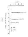
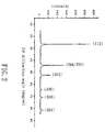
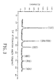
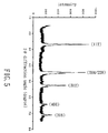
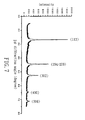
- Figs. 1 to 10 are X-ray diffraction graphs of Examples 1 to 10, respectively.
- the left peaks 112, 204/220, 312 are chalcopyrite phase peaks of the copper indium chalcogenides at different crystal faces thereof, while the right peaks 400, 316, 424 are sphalerite phase peaks of the copper indium chalcogenides at different crystal faces thereof.
- the results show that the copper indium chalcogenides powders thus formed for Examples 1-8 have a single crystal structure of a chalcopyrite phase with a trace amount of sphalerite phase.
- Figs. 9 and 10 show similar results, i.e. the copper indium chalcogenides powders thus formed for Examples 9 and 10 have a structure of a chalcopyrite phase with a trace amount of sphalerite phase.
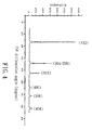
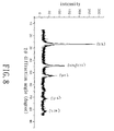
- Figs. 11 and 12 are X-ray diffraction graphs of Comparative Examples 1 and 2, respectively. The results show that no chalcopyrite phase peak of the copper indium chalcogenides for the Comparative Examples 1 and 2 was found in the graphs, which indicates that the copper indium chalcogenides was not formed in Comparative Examples 1 and 2.
- 80g of the copper indium chalcogenides powder formed from Example 6 were placed in a cavity of a mold.
- the cavity was vacuumed and the powder was heated under a heating rate of 5°C/min.
- Ar gas was introduced into the cavity.
- the powder was then heated using the same heating rate of 5°C/min to a final temperature of 780°C, and the pressure applied to the mold was raised under a rate of 1.7Mpa/min to a final pressure of 150Mpa.
- the final temperature and the final pressure for thermally pressing the copper indium chalcogenides powder were maintained for 4hr.
- the pressure applied to the mold was released, and the copper indium chalcogenides powder was cooled in the Ar environment so as to form the copper indium chalcogenides target having a diameter of 7.62cm (3inch) and a thickness of 3mm.
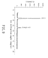
- Fig. 13 is an X-ray diffraction graph of the copper indium chalcogenides target formed in Example 11. The results show that the copper indium chalcogenides target thus formed has a single crystal structure of the chalcopyrite phase with only a trace amount of the sphalerite phase.
- a substrate was disposed in a sputtering chamber of a magnetron DC sputtering system under a working pressure of 1.06x10 -5 bar (8mtorr) that was maintained by introducing Ar gas thereinto at a flow rate of 19 sccm. Subsequently, an output power of 75W was applied on the copper indium chalcogenides target so as to form the copper indium chalcogenides thin film on the substrate.
- the substrate had a substrate temperature of 200°C and was spaced apart from the target by a distance of 10cm.
- Fig. 14 is an X-ray diffraction graph of the copper indium chalcogenides thin film formed in Example 12. The results show that the copper indium chalcogenides thin film thus formed has a single crystal structure of the chalcopyrite phase with a trace amount of the sphalerite phase.
Landscapes
- Chemical & Material Sciences (AREA)
- Organic Chemistry (AREA)
- Inorganic Chemistry (AREA)
- Powder Metallurgy (AREA)
- Manufacture And Refinement Of Metals (AREA)
- Pharmaceuticals Containing Other Organic And Inorganic Compounds (AREA)
- Photovoltaic Devices (AREA)
Claims (11)
- Verfahren zur Herstellung eines Kupfer-Indium-Chalkogenid-Pulvers, umfassend:(a) Refluxieren einer Reaktantenmischung, die ein Cu-haltiges Material, ein In-haltiges Material und ein Chalkogenid-haltiges Material enthält, in einem polaren organischen Lösungsmittel, um einen Niederschlag der Kupfer-Indium-Chalkogenide in dem polaren organischen Lösungsmittel zu bilden, wobei das polare organische Lösungsmittel ausgewählt ist aus der Gruppe bestehend aus Dimethylformamid, 1-Butyl-3-methylimidazoliumhexafluorophosphat und deren Kombinationen; und(b) Abtrennen des polaren organischen Lösungsmittels von dem Niederschlag, um das Kupfer-Indium-Chalkogenid-Pulver zu erhalten.
- Verfahren nach Anspruch 1, bei dem das Refluxieren der Reaktantenmischung in Schritt (a) unter einer Inertgasumgebung durchgeführt wird.
- Verfahren nach Anspruch 1, bei dem das Cu-haltige Material ausgewählt ist aus der Gruppe bestehend aus CuCl, CuCl2·2H2O, CuSO4 und deren Kombinationen.
- Verfahren nach Anspruch 1, bei dem das In-haltige Material ausgewählt ist aus der Gruppe bestehend aus InCl3·4H2O, In2O3, In(NO3)3 und deren Kombinationen.
- Verfahren nach Anspruch 1, bei dem das Chalkogenid-haltige Material ausgewählt ist aus der Gruppe bestehend aus Se, Na2Se, S und deren Kombinationen.
- Verfahren nach Anspruch 1, bei dem das Cu-haltige Material, das In-haltige Material und das Chalkogenid-haltige Material ein molares Konzentrationsverhältnis im Bereich von 0,9:1,1:1,9 bis 1,1:0,9:2,2 aufweisen.
- Verfahren nach Anspruch 1, bei dem die Reaktantenmischung weiter ein Gahaltiges Material enthält.
- Verfahren nach Anspruch 7, bei dem das Cu-haltige Material, das In-haltige Material, das Ga-haltige Material und das Chalkogenid-haltige Material ein molares Konzentrationsverhältnis im Bereich von 0,9:0,88:0,22:2,2 bis 1,1:0,72:0,18:1,9 aufweisen.
- Verfahren nach Anspruch 7, bei dem das Ga-haltige Material ausgewählt ist aus der Gruppe bestehend aus Ga, GaCl3 und deren Kombinationen.
- Verfahren zur Herstellung eines Kupfer-Indium-Chalkogenid-Targets, wobei das Verfahren die Herstellung eines Kupfer-Indium-Chalkogenid-Pulvers nach dem Verfahren gemäß Anspruch 1 einschließt und weiter den Schritt: (c) Anordnen des Kupfer-Indium-Chalkogenid-Pulvers in einem Hohlraum in einer Form; (d) Evakuieren des Hohlraums in der Form; (e) Erwärmen des Kupfer-Indium-Chalkogenid-Pulvers und Beaufschlagen der Form mit Druck, so dass die Form gegen das Kupfer-Indium-Chalkogenid-Pulver gepresst wird, um ein gesintertes Produkt zu bilden; und (f) Aufheben des Drucks, mit dem die Form beaufschlagt wurde, und Abkühlen der Form vor der Entfernung des gesintertes Produkts aus der Form einschließt.
- Verfahren zur Herstellung eines Kupfer-Indium-Chalkogenid-Films, wobei das Verfahren die Schritte der Herstellung eines Kupfer-Indium-Chalkogenid-Targets nach Anspruch 10 umfasst, gefolgt vom Sputtern des Kupfer-Indium-Chalkogenid-Targets.
Applications Claiming Priority (2)
| Application Number | Priority Date | Filing Date | Title |
|---|---|---|---|
| TW97103743A TW200932933A (en) | 2008-01-31 | 2008-01-31 | Method for sputtering copper indium chalcogenides thin film |
| TW97103740A TWI353344B (en) | 2008-01-31 | 2008-01-31 | Method for producing copper indium chalcogenides p |
Publications (2)
| Publication Number | Publication Date |
|---|---|
| EP2085362A1 EP2085362A1 (de) | 2009-08-05 |
| EP2085362B1 true EP2085362B1 (de) | 2011-04-20 |
Family
ID=40456866
Family Applications (1)
| Application Number | Title | Priority Date | Filing Date |
|---|---|---|---|
| EP08171213A Not-in-force EP2085362B1 (de) | 2008-01-31 | 2008-12-10 | Verfahren zur Herstellung von Kupfer-Indium-Chalcogenid-Pulver |
Country Status (4)
| Country | Link |
|---|---|
| US (1) | US20090196817A1 (de) |
| EP (1) | EP2085362B1 (de) |
| AT (1) | ATE506325T1 (de) |
| DE (1) | DE602008006346D1 (de) |
Families Citing this family (1)
| Publication number | Priority date | Publication date | Assignee | Title |
|---|---|---|---|---|
| JP2012076976A (ja) * | 2010-10-06 | 2012-04-19 | National Institute For Materials Science | 硫化物及びセレン化物粉体の合成方法 |
Family Cites Families (4)
| Publication number | Priority date | Publication date | Assignee | Title |
|---|---|---|---|---|
| US4299892A (en) * | 1975-12-17 | 1981-11-10 | Exxon Research & Engineering Co. | Amorphous and sheet dichalcogenides of Group IVb, Vb, molybdenum and tungsten |
| US5731031A (en) * | 1995-12-20 | 1998-03-24 | Midwest Research Institute | Production of films and powders for semiconductor device applications |
| JP2008540304A (ja) * | 2005-05-06 | 2008-11-20 | トランスファート プラス エスイーシー | 黄銅鉱型化合物およびその他の無機化合物の調製方法 |
| US20070099332A1 (en) * | 2005-07-07 | 2007-05-03 | Honeywell International Inc. | Chalcogenide PVD components and methods of formation |
-
2008
- 2008-10-10 US US12/249,194 patent/US20090196817A1/en not_active Abandoned
- 2008-12-10 EP EP08171213A patent/EP2085362B1/de not_active Not-in-force
- 2008-12-10 DE DE602008006346T patent/DE602008006346D1/de active Active
- 2008-12-10 AT AT08171213T patent/ATE506325T1/de not_active IP Right Cessation
Also Published As
| Publication number | Publication date |
|---|---|
| US20090196817A1 (en) | 2009-08-06 |
| EP2085362A1 (de) | 2009-08-05 |
| ATE506325T1 (de) | 2011-05-15 |
| DE602008006346D1 (de) | 2011-06-01 |
Similar Documents
| Publication | Publication Date | Title |
|---|---|---|
| Rezaee et al. | Solvent engineering as a vehicle for high quality thin films of perovskites and their device fabrication | |
| CN102912308B (zh) | 一种低相变温度二氧化钒薄膜制备工艺 | |
| TW200635113A (en) | Deposition of LiCoO2 | |
| CN111129319A (zh) | 一种CsnFA1-nPbX3钙钛矿薄膜的制备方法 | |
| KR101485522B1 (ko) | 아미노싸이올레이트를 이용한 몰리브데넘 전구체, 이의 제조방법, 및 이를 이용하여 박막을 형성하는 방법 | |
| Jia et al. | Facile synthesis of organic–inorganic hybrid perovskite CH3NH3PbI3 microcrystals | |
| US20200165171A1 (en) | Method for producing layers of silicon carbide | |
| US9142408B2 (en) | Liquid precursor for deposition of indium selenide and method of preparing the same | |
| JP5535466B2 (ja) | 金属酸化物コーティング | |
| EP2085362B1 (de) | Verfahren zur Herstellung von Kupfer-Indium-Chalcogenid-Pulver | |
| Yoon et al. | Preparation of CdS thin films through MOCVD method, using Cd-S single-source precursors | |
| Kim et al. | Preparation of copper (Cu) thin films by MOCVD and their conversion to copper selenide (CuSe) thin films through selenium vapor deposition | |
| KR101485520B1 (ko) | 아미노싸이올레이트를 이용한 텅스텐 전구체, 이의 제조방법, 및 이를 이용하여 박막을 형성하는 방법 | |
| KR100789064B1 (ko) | 금속유기물증착법에 의한 CuInS2 박막의 제조방법,그로 제조된 CuInS2 박막 및 그를 이용한 In2S3박막의 제조방법 | |
| KR101512749B1 (ko) | 황화주석 박막 형성용 전구체 및 그의 제조 방법 | |
| KR100982972B1 (ko) | ZnO 박막 제조용 전구체 및 이를 이용한화학기상증착법에 의한 ZnO 박막의 제조 방법 | |
| KR101485521B1 (ko) | 아미노싸이올레이트를 이용한 몰리브데넘 전구체, 이의 제조방법, 및 이를 이용하여 박막을 형성하는 방법 | |
| KR101540032B1 (ko) | 황화주석 박막 형성용 전구체 및 그의 제조 방법 | |
| JP5641717B2 (ja) | ドープ酸化亜鉛薄膜製造用組成物とそれを用いたドープ酸化亜鉛薄膜の製造方法 | |
| KR101757169B1 (ko) | SnS 박막 형성방법 및 이를 이용한 태양전지의 제조방법 | |
| JP2014043599A (ja) | Geクラスレートの製造方法 | |
| CN102214735A (zh) | 一种铜铟镓硒/硫太阳电池吸收层的制备方法 | |
| Zhang et al. | A Novel Ethanol-Based Non-Particulate Ink for Spin-Coating Cu2ZnSnS4 Thin Film | |
| KR101485519B1 (ko) | 아미노싸이올레이트를 이용한 텅스텐 전구체, 이의 제조방법, 및 이를 이용하여 박막을 형성하는 방법 | |
| KR101282047B1 (ko) | 수열합성법을 이용한 태양전지용 CuInSe2 입자의 제조방법 |
Legal Events
| Date | Code | Title | Description |
|---|---|---|---|
| PUAI | Public reference made under article 153(3) epc to a published international application that has entered the european phase |
Free format text: ORIGINAL CODE: 0009012 |
|
| AK | Designated contracting states |
Kind code of ref document: A1 Designated state(s): AT BE BG CH CY CZ DE DK EE ES FI FR GB GR HR HU IE IS IT LI LT LU LV MC MT NL NO PL PT RO SE SI SK TR |
|
| AX | Request for extension of the european patent |
Extension state: AL BA MK RS |
|
| 17P | Request for examination filed |
Effective date: 20100104 |
|
| AKX | Designation fees paid |
Designated state(s): AT BE BG CH CY CZ DE DK EE ES FI FR GB GR HR HU IE IS IT LI LT LU LV MC MT NL NO PL PT RO SE SI SK TR |
|
| GRAP | Despatch of communication of intention to grant a patent |
Free format text: ORIGINAL CODE: EPIDOSNIGR1 |
|
| GRAS | Grant fee paid |
Free format text: ORIGINAL CODE: EPIDOSNIGR3 |
|
| GRAA | (expected) grant |
Free format text: ORIGINAL CODE: 0009210 |
|
| AK | Designated contracting states |
Kind code of ref document: B1 Designated state(s): AT BE BG CH CY CZ DE DK EE ES FI FR GB GR HR HU IE IS IT LI LT LU LV MC MT NL NO PL PT RO SE SI SK TR |
|
| REG | Reference to a national code |
Ref country code: GB Ref legal event code: FG4D |
|
| REG | Reference to a national code |
Ref country code: CH Ref legal event code: EP |
|
| REG | Reference to a national code |
Ref country code: IE Ref legal event code: FG4D |
|
| REF | Corresponds to: |
Ref document number: 602008006346 Country of ref document: DE Date of ref document: 20110601 Kind code of ref document: P |
|
| REG | Reference to a national code |
Ref country code: DE Ref legal event code: R096 Ref document number: 602008006346 Country of ref document: DE Effective date: 20110601 |
|
| REG | Reference to a national code |
Ref country code: NL Ref legal event code: VDEP Effective date: 20110420 |
|
| LTIE | Lt: invalidation of european patent or patent extension |
Effective date: 20110420 |
|
| PG25 | Lapsed in a contracting state [announced via postgrant information from national office to epo] |
Ref country code: PT Free format text: LAPSE BECAUSE OF FAILURE TO SUBMIT A TRANSLATION OF THE DESCRIPTION OR TO PAY THE FEE WITHIN THE PRESCRIBED TIME-LIMIT Effective date: 20110822 Ref country code: NO Free format text: LAPSE BECAUSE OF FAILURE TO SUBMIT A TRANSLATION OF THE DESCRIPTION OR TO PAY THE FEE WITHIN THE PRESCRIBED TIME-LIMIT Effective date: 20110720 Ref country code: LT Free format text: LAPSE BECAUSE OF FAILURE TO SUBMIT A TRANSLATION OF THE DESCRIPTION OR TO PAY THE FEE WITHIN THE PRESCRIBED TIME-LIMIT Effective date: 20110420 Ref country code: HR Free format text: LAPSE BECAUSE OF FAILURE TO SUBMIT A TRANSLATION OF THE DESCRIPTION OR TO PAY THE FEE WITHIN THE PRESCRIBED TIME-LIMIT Effective date: 20110420 Ref country code: SE Free format text: LAPSE BECAUSE OF FAILURE TO SUBMIT A TRANSLATION OF THE DESCRIPTION OR TO PAY THE FEE WITHIN THE PRESCRIBED TIME-LIMIT Effective date: 20110420 |
|
| PG25 | Lapsed in a contracting state [announced via postgrant information from national office to epo] |
Ref country code: ES Free format text: LAPSE BECAUSE OF FAILURE TO SUBMIT A TRANSLATION OF THE DESCRIPTION OR TO PAY THE FEE WITHIN THE PRESCRIBED TIME-LIMIT Effective date: 20110731 Ref country code: GR Free format text: LAPSE BECAUSE OF FAILURE TO SUBMIT A TRANSLATION OF THE DESCRIPTION OR TO PAY THE FEE WITHIN THE PRESCRIBED TIME-LIMIT Effective date: 20110721 Ref country code: SI Free format text: LAPSE BECAUSE OF FAILURE TO SUBMIT A TRANSLATION OF THE DESCRIPTION OR TO PAY THE FEE WITHIN THE PRESCRIBED TIME-LIMIT Effective date: 20110420 Ref country code: IS Free format text: LAPSE BECAUSE OF FAILURE TO SUBMIT A TRANSLATION OF THE DESCRIPTION OR TO PAY THE FEE WITHIN THE PRESCRIBED TIME-LIMIT Effective date: 20110820 Ref country code: LV Free format text: LAPSE BECAUSE OF FAILURE TO SUBMIT A TRANSLATION OF THE DESCRIPTION OR TO PAY THE FEE WITHIN THE PRESCRIBED TIME-LIMIT Effective date: 20110420 Ref country code: AT Free format text: LAPSE BECAUSE OF FAILURE TO SUBMIT A TRANSLATION OF THE DESCRIPTION OR TO PAY THE FEE WITHIN THE PRESCRIBED TIME-LIMIT Effective date: 20110420 Ref country code: BE Free format text: LAPSE BECAUSE OF FAILURE TO SUBMIT A TRANSLATION OF THE DESCRIPTION OR TO PAY THE FEE WITHIN THE PRESCRIBED TIME-LIMIT Effective date: 20110420 Ref country code: CY Free format text: LAPSE BECAUSE OF FAILURE TO SUBMIT A TRANSLATION OF THE DESCRIPTION OR TO PAY THE FEE WITHIN THE PRESCRIBED TIME-LIMIT Effective date: 20110420 Ref country code: FI Free format text: LAPSE BECAUSE OF FAILURE TO SUBMIT A TRANSLATION OF THE DESCRIPTION OR TO PAY THE FEE WITHIN THE PRESCRIBED TIME-LIMIT Effective date: 20110420 |
|
| PG25 | Lapsed in a contracting state [announced via postgrant information from national office to epo] |
Ref country code: NL Free format text: LAPSE BECAUSE OF FAILURE TO SUBMIT A TRANSLATION OF THE DESCRIPTION OR TO PAY THE FEE WITHIN THE PRESCRIBED TIME-LIMIT Effective date: 20110420 |
|
| PG25 | Lapsed in a contracting state [announced via postgrant information from national office to epo] |
Ref country code: EE Free format text: LAPSE BECAUSE OF FAILURE TO SUBMIT A TRANSLATION OF THE DESCRIPTION OR TO PAY THE FEE WITHIN THE PRESCRIBED TIME-LIMIT Effective date: 20110420 Ref country code: CZ Free format text: LAPSE BECAUSE OF FAILURE TO SUBMIT A TRANSLATION OF THE DESCRIPTION OR TO PAY THE FEE WITHIN THE PRESCRIBED TIME-LIMIT Effective date: 20110420 |
|
| PLBE | No opposition filed within time limit |
Free format text: ORIGINAL CODE: 0009261 |
|
| STAA | Information on the status of an ep patent application or granted ep patent |
Free format text: STATUS: NO OPPOSITION FILED WITHIN TIME LIMIT |
|
| PG25 | Lapsed in a contracting state [announced via postgrant information from national office to epo] |
Ref country code: SK Free format text: LAPSE BECAUSE OF FAILURE TO SUBMIT A TRANSLATION OF THE DESCRIPTION OR TO PAY THE FEE WITHIN THE PRESCRIBED TIME-LIMIT Effective date: 20110420 Ref country code: RO Free format text: LAPSE BECAUSE OF FAILURE TO SUBMIT A TRANSLATION OF THE DESCRIPTION OR TO PAY THE FEE WITHIN THE PRESCRIBED TIME-LIMIT Effective date: 20110420 Ref country code: PL Free format text: LAPSE BECAUSE OF FAILURE TO SUBMIT A TRANSLATION OF THE DESCRIPTION OR TO PAY THE FEE WITHIN THE PRESCRIBED TIME-LIMIT Effective date: 20110420 Ref country code: DK Free format text: LAPSE BECAUSE OF FAILURE TO SUBMIT A TRANSLATION OF THE DESCRIPTION OR TO PAY THE FEE WITHIN THE PRESCRIBED TIME-LIMIT Effective date: 20110420 |
|
| 26N | No opposition filed |
Effective date: 20120123 |
|
| REG | Reference to a national code |
Ref country code: DE Ref legal event code: R097 Ref document number: 602008006346 Country of ref document: DE Effective date: 20120123 |
|
| PG25 | Lapsed in a contracting state [announced via postgrant information from national office to epo] |
Ref country code: IT Free format text: LAPSE BECAUSE OF FAILURE TO SUBMIT A TRANSLATION OF THE DESCRIPTION OR TO PAY THE FEE WITHIN THE PRESCRIBED TIME-LIMIT Effective date: 20110420 |
|
| PG25 | Lapsed in a contracting state [announced via postgrant information from national office to epo] |
Ref country code: MC Free format text: LAPSE BECAUSE OF NON-PAYMENT OF DUE FEES Effective date: 20111231 |
|
| REG | Reference to a national code |
Ref country code: FR Ref legal event code: ST Effective date: 20120831 |
|
| REG | Reference to a national code |
Ref country code: IE Ref legal event code: MM4A |
|
| PG25 | Lapsed in a contracting state [announced via postgrant information from national office to epo] |
Ref country code: IE Free format text: LAPSE BECAUSE OF NON-PAYMENT OF DUE FEES Effective date: 20111210 |
|
| PG25 | Lapsed in a contracting state [announced via postgrant information from national office to epo] |
Ref country code: MT Free format text: LAPSE BECAUSE OF FAILURE TO SUBMIT A TRANSLATION OF THE DESCRIPTION OR TO PAY THE FEE WITHIN THE PRESCRIBED TIME-LIMIT Effective date: 20110420 |
|
| PGFP | Annual fee paid to national office [announced via postgrant information from national office to epo] |
Ref country code: GB Payment date: 20121212 Year of fee payment: 5 |
|
| PG25 | Lapsed in a contracting state [announced via postgrant information from national office to epo] |
Ref country code: FR Free format text: LAPSE BECAUSE OF NON-PAYMENT OF DUE FEES Effective date: 20120102 |
|
| PGFP | Annual fee paid to national office [announced via postgrant information from national office to epo] |
Ref country code: DE Payment date: 20121227 Year of fee payment: 5 |
|
| PG25 | Lapsed in a contracting state [announced via postgrant information from national office to epo] |
Ref country code: LU Free format text: LAPSE BECAUSE OF NON-PAYMENT OF DUE FEES Effective date: 20111210 |
|
| PG25 | Lapsed in a contracting state [announced via postgrant information from national office to epo] |
Ref country code: BG Free format text: LAPSE BECAUSE OF FAILURE TO SUBMIT A TRANSLATION OF THE DESCRIPTION OR TO PAY THE FEE WITHIN THE PRESCRIBED TIME-LIMIT Effective date: 20110720 |
|
| REG | Reference to a national code |
Ref country code: CH Ref legal event code: PL |
|
| PG25 | Lapsed in a contracting state [announced via postgrant information from national office to epo] |
Ref country code: TR Free format text: LAPSE BECAUSE OF FAILURE TO SUBMIT A TRANSLATION OF THE DESCRIPTION OR TO PAY THE FEE WITHIN THE PRESCRIBED TIME-LIMIT Effective date: 20110420 |
|
| PG25 | Lapsed in a contracting state [announced via postgrant information from national office to epo] |
Ref country code: LI Free format text: LAPSE BECAUSE OF NON-PAYMENT OF DUE FEES Effective date: 20121231 Ref country code: HU Free format text: LAPSE BECAUSE OF FAILURE TO SUBMIT A TRANSLATION OF THE DESCRIPTION OR TO PAY THE FEE WITHIN THE PRESCRIBED TIME-LIMIT Effective date: 20110420 Ref country code: CH Free format text: LAPSE BECAUSE OF NON-PAYMENT OF DUE FEES Effective date: 20121231 |
|
| REG | Reference to a national code |
Ref country code: DE Ref legal event code: R119 Ref document number: 602008006346 Country of ref document: DE |
|
| GBPC | Gb: european patent ceased through non-payment of renewal fee |
Effective date: 20131210 |
|
| REG | Reference to a national code |
Ref country code: DE Ref legal event code: R119 Ref document number: 602008006346 Country of ref document: DE Effective date: 20140701 |
|
| PG25 | Lapsed in a contracting state [announced via postgrant information from national office to epo] |
Ref country code: DE Free format text: LAPSE BECAUSE OF NON-PAYMENT OF DUE FEES Effective date: 20140701 |
|
| PG25 | Lapsed in a contracting state [announced via postgrant information from national office to epo] |
Ref country code: GB Free format text: LAPSE BECAUSE OF NON-PAYMENT OF DUE FEES Effective date: 20131210 |