EP2081241A1 - Durchführung für eine Batterie, Verfahren zur Herstellung derselben und Batterie - Google Patents
Durchführung für eine Batterie, Verfahren zur Herstellung derselben und Batterie Download PDFInfo
- Publication number
- EP2081241A1 EP2081241A1 EP08170923A EP08170923A EP2081241A1 EP 2081241 A1 EP2081241 A1 EP 2081241A1 EP 08170923 A EP08170923 A EP 08170923A EP 08170923 A EP08170923 A EP 08170923A EP 2081241 A1 EP2081241 A1 EP 2081241A1
- Authority
- EP
- European Patent Office
- Prior art keywords
- coating
- connection element
- battery
- pin
- flange
- Prior art date
- Legal status (The legal status is an assumption and is not a legal conclusion. Google has not performed a legal analysis and makes no representation as to the accuracy of the status listed.)
- Granted
Links
Images
Classifications
-
- H—ELECTRICITY
- H01—ELECTRIC ELEMENTS
- H01M—PROCESSES OR MEANS, e.g. BATTERIES, FOR THE DIRECT CONVERSION OF CHEMICAL ENERGY INTO ELECTRICAL ENERGY
- H01M50/00—Constructional details or processes of manufacture of the non-active parts of electrochemical cells other than fuel cells, e.g. hybrid cells
- H01M50/10—Primary casings; Jackets or wrappings
- H01M50/183—Sealing members
- H01M50/186—Sealing members characterised by the disposition of the sealing members
-
- H—ELECTRICITY
- H01—ELECTRIC ELEMENTS
- H01M—PROCESSES OR MEANS, e.g. BATTERIES, FOR THE DIRECT CONVERSION OF CHEMICAL ENERGY INTO ELECTRICAL ENERGY
- H01M50/00—Constructional details or processes of manufacture of the non-active parts of electrochemical cells other than fuel cells, e.g. hybrid cells
- H01M50/10—Primary casings; Jackets or wrappings
- H01M50/172—Arrangements of electric connectors penetrating the casing
-
- H—ELECTRICITY
- H01—ELECTRIC ELEMENTS
- H01M—PROCESSES OR MEANS, e.g. BATTERIES, FOR THE DIRECT CONVERSION OF CHEMICAL ENERGY INTO ELECTRICAL ENERGY
- H01M50/00—Constructional details or processes of manufacture of the non-active parts of electrochemical cells other than fuel cells, e.g. hybrid cells
- H01M50/10—Primary casings; Jackets or wrappings
- H01M50/183—Sealing members
- H01M50/19—Sealing members characterised by the material
- H01M50/191—Inorganic material
-
- H—ELECTRICITY
- H01—ELECTRIC ELEMENTS
- H01M—PROCESSES OR MEANS, e.g. BATTERIES, FOR THE DIRECT CONVERSION OF CHEMICAL ENERGY INTO ELECTRICAL ENERGY
- H01M50/00—Constructional details or processes of manufacture of the non-active parts of electrochemical cells other than fuel cells, e.g. hybrid cells
- H01M50/50—Current conducting connections for cells or batteries
- H01M50/543—Terminals
- H01M50/552—Terminals characterised by their shape
-
- H—ELECTRICITY
- H01—ELECTRIC ELEMENTS
- H01M—PROCESSES OR MEANS, e.g. BATTERIES, FOR THE DIRECT CONVERSION OF CHEMICAL ENERGY INTO ELECTRICAL ENERGY
- H01M50/00—Constructional details or processes of manufacture of the non-active parts of electrochemical cells other than fuel cells, e.g. hybrid cells
- H01M50/50—Current conducting connections for cells or batteries
- H01M50/571—Methods or arrangements for affording protection against corrosion; Selection of materials therefor
-
- H—ELECTRICITY
- H01—ELECTRIC ELEMENTS
- H01M—PROCESSES OR MEANS, e.g. BATTERIES, FOR THE DIRECT CONVERSION OF CHEMICAL ENERGY INTO ELECTRICAL ENERGY
- H01M50/00—Constructional details or processes of manufacture of the non-active parts of electrochemical cells other than fuel cells, e.g. hybrid cells
- H01M50/50—Current conducting connections for cells or batteries
- H01M50/572—Means for preventing undesired use or discharge
-
- Y—GENERAL TAGGING OF NEW TECHNOLOGICAL DEVELOPMENTS; GENERAL TAGGING OF CROSS-SECTIONAL TECHNOLOGIES SPANNING OVER SEVERAL SECTIONS OF THE IPC; TECHNICAL SUBJECTS COVERED BY FORMER USPC CROSS-REFERENCE ART COLLECTIONS [XRACs] AND DIGESTS
- Y02—TECHNOLOGIES OR APPLICATIONS FOR MITIGATION OR ADAPTATION AGAINST CLIMATE CHANGE
- Y02E—REDUCTION OF GREENHOUSE GAS [GHG] EMISSIONS, RELATED TO ENERGY GENERATION, TRANSMISSION OR DISTRIBUTION
- Y02E60/00—Enabling technologies; Technologies with a potential or indirect contribution to GHG emissions mitigation
- Y02E60/10—Energy storage using batteries
Definitions
- the present invention relates to a passage for a battery having a first connection element and a second connection element, which are at different electrical potential. Furthermore, the present invention relates to a method for producing such a passage and a battery having at least one such implementation.
- a feedthrough In hermetically sealed batteries, as z.
- glass-metal feedthroughs or ceramic feedthroughs are used, which ensure a gas-tight, electrically insulated passage of a battery pole through the metallic housing.
- Such a feedthrough has a first connection element in the form of a pin and a second connection element in the form of a flange element, which are at different electrical potential (positive pole, negative pole). Due to the small distance between the metallic pin and the metallic flange element, even small amounts of electrically conductive material in the interior of the bushing are sufficient to produce a short circuit of the battery.
- Such conductive materials which generate a short circuit can arise due to the fact that the electrode materials within the battery dissolve in the electrolyte on account of the available potential differences.
- lithium batteries under certain conditions, for example, lithium in the form of lithium cations may go into solution. These lithium cations can deposit on battery components with anodic potential in the form of elemental lithium.
- critical components within the battery are isolated. For example, an electrically insulating layer prevents the transfer of electrons to the ions of the electrolyte. Deposition is thus prevented.
- a metal deposit prevented by the suppression of the wetting of the electrolyte of electrically conductive components.
- the object of the present invention is therefore to provide a bushing, which avoids an electrical short circuit between pin and flange effectively, especially over a long life of the battery. It is also the task of creating a corresponding battery.
- the object is additionally to provide a method for producing such a procedure, which is simple and inexpensive.
- the above object is achieved by an implementation which on the first connection element and / or the second connection element has a short circuit between the first connection element and the second connection element preventing coating which is produced by means of chemical vapor deposition (CVD).
- CVD chemical vapor deposition
- chemical vapor deposition means a process in which a solid component is deposited on the heated surface of a substrate due to a chemical reaction from the gas phase.
- volatile compounds of the layer components exist that deposit the solid layer at a certain reaction temperature.
- the process of chemical vapor deposition is characterized by at least one reaction on the surface of the workpiece to be coated. At least two gaseous starting compounds (starting materials) and at least two reaction products - at least one of which is gaseous and at least one in the solid phase - must be involved in this reaction.
- the chemical vapor deposition allows a non-porous coating of complex, three-dimensionally shaped surfaces.
- a compliant i. homogeneous CVD layer deposition applied, which produces a closed layer.
- a coating thus prepared contains the compound parylene, preferably the coating consists entirely of parylene.
- a coating has very good adhesive properties. This is especially true for typical materials used in a feedthrough (as a first mating material, for example, stainless steel or molybdenum, and as a second mating material, for example, stainless steel or titanium).
- Parylene is chemically inert to the components of typical battery electrolytes, so that the coating neither dissolves nor swells. This ensures that no components of the coating get into the electrolyte.
- the parylene coating also has a high temperature resistance.
- the parylene preferably used in the chemical vapor deposition is also characterized in that Parylene forms a hydrophobic, chemically resistant coating with excellent barrier to inorganic and organic media, strong acids, alkalis, gases and water vapor.
- Parylene produces a superior electrical insulation layer with high withstand voltage and low dielectric constant.
- the coating is biostable and biocompatible and FDA approved. From a layer thickness of about 0.2 .mu.m, the parylene layer can be produced by means of chemical vapor deposition microporous and pinhohl arthritis. CVD makes it possible to produce a thin and transparent parylene coating with a high degree of splitting, which is suitable for complex substrates or edges.
- the coating can be prepared without exposure to temperature of the substrates, it takes place at room temperature in a vacuum.
- the Parylene coating also forms a corrosion protection.
- CVD also makes it possible to form an absolutely uniform layer.
- the coating is temperature resistant up to 200 ° C and mechanically stable in the range of about -200 ° C to about + 150 ° C.
- the Parylene coating causes low mechanical stresses, is abrasion resistant, does not degrade and has a high dielectric strength.
- the thickness of the coating is about 1 ⁇ m to about 100 ⁇ m, more preferably between about 3 ⁇ m to about 40 ⁇ m. This thickness has the advantage that a closed pore-free layer is formed, but cracking by stresses within the coating does not yet occur.
- the coating completely covers the respective section of the lateral surface of the pin as well as the respective end faces of glass seal and flange element, so that there is a coherent coating surface which extends over these three elements of the bushing.
- the coated area of the lateral surface of the pin is connected directly to the glass melt on the battery side.
- This preferred arrangement of the coating is a simple way of a particularly effective sealing of the first connection element and second connection element against the electrolyte and an electrical insulation of the first connection element and second connection element achieved.
- At least partially a silicone encapsulation is arranged on the surface of the coating. This casting takes on an additional sealing function.
- a battery having at least one above-mentioned, inventive implementation.
- Such a battery has the advantage that it is very durable and short circuits of the current-carrying components are effectively prevented.
- the above object is further achieved by a method for producing a bushing in which first the bushing with the first connection element and a second connection element mechanically connected to the first connection element is provided and then a coating which prevents a short circuit between the second connection element and the first connection element and preferably contains parylene , is applied by chemical vapor deposition (CVD) on the first and / or second connection element.
- CVD chemical vapor deposition
- PECVD plasma-enhanced chemical vapor deposition
- the generation of the plasma takes place in the context of the present invention preferably capacitively by electromagnetic fields or by microwave radiation.
- a sufficiently strong alternating electric field is usually applied to two plates, between which the plasma is formed.
- charged particles oscillate back and forth with the frequency of the alternating field.
- the field strength of the electromagnetic wave must first be high enough to cause electrical breakdown and impact ionization.
- the magnetron adapts to the then changed field strength and impedance conditions.
- Other ways to generate the plasma consist in the thermal excitation by means of chemical reactions, the radiation excitation by means of laser radiation, the excitation by DC voltage and the excitation by electromagnetic fields by means of an inductively (magnetically) operating device.
- the chemical vapor deposition takes place at a pressure of about 0.5 hPa to about 0.01 hPa, preferably at about 0.1 hPa.
- a plasma post-treatment of the applied layer can be carried out, which leads to the activation of the surface of the coating.
- This activated surface forms the basis for additional security measures of the implementation.
- such a coated implementation can then be potted with silicone resin. In this way, several protective measures can be applied in parallel, so that the safety of the batteries, especially in sensitive applications such as in medical technology, is further increased.
- the components in particular the first connection element and / or the second connection element, are subjected to a plasma ultra-fine cleaning prior to coating.
- a plasma ultra-fine cleaning prior to coating.
- all organic impurities on the surface of the passage are removed by oxidation in a plasma in the presence of oxygen.
- highly cleaned surfaces cause optimal adhesion of the coating on the substrate.
- Such cleaning stabilizes the reproducibility of the coating process.
- the coating is cast by means of a silicone resin.
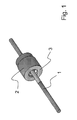
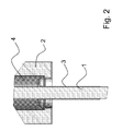
- the in the FIGS. 1 and 2 illustrated glass-metal feedthrough has a cylindrical pin 1 as a first connection element and a pin-1 surrounding, hollow cylindrical flange 2 as a second connection element.
- the pin 1 is arranged concentrically in the central opening of the flange element 2, wherein a glass seal 4 is provided between pin 1 and flange element 2.
- the glass seal 4 is arranged in the opening of the flange element 2 in such a way that it is slightly set back from the battery-side end face of the flange element 2.
- the battery-side end surface of the flange 2 and the battery-side end face of the glass seal 4 and a portion of the lateral surface of the pin 1, the battery side protruding from the glass seal 4 are provided with a CVD coating 3, which consists of Parylene.
- the pin 1 represents in the implementation of the positive pole and the flange 2 is the negative terminal.
- the parylene coating is produced by chemical vapor deposition.
- Starting material is di-para-xylylene or their halogenated substituents which form stable compounds at room temperature.
- the starting material is evaporated and passed through a high temperature zone. This forms a highly reactive Monomer, a so-called para-xylylene diradical, which immediately reacts on the surface to be coated to form a chain-like polymer.
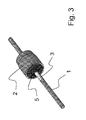
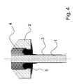
- FIG. 3 and 4 is another embodiment of the present invention is shown in which a part of the battery-side end face of the flange 2 and the battery-side end face of the glass seal 4 and a portion of the lateral surface of the pin 1, the battery side protruding from the glass seal 4, with a silicone -Verguss 5 are provided.
- the potting 5 is applied to the coating 3 and extends only over part of the surface of pin 1, flange 2 and glass seal 4, which are provided with the parylene coating 3.
- the silicone potting 5 consists of a silicone resin.
Landscapes
- Chemical & Material Sciences (AREA)
- Chemical Kinetics & Catalysis (AREA)
- Electrochemistry (AREA)
- General Chemical & Material Sciences (AREA)
- Inorganic Chemistry (AREA)
- Sealing Battery Cases Or Jackets (AREA)
- Secondary Cells (AREA)
- Primary Cells (AREA)
Abstract
Description
- Die vorliegende Erfindung betrifft eine Durchführung für eine Batterie mit einem ersten Anschlusselement und einem zweiten Anschlusselement, welche auf unterschiedlichem elektrischen Potential liegen. Ferner betrifft die vorliegende Erfindung ein Verfahren zur Herstellung einer derartigen Durchführung sowie eine Batterie mit mindestens einer derartigen Durchführung.
- In hermetisch verschlossenen Batterien, wie sie z. B. in medizinischen Implantaten verwendet werden, kommen Glas-Metall-Durchführungen oder keramische Durchführungen zum Einsatz, die eine gasdichte, elektrisch isolierte Durchführung eines Batterie-Pols durch das metallische Gehäuse sicherstellen. Eine derartige Durchführung weist ein erstes Anschlusselement in Form eines Pins und ein zweites Anschlusselement in Form eines Flanschelements auf, welche auf unterschiedlichem elektrischem Potential (Pluspol, Minuspol) liegen. Aufgrund des geringen Abstands zwischen dem metallischen Pin und dem metallischen Flanschelement reichen bereits geringe Mengen an elektrisch leitfähigem Material im Innenbereich der Durchführung aus, um einen Kurzschluss der Batterie zu erzeugen.
- Derartige, einen Kurzschluss erzeugende leitfähige Materialien, können dadurch entstehen, dass sich die Elektrodenmaterialien innerhalb der Batterie aufgrund der vorliegenden Potentialdifferenzen im Elektrolyten auflösen. Im Fall von Lithium-Batterien kann unter bestimmten Bedingungen beispielsweise Lithium in Form von Lithium-Kationen in Lösung gehen. Diese Lithium-Kationen können sich auf Batteriebauteilen mit anodischem Potential in Form von elementarem Lithium abscheiden. Bei bekannten Batterien werden, um zu vermeiden, dass durch eine derartige Abscheidung Kurzschlüsse innerhalb der Batterien hervorgerufen werden, kritische Bauteile innerhalb der Batterie isoliert. Z.B. verhindert eine elektrisch isolierende Schicht die Übertragung von Elektronen auf die Ionen des Elektrolyten. Eine Abscheidung wird somit verhindert. Ferner wird eine Metallabscheidung durch die Unterbindung der Benetzung des Elektrolyten von elektrisch leitfähigen Bauteilen verhindert.
- Bei herkömmlichen Batterien werden Glas-Metall-Durchführungen oder keramische Durchführungen, um die oben angegebenen Probleme zu vermeiden, an der Innenseite der Batterie verschlossen. Der Verschluss erfolgt in der Regel durch Vergießen mit einem Polymerharz oder durch einen Polymer-Stopfen, der auf den Pin der Durchführung aufgeschoben wird. Diese Vorgehensweise lässt sich allerdings bei sehr kleinen Durchführungen nur schwierig realisieren. Außerdem sind bei geringem Abstand zwischen Flanschelement und Pin lediglich Vergussmaterialien mit sehr geringer Viskosität geeignet, so dass die Auswahl an Vergussmaterialien begrenzt ist. Die Auswahl wird zusätzlich dadurch begrenzt, da diese Materialien keine elektrolytlöslichen Bestandteile enthalten dürfen, um zu verhindern, dass der Elektrolyt das Vergussmaterial beschädigt. Die technische Realisierung des Vergießens ist außerdem dadurch erschwert, dass der Verguss poren- und lunkerfrei erfolgen muss. Bei der Verwendung von Polymer-Stopfen besteht das Problem, dass diese sich meist nur schwer vollständig gegenüber Pin und Flanschelement abdichten lassen.
- Die Aufgabe der vorliegenden Erfindung besteht somit darin, eine Durchführung zu schaffen, welche einen elektrischen Kurzschluss zwischen Pin und Flanschelement effektiv, vor allem über eine lange Lebensdauer der Batterie, vermeidet. Es ist außerdem die Aufgabe, eine entsprechende Batterie zu schaffen. Die Aufgabe besteht zusätzlich darin, ein Verfahren zur Herstellung einer derartigen Durchführung anzugeben, das einfach und kostengünstig ist.
- Die oben angegebene Aufgabe wird durch eine Durchführung gelöst, welche auf dem ersten Anschlusselement und/oder dem zweiten Anschlusselement einen Kurzschluss zwischen dem erstem Anschlusselement und dem zweitem Anschlusselement verhindernde Beschichtung aufweist, die mittels chemischer Gasphasenabscheidung (CVD) hergestellt ist.
- Unter dem Begriff "chemische Gasphasenabscheidung" (Englisch: chemical vapor deposition, CVD) wird ein Verfahren verstanden, bei dem an der erhitzten Oberfläche eines Substrats aufgrund einer chemischen Reaktion aus der Gasphase eine Feststoffkomponente abgeschieden wird. Hierfür müssen flüchtige Verbindungen der Schichtkomponenten existieren, die bei einer bestimmten Reaktionstemperatur die feste Schicht abscheiden. Das Verfahren der chemischen Gasphasenabscheidung zeichnet sich durch mindestens eine Reaktion an der Oberfläche des zu beschichtenden Werkstücks aus. An dieser Reaktion müssen mindestens zwei gasförmige Ausgangsverbindungen (Edukte) und mindestens zwei Reaktionsprodukte - davon mindestens eines gasförmig und mindestens eines in der festen Phase - beteiligt sein. Die chemische Gasphasenabscheidung ermöglicht eine porenfreie Beschichtung von komplexen, dreidimensional geformten Oberflächen. Hierdurch können beispielsweise feinste Vertiefungen oder auch Hohlkörper auf ihrer Innenseite gleichmäßig beschichtet werden, so dass ein Kurzschluss zwischen erstem Anschlusselement und zweitem Anschlusselement effektiv verhindert wird. Aufgrund der Porenfreiheit der Beschichtung wirkt diese sowohl als elektrische als auch als mechanische Grenzschicht zwischen den metallischen Bauteilen und dem Elektrolyten. Da die Beschichtung bei Raumtemperatur im Vakuum stattfindet, wird die Durchführung beim Beschichten keiner Temperaturbelastung ausgesetzt, so dass die Einglasung oder die Keramik nicht beschädigt wird. Ein weiterer Vorteil der Aufbringung einer isolierenden Beschichtung mittels CVD besteht darin, dass Teile der Bauteile der Durchführung, die nicht beschichtet werden sollen, abdeckt werden können. Vorliegend trifft dies beispielsweise auf die Mantelfläche des zweiten Anschlusselements in Form eines Flanschelements zu, da der Flansch bei der Verwendung der Durchführung in einer Batterie an der Mantelfläche verschweißt wird und deshalb keine Beschichtung aufweisen darf.
- Besonders bevorzugt wird eine konforme, d.h. homogene CVD-Schichtabscheidung angewendet, welche eine geschlossene Schicht erzeugt.
- In einem Ausführungsbeispiel enthält eine so hergestellte Beschichtung die Verbindung Parylene, vorzugsweise besteht die Beschichtung vollständig aus Parylene. Eine derartige Beschichtung weist sehr gute Hafteigenschaften auf. Dies trifft insbesondere auf typische Materialien, die in einer Durchführung verwendet werden (als erstes Anschlusselement-Material beispielsweise Edelstahl oder Molybdän und als zweites Anschlusselement-Material beispielsweise Edelstahl oder Titan), zu. Ferner ist Parylene chemisch inert gegenüber den Bestandteilen typischer Batterie-Elektrolyte, so dass sich die Beschichtung weder auflöst noch aufquillt. Dadurch wird sichergestellt, dass keine Bestandteile der Beschichtung in die Elektrolyten gelangen. Die Parylene-Beschichtung weist zudem eine hohe Temperaturbeständigkeit auf.
- Das bei der chemischen Gasphasenabscheidung vorzugsweise verwendete Parylene zeichnet sich außerdem dadurch aus, dass Parylene eine hydrophobe, chemisch resistente Beschichtung mit einer hervorragenden Barrierewirkung gegenüber anorganischen und organischen Medien, starken Säuren, Laugen, Gasen und Wasserdampf bildet. Außerdem erzeugt Parylene eine hervorragende elektrische Isolationsschicht mit einer hohen Spannungsfestigkeit und einer niedrigen Dielektrizitätskonstante. Zudem ist die Beschichtung biostabil und biokompatibel und bei der FDA zugelassen. Ab einer Schichtdicke von etwa 0,2 µm kann die Paryleneschicht mittels der chemischen Gasphasenabscheidung mikroporen- und pinhohlfrei hergestellt werden. Mittels CVD lässt sich eine dünne und transparente Parylene-Beschichtung mit hoher Spaltgängigkeit herstellen, die für komplex gestaltete Substrate oder Kanten geeignet ist. Mittels CVD kann die Beschichtung ohne Temperaturbelastung der Substrate hergestellt werden, sie erfolgt bei Raumtemperatur im Vakuum. Die Parylene-Beschichtung bildet zudem einen Korrosionsschutz. Mittels CVD lässt sich außerdem eine absolut gleichförmige Schicht ausbilden. Die Beschichtung ist temperaturbeständig bis zu 200°C und mechanisch stabil im Bereich von etwa -200°C bis etwa +150°C. Die Parylene-Beschichtung verursacht niedrige mechanische Spannungen, ist abriebfest, gast nicht aus und weist eine hohe elektrische Durchschlagfestigkeit auf.
- In einer bevorzugten Ausführung beträgt die Dicke der Beschichtung etwa 1 µm bis etwa 100 µm, besonders bevorzugt zwischen etwa 3 µm bis etwa 40 µm. Diese Dicke hat den Vorteil, dass eine geschlossene porenfreie Schicht ausgebildet wird, aber noch keine Rissbildung durch Spannungen innerhalb der Beschichtung auftreten.
- In einem unten dargestellten Ausführungsbeispiel ist die Beschichtung auf einem Bereich der Mantelfläche des ersten Anschlusselements in Form eines Pins, der aus dem zweiten Anschlusselement in Form eines Flanschelements batterieseitig herausragt, der batterieseitigen Stirnfläche des zweiten Anschlusselements sowie der batterieseitigen Stirnfläche der zwischen erstem Anschlusselement und zweitem Anschlusselement angeordneten Glas-Einschmelzung angeordnet. Die Beschichtung bedeckt dabei den jeweiligen Abschnitt der Mantelfläche des Pins sowie die jeweiligen die Stirnflächen von Glas-Einschmelzung und Flanschelement vollständig, so dass eine zusammenhängende Beschichtungsfläche vorliegt, die sich über diese drei Elemente der Durchführung erstreckt. Der beschichtete Bereich der Mantelfläche des Pins schließt sich batterieseitig direkt an die Glaseinschmelzung an. Durch diese bevorzugte Anordnung der Beschichtung wird auf einfache Weise eine besonders effektive Abdichtung von erstem Anschlusselement und zweitem Anschlusselement gegen den Elektrolyten sowie eine elektrische Isolierung von erstem Anschlusselement und zweitem Anschlusselement erzielt.
- In einem weiteren Ausführungsbeispiel ist auf der Oberfläche der Beschichtung mindestens teilweise einen Silikon-Verguss angeordnet. Dieser Verguss übernimmt eine zusätzliche Abdichtungsfunktion.
- Die obige Aufgabe wird außerdem gelöst durch eine Batterie mit mindestens einer oben angegebenen, erfindungsgemäßen Durchführung. Eine derartige Batterie hat den Vorteil, dass sie sehr langlebig ist und Kurzschlüsse der stromführenden Komponenten effektiv verhindert werden.
- Die obige Aufgabenstellung wird ferner gelöst durch ein Verfahren zur Herstellung einer Durchführung bei dem zunächst die Durchführung mit erstem Anschlusselement und einem mit dem erstem Anschlusselement mechanisch verbundenen zweiten Anschlusselement bereitgestellt und anschließend eine einen Kurzschluss zwischen zweitem Anschlusselement und erstem Anschlusselement verhindernde Beschichtung, welche vorzugsweise Parylene enthält, mittels chemischer Gasphasenabscheidung (CVD) auf dem ersten und/oder zweiten Anschlusselement aufgebracht wird. Die Aufbringung der Beschichtung mittels CVD hat die oben erläuterten Vorteile.
- Weiterhin bevorzugt ist die Anwendung einer Plasma-unterstützten chemischen Gasphasenabscheidung (Englisch: plasma enhanced chemical vapor deposition, PECVD). Durch die PECVD kann die Temperaturbelastung des Substrats reduziert werden, da oberhalb des Substrats ein Hochfrequenz-Plasma gezündet wird, durch das die eingeleiteten Gase angeregt werden. Hierdurch ist eine Reduzierung der Reaktionsenergie und somit eine niedrigere Prozesstemperatur möglich. Eine Beschichtung kann daher bei Raumtemperatur erfolgen.
- Die Erzeugung des Plasmas erfolgt im Zusammenhang mit der vorliegenden Erfindung vorzugsweise kapazitiv durch elektromagnetische Felder oder durch Mikrowellenstrahlung. Zur Herstellung eines kapazitiv erzeugten Plasmas wird in der Regel ein ausreichend starkes elektrisches Wechselfeld an zwei Platten angelegt, zwischen denen sich das Plasma ausbildet. In dem Plasma oszillieren geladene Teilchen mit der Frequenz des Wechselfeldes hin und her. Bei einer Anregung des Plasmas durch Mikrowellenstrahlung wird diese durch ein Magnetron in den Reaktionsraum geleitet. Zum Zünden des Plasmas muss die Feldstärke der elektromagnetischen Welle zunächst hoch genug sein, um einen elektrischen Durchbruch und Stoßionisation hervorzurufen. Nach der Zündung des Plasmas passt sich der Magnetron an die dann geänderten Feldstärken- und Impedanzverhältnisse an. Weitere Möglichkeiten, das Plasma zu erzeugen, bestehen in der thermischen Anregung mittels chemischer Reaktionen, der Strahlungsanregung mittels Laserstrahlung, der Anregung durch Gleichspannung und der Anregung durch elektromagnetische Felder mittels einer induktiv (magnetisch) arbeitenden Vorrichtung.
- Besonders bevorzugt erfolgt die chemische Gasphasenabscheidung bei einem Druck von etwa 0,5 hPa bis etwa 0,01 hPa, vorzugsweise bei etwa 0,1 hPa.
- In einem besonders bevorzugten Ausführungsbeispiel kann nach der CVD- oder PECVD-Beschichtung eine Plasma-Nachbehandlung der aufgebrachten Schicht durchgeführt werden, welche zur Aktivierung der Oberfläche der Beschichtung führt. Diese aktivierte Oberfläche stellt die Grundlage für zusätzliche Sicherungsmaßnahmen der Durchführung dar. Beispielsweise kann eine derartig beschichtete Durchführung anschließend mit Silikonharz vergossen werden. Auf diese Weise können mehrere Schutzmaßnahmen parallel angewendet werden, so dass die Sicherheit der Batterien, insbesondere bei sensiblen Anwendungen wie in der Medizintechnik, zusätzlich erhöht wird.
- In einem weiteren bevorzugten Ausführungsbeispiel werden die Bauteile, insbesondere das erste Anschlusselement und/oder das zweite Anschlusselement vor der Beschichtung einer Plasma-Ultra-Feinreinigung unterzogen. Hierbei werden in einem Plasma unter Anwesenheit von Sauerstoff alle organischen Verunreinigungen auf der Oberfläche der Durchführung oxidativ entfernt. Auf diese Weise hochgereinigte Oberflächen bewirken eine optimale Haftung der Beschichtung auf dem Substrat. Eine derartige Reinigung stabilisiert die Reproduzierbarkeit des Beschichtungsprozesses.
- In einem weiteren Ausführungsbeispiel wird nach der Plasma-Nachbehandlung oder nach dem Beschichtungsprozess die Beschichtung mittels eines Silikonharzes vergossen.
- Weitere Ziele, Merkmale, Vorteile und Anwendungsmöglichkeiten der Erfindung ergeben sich aus der nachfolgenden Beschreibung eines Ausführungsbeispiels anhand der Figuren. Dabei bilden alle beschriebenen und/oder bildlich dargestellten Merkmale für sich oder in beliebiger Kombination den Gegenstand der vorliegenden Erfindung, auch unabhängig von ihrer Zusammenfassung in den einzelnen Ansprüchen oder deren Rückbeziehung.
- Es zeigen schematisch:
- Fig. 1
- eine perspektivische Ansicht eines ersten Ausführungsbeispiels einer erfindungsgemäßen Durchführung von der Seite und
- Fig. 2
- das batterieseitige Ende eines Querschnitts der erfindungsgemäßen Durchführung gemäß
Fig. 1 , - Fig. 3
- eine perspektivische Ansicht eines zweiten Ausführungsbeispiels einer erfindungsgemäßen Durchführung von der Seite und
- Fig. 4
- das batterieseitige Ende eines Querschnitts der erfindungsgemäßen Durchführung gemäß
Fig. 3 . - Die in den
Figuren 1 und2 dargestellte Glas-Metall-Durchführung weist einen zylinderförmigen Pin 1 als erstes Anschlusselement und ein den Pin 1 umgebendes, hohlzylinderförmiges Flanschelement 2 als zweitens Anschlusselement auf. Der Pin 1 ist konzentrisch in der mittigen Öffnung des Flanschelements 2 angeordnet, wobei zwischen Pin 1 und Flanschelement 2 eine Glas-Einschmelzung 4 vorgesehen ist. Die Glas-Einschmelzung 4 ist derart in der Öffnung des Flanschelements 2 angeordnet, dass sie von der batterieseitigen Stirnfläche des Flanschelements 2 etwas zurückversetzt ist. Die batterieseitige Stirnfläche des Flanschelements 2 und die batterieseitige Stirnfläche der Glas-Einschmelzung 4 sowie ein Bereich der Mantelfläche des Pins 1, der aus der Glas-Einschmelzung 4 batterieseitig hervorsteht, sind mit einer CVD-Beschichtung 3 versehen, die aus Parylene besteht. Der Pin 1 stellt bei der Durchführung den Pluspol und das Flanschelement 2 den Minuspol dar. - Die Parylene-Beschichtung wird mittels einer chemischen Gasphasenabscheidung erzeugt. Ausgangsmaterial ist Di-Para-Xylylen oder deren halogenierte Substituenten, die bei Raumtemperatur stabile Verbindungen ausbilden. Das Ausgangsmaterial wird verdampft und durch eine Hochtemperaturzone geleitet. Hierbei bildet sich ein hochreaktives Monomer, ein sogenanntes Para-Xylylen-Diradikal, das auf der zu beschichtenden Oberfläche der Durchführung sofort zu einem kettenförmigen Polymer reagiert.
- In den
Figuren 3 und4 ist ein weiteres Ausführungsbeispiel der vorliegenden Erfindung dargestellt, bei dem ein Teil der batterieseitigen Stirnfläche des Flanschelements 2 und die batterieseitige Stirnfläche der Glas-Einschmelzung 4 sowie ein Bereich der Mantelfläche des Pins 1, der aus der Glas-Einschmelzung 4 batterieseitig hervorsteht, mit einem Silikon-Verguss 5 versehen sind. Hierbei ist der Verguss 5 auf die Beschichtung 3 aufgebracht und erstreckt sich nur über einen Teil der Oberfläche von Pin 1, Flanschelement 2 und Glas-Einschmelzung 4, die mit der Parylene-Beschichtung 3 versehen sind. Der Silikon-Verguss 5 besteht aus einem Silikonharz. -
- 1
- Pin
- 2
- Flanschelement, Flansch
- 3
- Beschichtung aus Parylene
- 4
- Glas-Einschmelzung
- 5
- Silikon-Verguss
Claims (12)
- Durchführung für eine Batterie mit einem ersten Anschlusselement (1) und einem zweiten Anschlusselement (2), welche auf verschiedenem elektrischen Potential liegen, dadurch gekennzeichnet, dass das erste Anschlusselement und/oder das zweite Anschlusselement eine einen Kurzschluss zwischen den Anschlusselementen (1,2) verhindernde Beschichtung (3) aufweist, die mittels chemischer Gasphasenabscheidung (CVD) hergestellt ist.
- Durchführung nach Anspruch 1, dadurch gekennzeichnet, dass die Beschichtung (3) Parylene enthält.
- Durchführung nach Anspruch 1 oder 2, dadurch gekennzeichnet, dass die Dicke der Beschichtung (3) etwa zwischen 1 µm bis etwa 100 µm, bevorzugt zwischen etwa 3 µm und etwa 40 µm beträgt.
- Durchführung nach einem der vorhergehenden Ansprüche, dadurch gekennzeichnet, dass das erste Anschlusselement als Pin (1) und das zweite Anschlusselement als Flanschelement (2) ausgebildet ist, wobei die Beschichtung (3) auf einem Bereich der Mantelfläche des Pins (1), der aus dem Flanschelement (2) batterieseitig herausragt, der batterieseitigen Stirnfläche des Flanschelements (2) sowie der batterieseitigen Stirnfläche der zwischen Pin (1) und Flanschelement (2) angeordneten Glas-Einschmelzung (4) angeordnet ist.
- Durchführung nach einem der vorhergehenden Ansprüche, dadurch gekennzeichnet, dass auf der Oberfläche der Beschichtung (3) mindestens teilweise ein Silikon-Verguss (5) angeordnet ist.
- Batterie mit mindestens einer Durchführung nach einem der vorhergehenden Ansprüche.
- Verfahren zur Herstellung einer Durchführung nach einem der Ansprüche 1 bis 5, dadurch gekennzeichnet, dass die Beschichtung (3) nach der Bereitstellung von erstem Anschlusselement (1) und mit diesem mechanisch verbundenen zweiten Anschlusselement (2) auf dem ersten Anschlusselement (1) und/oder dem zweiten Anschlusselement (2) mittels chemischer Gasphasenabscheidung (CVD) erzeugt wird.
- Verfahren nach Anspruch 7, dadurch gekennzeichnet, dass die Beschichtung (3) mittels Plasma-unterstützter, chemischer Gasphasenabscheidung (PECVD) erzeugt wird.
- Verfahren nach einem der Ansprüche 7 und 8, dadurch gekennzeichnet, dass die chemische Gasphasenabscheidung bei etwa 0,5 hPa bis etwa 0,01 hPa, vorzugsweise bei etwa 0,1 hPa durchgeführt wird.
- Verfahren nach einem der Ansprüche 7 bis 9, dadurch gekennzeichnet, dass vor der Beschichtung eine Plasma-Ultra-Feinreinigung von erstem Anschlusselement (1) und/oder zweitem Anschlusselement (2) durchgeführt wird.
- Verfahren nach einem der Ansprüche 7 bis 10, dadurch gekennzeichnet, dass die Beschichtung (3) einer Plasma-Nachbehandlung unterzogen wird.
- Verfahren nach Anspruch 11, dadurch gekennzeichnet, dass nach der Plasma-Nachbehandlung der Beschichtung (3) oder dem Beschichtungsprozess ein Verguss der Durchführung mittels Silikonharz erfolgt.
Applications Claiming Priority (1)
| Application Number | Priority Date | Filing Date | Title |
|---|---|---|---|
| DE102008004308A DE102008004308A1 (de) | 2008-01-15 | 2008-01-15 | Durchführung für eine Batterie, Verfahren zur Herstellung derselben und Batterie |
Publications (2)
| Publication Number | Publication Date |
|---|---|
| EP2081241A1 true EP2081241A1 (de) | 2009-07-22 |
| EP2081241B1 EP2081241B1 (de) | 2012-04-25 |
Family
ID=40344908
Family Applications (1)
| Application Number | Title | Priority Date | Filing Date |
|---|---|---|---|
| EP08170923A Active EP2081241B1 (de) | 2008-01-15 | 2008-12-08 | Durchführung für eine Batterie, Verfahren zur Herstellung derselben und Batterie |
Country Status (4)
| Country | Link |
|---|---|
| US (1) | US8530066B2 (de) |
| EP (1) | EP2081241B1 (de) |
| AT (1) | ATE555507T1 (de) |
| DE (1) | DE102008004308A1 (de) |
Families Citing this family (6)
| Publication number | Priority date | Publication date | Assignee | Title |
|---|---|---|---|---|
| DE102010039044A1 (de) | 2010-08-09 | 2012-02-09 | Robert Bosch Gmbh | Starter für eine Brennkraftmaschine eines Kraftfahrzeuges und Verfahren zum Herstellen eines solchen Starters |
| USD735466S1 (en) * | 2013-07-26 | 2015-08-04 | Zon | Battery housing for umbrella |
| DE102013102647B4 (de) | 2013-03-14 | 2014-09-25 | Fele Gmbh & Co. Kg | Anschlussdurchführung für ein Gehäuse eines elektrischen Bauteils, insbesondere eines Akkumulators, und Verfahren zum Montieren einer Anschlussdurchführung |
| DE102016003177A1 (de) * | 2016-03-16 | 2017-09-21 | Olympus Winter & Ibe Gmbh | Elektrode eines Resektoskopes |
| US10950912B2 (en) | 2017-06-14 | 2021-03-16 | Milwaukee Electric Tool Corporation | Arrangements for inhibiting intrusion into battery pack electrical components |
| DE102021134449A1 (de) * | 2021-12-23 | 2023-06-29 | Endress+Hauser SE+Co. KG | Montageanordnung mit einem vibronischen Sensor |
Citations (6)
| Publication number | Priority date | Publication date | Assignee | Title |
|---|---|---|---|---|
| US4598466A (en) | 1984-11-16 | 1986-07-08 | Cordis Corporation | Feedthrough |
| DE19544198C1 (de) * | 1995-11-28 | 1997-04-03 | Sonnenschein Accumulatoren | Überflutungsschutz für einen Bleiakkumulator |
| JP2001266813A (ja) | 2000-03-17 | 2001-09-28 | Tdk Corp | 電気化学素子 |
| US20040007748A1 (en) * | 1999-11-05 | 2004-01-15 | Semiconductor Energy Laboratory Co., Ltd. | Semiconductor device, and method of fabricating the same |
| US20070172735A1 (en) | 2006-01-26 | 2007-07-26 | David R. Hall | Thin-film Battery |
| JP2008140705A (ja) * | 2006-12-04 | 2008-06-19 | Nippon Telegr & Teleph Corp <Ntt> | 全固体型リチウム二次電池製造方法および全固体型リチウム二次電池 |
Family Cites Families (43)
| Publication number | Priority date | Publication date | Assignee | Title |
|---|---|---|---|---|
| US4352951A (en) | 1977-09-26 | 1982-10-05 | Medical Components Corp. | Ceramic seals between spaced members such as a terminal pin and a ferrule |
| US4163828A (en) * | 1978-01-20 | 1979-08-07 | Union Carbide Corporation | Parylene stabilization |
| DE8325192U1 (de) | 1982-09-03 | 1985-09-05 | Mirowski, Mieczyslaw, Owings Mills, Md. | Hermetisch dichte Steckverbindung mit Steckerteil und Steckeraufnahme für eine implantierbare medizinische Einrichtung |
| DE3323196A1 (de) | 1983-06-28 | 1985-01-03 | Standard Elektrik Lorenz Ag, 7000 Stuttgart | Loetbare haftende schicht |
| EP0269007A1 (de) | 1986-11-28 | 1988-06-01 | Siemens Aktiengesellschaft | Keramik-Metall-Durchführung, insbesondere für Nerven- oder Herzschrittmacher, und Verfahren zu deren Herstellung |
| US5821011A (en) | 1989-10-11 | 1998-10-13 | Medtronic, Inc. | Body implanted device with electrical feedthrough |
| US5942842A (en) | 1992-02-07 | 1999-08-24 | Fogle, Jr.; Homer William | Hermetically-sealed electrically-absorptive low-pass radio frequency filters and electromagnetically lossy ceramic materials for said filters |
| US5406444A (en) | 1993-03-29 | 1995-04-11 | Medtronic, Inc. | Coated tantalum feedthrough pin |
| AU3299995A (en) | 1994-10-04 | 1996-04-18 | Medtronic, Inc. | Protective feedthrough |
| US5679026A (en) | 1995-12-21 | 1997-10-21 | Ventritex, Inc. | Header adapter for an implantable cardiac stimulation device |
| US5951595A (en) | 1996-05-13 | 1999-09-14 | Pacesetteer, Inc. | Setscrewless connector assembly for implantable medical devices |
| US6643903B2 (en) | 1997-11-13 | 2003-11-11 | Greatbatch-Sierra, Inc. | Process for manufacturing an EMI filter feedthrough terminal assembly |
| US6044302A (en) | 1999-01-07 | 2000-03-28 | Cardiac Pacemakers, Inc. | Apparatus for connecting a left ventricular access lead to a cardiac rhythm management device |
| DE19957189A1 (de) | 1999-11-20 | 2001-05-23 | Biotronik Mess & Therapieg | Filterdurchführung |
| DE60135100D1 (de) * | 2000-03-24 | 2008-09-11 | Cymbet Corp | E mit ultradünnem elektrolyten |
| US6459935B1 (en) | 2000-07-13 | 2002-10-01 | Avx Corporation | Integrated filter feed-thru |
| US6882248B2 (en) | 2000-09-07 | 2005-04-19 | Greatbatch-Sierra, Inc. | EMI filtered connectors using internally grounded feedthrough capacitors |
| US6529103B1 (en) | 2000-09-07 | 2003-03-04 | Greatbatch-Sierra, Inc. | Internally grounded feedthrough filter capacitor with improved ground plane design for human implant and other applications |
| DE10064597A1 (de) | 2000-12-18 | 2002-06-27 | Biotronik Mess & Therapieg | Vorrichtung zur Behandlung einer Fibrillation mindestens einer Kammer eines Herzens |
| US6835936B2 (en) * | 2001-02-07 | 2004-12-28 | Canon Kabushiki Kaisha | Scintillator panel, method of manufacturing scintillator panel, radiation detection device, and radiation detection system |
| US6428368B1 (en) | 2001-03-26 | 2002-08-06 | Pacesetter, Inc. | Side actuated lead connector assembly for implantable tissue stimulation device |
| KR100432361B1 (ko) | 2001-05-29 | 2004-05-22 | 김성열 | 차폐기능 및 장착기능을 개선한 관통형 필터 |
| US6567259B2 (en) | 2001-05-31 | 2003-05-20 | Greatbatch-Sierra, Inc. | Monolithic ceramic capacitor with barium titinate dielectric curie point optimized for active implantable medical devices operating at 37° C. |
| FR2831331B1 (fr) * | 2001-10-22 | 2004-11-19 | Commissariat Energie Atomique | Procede de fabrication d'une micro-batterie |
| CA2446476A1 (en) | 2002-02-28 | 2003-09-04 | Greatbatch-Sierra, Inc. | Emi feedthrough filter terminal assembly utilizing hermetic seal for electrical attachment between lead wires and capacitor |
| US7174211B2 (en) | 2002-10-18 | 2007-02-06 | Cardiac Pacemakers, Inc. | Header for implantable medical for use with both unipolar and bipolar leads |
| JP2004147332A (ja) | 2002-10-23 | 2004-05-20 | Spectrum Control Inc | 小型フィルタ |
| US7274963B2 (en) | 2002-12-16 | 2007-09-25 | Cardiac Pacemakers, Inc. | Interconnect for implantable medical device header |
| US6764779B1 (en) * | 2003-02-24 | 2004-07-20 | Chromalloy Gas Turbine Corporation | Thermal barrier coating having low thermal conductivity |
| US6987660B2 (en) | 2003-02-27 | 2006-01-17 | Greatbatch-Sierra, Inc. | Spring contact system for EMI filtered hermetic seals for active implantable medical devices |
| US6999818B2 (en) | 2003-05-23 | 2006-02-14 | Greatbatch-Sierra, Inc. | Inductor capacitor EMI filter for human implant applications |
| US20040191621A1 (en) * | 2003-03-24 | 2004-09-30 | Medtronic, Inc. | Polyimide protected battery feedthrough |
| JP4688406B2 (ja) * | 2003-04-17 | 2011-05-25 | セイコーインスツル株式会社 | 端子付き電気化学セル |
| US7016733B2 (en) | 2003-04-23 | 2006-03-21 | Medtronic, Inc. | Telemetry antenna for an implantable medical device |
| US6852925B2 (en) | 2003-05-23 | 2005-02-08 | Medtronic, Inc. | Feed-through assemblies having terminal pins comprising platinum and methods for fabricating same |
| US6768629B1 (en) | 2003-06-02 | 2004-07-27 | Greatbatch-Hittman, Inc. | Multipin feedthrough containing a ground pin passing through an insulator and directly brazed to a ferrule |
| DE102005007179A1 (de) * | 2005-02-14 | 2006-08-24 | Biotronik Crm Patent Ag | Galvanische Zelle |
| US7705009B2 (en) * | 2005-11-22 | 2010-04-27 | Hoffman-La Roche Inc. | 4-aminopyrimidine-5-thione derivatives |
| US7564674B2 (en) | 2005-12-12 | 2009-07-21 | Greatbatch Ltd. | Feedthrough filter capacitor assemblies having low cost terminal pins |
| KR100782162B1 (ko) * | 2006-06-13 | 2007-12-06 | (주)누리셀 | 전 고상 박막전지를 구비하는 비축전지 |
| DE102006041940A1 (de) | 2006-09-07 | 2008-03-27 | Biotronik Crm Patent Ag | Elektrische Durchführung |
| AU2007355605B2 (en) | 2007-06-25 | 2012-04-26 | Second Sight Medical Products, Inc. | Method for providing hermetic electrical feedthrough |
| US7812691B1 (en) | 2007-11-08 | 2010-10-12 | Greatbatch Ltd. | Functionally graded coatings for lead wires in medical implantable hermetic feedthrough assemblies |
-
2008
- 2008-01-15 DE DE102008004308A patent/DE102008004308A1/de not_active Withdrawn
- 2008-12-08 EP EP08170923A patent/EP2081241B1/de active Active
- 2008-12-08 AT AT08170923T patent/ATE555507T1/de active
- 2008-12-17 US US12/336,765 patent/US8530066B2/en active Active
Patent Citations (6)
| Publication number | Priority date | Publication date | Assignee | Title |
|---|---|---|---|---|
| US4598466A (en) | 1984-11-16 | 1986-07-08 | Cordis Corporation | Feedthrough |
| DE19544198C1 (de) * | 1995-11-28 | 1997-04-03 | Sonnenschein Accumulatoren | Überflutungsschutz für einen Bleiakkumulator |
| US20040007748A1 (en) * | 1999-11-05 | 2004-01-15 | Semiconductor Energy Laboratory Co., Ltd. | Semiconductor device, and method of fabricating the same |
| JP2001266813A (ja) | 2000-03-17 | 2001-09-28 | Tdk Corp | 電気化学素子 |
| US20070172735A1 (en) | 2006-01-26 | 2007-07-26 | David R. Hall | Thin-film Battery |
| JP2008140705A (ja) * | 2006-12-04 | 2008-06-19 | Nippon Telegr & Teleph Corp <Ntt> | 全固体型リチウム二次電池製造方法および全固体型リチウム二次電池 |
Also Published As
| Publication number | Publication date |
|---|---|
| DE102008004308A1 (de) | 2009-07-16 |
| US20090181289A1 (en) | 2009-07-16 |
| EP2081241B1 (de) | 2012-04-25 |
| ATE555507T1 (de) | 2012-05-15 |
| US8530066B2 (en) | 2013-09-10 |
Similar Documents
| Publication | Publication Date | Title |
|---|---|---|
| EP2081241B1 (de) | Durchführung für eine Batterie, Verfahren zur Herstellung derselben und Batterie | |
| DE102008036766B4 (de) | Vorrichtung und Verfahren zum Erzeugen dielektrischer Schichten im Mikrowellenplasma | |
| EP0414872B1 (de) | Elektrisch leitende durchführung und verfahren zu ihrer herstellung | |
| DE19929184A1 (de) | Vorrichtung und Verfahren für das Aufbringen von diamantartigem Kohlenstoff (DLC) oder anderen im Vakuum abscheidbaren Materialien auf ein Substrat | |
| DE1621599B1 (de) | Einrichtung zum abtragen von verunreinigungen einer auf einem halbleiterkoerper aufgebrachten metallischen schicht im bereich von kleinen oeffnungen einer isolierschicht durch kathodenzerstaeubung | |
| DE2800180A1 (de) | Duennschicht-aetzverfahren durch plasmazersetzung eines gases | |
| DE102013216963A1 (de) | Screeningverfahren für Elektrolytkondensatoren | |
| WO2014194892A1 (de) | Haltevorrichtung, verfahren zu deren herstellung und verwendung derselben | |
| DE69930305T2 (de) | Gasentladungsrohr | |
| DE102016202763A1 (de) | Angepasste Durchführung | |
| EP3493920B1 (de) | Passives elektrisches bauteil mit beschichtung zur verbesserung der belastbarkeit | |
| DE3335623A1 (de) | Verfahren zur herstellung einer kohlenstoff enthaltenden schicht, kohlenstoff enthaltende schicht, verwendung einer kohlenstoff enthaltenden schicht und vorrichtung zur durchfuehrung eines verfahrens zur herstellung einer kohlenstoff enthaltenden schicht | |
| EP1264330A1 (de) | Verfahren und vorrichtung zur plasmagestützten oberflächenbehandlung und verwendung des verfahrens | |
| EP0113907B1 (de) | Zur Verhinderung von Störungen durch Sekundärelektronenemission dienende Beschichtung und Verfahren zum Herstellen einer solchen Beschichtung | |
| DE102004004177B4 (de) | Verfahren zur Herstellung dünner Schichten sowie dessen Verwendung | |
| DE2220086C3 (de) | Vorrichtung zur Aufbringung eines Materials | |
| DE1629814A1 (de) | AEtzen von Para-Xylylen-Polymeren vermittels elektrischer Gas-Glimmentladung | |
| DE102017205417A1 (de) | Verfahren zur Ausbildung einer mit poly- oder einkristallinem Diamant gebildeten Schicht | |
| DE2831791C2 (de) | Bauteil aus metallischem Werkstoff mit aufladungsgefährdeter Oberfläche und Verwendung hierfür | |
| DE3029567A1 (de) | Sputter-vorrichtung fuer die niederschlagung nicht-metallischer duenner schichten auf substraten | |
| DE19505449C2 (de) | Verfahren zur Herstellung eines Schichtsystems auf Substraten und das mit diesem Verfahren hergestellte Schichtsystem | |
| EP3768871A1 (de) | Magnetronsputtervorrichtung | |
| DE2110987A1 (de) | Verfahren zum Herstellen von duennen Schichten aus Tantal | |
| DE102017104037B4 (de) | Polysiloxanfilm und elektronisches Gerät | |
| DE69408699T2 (de) | SiO2 Elektret und Verfahren zu dessen Herstellung |
Legal Events
| Date | Code | Title | Description |
|---|---|---|---|
| PUAI | Public reference made under article 153(3) epc to a published international application that has entered the european phase |
Free format text: ORIGINAL CODE: 0009012 |
|
| AK | Designated contracting states |
Kind code of ref document: A1 Designated state(s): AT BE BG CH CY CZ DE DK EE ES FI FR GB GR HR HU IE IS IT LI LT LU LV MC MT NL NO PL PT RO SE SI SK TR |
|
| AX | Request for extension of the european patent |
Extension state: AL BA MK RS |
|
| 17P | Request for examination filed |
Effective date: 20091229 |
|
| 17Q | First examination report despatched |
Effective date: 20100303 |
|
| AKX | Designation fees paid |
Designated state(s): AT BE BG CH CY CZ DE DK EE ES FI FR GB GR HR HU IE IS IT LI LT LU LV MC MT NL NO PL PT RO SE SI SK TR |
|
| GRAP | Despatch of communication of intention to grant a patent |
Free format text: ORIGINAL CODE: EPIDOSNIGR1 |
|
| RTI1 | Title (correction) |
Free format text: FEEDTHROUGH FOR BATTERY, METHOD FOR MANUFACTURING THE SAME AND BATTERY |
|
| GRAS | Grant fee paid |
Free format text: ORIGINAL CODE: EPIDOSNIGR3 |
|
| GRAA | (expected) grant |
Free format text: ORIGINAL CODE: 0009210 |
|
| AK | Designated contracting states |
Kind code of ref document: B1 Designated state(s): AT BE BG CH CY CZ DE DK EE ES FI FR GB GR HR HU IE IS IT LI LT LU LV MC MT NL NO PL PT RO SE SI SK TR |
|
| REG | Reference to a national code |
Ref country code: GB Ref legal event code: FG4D Free format text: NOT ENGLISH |
|
| REG | Reference to a national code |
Ref country code: CH Ref legal event code: EP |
|
| REG | Reference to a national code |
Ref country code: AT Ref legal event code: REF Ref document number: 555507 Country of ref document: AT Kind code of ref document: T Effective date: 20120515 |
|
| REG | Reference to a national code |
Ref country code: IE Ref legal event code: FG4D Free format text: LANGUAGE OF EP DOCUMENT: GERMAN |
|
| REG | Reference to a national code |
Ref country code: SE Ref legal event code: TRGR |
|
| REG | Reference to a national code |
Ref country code: DE Ref legal event code: R096 Ref document number: 502008007054 Country of ref document: DE Effective date: 20120621 |
|
| REG | Reference to a national code |
Ref country code: NL Ref legal event code: VDEP Effective date: 20120425 |
|
| LTIE | Lt: invalidation of european patent or patent extension |
Effective date: 20120425 |
|
| PG25 | Lapsed in a contracting state [announced via postgrant information from national office to epo] |
Ref country code: NO Free format text: LAPSE BECAUSE OF FAILURE TO SUBMIT A TRANSLATION OF THE DESCRIPTION OR TO PAY THE FEE WITHIN THE PRESCRIBED TIME-LIMIT Effective date: 20120725 Ref country code: FI Free format text: LAPSE BECAUSE OF FAILURE TO SUBMIT A TRANSLATION OF THE DESCRIPTION OR TO PAY THE FEE WITHIN THE PRESCRIBED TIME-LIMIT Effective date: 20120425 Ref country code: LT Free format text: LAPSE BECAUSE OF FAILURE TO SUBMIT A TRANSLATION OF THE DESCRIPTION OR TO PAY THE FEE WITHIN THE PRESCRIBED TIME-LIMIT Effective date: 20120425 Ref country code: PL Free format text: LAPSE BECAUSE OF FAILURE TO SUBMIT A TRANSLATION OF THE DESCRIPTION OR TO PAY THE FEE WITHIN THE PRESCRIBED TIME-LIMIT Effective date: 20120425 Ref country code: IS Free format text: LAPSE BECAUSE OF FAILURE TO SUBMIT A TRANSLATION OF THE DESCRIPTION OR TO PAY THE FEE WITHIN THE PRESCRIBED TIME-LIMIT Effective date: 20120825 Ref country code: CY Free format text: LAPSE BECAUSE OF FAILURE TO SUBMIT A TRANSLATION OF THE DESCRIPTION OR TO PAY THE FEE WITHIN THE PRESCRIBED TIME-LIMIT Effective date: 20120425 |
|
| PG25 | Lapsed in a contracting state [announced via postgrant information from national office to epo] |
Ref country code: PT Free format text: LAPSE BECAUSE OF FAILURE TO SUBMIT A TRANSLATION OF THE DESCRIPTION OR TO PAY THE FEE WITHIN THE PRESCRIBED TIME-LIMIT Effective date: 20120827 Ref country code: SI Free format text: LAPSE BECAUSE OF FAILURE TO SUBMIT A TRANSLATION OF THE DESCRIPTION OR TO PAY THE FEE WITHIN THE PRESCRIBED TIME-LIMIT Effective date: 20120425 Ref country code: GR Free format text: LAPSE BECAUSE OF FAILURE TO SUBMIT A TRANSLATION OF THE DESCRIPTION OR TO PAY THE FEE WITHIN THE PRESCRIBED TIME-LIMIT Effective date: 20120726 Ref country code: HR Free format text: LAPSE BECAUSE OF FAILURE TO SUBMIT A TRANSLATION OF THE DESCRIPTION OR TO PAY THE FEE WITHIN THE PRESCRIBED TIME-LIMIT Effective date: 20120425 Ref country code: LV Free format text: LAPSE BECAUSE OF FAILURE TO SUBMIT A TRANSLATION OF THE DESCRIPTION OR TO PAY THE FEE WITHIN THE PRESCRIBED TIME-LIMIT Effective date: 20120425 |
|
| PG25 | Lapsed in a contracting state [announced via postgrant information from national office to epo] |
Ref country code: CZ Free format text: LAPSE BECAUSE OF FAILURE TO SUBMIT A TRANSLATION OF THE DESCRIPTION OR TO PAY THE FEE WITHIN THE PRESCRIBED TIME-LIMIT Effective date: 20120425 Ref country code: RO Free format text: LAPSE BECAUSE OF FAILURE TO SUBMIT A TRANSLATION OF THE DESCRIPTION OR TO PAY THE FEE WITHIN THE PRESCRIBED TIME-LIMIT Effective date: 20120425 Ref country code: SK Free format text: LAPSE BECAUSE OF FAILURE TO SUBMIT A TRANSLATION OF THE DESCRIPTION OR TO PAY THE FEE WITHIN THE PRESCRIBED TIME-LIMIT Effective date: 20120425 Ref country code: EE Free format text: LAPSE BECAUSE OF FAILURE TO SUBMIT A TRANSLATION OF THE DESCRIPTION OR TO PAY THE FEE WITHIN THE PRESCRIBED TIME-LIMIT Effective date: 20120425 Ref country code: DK Free format text: LAPSE BECAUSE OF FAILURE TO SUBMIT A TRANSLATION OF THE DESCRIPTION OR TO PAY THE FEE WITHIN THE PRESCRIBED TIME-LIMIT Effective date: 20120425 Ref country code: NL Free format text: LAPSE BECAUSE OF FAILURE TO SUBMIT A TRANSLATION OF THE DESCRIPTION OR TO PAY THE FEE WITHIN THE PRESCRIBED TIME-LIMIT Effective date: 20120425 |
|
| PG25 | Lapsed in a contracting state [announced via postgrant information from national office to epo] |
Ref country code: IT Free format text: LAPSE BECAUSE OF FAILURE TO SUBMIT A TRANSLATION OF THE DESCRIPTION OR TO PAY THE FEE WITHIN THE PRESCRIBED TIME-LIMIT Effective date: 20120425 |
|
| PGFP | Annual fee paid to national office [announced via postgrant information from national office to epo] |
Ref country code: SE Payment date: 20121217 Year of fee payment: 5 Ref country code: GB Payment date: 20121218 Year of fee payment: 5 |
|
| PLBE | No opposition filed within time limit |
Free format text: ORIGINAL CODE: 0009261 |
|
| STAA | Information on the status of an ep patent application or granted ep patent |
Free format text: STATUS: NO OPPOSITION FILED WITHIN TIME LIMIT |
|
| 26N | No opposition filed |
Effective date: 20130128 |
|
| PG25 | Lapsed in a contracting state [announced via postgrant information from national office to epo] |
Ref country code: ES Free format text: LAPSE BECAUSE OF FAILURE TO SUBMIT A TRANSLATION OF THE DESCRIPTION OR TO PAY THE FEE WITHIN THE PRESCRIBED TIME-LIMIT Effective date: 20120805 |
|
| REG | Reference to a national code |
Ref country code: DE Ref legal event code: R097 Ref document number: 502008007054 Country of ref document: DE Effective date: 20130128 |
|
| BERE | Be: lapsed |
Owner name: BIOTRONIK CRM PATENT A.G. Effective date: 20121231 |
|
| PG25 | Lapsed in a contracting state [announced via postgrant information from national office to epo] |
Ref country code: BG Free format text: LAPSE BECAUSE OF FAILURE TO SUBMIT A TRANSLATION OF THE DESCRIPTION OR TO PAY THE FEE WITHIN THE PRESCRIBED TIME-LIMIT Effective date: 20120725 Ref country code: MC Free format text: LAPSE BECAUSE OF NON-PAYMENT OF DUE FEES Effective date: 20121231 |
|
| PG25 | Lapsed in a contracting state [announced via postgrant information from national office to epo] |
Ref country code: BE Free format text: LAPSE BECAUSE OF NON-PAYMENT OF DUE FEES Effective date: 20121231 |
|
| PG25 | Lapsed in a contracting state [announced via postgrant information from national office to epo] |
Ref country code: MT Free format text: LAPSE BECAUSE OF FAILURE TO SUBMIT A TRANSLATION OF THE DESCRIPTION OR TO PAY THE FEE WITHIN THE PRESCRIBED TIME-LIMIT Effective date: 20120425 |
|
| PG25 | Lapsed in a contracting state [announced via postgrant information from national office to epo] |
Ref country code: TR Free format text: LAPSE BECAUSE OF FAILURE TO SUBMIT A TRANSLATION OF THE DESCRIPTION OR TO PAY THE FEE WITHIN THE PRESCRIBED TIME-LIMIT Effective date: 20120425 |
|
| PG25 | Lapsed in a contracting state [announced via postgrant information from national office to epo] |
Ref country code: LU Free format text: LAPSE BECAUSE OF NON-PAYMENT OF DUE FEES Effective date: 20121208 |
|
| REG | Reference to a national code |
Ref country code: SE Ref legal event code: EUG |
|
| PG25 | Lapsed in a contracting state [announced via postgrant information from national office to epo] |
Ref country code: HU Free format text: LAPSE BECAUSE OF FAILURE TO SUBMIT A TRANSLATION OF THE DESCRIPTION OR TO PAY THE FEE WITHIN THE PRESCRIBED TIME-LIMIT Effective date: 20081208 |
|
| GBPC | Gb: european patent ceased through non-payment of renewal fee |
Effective date: 20131208 |
|
| PG25 | Lapsed in a contracting state [announced via postgrant information from national office to epo] |
Ref country code: SE Free format text: LAPSE BECAUSE OF NON-PAYMENT OF DUE FEES Effective date: 20131209 |
|
| PG25 | Lapsed in a contracting state [announced via postgrant information from national office to epo] |
Ref country code: GB Free format text: LAPSE BECAUSE OF NON-PAYMENT OF DUE FEES Effective date: 20131208 |
|
| REG | Reference to a national code |
Ref country code: AT Ref legal event code: MM01 Ref document number: 555507 Country of ref document: AT Kind code of ref document: T Effective date: 20131208 |
|
| PG25 | Lapsed in a contracting state [announced via postgrant information from national office to epo] |
Ref country code: AT Free format text: LAPSE BECAUSE OF NON-PAYMENT OF DUE FEES Effective date: 20131208 |
|
| REG | Reference to a national code |
Ref country code: FR Ref legal event code: PLFP Year of fee payment: 8 |
|
| REG | Reference to a national code |
Ref country code: FR Ref legal event code: PLFP Year of fee payment: 9 |
|
| REG | Reference to a national code |
Ref country code: FR Ref legal event code: PLFP Year of fee payment: 10 |
|
| REG | Reference to a national code |
Ref country code: DE Ref legal event code: R082 Ref document number: 502008007054 Country of ref document: DE Ref country code: DE Ref legal event code: R081 Ref document number: 502008007054 Country of ref document: DE Owner name: LITRONIK BATTERIETECHNOLOGIE GMBH, DE Free format text: FORMER OWNER: BIOTRONIK CRM PATENT AG, BAAR, CH |
|
| REG | Reference to a national code |
Ref country code: FR Ref legal event code: TP Owner name: LITRONIK BATTERIETECHNOLOGIE GMBH, DE Effective date: 20180906 |
|
| REG | Reference to a national code |
Ref country code: DE Ref legal event code: R079 Ref document number: 502008007054 Country of ref document: DE Free format text: PREVIOUS MAIN CLASS: H01M0002060000 Ipc: H01M0050172000 |
|
| P01 | Opt-out of the competence of the unified patent court (upc) registered |
Effective date: 20230605 |
|
| PGFP | Annual fee paid to national office [announced via postgrant information from national office to epo] |
Ref country code: FR Payment date: 20241218 Year of fee payment: 17 |
|
| PGFP | Annual fee paid to national office [announced via postgrant information from national office to epo] |
Ref country code: IE Payment date: 20241212 Year of fee payment: 17 |
|
| PGFP | Annual fee paid to national office [announced via postgrant information from national office to epo] |
Ref country code: CH Payment date: 20250101 Year of fee payment: 17 |
|
| PGFP | Annual fee paid to national office [announced via postgrant information from national office to epo] |
Ref country code: DE Payment date: 20251222 Year of fee payment: 18 |