EP2074640B1 - Kapazitätsanordnung und verfahren zu ihrer herstellung - Google Patents
Kapazitätsanordnung und verfahren zu ihrer herstellung Download PDFInfo
- Publication number
- EP2074640B1 EP2074640B1 EP06807212A EP06807212A EP2074640B1 EP 2074640 B1 EP2074640 B1 EP 2074640B1 EP 06807212 A EP06807212 A EP 06807212A EP 06807212 A EP06807212 A EP 06807212A EP 2074640 B1 EP2074640 B1 EP 2074640B1
- Authority
- EP
- European Patent Office
- Prior art keywords
- electrode
- misalignment
- capacitance
- electrode means
- parameter
- Prior art date
- Legal status (The legal status is an assumption and is not a legal conclusion. Google has not performed a legal analysis and makes no representation as to the accuracy of the status listed.)
- Not-in-force
Links
- 238000004519 manufacturing process Methods 0.000 title claims description 9
- 239000003990 capacitor Substances 0.000 claims abstract description 25
- 238000004364 calculation method Methods 0.000 claims abstract description 5
- 239000010408 film Substances 0.000 claims description 24
- 238000000034 method Methods 0.000 claims description 6
- 239000000463 material Substances 0.000 claims description 4
- 239000010409 thin film Substances 0.000 claims description 4
- 239000003989 dielectric material Substances 0.000 claims description 3
- 229910002370 SrTiO3 Inorganic materials 0.000 claims description 2
- 229910010293 ceramic material Inorganic materials 0.000 claims description 2
- 229910052802 copper Inorganic materials 0.000 claims description 2
- 229910052737 gold Inorganic materials 0.000 claims description 2
- 239000002184 metal Substances 0.000 claims description 2
- 229910052751 metal Inorganic materials 0.000 claims description 2
- 229910052697 platinum Inorganic materials 0.000 claims description 2
- 229910052709 silver Inorganic materials 0.000 claims description 2
- 230000001419 dependent effect Effects 0.000 claims 1
- 239000000758 substrate Substances 0.000 description 9
- VYPSYNLAJGMNEJ-UHFFFAOYSA-N Silicium dioxide Chemical compound O=[Si]=O VYPSYNLAJGMNEJ-UHFFFAOYSA-N 0.000 description 2
- 230000003247 decreasing effect Effects 0.000 description 2
- 229910052681 coesite Inorganic materials 0.000 description 1
- 229910052906 cristobalite Inorganic materials 0.000 description 1
- 230000000694 effects Effects 0.000 description 1
- 238000005516 engineering process Methods 0.000 description 1
- 230000001788 irregular Effects 0.000 description 1
- 239000004065 semiconductor Substances 0.000 description 1
- 239000000377 silicon dioxide Substances 0.000 description 1
- 229910052682 stishovite Inorganic materials 0.000 description 1
- 229910052905 tridymite Inorganic materials 0.000 description 1
Images



Classifications
-
- H—ELECTRICITY
- H01—ELECTRIC ELEMENTS
- H01G—CAPACITORS; CAPACITORS, RECTIFIERS, DETECTORS, SWITCHING DEVICES, LIGHT-SENSITIVE OR TEMPERATURE-SENSITIVE DEVICES OF THE ELECTROLYTIC TYPE
- H01G4/00—Fixed capacitors; Processes of their manufacture
- H01G4/002—Details
- H01G4/005—Electrodes
-
- H—ELECTRICITY
- H01—ELECTRIC ELEMENTS
- H01G—CAPACITORS; CAPACITORS, RECTIFIERS, DETECTORS, SWITCHING DEVICES, LIGHT-SENSITIVE OR TEMPERATURE-SENSITIVE DEVICES OF THE ELECTROLYTIC TYPE
- H01G7/00—Capacitors in which the capacitance is varied by non-mechanical means; Processes of their manufacture
- H01G7/06—Capacitors in which the capacitance is varied by non-mechanical means; Processes of their manufacture having a dielectric selected for the variation of its permittivity with applied voltage, i.e. ferroelectric capacitors
-
- Y—GENERAL TAGGING OF NEW TECHNOLOGICAL DEVELOPMENTS; GENERAL TAGGING OF CROSS-SECTIONAL TECHNOLOGIES SPANNING OVER SEVERAL SECTIONS OF THE IPC; TECHNICAL SUBJECTS COVERED BY FORMER USPC CROSS-REFERENCE ART COLLECTIONS [XRACs] AND DIGESTS
- Y10—TECHNICAL SUBJECTS COVERED BY FORMER USPC
- Y10T—TECHNICAL SUBJECTS COVERED BY FORMER US CLASSIFICATION
- Y10T29/00—Metal working
- Y10T29/43—Electric condenser making
- Y10T29/435—Solid dielectric type
Definitions
- the present invention relates to a capacitance arrangement which consists of at least one parallel-plate capacitor comprising a first electrode means, a dielectric layer and a second electrode means which are substantially disposed in parallel and on either side of said dielectric layer and which partly overlap each other whereby the equivalent capacitance depends on the size of the overlapping area of said first and second electrode means and wherein a misalignment limit is given defining the maximum allowable extent of misalignment between a respective first and second electrode means.
- the invention also relates to a method of fabrication of such a capacitance arrangement.
- Coplanar plate and parallel plate electrodes are for example considered for applications in phase and frequency agile, i.e. tunable, adaptable, reconfigurable, microwave systems.
- the varactors based on the use of a ferroelectric film have a higher tuning speed, a higher Q(quality)-factor and lower leakage currents, which is very advantageous.
- Fig. 1A shows very schematically a coplanar plate varactor arrangement 10 01 wherein two coplanar electrodes 3 01 , 3 01' are deposited on top of a ferroelectric film 2 01 which in turn is disposed on a substrate 1 01 .
- the capacitance is defined by the shape of the electrodes and the gap width g between the electrodes 3 01 , 3 01' .
- the ferroelectric film is instead sandwiched between two electrodes, c.f. Fig. 1B wherein a ferroelectric film 2 02 is disposed between a top electrode 3 02' and a bottom electrode 3 02 which is disposed on a substrate 1 02 .
- the capacitance is defined by the thickness t of the ferroelectric film in the area where the top and the bottom electrodes overlap and by the overlapping area and by the dielectric permittivity of the film.
- Fig. 1C shows an alternative implementation of a parallel-plate varactor arrangement wherein a top electrode 3 03' is disposed on a ferroelectric film 2 03 partly in overlap with a bottom electrode 3 03 disposed on a substrate 1 03 .
- the varactor arrangement 10 03 of Fig. 1C has a capacitance which, for a given ferroelectric film, is given by the overlapping area which is given by the width w ⁇ l+ ⁇ l, wherein w is the width of the overlapping portion and l+ ⁇ l is the length of the overlapping portion.
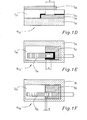
- Fig. 1D shows still another known parallel-plate, varactor arrangement 10 04 comprising a substrate 1 04 , a top electrode 3 04' and a bottom electrode 3 04 which are disposed on either sides of a ferroelectric film 2 04 such as to partly overlap.
- a low permittivity film (with dielectric constant ⁇ 10) 4 04 is arranged such as to define the overlapping area, the length portion b where there is no such extra film defining the actual relevant portion.
- a top view of this arrangement is shown in Fig. 1E where it can be seen the width c of the overlapping portion and hence the overlapping area being defined by the opening b ⁇ c in the low permittivity film.
- varactors with coplanar plate electrodes as shown in Fig. 1A have a simple design but they require application of higher voltages than parallel-plate varactor arrangements, typically the required voltage is above 50-100V.
- Varactors with parallel-plate electrodes as shown in Fig. 1B-1C do not require such high voltages but typically it is enough with a voltage of 5-20V, but on the other hand it is a disadvantage of such designs that they are sensitive to the alignment of the top and the bottom electrodes during the fabrication process.
- a ferroelectric film with an extremely high permittivity is used and due to this extremely high permittivity, which typically is above 100, a small disalignment ⁇ l (c.f. Fig.
- a capacitance arrangement for which the capacitance can be predicted to a high extent.
- a capacitance arrangement is needed which has a simple design and which still does not require, particularly in the case of a varactor arrangement, high voltages.
- a capacitance arrangement or varactor arrangement is needed which to a high degree is insensitive to any misalignment.
- a capacitance arrangement or a varactor arrangement is needed through which the capacitance is controllable.
- a varactor arrangement is needed which is easy and cost efficient to fabricate.
- Still further such a capacitance arrangement is needed which does not suffer from high ohmic losses due to the design.
- a capacitance arrangement is needed which has low ohmic losses or a high Q-factor associated with the electrodes and which does not require many masks and processing steps hence enabling a cost effective fabrication.
- a parallel-plate varactor or capacitance arrangement is needed for which the effective overlap area is not sensitive to any misalignment that may. be introduced during the fabrication.
- a capacitance arrangement as initially referred to is provided wherein a first electrode means comprises a first and a second electrode arranged symmetrically with respect to a longitudinal axis. Said first and second electrodes have a respective first edge, which respective first edges face each other, are linear and parallel such that a gap is defined there between.
- the second electrode means comprises a third electrode which comprises a first section and a second section disposed on opposite sides of said gap and inter-connected by means of an intermediate section which is delimited by a first curved edge and a second curved edge. Said first and second curved edges are symmetrical and oppositely directed with respect to said longitudinal axis.
- the shape of said intermediate section is given by a function F(x) which contains a first parameter and a second parameter.
- One of said parameters is adapted to be selected, allowing calculation of the other parameter such that the capacitance of the capacitance arrangement will be misalignment invariable within the given misalignment limit.
- the said first parameter (k) determines the shape or the curvature of F(x) (and size) and the second parameter (A) is half the width of the second electrode means, i.e. the third electrode.
- the first parameter k is adapted to be selected allowing calculation of the second parameter A which normally is easier.
- the inventive concept also covers the case wherein the second parameter is selected and the first parameter calculated depending on said selection.
- the first and second electrodes are adapted to have a shape and to be arranged such that the overlapping area gives a predetermined capacitance independently of any occurring misalignment ( ⁇ x) within the given misalignment limit giving different overlaps in the region of the intermediate section on the side of the first section and of the second section, i.e. the overlapping area will not be symmetric with respect to an axis perpendicular to the longitudinal axis in the middle of the first and second electrode.
- the capacitance between the first electrode and the third electrode is proportional to the sum of the overlap of the first electrode and the first section of the third electrode, the overlap between the first electrode and the intermediate section in the absence of any misalignment, and the first misalignment overlap area ( ⁇ S 1 ), wherein the first electrode and the intermediate section in the longitudinal direction limited by the maximum allowed misalignment.
- the capacitance between the second electrode and the third electrode is proportional to the sum of the overlapping area of the second electrode and the second section of the third electrode, the overlap between the second electrode and the intermediate section in absence of any misalignment and a second misalignment overlapping area ( ⁇ S 2 ) of the second electrode and the intermediate section in the opposite longitudinal direction limited by the maximum allowed misalignment.
- first and second misalignment overlapping areas have opposite signs, i.e. if the first misalignment overlapping area has a positive sign, the second has a negative sign or vice versa.
- first and second parameters are so selected and calculated respectively that the relationship between the first and the second misalignment overlap areas, ⁇ S 1 , ⁇ S 2 , or between corresponding first and second capacitance differences ⁇ C 1 , ⁇ C 2 , will be such that the equivalent capacitance of the arrangement is independent of any produced misalignment, within the given misalignment limit.
- the first and second sections are symmetrical.
- the first and second sections may be square shaped, rectangular, semicircular or partly irregular.
- the second electrode means comprises a bottom electrode and the first electrode means comprises a top electrode, or vice versa.
- the first or the second electrode means may be disposed on a substrate although this is not necessarily the case.
- the dielectric material has a low or comparatively low dielectric constant, for example consisting of SiO 2 or a material with similar properties, the arrangement being a non-tunable capacitance arrangement.
- the dielectric layer comprises a ferroelectric layer with a tunable dielectric constant which preferably is high or very high.
- the dielectric layer may then for example comprise a tunable ceramic material such as SrTiO 3 , BaSTO or a material with similar properties.
- the electrode means generally consists of a metal such as Au, Ag, Pt, Cu.
- the ferroelectric or dielectric material may comprise a thin film, i.e. thin film technology may be implemented.
- the invention is not limited to thin film implementations but the dielectric or ferroelectric layer may also comprise a thick film.
- circuits particularly capacitors or varactors
- circuits can be fabricated having precisely or accurately defined capacitance values.
- parallel plate capacitors or varactors which are, to a high degree, insensitive to misalignments between the top and bottom electrodes that may be produced during the fabrication process.
- the top and/or bottom electrodes are so shaped in relation to each other that the effective overlapping area will be unsensitive to any misalignment (within a predetermined maximum misalignment limit).
- the arrangements according to the different embodiments can be made as capacitance arrangements or as varactor arrangements, i.e. comprising a tunable capacitor.
- varactors i.e. comprising a tunable capacitor.
- it may just as well be capacitors, the difference lying in the dielectric constant of the thin or thick film on either sides of which first and second electrode means are disposed.
- Fig. 2 shows a first embodiment of a varactor arrangement 10 according to the present invention.
- the lay-out is presented for a case where there actually is no misalignment between the electrodes on either sides of the ferroelectric layer.
- a first electrode means comprising a first electrode 4 1 and a second electrode 4 2 are disposed on a thin ferroelectric film (not shown in the figure). It is here supposed that the first and second electrodes 4 1 , 4 2 are rectangular or square shaped and disposed symmetrically with respect to a longitudinal axis x such that a gap of a width w g is provided between them.
- a second electrode means comprising a third electrode 3 is disposed on the other side of the ferroelectric film. It comprises a first electrode section 3 1 and a second electrode section 3 2 which have the same shape and which here also are supposed to be symmetrically disposed with respect to the longitudinal axis x. In this particular embodiment they are supposed to be square shaped but they may have substantially any shape as will be shown below.
- An intermediate section 3 3 interconnects said first and second sections 3 1 , 3 2 .
- the shape of the intermediate section 3 3 is determined by a function F(x) which is to be appropriately established as will be more thoroughly described below.
- the equivalent capacitance of the arrangement is given by the overlapping areas which here are the same, i.e. the part of the first and second electrodes 4 1 , 4 2 overlapping first and second sections 3 1 , 3 2 of the second electrode means and, since there is no misalignment, the symmetrical and identical overlapping areas of the intermediate section 3 3 and the first and second electrodes 4 1 , 4 2 .
- two metallized interfaces comprising the first and second electrode means 4 1 , 4 2 , 3 are precisely aligned forming the varactor 10, established by a series connection of two similar varactors, c.f.
- Fig. 2A is a simplified circuit representation of a first varactor comprising the varactor formed by the overlapping area between the first electrode 4 1 and the first section 3 1 of the third electrode 3 and part of the intermediate section 3 3 connected to the first section 3 1 identical to the area S1 and correspondingly C2 is the capacitance of the varactor formed by the second electrode 4 2 and the second section 3 2 and the corresponding part of the intermediate section 3 3 connected to said second section. In this case they are identical.
- Fig. 3 shows the topology of the same arrangement as in Fig. 2 but where there is a misalignment ⁇ x between the first and the second electrode means. As can be seen from the figure, the effect of the misalignment will differ for the two varactors.
- ⁇ x illustrates the misalignment.
- the first electrode means comprising the electrodes 4 1 and 4 2 has been displaced a distance ⁇ x on the longitudinal axis x.
- the misalignment area also called the capacitance area of the first varactor is increased, the increase being indicated ⁇ S1 in the figure, and C1 ⁇ S1+ ⁇ S1.
- the capacitance is decreased by ⁇ C2, i.e. C2 ⁇ S1- ⁇ S2, which means that for the first varactor, in this case, the capacitance is increased whereas it for the other is decreased.
- ⁇ S1 indicates the misalignment area for the first varactor
- ⁇ S2 indicates the misalignment area for the second varactor.
- ⁇ S1 is not equal to ⁇ S2.
- the relationship between ⁇ C1 and ⁇ C2 is established so that the total capacitance or equivalent capacitance of the misalignment capacitor is the same as the total capacitance without misalignment, i.e. it should be the same for the varactor arrangement of Fig. 2 as for the varactor arrangement of Fig. 3 .
- A kS ⁇ 1 / 2 ⁇ e kWg / 2 .
- 2A corresponds to the width of the second electrode means.
- Fig. 8 is a figure similar to Fig. 7 for another design where the electrodes or particularly the first and second electrodes sections of the second electrodes means are of a more general shape instead of rectangular though their areas are similar.
- Fig. 4 is a figure similar to Fig. 3 showing a varactor arrangement 20 where a second electrode means 3' comprising a first electrode section 3 1 ' and a second electrode section 3 2 ' connected by an intermediate section 3 3 ' arranged on a substrate 1' on top of which of a dielectrical ferroelectric film is arranged, upon which a first electrode means comprising a first electrode 4 1 ' and a second electrode 4 2 ' is disposed such that an overlap is given corresponding to S1'+ ⁇ S1' and S2'- ⁇ S2' respectively.
- ⁇ x since there is a misalignment present, ⁇ x, the misalignment areas ⁇ S 1 ' and ⁇ S 2 ' are not the same (cf. Fig. 3 ).
- the difference actually here is that the first and second electrode sections 3 1 ', 3 2 ' are substantially semicircular, or have an oval shape.
- Fig. 5 shows still another embodiment of a varactor arrangement 30 wherein a second electrode means comprising a first electrode section 3 1 " and a second electrode section 3 2 " interconnected by means of a intermediate section 3 3 " is disposed on a substrate arranged such as to provide an overlap with a first electrode means comprising a first and a second electrode 4 1 ", 4 2 " which sections are rectangular and arranged as the structure in Fig. 2 , i.e. symmetrically along a longitudinal axis x but with a misalignment where the misalignment area ⁇ S 1 " and ⁇ S 2 " are not equal.
- the first and second electrode sections are rectangular instead of semicircular or squareshaped or similar.
- the functioning is the same as that described with reference to Fig. 2 and 3 and the figure is merely included to explicitely illustrate that different shapes can be used.
- Fig. 6 very schematically shows a varactor arrangement 40 comprising two varactors 3 10 , 3 20 , 30 30 connected in series.
- this figure is very schematical, the only intention thereof being to illustrate that several capacitors formed by first and second electrode means as discussed above, etc. can be used which are arranged to provide a misalignment invariable arrangement.
Landscapes
- Engineering & Computer Science (AREA)
- Power Engineering (AREA)
- Microelectronics & Electronic Packaging (AREA)
- Manufacturing & Machinery (AREA)
- Fixed Capacitors And Capacitor Manufacturing Machines (AREA)
- Ceramic Capacitors (AREA)
- Supplying Of Containers To The Packaging Station (AREA)
- Making Paper Articles (AREA)
Claims (15)
- Kapazitätsanordnung (10; 20; 30; 40), die wenigstens einen Parallelplattenkondensator umfasst, der Folgendes umfasst: eine erste Elektrodeneinheit (41, 42; 41', 42'; 41", 42"; 310, 320, 330), eine dielektrische Schicht und eine zweite Elektrodeneinheit (3, 3'; 3"; 410, 420, 430), die im Wesentlichen parallel auf beiden Seiten der dielektrischen Schicht und einander teilweise überlappend angeordnet sind, wobei die äquivalente Kapazität der Kapazitätsanordnung von der Größe des Überlappungsbereichs der ersten und der zweiten Elektrodeneinheit abhängig ist, und wobei ein Fehlausrichtungslimit vorgegeben wird, das das maximal zulässige Ausmaß an Fehlausrichtung (Δχ4) zwischen einer jeweiligen ersten und zweiten Elektrodeneinheit definiert,
dadurch gekennzeichnet,
dass die erste Elektrodeneiheit (41, 42; 41', 42'; 41", 42"; 310, 320, 330) eine erste und eine zweite Elektrode umfasst, die symmetrisch mit Bezug auf eine Längsachse (x) angeordnet sind, dass die erste und die zweite Elektrode (41, 42; 41', 42'; 41", 42"; 310, 320, 330) einen jeweiligen ersten Rand haben, wobei die jeweiligen ersten Ränder einander zugewandt sind, linear und parallel sind, so dass eine Lücke dazwischen definiert wird, dass die zweite Elektrodeneinheit (3, 3'; 3"; 410, 420, 430) eine dritte Elektrode umfasst, wobei die dritte Elektrode eine erste Sektion (31, 31'; 31") und eine zweite Sektion (32, 32'; 32") umfasst, die auf gegenüberliegenden Seiten der Lücke angeordnet und durch eine Zwischensektion (33, 33'; 33") verbunden sind, der durch einen ersten gekrümmten Rand und einen zweiten gekrümmten Rand begrenzt werden, wobei der erste und der zweite gekrümmte Rand mit Bezug auf die Längsachse symmetrisch und entgegengesetzt gerichtet sind,
und deren Form durch eine Funktion F(x) in Abhängigkeit von einem ersten Parameter k und einem zweiten Parameter A vorgegeben wird, und dadurch, dass einer der beiden Parameter angepasst ist, um ausgewählt zu werden, so dass der andere Parameter berechnet werden kann, um Form und Größe der zweiten Elektrodeneinheit (3, 3'; 3"; 410, 420, 430) zu bestimmen, so dass die Kapazität der Kapazitätsanordnung durch eine Fehlausrichtung innerhalb des Fehlausrichtungslimits nicht verändert wird. - Kapazitätsanordnung nach Anspruch 1, dadurch gekennzeichnet, dass der erste Parameter (k) Form oder Krümmung von F(x) bestimmt, und dadurch, dass der zweite Parameter (A) die Hälfte der Breite (2A) der zweiten Elektrodeneinheit halt, d.h. die dritte Elektrode.
- Kapazitätsanordnung nach Anspruch 2, dadurch gekennzeichnet, dass der erste Parameter (k) angepasst ist, um ausgewählt zu werden, so dass der zweite Parameter (A) berechnet werden kann.
- Kapazitätsanordnung nach einem der vorherigen Ansprüche, dadurch gekennzeichnet, dass die erste und die zweite Elektrode angepasst sind, um eine Form zu haben und angeordnet zu sein, so dass der Überlappungsbereich eine vorbestimmte Kapazität unabhängig von einer Fehlausrichtung Δχ innerhalb des gegebenen Fehlausrichtungslimits ΔχA bei unterschiedlichen Überlappungen der ersten Elektrodeneinheit und der Zwischensektion (33, 33'; 33") auf der Seite der ersten Sektion und der zweiten Sektion ergibt.
- Kapazitätsanordnung nach einem der Ansprüche 1 bis 4, dadurch gekennzeichnet, dass die Kapazität zwischen der ersten Elektrode und der dritten Elektrode proportional zur Summe der Überlappung der ersten Elektrode und der ersten Sektion der dritten Elektrode, der Überlappung zwischen der ersten Elektrode und der Zwischensektion in Anwesenheit einer Fehlausrichtung und eines ersten Fehlausrichtungsüberlappungsbereichs (ΔS1) ist, wobei die erste Elektrode und die Zwischensektion in der Längsrichtung durch die maximal zulässig Fehlausrichtung Δx begrenzt werden, und dadurch, dass die Kapazität zwischen der zweiten Elektrode und der dritten Elektrode proportional zur Summe des Überlappungsbereichs der zweiten Elektrode und der zweiten Sektion der dritten Elektrode und der Überlappung zwischen der zweiten Elektrode und der Zwischensektion in Abwesenheit einer Fehlausrichtung ist, und wobei ein zweiter Fehlerausrichtungsüberlappungsbereich (ΔS2) der zweiten Elektrode und der Zwischensektion in der entgegengesetzten Längsrichtung durch die maximal zulässige Fehlausrichtung begrenzt wird, wobei der erste und der zweite Fehlausrichtungsüberlappungsbereich entgegengesetzte Vorzeichen haben, d.h. wenn der erste Fehlausrichtungsüberlappungsbereich ein positives Vorzeichen hat, dann hat der zweite ein negatives Vorzeichen, oder umgekehrt.
- Kapazitätsanordnung nach Anspruch 5, dadurch gekennzeichnet, dass der erste und der zweite Parameter jeweils so gewählt und berechnet werden, dass die Beziehung zwischen dem ersten und dem zweiten Fehlausrichtungsüberlappungsbereich (ΔS1, ΔS2) oder zwischen entsprechenden einer ersten und einer zweiten Kapazitätsdifferenz (ΔC1, ΔC2) derart ist, dass die äquivalente Kapazität der Anordnung von einer Fehlausrichtung innerhalb des gegebenen Fehlausrichtungslimits unabhängig ist.
- Kapazitätsanordnung nach Anspruch 5, dadurch gekennzeichet, dass der erste Fehlerausrichtungsüberlappungsbereich (ΔS1) gleich dem Überlappungsbereich einer ersten oder zweiten Elektrode und einer ersten oder zweiten Elektrodensektion der zweiten Elektrodeneinheit in Abwesenheit von Fehlausrichtungen (S1) dividiert durch den Quotienten zwischen dem Überlappungsbereich und dem zweiten Fehlausrichtungsbereich (S1/ΔS2) minus 2 ist, d.h. ΔS1=S1/((S1/ΔS1)-2).
- Kapazitätsanordnung nach einem der vorherigen Ansprüche, dadurch gekennzeichnet, dass die Form der Zwischensektion durch F(x)=A·ekx angegeben wird, wobei 2A die Breite der zweiten Elektrodeneinheit ist, d.h. das Zweifache des zweiten Parameters, und wobei k der erste Parameter ist, der die Neigung oder Krümmung definiert, wobei 0<x<2 ΔxA ist, wobei ΔxA das Fehlausrichtungslimit ist.
- Kapazitätsanordnung nach einem der vorherigen Ansprüche, dadurch gekennzeichnet, dass die Hälfte der Breite der zweiten Elektrodeneinheit A= k·S1/(ek·Wg/2) beträgt, wobei S1 der Überlappungsbereich einer ersten/zweiten Elektrode
und einer ersten/zweiten Elektrodensektion in Abwesenheit einer Fehlausrichtung ist, wobei Wg die Lückenbreite und k der erste Parameter ist, der die Neigung oder Krümmung der Funktion bestimmt, die die Zwischensektion (33, 33'; 33") begrenzt. - Kapazitätsanordnung nach einem der vorherigen Ansprüche, dadurch gekennzeichnet, dass das dielektrische Material eine niedrige Dielektrizitätskonstante hat.
- Kapazitätsanordnung nach einem der Ansprüche 1 bis 9, dadurch gekennzeichnet, dass sie eine Varaktoranordnung oder eine Anzahl von in Reihe geschalteten parallelen Plattenkondensatoren oder Varaktoren umfasst.
- Kapazitätsanordnung nach Anspruch 11, dadurch gekennzeichnet, dass die dielektrische Schicht eine ferroelektrische Schicht mit einer abstimmbaren Dielektrizitätskonstante umfasst, die vorzugsweise hoch oder sehr hoch ist, oder dass die dielektrische Schicht ein abstimmbares Keramikmaterial SrTiO3, Ba STO oder ein Material mit ähnlichen Eigenschaften umfasst.
- Kapazitätsanordnung nach einem der vorherigen Ansprüche, dadurch gekennzeichnet, dass das ferroelektrische Material einen Dünnfilm umfasst oder dass die dielektrische oder ferroelektrische Schicht einen Dickfilm umfasst und dass die erste und die zweite Elektrodeneinheit aus einem Metall wie Au, Ag, Pt, Cu bestehen.
- Verfahren zum Erzeugen einer Kapazitätsanordnung, die wenigstens einen Parallelplattenkondensator umfasst, der Folgendes umfasst: eine erste Elektrodeneinheit, eine dielektrische Schicht und eine zweite Elektrodeneinheit, wobei die erste und die zweite Elektrodeneinheit einander teilweise überlappen, wobei die Größe des Überlappungsbereichs die äquivalente Kapazität der Anordnung ergibt und wobei ferner ein zulässiges Fehlausrichtungslimit gegeben wird, das das maximal zulässig Ausmaß an Fehlausrichtung zwischen einer jeweiligen ersten und zweiten Elektrode definiert,
dadurch gekennzeichnet, dass es die folgenden Schritte beinhaltet:- Bewirken, dass eine äquivalente Kapazität bereitgestellt wird,- Ermitteln eines zulässigen Fehlausrichtungslimits,- Konstruieren einer ersten Elektrodeneinheit, die zwei im Wesentlichen symmetrische Elektroden mit zwei jeweiligen Rändern umfasst, die einander zugewandt, linear, parallel und angepasst sind, um symmetrisch auf einer Längsachse angeordnet zu sein, so dass eine Lücke dazwischen entsteht, und einer zweiten Elektrodeneinheit, die eine dritte Elektrode umfasst, die eine erste und eine zweite Sektion umfasst, die sich auf gegenüberliegenden Seiten der Lücke befinden und durch eine Zwischensektion miteinander verbunden sind, durch Finden einer Funktion F(x), die von einem ersten Parameter k und einem zweiten Parameter A abhängig ist und in der Längsachse (-F(x)) gespiegelt ist, die die Form der Zwischensektion auf den gegenüberliegenden Seite der Längsachse bestimmt, so dass die äquivalente Kapazität durch eine Fehlausrichtung innerhalb der Fehlausrichtungsgrenzen nicht verändert wird. - Verfahren nach Anspruch 14, dadurch gekennzeichnet, dass der erste Parameter (k) die Krümmungsform von F(x) bestimmt, und dadurch, dass der zweite Parameter (A) die Hälfte der Breite (2A) der zweiten E!ektrodeneinheit beträgt, und dadurch, dass das Verfahren die folgenden Schritte beinhaltet:- Auswählen des Wertes von einem der Parameter;- Berechnen des Wertes des anderen der Parameter anhand des ausgewählten Parameterwertes; und- Anordnen der ersten und der zweiten Elektrodeneinheit auf beiden Seiten einer dielektrischen Schicht, oder- Anordnen der ersten und der zweiten Elektrodeneinheit auf beiden Seiten einer ferroelekirischen Schicht mit einer variablen Dielektrizitätskonstante, um eine Varaktoranordnung bereitzustellen.
Applications Claiming Priority (1)
| Application Number | Priority Date | Filing Date | Title |
|---|---|---|---|
| PCT/EP2006/067347 WO2008043395A1 (en) | 2006-10-12 | 2006-10-12 | Capacitance arrangement and method relating thereto |
Publications (2)
| Publication Number | Publication Date |
|---|---|
| EP2074640A1 EP2074640A1 (de) | 2009-07-01 |
| EP2074640B1 true EP2074640B1 (de) | 2010-12-08 |
Family
ID=38059036
Family Applications (1)
| Application Number | Title | Priority Date | Filing Date |
|---|---|---|---|
| EP06807212A Not-in-force EP2074640B1 (de) | 2006-10-12 | 2006-10-12 | Kapazitätsanordnung und verfahren zu ihrer herstellung |
Country Status (7)
| Country | Link |
|---|---|
| US (1) | US8009406B2 (de) |
| EP (1) | EP2074640B1 (de) |
| CN (1) | CN101523527B (de) |
| AT (1) | ATE491215T1 (de) |
| DE (1) | DE602006018802D1 (de) |
| ES (1) | ES2357555T3 (de) |
| WO (1) | WO2008043395A1 (de) |
Families Citing this family (3)
| Publication number | Priority date | Publication date | Assignee | Title |
|---|---|---|---|---|
| JP2014146676A (ja) * | 2013-01-29 | 2014-08-14 | Murata Mfg Co Ltd | 可変容量コンデンサ |
| US9750282B2 (en) * | 2014-09-12 | 2017-09-05 | Shenzhen Smoore Technology Limited | Electronic cigarette and air switch thereof |
| JP7389219B2 (ja) | 2019-10-30 | 2023-11-29 | 京東方科技集團股▲ふん▼有限公司 | アレイ基板及び表示装置 |
Family Cites Families (12)
| Publication number | Priority date | Publication date | Assignee | Title |
|---|---|---|---|---|
| US5699224A (en) * | 1995-10-25 | 1997-12-16 | Rohm Co., Ltd. | Thick-film capacitor and chip-type composite electronic component utilizing the same |
| JPH09120933A (ja) * | 1995-10-25 | 1997-05-06 | Rohm Co Ltd | 厚膜コンデンサ |
| JP3606164B2 (ja) * | 2000-06-02 | 2005-01-05 | 株式会社村田製作所 | 静電容量型外力検出装置 |
| US6377440B1 (en) * | 2000-09-12 | 2002-04-23 | Paratek Microwave, Inc. | Dielectric varactors with offset two-layer electrodes |
| SE520018C2 (sv) * | 2001-05-09 | 2003-05-06 | Ericsson Telefon Ab L M | Ferroelektriska anordningar och förfarande relaterande därtill |
| US20040259316A1 (en) * | 2001-12-05 | 2004-12-23 | Baki Acikel | Fabrication of parallel plate capacitors using BST thin films |
| US6785117B2 (en) * | 2002-03-15 | 2004-08-31 | Denso Corporation | Capacitive device |
| AU2003243546A1 (en) * | 2002-06-13 | 2003-12-31 | Wispry, Inc. | Micro-electro-mechanical system (mems) variable capacitor apparatuses and related methods |
| US6556415B1 (en) * | 2002-06-28 | 2003-04-29 | Industrial Technologies Research Institute | Tunable/variable passive microelectronic components |
| US7372346B2 (en) * | 2003-12-24 | 2008-05-13 | Interuniversitair Microelektronica Centrum (Imec) | Acoustic resonator |
| EP1548935A1 (de) * | 2003-12-24 | 2005-06-29 | Interuniversitair Microelektronica Centrum Vzw | Mikrostrukturierter Dünnfilmresonator |
| FR2876215B1 (fr) * | 2004-10-04 | 2007-05-11 | Commissariat Energie Atomique | Capacite variable a fluide dielectrique |
-
2006
- 2006-10-12 ES ES06807212T patent/ES2357555T3/es active Active
- 2006-10-12 WO PCT/EP2006/067347 patent/WO2008043395A1/en not_active Ceased
- 2006-10-12 EP EP06807212A patent/EP2074640B1/de not_active Not-in-force
- 2006-10-12 CN CN2006800560878A patent/CN101523527B/zh not_active Expired - Fee Related
- 2006-10-12 DE DE602006018802T patent/DE602006018802D1/de active Active
- 2006-10-12 AT AT06807212T patent/ATE491215T1/de not_active IP Right Cessation
- 2006-10-12 US US12/444,819 patent/US8009406B2/en not_active Expired - Fee Related
Also Published As
| Publication number | Publication date |
|---|---|
| ES2357555T3 (es) | 2011-04-27 |
| ATE491215T1 (de) | 2010-12-15 |
| CN101523527A (zh) | 2009-09-02 |
| EP2074640A1 (de) | 2009-07-01 |
| US8009406B2 (en) | 2011-08-30 |
| DE602006018802D1 (de) | 2011-01-20 |
| CN101523527B (zh) | 2011-09-14 |
| WO2008043395A1 (en) | 2008-04-17 |
| US20100006981A1 (en) | 2010-01-14 |
Similar Documents
| Publication | Publication Date | Title |
|---|---|---|
| EP1224675B1 (de) | Durchstimmbarer hochfrequenz-kondensator | |
| US8174341B2 (en) | Thin film based split resonator tunable metamaterial | |
| DE69621011T2 (de) | Kondensator für eine integrierte schaltung | |
| DE69228146T2 (de) | Verbesserte Miniatur-Abstimmschaltung für Mikrowellen und Millimeterwellen | |
| WO2001045120A3 (en) | Variable capacitor and associated fabrication method | |
| DE69612576T2 (de) | Mikrobearbeiteter symmetrischer Differentialdrucksensor mit Polysilizium | |
| DE69108608T3 (de) | Kapazitiver Beschleunigungsaufnehmer mit freier Membran. | |
| DE102014214154A1 (de) | Ein MEMS-Bauelement | |
| JPH0410406A (ja) | 積層コンデンサ | |
| DE102004043259B4 (de) | Dynamischer Halbleitersensor mit variablem Kondensator auf laminiertem Substrat | |
| EP3991203B1 (de) | Kapazitätsstruktur | |
| DE10141867B4 (de) | Halbleitersensor für dynamische Grössen mit beweglichen Elektroden und Festelektroden auf einem Unterstützungssubstrat | |
| DE112019006862B4 (de) | Piezoelektrisches Bauelement | |
| EP2074640B1 (de) | Kapazitätsanordnung und verfahren zu ihrer herstellung | |
| DE60203021T2 (de) | Mikroeinstellbarer kondensator (mems) mit weitem variationsbereich und niedriger betätigungsspannung | |
| DE10137121A1 (de) | Piezoelektrischer Oszillator | |
| DE10335331A1 (de) | Elektrisches Bauelement mit überlappenden Elektroden und Verfahren zur Herstellung | |
| DE102007024901A1 (de) | Kondensatorstruktur mit veränderbarer Kapzität und Verwendung der Kondensatorstruktur | |
| DE19814688A1 (de) | Chip-artiges piezoelektrisches Filter | |
| US11894190B2 (en) | Electrical component | |
| US7158363B2 (en) | Liquid metal varactor and method | |
| US5291162A (en) | Method of adjusting frequency response in a microwave strip-line filter device | |
| EP2590190B1 (de) | Dünnfilmkondensatoren | |
| DE69816737T2 (de) | Herstellungsverfahren für piezoelektrischen Resonator | |
| EP1024508A2 (de) | Elektrostatisch durchstimmbare Kapazität |
Legal Events
| Date | Code | Title | Description |
|---|---|---|---|
| PUAI | Public reference made under article 153(3) epc to a published international application that has entered the european phase |
Free format text: ORIGINAL CODE: 0009012 |
|
| 17P | Request for examination filed |
Effective date: 20090409 |
|
| AK | Designated contracting states |
Kind code of ref document: A1 Designated state(s): AT BE BG CH CY CZ DE DK EE ES FI FR GB GR HU IE IS IT LI LT LU LV MC NL PL PT RO SE SI SK TR |
|
| AX | Request for extension of the european patent |
Extension state: AL BA HR MK RS |
|
| GRAP | Despatch of communication of intention to grant a patent |
Free format text: ORIGINAL CODE: EPIDOSNIGR1 |
|
| RTI1 | Title (correction) |
Free format text: CAPACITANCE ARRANGEMENT AND METHOD FOR PRODUCING IT |
|
| DAX | Request for extension of the european patent (deleted) | ||
| GRAS | Grant fee paid |
Free format text: ORIGINAL CODE: EPIDOSNIGR3 |
|
| GRAA | (expected) grant |
Free format text: ORIGINAL CODE: 0009210 |
|
| AK | Designated contracting states |
Kind code of ref document: B1 Designated state(s): AT BE BG CH CY CZ DE DK EE ES FI FR GB GR HU IE IS IT LI LT LU LV MC NL PL PT RO SE SI SK TR |
|
| REG | Reference to a national code |
Ref country code: GB Ref legal event code: FG4D |
|
| REG | Reference to a national code |
Ref country code: CH Ref legal event code: EP |
|
| REG | Reference to a national code |
Ref country code: IE Ref legal event code: FG4D |
|
| REF | Corresponds to: |
Ref document number: 602006018802 Country of ref document: DE Date of ref document: 20110120 Kind code of ref document: P |
|
| REG | Reference to a national code |
Ref country code: NL Ref legal event code: VDEP Effective date: 20101208 |
|
| REG | Reference to a national code |
Ref country code: ES Ref legal event code: FG2A Ref document number: 2357555 Country of ref document: ES Kind code of ref document: T3 Effective date: 20110427 |
|
| PG25 | Lapsed in a contracting state [announced via postgrant information from national office to epo] |
Ref country code: LT Free format text: LAPSE BECAUSE OF FAILURE TO SUBMIT A TRANSLATION OF THE DESCRIPTION OR TO PAY THE FEE WITHIN THE PRESCRIBED TIME-LIMIT Effective date: 20101208 |
|
| LTIE | Lt: invalidation of european patent or patent extension |
Effective date: 20101208 |
|
| PG25 | Lapsed in a contracting state [announced via postgrant information from national office to epo] |
Ref country code: AT Free format text: LAPSE BECAUSE OF FAILURE TO SUBMIT A TRANSLATION OF THE DESCRIPTION OR TO PAY THE FEE WITHIN THE PRESCRIBED TIME-LIMIT Effective date: 20101208 Ref country code: CY Free format text: LAPSE BECAUSE OF FAILURE TO SUBMIT A TRANSLATION OF THE DESCRIPTION OR TO PAY THE FEE WITHIN THE PRESCRIBED TIME-LIMIT Effective date: 20101208 Ref country code: BG Free format text: LAPSE BECAUSE OF FAILURE TO SUBMIT A TRANSLATION OF THE DESCRIPTION OR TO PAY THE FEE WITHIN THE PRESCRIBED TIME-LIMIT Effective date: 20110308 Ref country code: LV Free format text: LAPSE BECAUSE OF FAILURE TO SUBMIT A TRANSLATION OF THE DESCRIPTION OR TO PAY THE FEE WITHIN THE PRESCRIBED TIME-LIMIT Effective date: 20101208 Ref country code: SI Free format text: LAPSE BECAUSE OF FAILURE TO SUBMIT A TRANSLATION OF THE DESCRIPTION OR TO PAY THE FEE WITHIN THE PRESCRIBED TIME-LIMIT Effective date: 20101208 Ref country code: SE Free format text: LAPSE BECAUSE OF FAILURE TO SUBMIT A TRANSLATION OF THE DESCRIPTION OR TO PAY THE FEE WITHIN THE PRESCRIBED TIME-LIMIT Effective date: 20101208 Ref country code: FI Free format text: LAPSE BECAUSE OF FAILURE TO SUBMIT A TRANSLATION OF THE DESCRIPTION OR TO PAY THE FEE WITHIN THE PRESCRIBED TIME-LIMIT Effective date: 20101208 Ref country code: NL Free format text: LAPSE BECAUSE OF FAILURE TO SUBMIT A TRANSLATION OF THE DESCRIPTION OR TO PAY THE FEE WITHIN THE PRESCRIBED TIME-LIMIT Effective date: 20101208 |
|
| PG25 | Lapsed in a contracting state [announced via postgrant information from national office to epo] |
Ref country code: CZ Free format text: LAPSE BECAUSE OF FAILURE TO SUBMIT A TRANSLATION OF THE DESCRIPTION OR TO PAY THE FEE WITHIN THE PRESCRIBED TIME-LIMIT Effective date: 20101208 Ref country code: EE Free format text: LAPSE BECAUSE OF FAILURE TO SUBMIT A TRANSLATION OF THE DESCRIPTION OR TO PAY THE FEE WITHIN THE PRESCRIBED TIME-LIMIT Effective date: 20101208 Ref country code: PT Free format text: LAPSE BECAUSE OF FAILURE TO SUBMIT A TRANSLATION OF THE DESCRIPTION OR TO PAY THE FEE WITHIN THE PRESCRIBED TIME-LIMIT Effective date: 20110408 Ref country code: BE Free format text: LAPSE BECAUSE OF FAILURE TO SUBMIT A TRANSLATION OF THE DESCRIPTION OR TO PAY THE FEE WITHIN THE PRESCRIBED TIME-LIMIT Effective date: 20101208 Ref country code: IS Free format text: LAPSE BECAUSE OF FAILURE TO SUBMIT A TRANSLATION OF THE DESCRIPTION OR TO PAY THE FEE WITHIN THE PRESCRIBED TIME-LIMIT Effective date: 20110408 Ref country code: GR Free format text: LAPSE BECAUSE OF FAILURE TO SUBMIT A TRANSLATION OF THE DESCRIPTION OR TO PAY THE FEE WITHIN THE PRESCRIBED TIME-LIMIT Effective date: 20110309 |
|
| PG25 | Lapsed in a contracting state [announced via postgrant information from national office to epo] |
Ref country code: PL Free format text: LAPSE BECAUSE OF FAILURE TO SUBMIT A TRANSLATION OF THE DESCRIPTION OR TO PAY THE FEE WITHIN THE PRESCRIBED TIME-LIMIT Effective date: 20101208 Ref country code: RO Free format text: LAPSE BECAUSE OF FAILURE TO SUBMIT A TRANSLATION OF THE DESCRIPTION OR TO PAY THE FEE WITHIN THE PRESCRIBED TIME-LIMIT Effective date: 20101208 Ref country code: SK Free format text: LAPSE BECAUSE OF FAILURE TO SUBMIT A TRANSLATION OF THE DESCRIPTION OR TO PAY THE FEE WITHIN THE PRESCRIBED TIME-LIMIT Effective date: 20101208 |
|
| PLBE | No opposition filed within time limit |
Free format text: ORIGINAL CODE: 0009261 |
|
| STAA | Information on the status of an ep patent application or granted ep patent |
Free format text: STATUS: NO OPPOSITION FILED WITHIN TIME LIMIT |
|
| PG25 | Lapsed in a contracting state [announced via postgrant information from national office to epo] |
Ref country code: DK Free format text: LAPSE BECAUSE OF FAILURE TO SUBMIT A TRANSLATION OF THE DESCRIPTION OR TO PAY THE FEE WITHIN THE PRESCRIBED TIME-LIMIT Effective date: 20101208 |
|
| 26N | No opposition filed |
Effective date: 20110909 |
|
| PG25 | Lapsed in a contracting state [announced via postgrant information from national office to epo] |
Ref country code: IT Free format text: LAPSE BECAUSE OF FAILURE TO SUBMIT A TRANSLATION OF THE DESCRIPTION OR TO PAY THE FEE WITHIN THE PRESCRIBED TIME-LIMIT Effective date: 20101208 |
|
| REG | Reference to a national code |
Ref country code: DE Ref legal event code: R097 Ref document number: 602006018802 Country of ref document: DE Effective date: 20110909 |
|
| PG25 | Lapsed in a contracting state [announced via postgrant information from national office to epo] |
Ref country code: MC Free format text: LAPSE BECAUSE OF NON-PAYMENT OF DUE FEES Effective date: 20111031 |
|
| REG | Reference to a national code |
Ref country code: CH Ref legal event code: PL |
|
| REG | Reference to a national code |
Ref country code: FR Ref legal event code: ST Effective date: 20120629 |
|
| PG25 | Lapsed in a contracting state [announced via postgrant information from national office to epo] |
Ref country code: LI Free format text: LAPSE BECAUSE OF NON-PAYMENT OF DUE FEES Effective date: 20111031 Ref country code: CH Free format text: LAPSE BECAUSE OF NON-PAYMENT OF DUE FEES Effective date: 20111031 |
|
| REG | Reference to a national code |
Ref country code: IE Ref legal event code: MM4A |
|
| PG25 | Lapsed in a contracting state [announced via postgrant information from national office to epo] |
Ref country code: FR Free format text: LAPSE BECAUSE OF NON-PAYMENT OF DUE FEES Effective date: 20111102 |
|
| PG25 | Lapsed in a contracting state [announced via postgrant information from national office to epo] |
Ref country code: IE Free format text: LAPSE BECAUSE OF NON-PAYMENT OF DUE FEES Effective date: 20111012 |
|
| PG25 | Lapsed in a contracting state [announced via postgrant information from national office to epo] |
Ref country code: LU Free format text: LAPSE BECAUSE OF NON-PAYMENT OF DUE FEES Effective date: 20111012 |
|
| PG25 | Lapsed in a contracting state [announced via postgrant information from national office to epo] |
Ref country code: TR Free format text: LAPSE BECAUSE OF FAILURE TO SUBMIT A TRANSLATION OF THE DESCRIPTION OR TO PAY THE FEE WITHIN THE PRESCRIBED TIME-LIMIT Effective date: 20101208 |
|
| PG25 | Lapsed in a contracting state [announced via postgrant information from national office to epo] |
Ref country code: HU Free format text: LAPSE BECAUSE OF FAILURE TO SUBMIT A TRANSLATION OF THE DESCRIPTION OR TO PAY THE FEE WITHIN THE PRESCRIBED TIME-LIMIT Effective date: 20101208 |
|
| PGFP | Annual fee paid to national office [announced via postgrant information from national office to epo] |
Ref country code: DE Payment date: 20181029 Year of fee payment: 13 |
|
| PGFP | Annual fee paid to national office [announced via postgrant information from national office to epo] |
Ref country code: GB Payment date: 20181029 Year of fee payment: 13 Ref country code: ES Payment date: 20181102 Year of fee payment: 13 |
|
| REG | Reference to a national code |
Ref country code: DE Ref legal event code: R119 Ref document number: 602006018802 Country of ref document: DE |
|
| PG25 | Lapsed in a contracting state [announced via postgrant information from national office to epo] |
Ref country code: DE Free format text: LAPSE BECAUSE OF NON-PAYMENT OF DUE FEES Effective date: 20200501 |
|
| GBPC | Gb: european patent ceased through non-payment of renewal fee |
Effective date: 20191012 |
|
| PG25 | Lapsed in a contracting state [announced via postgrant information from national office to epo] |
Ref country code: GB Free format text: LAPSE BECAUSE OF NON-PAYMENT OF DUE FEES Effective date: 20191012 |
|
| REG | Reference to a national code |
Ref country code: ES Ref legal event code: FD2A Effective date: 20210302 |
|
| PG25 | Lapsed in a contracting state [announced via postgrant information from national office to epo] |
Ref country code: ES Free format text: LAPSE BECAUSE OF NON-PAYMENT OF DUE FEES Effective date: 20191013 |