EP2590190B1 - Dünnfilmkondensatoren - Google Patents
Dünnfilmkondensatoren Download PDFInfo
- Publication number
- EP2590190B1 EP2590190B1 EP12191338.8A EP12191338A EP2590190B1 EP 2590190 B1 EP2590190 B1 EP 2590190B1 EP 12191338 A EP12191338 A EP 12191338A EP 2590190 B1 EP2590190 B1 EP 2590190B1
- Authority
- EP
- European Patent Office
- Prior art keywords
- electrode
- capacitor
- subsections
- group
- capacitors
- Prior art date
- Legal status (The legal status is an assumption and is not a legal conclusion. Google has not performed a legal analysis and makes no representation as to the accuracy of the status listed.)
- Not-in-force
Links
Images





Classifications
-
- H—ELECTRICITY
- H01—ELECTRIC ELEMENTS
- H01G—CAPACITORS; CAPACITORS, RECTIFIERS, DETECTORS, SWITCHING DEVICES, LIGHT-SENSITIVE OR TEMPERATURE-SENSITIVE DEVICES OF THE ELECTROLYTIC TYPE
- H01G4/00—Fixed capacitors; Processes of their manufacture
- H01G4/002—Details
- H01G4/005—Electrodes
- H01G4/012—Form of non-self-supporting electrodes
-
- H—ELECTRICITY
- H01—ELECTRIC ELEMENTS
- H01G—CAPACITORS; CAPACITORS, RECTIFIERS, DETECTORS, SWITCHING DEVICES, LIGHT-SENSITIVE OR TEMPERATURE-SENSITIVE DEVICES OF THE ELECTROLYTIC TYPE
- H01G4/00—Fixed capacitors; Processes of their manufacture
- H01G4/33—Thin- or thick-film capacitors (thin- or thick-film circuits; capacitors without a potential-jump or surface barrier specially adapted for integrated circuits, details thereof, multistep manufacturing processes therefor)
-
- H—ELECTRICITY
- H01—ELECTRIC ELEMENTS
- H01G—CAPACITORS; CAPACITORS, RECTIFIERS, DETECTORS, SWITCHING DEVICES, LIGHT-SENSITIVE OR TEMPERATURE-SENSITIVE DEVICES OF THE ELECTROLYTIC TYPE
- H01G4/00—Fixed capacitors; Processes of their manufacture
- H01G4/38—Multiple capacitors, i.e. structural combinations of fixed capacitors
-
- H—ELECTRICITY
- H01—ELECTRIC ELEMENTS
- H01G—CAPACITORS; CAPACITORS, RECTIFIERS, DETECTORS, SWITCHING DEVICES, LIGHT-SENSITIVE OR TEMPERATURE-SENSITIVE DEVICES OF THE ELECTROLYTIC TYPE
- H01G7/00—Capacitors in which the capacitance is varied by non-mechanical means; Processes of their manufacture
- H01G7/06—Capacitors in which the capacitance is varied by non-mechanical means; Processes of their manufacture having a dielectric selected for the variation of its permittivity with applied voltage, i.e. ferroelectric capacitors
-
- H—ELECTRICITY
- H10—SEMICONDUCTOR DEVICES; ELECTRIC SOLID-STATE DEVICES NOT OTHERWISE PROVIDED FOR
- H10W—GENERIC PACKAGES, INTERCONNECTIONS, CONNECTORS OR OTHER CONSTRUCTIONAL DETAILS OF DEVICES COVERED BY CLASS H10
- H10W20/00—Interconnections in chips, wafers or substrates
- H10W20/40—Interconnections external to wafers or substrates, e.g. back-end-of-line [BEOL] metallisations or vias connecting to gate electrodes
- H10W20/495—Capacitive arrangements or effects of, or between wiring layers
- H10W20/496—Capacitor integral with wiring layers
Definitions
- the present disclosure relates generally to electrical components and more particularly to capacitors.
- Some capacitors are made with dielectric material sandwiched between a top and a bottom electrode in an integrated parallel-plate overlay capacitor structure.
- the bottom electrode thickness can be constrained by the dielectric thickness.
- the losses in the thin bottom electrodes can limit the overall high frequency quality factor of such capacitors.
- the higher electrical field between the top and bottom electrodes at the edge of the crossover can create premature breakdown under the application of high bias voltages or large AC signals to the capacitor.
- electromagnetic waves travel towards the surface of the circuits, making the surface properties, deposition techniques and design critical. As the surface wave velocity propagates throughout the surface of the capacitor, the waves can be slowed due to the field shortening effect. The degree of the effect is typically dependent on the geometry and pattern of the top metallization.
- the size of active area of the capacitor is just 150 micrometers square.
- An 0201 surface mount package would be 250 micrometers by 500 micrometers and a wire bonded package using this technology would be as small as 60 micrometers by 60 micrometers.
- US 2007/0109716 A1 discloses a high Q and low stress capacitor electrode array.
- the present disclosure describes, among other things, examples useful for understanding and illustrative embodiments of systems and methods for providing tunable capacitors, such as BST thin film capacitors, where there is reduced contact with the bottom electrodes and which creates an improved periphery with an improved quality (Q) factor and a desired aspect ratio range.
- tunable capacitors such as BST thin film capacitors
- the present invention relates to a segmented capacitor in accordance with annexed claim 1.
- the present disclosure useful for understanding can include an apparatus having a first structure and a second structure.
- the first structure can include a plurality of first top electrodes, a plurality of first middle electrodes, a plurality of first bottom electrodes and a tunable dielectric medium.
- the tunable dielectric medium can separate the plurality of first top electrodes from the plurality of first middle electrodes to form first upper capacitors.
- the tunable dielectric medium can separate the plurality of first bottom electrodes from the plurality of first middle electrodes to form first lower capacitors.
- the first upper and lower capacitors can form a first stacked capacitor structure.
- the second structure can include a plurality of second top electrodes, a plurality of second middle electrodes, a plurality of second bottom electrodes and the tunable dielectric medium.
- the tunable dielectric medium can separate the plurality of second top electrodes from the plurality of second middle electrodes to form second upper capacitors.
- the tunable dielectric medium can separate the plurality of second bottom electrodes from the plurality of second middle electrodes to form second lower capacitors.
- the second upper and lower capacitors can form a second stacked capacitor structure.
- the first and second structures can share at least one electrode to provide electrical contact between the first and second structures.
- the plurality of first middle electrodes of the first structure can be connectable with a first bias terminal for receiving a first bias signal.
- the plurality of second middle electrodes of the second structure can be connectable with a second bias terminal for receiving a second bias signal.
- a capacitor in one or more exemplary embodiments, comprises a substrate, a first solid electrode disposed on the substrate, and a second electrode broken into subsections.
- the subsections can be connected by a bus line and separated from the first electrode by a dielectric medium.
- the second electrode broken into subsections may have a lower resistance than the first solid electrode. By changing the width and length of the sides of the subsections, the resistance of the first electrode is modifiable.
- a BST thin film design structure that optimizes electrode structure to enable very high "Q" (low resistance) capacitors through use of a process that varies the width/length aspect ratio of the electrode(s).
- One of the exemplary embodiments can utilize various capacitor materials where one electrode(s) is made from a higher resistance metal(s) than the opposite electrode(s).
- one electrode may be thinner than the other electrode, and can exhibit a higher resistance.
- capacitors with such material properties can be used in planar integrated capacitors, as well as discrete ceramic capacitors.
- One or more of the exemplary embodiments can reduce the mechanical stresses generated in the metals and/or dielectric films of the capacitor.
- high frequency refers to the radio spectrum between 3 MHz to 30 GHz, which includes both the “RF” spectrum and the “microwave spectrum”.
- a “device” can include multiple “components”, which can be “passive components” and/or “active components” and a “3D” device may comprise multiple layers stacked, such as vertically.
- Creep is the term given to the material deformation that occurs as a result of long term exposure to levels of stress that are below the yield or ultimate strength. The rate of this damage is a function of the material properties, the exposure time, exposure temperature and the applied load (stress). Creep is usually experienced when the device is heated and cooled as a function of use or environmental temperature fluctuations. Such failures may be caused either by direct thermal loads or by electrical resistive loads, which in turn generate excessive localized thermal stresses. Depending on the magnitude of the applied stress and its duration, the deformation may become so large that it will experience brittle and/or ductile fracture, interfacial separation and creep rupture.
- One or more of the exemplary embodiments can include at least one electrode structure that allows for the creation of very high "Q" (low resistance) capacitors which is well suited to common capacitor material structures where at least one electrode is made from a higher resistance metal or a thinner metal layer than the opposite electrode.
- High resistance electrodes can include but are not limited to Tungsten, Platinum, Rhodium, Chrome, Titanium/Tungsten, Nickel composites, and combinations thereof. Exemplary capacitors with such material properties can be utilized in planar integrated capacitors, as well as discrete ceramic capacitors.
- One or more of the exemplary embodiments can reduce the mechanical stresses, creep and/or other thermal generated stresses in the metals and dielectric films of the capacitor.
- the broken electrode In a broken or segmented electrode configuration of the exemplary embodiments, the broken electrode usually carries the lower resistance of the two.
- the broken electrode can distribute the signal across the capacitor area and, through proper arrangement, increase the effective width of the signal path through the higher resistance solid electrode.
- the signal busses e.g., electrical metal connections
- One or more of the exemplary embodiments can include at least a broken electrode and bussing, where the broken electrode can be used in various types of capacitors, and may find applicability in other components, such as transistor structures.
- One or more of the exemplary embodiments can realize these benefits by breaking at least two of the electrodes of a pair of series capacitors into subsections.
- a capacitor is shown having diamond-like shaped top electrode subsections 201 and a bottom electrode 204 with a substrate 205.
- Dielectric material 203 e.g., a tunable dielectric such as BST material
- W Width
- L Length
- the subsections of the top electrode 201 can be arranged to increase the effective Width 207 of the signal path in the higher resistance electrode 204. These subsections can then be electrically connected through a bus 501 as seen in the micrograph image of FIG. 2 .
- the length (L) 206 dimension can be fixed due to lithographic constraints, therefore by modifying the (W) 207 dimension and duplicating the structure as seen in FIG. 1 , the active area can be significantly increased and the change in capacitance can be increased, such as to a 5 to 1 ratio.
- a wide frequency of tuning can be enabled, and some of the applications of the embodiments can include but are not limited to low loss phase shifters for high electronically scanning antennas.
- Shear Stress can be defined as the shear force per unit area applied to a subsection of the top electrode 201. The smaller the area of shear, the smaller the stress applied to the device.
- FIG. 1 the "diamond" configuration depicts one example useful for understanding in which the reduction of the original breaking of the electrode 201 increases the width to 4.25 times that of conventional capacitors.
- the reduction in resistance, leading to an increase in Q, can occur due to the length 206 of the signal path staying the same while the effective width 207 increases.
- the bus 501 is not shown in FIG. 1 for clarity purposes.
- FIG. 1 depicts at least one apparatus and method of an example of a capacitor 3D stack useful for understanding.
- a multilayer BST composite can be formed by sputter blanket PARASCAN® from Paratek Inc. (35 target) on top of a Gennum Inc. 0.2 um Pt substrate.
- a Gold (Au) top electrode can be patterned using conventional semiconductor lithographic techniques and sputtered on top in order to create the interconnections between the top and bottom electrodes.
- the example may also include at least one buffer layer. The wafer can be diced into approximate 4 of 1 ⁇ 2 by 1 ⁇ 2after the PARASCAN® deposition.
- Capacitor 300 can include diamond-shaped top electrode subsections. Terminal A and Terminal B can be connected to select top electrode subsections, such as in alternating rows. This example can increase the zero bias Q of the capacitor, which can be a voltage tunable capacitor.
- capacitor 300 can reduce the series resistance of the bottom electrode by increasing the periphery length around each diamond-shaped top electrode. This is done by utilizing a nested array of diamond shapes for each of the subsections of the two connected top electrodes (e.g., first top electrode connected to terminal A and second top electrode connected to terminal B). A first group of top electrodes can be connected to the RF terminal A.
- a second group of the top electrode subsections can be connected by interconnect metal to the RF terminal B.
- a bottom electrode can be utilized for the connection between the first and second groups of top electrodes.
- the circular areas illustrated in FIG. 3 are vias 350 used to contact the top electrodes. It should be understood that the example useful for understanding can also include other numbers of groups of top electrodes subsections.
- the terminals A, B can communicate input and/or output signals to the individual capacitors formed by the top and bottom electrodes.
- the terminals A, B can have a comb shape with a terminal body 380 and a plurality of terminal fingers or connectors 385 extending therefrom, such as orthogonal from the terminal body.
- Circuit 400 representative of capacitor 300 is illustrated in FIG. 4 showing the configuration of the series and parallel connections of the individual capacitors formed through use of the first and second groups of top electrodes with the bottom electrode.
- FIG. 5 and FIG. 6 depict capacitors without the interconnection bus 501 for clarity.
- the bus 501 may be patterned and deposited by one skilled in the art in order to create parallel and/or series capacitors.
- Two examples useful for understanding are shown in FIG. 5 and FIG. 6 . These examples include at least a solid bottom electrode, where the electrodes broken into subsections in FIG. 5 can include a "diamond ring" 601 with internal "islands" 602, which can maximize or otherwise increase the (W) 207 on both sides of the top electrode.
- signal bus lines 501 to connect the subsections are not depicted but would connect the islands and rings to the outside circuitry, for example through gold wire bonds or studs.
- Capacitor 700 can reduce the series resistance of the bottom electrode by increasing the periphery length around each top or upper electrode.
- One means of increasing this periphery is to segment a very wide (e.g., in the transverse direction) capacitor and place the segments next to each other as shown to make an array of top electrodes that alternate in their connection to the RF terminals A and B.
- the examples useful for understanding can also include the capacitors be segmented in the horizontal direction or both at once.
- surface currents in the bottom electrode can flow left and right from a given capacitor formed by way of dielectric material sandwiched with one of the rectangular top electrodes 750, thus reducing the effective resistance of this electrode by a factor of two.
- a first group of the top electrodes 725 can be connected to the RF terminal A.
- a second group of the top electrodes 725' can be connected by interconnect metal to the RF terminal B.
- the first and second groups of top electrodes are formed in an alternating pattern, but the example useful for understanding can include other patterns being utilized to group the top electrodes.
- the bottom electrode can provide the connection between the capacitors formed by the first group of top electrodes and the capacitors formed by the second group of top electrodes.
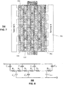
- the circular areas illustrated in FIG. 7 are vias 750 used to contact the top electrodes.
- the terminals A, B can communicate input and/or output signals to the individual capacitors formed by the top and bottom electrodes.
- the terminals A, B can have a comb shape with a terminal body 780 and a plurality of terminal fingers or connectors 785 extending therefrom, such as orthogonal from the terminal body. It should be understood that the examples useful for understanding can also include other numbers of groups of top electrodes subsections. Circuit 800 representative of capacitor 700 is illustrated in FIG. 8 showing the configuration of the series and parallel connections of the individual capacitors formed through use of the first and second groups of top electrodes with the bottom electrode.
- Capacitor 900 can reduce the series resistance of the bottom electrode by increasing the periphery length around each top or upper electrode.
- One means of increasing this periphery is use a nested array of crosses for the two top electrodes (e.g., a first group of cross-shaped electrodes 925 connected to terminal A and a second group of cross-shaped electrodes 925' connected to terminal B).
- the first and second groups of top electrodes are formed in an alternating pattern, but the exemplary embodiment can include other patterns being utilized to group the top electrodes.
- the bottom electrode can provide the connection between the capacitors formed by the first group of top electrodes and the capacitors formed by the second group of top electrodes.
- Capacitor 900 can provide for series and parallel connections of the individual capacitors formed through use of the first and second groups of top electrodes with the bottom electrode.
- the terminals A, B can communicate input and/or output signals to the individual capacitors formed by the top and bottom electrodes.
- the terminals A, B can have a terminal body 980 and a plurality of terminal fingers or connectors 985 extending therefrom.
- a portion of one or more of the terminal connectors 985 can be orthogonal to the terminal body 980.
- all or a portion of the terminal connectors 985 can be non-orthogonal to the terminal body 980 to facilitate connecting each of the first and second groups of top electrodes 925, 925' with terminals A, B, respectively.
- Capacitor 900 can utilize the cross-shaped top electrodes 925, 925' so as to maintain a consistent gap between each of the adjacent electrodes and/or maintain symmetry of the electrode subsection pattern.
- Other shapes can also be utilized for the crosses 925, 925' including other non-rectangular shapes.
- a combination of shapes can be utilized such as the crosses and half-crosses depicted in FIG. 9 .
- the non-rectangular shapes used for the top electrode subsections can provide for an electrode subsections having at least one edge that is parallel with another edge of an adjacent top electrode subsection.
- Capacitor 1000 can increase the zero bias Q.
- Capacitor 1000 can reduce the series resistance of the bottom electrode by increasing the periphery length around each top or upper electrode.
- One means of increasing this periphery is to use a comb-shaped upper electrode pattern comprising a first comb-shaped electrode 1025 and a second-comb shaped electrode 1025'.
- the bottom electrode can provide the connection between the capacitors formed from the first and second comb-shaped top electrodes 1025, 1025'.
- the comb-shaped electrodes 1025, 1025' can include an electrode body 1080 and a plurality of electrode fingers or connectors 1085 extending therefrom, such as orthogonal from the electrode body.
- the terminals A, B can communicate input and/or output signals to the individual capacitors formed by the top and bottom electrodes.
- the terminals A, B can be connected with the electrodes 1025, 1025" along or in proximity to the corresponding electrode bodies 1080. It should be understood that the example useful for understanding can also include other numbers of groups of top electrodes subsections.
- capacitor 1000 can utilize the first and second comb-shaped electrodes 1025, 1025' including the orthogonal electrode fingers or connectors 1085 so as to maintain a consistent gap between each of the two top electrodes.
- Capacitor 1100 can include a first capacitor portion or structure 1105 and a second capacitor portion or structure 1110. In one example useful for understanding, the first and second capacitors portions can be symmetrical.
- First capacitor portion 1105 can include top electrodes 1125, middle electrodes 1135, bottom electrodes 1145, and biasing terminal 1155.
- a dielectric medium(s) 1165 e.g., a tunable dielectric such as a BST material
- Second capacitor portion 1110 can include top electrodes 1125', middle electrodes 1135', bottom electrodes 1145', and biasing terminal 1155'.
- a dielectric medium(s) e.g., a tunable dielectric such as a BST material
- BST material can be used to separate the top, middle and bottom electrodes 1125', 1135', 1145' of the second capacitor portion 111.
- Capacitor 1100 can increase the perimeter length of middle electrodes 1135, 1135' without increasing the area of the electrodes.
- the broken concentric ring-like structure of capacitor 1100 can be used to enable a graded value of capacitance where the outer rings are higher capacitance values and the inner rings have lower capacitance values. With the appropriate resistive bias network, this arrangement of capacitors can permit lower time constants compared to a uniform distribution of capacitor values.
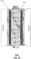
- Capacitor 1100 is illustrated as a dual layer capacitor, meaning that two capacitors are stacked vertically to make each ring. However, the examples useful for understanding can include single layer or multiple layers with more than two stacked layers that utilize all or a portion of the features of capacitor 1100.
- Cross section A-A illustrates the construction of the capacitors as stacked capacitors using three metal layers.
- each metal layer shown here may be a combination of metals.
- Pt may be used to contact the tunable dielectric layers (e.g., PARASCAN®) and/or TiW may be used next to the Pt for adhesion purposes.
- Other metals with higher electrical or thermal conductivity may be employed to lower the electrical and/or thermal resistance of each electrode.
- Capacitor 1100 can provide a symmetrical biasing network. Capacitor 1100 can achieve low charging times or low time constants for all capacitors in the string. Capacitor 1100 is in essence a splitting of the bias network into two halves, which may be symmetric as shown (or in one or more examples useful for understanding may be asymmetrical), to enable charging current to be injected equally along both sides of the capacitor string.
- the capacitor values can be graded in the following manner such that the largest capacitors are found near the ends of the string: C 1 ⁇ C 2 > C 3 ⁇ C 4 > C 5 ⁇ C 6 > C 7 ⁇ C 8 C 9 ⁇ C 10 ⁇ C 11 ⁇ C 12 ⁇ C 13 ⁇ C 14 ⁇ C 15 ⁇ C 16
- the bias resistors R m may be graded so as to have the largest resistor near the bias terminals: R m 1 > R m 2 > R m 3 > R m 4
- This bias resistor grading can also be done to facilitate equalizing the charging times across capacitors in the string.
- Circuit 1300 representative of capacitor 1100 is illustrated in FIG. 13 .
- any number of bias terminals can be utilized such as a single bias terminal or three or more bias terminals.
- the nested configuration can be adjusted based on the number of biasing terminals.
- any number of capacitor portions can be utilized, including using four portions with four bias terminals, where the four portions can share a center top electrode.
- One or more examples useful for understanding can utilize the nested ring capacitor configuration of FIG. 11 , but with different shapes for the electrodes.
- the four capacitor designs represent top electrode metal patterns built as nested rings.
- the examples useful for understanding can include other polygonal shapes which may or may not provide a symmetrical configuration.
- Bias resistors are omitted for clarity in FIGs. 14A-14D , but they can be located in the vicinity of the gaps in the outer rings.
- FIG. 15 is a block diagram of a system 1500 having a matching network 1510 that can utilize one or more of the exemplary capacitors or other components described herein.
- the matching network 1510 can be coupled to a tunable microwave device 1532.
- the tunable microwave device 1532 could be one of many devices which have varying input/output characteristic impedances such as tunable phase shifters, delay lines, filters, etc.
- the adjustable external DC voltage source 1534 can be used to supply bias voltage to the matching network 1510 and the tunable microwave device 1532 in tandem. As the voltage supplied by the external DC voltage source 1534 changes, the characteristic input/output impedance of the tunable dielectric device may also change.
- the impedance characteristics of the matching network 1510 can change to maximize, improve or otherwise adjust power transfer from/to the microwave source/load 1536 to/from the tunable microwave device 1532.
- the tunable microwave device 1532 and the matching network 1510 can be controlled by two different external DC voltage sources.
- the examples useful for understanding can be utilized in other circuits that may or may not include matching networks.
- an electrode can be broken into subsections with signal bus lines connecting the subsections and a solid electrode to improve Q.
- the method may further comprise distributing the signal across the capacitor area by the broken electrode and thereby increasing the effective width of a signal path through the solid electrode.
- the capacitor may be of various forms including a planar integrated capacitor or a discrete ceramic capacitor.
- the method may still further comprise adapting the solid electrode and the broken electrode to reduce the mechanical stresses generated in the metals and dielectric films of the capacitor.
- the capacitor can be utilized in a pair of series capacitors where the subsections are arranged in such a manner that it increases the effective width of the signal path in the solid electrode.
- a series network of voltage tunable dielectric capacitors can be provided, such as according to the steps and structures described herein, which are all, or a portion thereof, tuned using a common tuning voltage.
- a capacitor electrode structure allows for the creation of very high "Q" (e.g., low resistance) capacitors.
- one electrode can be made from a higher resistance metal than the opposite electrode, such as in planar integrated capacitors, as well as discrete ceramic capacitors.
- the electrodes can be broken into subsections, with signal bus lines connected to the subsections and/or to a solid electrode.
- the broken electrode preferably has the lower resistance material of the two.
- the broken electrode may distribute the signal across the capacitor area and, through proper arrangement, increase the effective width of the signal path through the higher resistance solid electrode.
- the signal busses may bring in and take out the signal. Voltage tunable dielectric material can be utilized between the electrodes.
- One or more of the examples or embodiments can include a first or bottom electrode(s), such as platinum, patterned and deposited into a substrate.
- a dielectric material, such as a thin film coating of a BST type material can be deposited on top of the bottom electrode, such as according to one or more of the exemplary configurations described above.
- a top or second electrode(s) can be deposited on top of the BST film.
- Interconnects, vias and the like can be utilized with the examples or the embodiments, including being deposited over a portion of the thin film structure, to provide attachment to other components, such as a microwave circuit and/or to provide an electrical path to at least one of the electrodes.
- Various materials including gold, aluminum and silver can be provided using various techniques including sputter and depositing to form some of the components of one or more of the examples or the embodiments, such as the electrode(s), the bus and so forth.
- a polymer encapsulation can be deposited to provide protection from ambient conditions and/or as a humidity barrier.
- multiple layers of dielectric materials (e.g., BST thin films) and/or electrodes can be deposited or otherwise formed to create an elaborate 3D structure of a multiple layer capacitor stack.
- One or more of the examples or the embodiments of the capacitor configurations can be utilized in various systems.
- wireless communications is a rapidly growing segment of the communications industry, with the potential to provide high-speed high-quality information exchange between portable devices located anywhere in the world.
- Potential applications enabled by one or more of the examples or the embodiments include multimedia internet-enabled cell phones, smart homes, appliances, automated highway systems, distance learning, and autonomous sensor networks, just to name a few.
- One or more of the examples or the embodiments can be used to enable low loss devices that can be used at higher frequency ranges.
- One or more of the examples or the embodiments can utilize relatively low capacitance varactors that can operate at temperatures above those necessary for superconduction and at bias voltages less than those required for existing planar varactor structures, while maintaining high tunability and high Q factors. Even though these materials may work in their paraelectric phase above the Curie temperature, they are conveniently called "ferroelectric” because they exhibit spontaneous polarization at temperatures below the Curie temperature.
- Tunable ferroelectric materials including barium-strontium titanate Ba x Sr 1-x TiO 3 (BST) or BST composites have been the subject of several patents.
- Dielectric materials including BST are disclosed by Sengupta, et al. in U.S. Pat. No. 5,312,790 ; U.S. Pat. No. 5,427,988 ; U.S. Pat. No. 5,486,491 ; U.S. Pat. No. 5,846,893 ; U.S. Pat. No. 5,635,434 ; U.S. Pat. No. 5,830,591 ; U.S. Pat. No. 5,766,697 ; U.S. Pat. No. 5,693,429 ; U.S. Pat. No. 6,074,971 ; U.S. Pat. No. 6,801,104 B2 and U.S. Pat. No. 5,635,433 .
- the dielectric constant of these materials can be varied by varying the strength of an electric field to which the materials are subjected. These materials allow for thin-film ferroelectric composites of low overall dielectric constant that takes advantage of the high tunability and at the same time having high dielectric constants. BST thin films can be used with one or more of the examples or the embodiments due to their high dielectric constant, high tunability, low loss, and fast switching speed.
- One or more of the examples or the embodiments can include the use of non-tunable dielectric material alone or in combination with other capacitors that utilize tunable dielectric material.
- the configuration of tunable and non-tunable capacitors formed by the examples or the embodiments can vary.
- the examples or the embodiments can also include the use of different dielectric materials by different individual capacitors formed by the segmented electrodes and the solid electrode, including a plurality of different tunable dielectric materials and/or a plurality of non-tunable dielectric materials forming individual capacitors that are in parallel and/or series and with each other.
- Quality factor, resonance frequency and breakdown voltage can be important factors for determining when thin film capacitor can be utilized.
- High-frequency device losses consist of material-related losses in the film and at the electrode-film interface, as well as the resistive losses in the electrodes.
- Thermal strain can occur on the interface between the ferroelectric thin film and the metal electrode due to the creation of oxide films and crystalline microstructure. This interface is generally the cause of losses at high frequencies and premature breakdown at low voltages.
- the designs on current devices are limited by traditional design guidelines that create resistive losses due to design constraints.
Landscapes
- Engineering & Computer Science (AREA)
- Power Engineering (AREA)
- Microelectronics & Electronic Packaging (AREA)
- Manufacturing & Machinery (AREA)
- Fixed Capacitors And Capacitor Manufacturing Machines (AREA)
- Ceramic Capacitors (AREA)
- Parts Printed On Printed Circuit Boards (AREA)
Claims (9)
- Segmentierter Kondensator (900), umfassend:eine erste Festelektrode (204);eine in Unterabschnitte (925, 925') aufgetrennte zweite Elektrode (201); undein dielektrisches Medium (203), das die Unterabschnitte (925, 925') von der ersten Festelektrode (204) trennt,wobei die Unterabschnitte (925, 925') der zweiten Elektrode (201) eine erste Gruppe von Unterabschnitten (925) und eine zweite Gruppe von Unterabschnitten (925') umfassen,wobei die erste Gruppe von Unterabschnitten (925) mit einem ersten Anschluss (A) zum Empfangen eines Eingangssignals verbindbar ist undwobei die zweite Gruppe von Unterabschnitten (925') mit einem zweiten Anschluss (B) zum Bereitstellen eines Ausgangssignals verbindbar ist,dadurch gekennzeichnet, dass die erste Gruppe von Unterabschnitten (925) und die zweite Gruppe von Unterabschnitten (925') ein vernestetes Array von Kreuzen bilden.
- Segmentierter Kondensator (900), wobei die erste Gruppe von Unterabschnitten (925) und die erste Festelektrode (204) eine erste Gruppe von Kondensatoren bilden,wobei die zweite Gruppe von Unterabschnitten (925') und die erste Festelektrode (204) eine zweite Gruppe von Kondensatoren bilden,wobei jeder Kondensator der ersten Gruppe von Kondensatoren elektrisch parallel geschaltet ist,wobei jeder Kondensator der zweiten Gruppe von Kondensatoren elektrisch parallel geschaltet ist undwobei die erste Gruppe von Kondensatoren mit der zweiten Gruppe von Kondensatoren elektrisch in Reihe geschaltet ist.
- Segmentierter Kondensator (900) nach einem der vorhergehenden Ansprüche, wobei der erste und zweite Anschluss (A, B) eine Kammform mit einem Anschlusskörper (980) und sich von dem Anschlusskörper (980) erstreckenden Anschlussverbindern (985) aufweisen und wobei der Anschlussverbinder (985) des ersten Anschlusses (A) und der Anschlussverbinder (985) des zweiten Anschlusses (B) unter Verwendung von Metalldurchkontaktierungen (950) mit der ersten Gruppe von Unterabschnitten (925) bzw. der zweiten Gruppe von Unterabschnitten (925') der zweiten Elektrode (201) verbunden sind.
- Segmentierter Kondensator (900) nach Anspruch 3, wobei mindestens ein Teil der Anschlussverbinder (985) zu dem Anschlusskörper (980) nicht orthogonal ist.
- Segmentierter Kondensator (900) nach einem der vorhergehenden Ansprüche, wobei die in die Unterabschnitte (925, 925') aufgetrennte zweite Elektrode (201) einen niedrigeren Widerstand als die erste Festelektrode (204) aufweist.
- Segmentierter Kondensator (900) nach einem der vorhergehenden Ansprüche, wobei die erste Gruppe von Unterabschnitten (925) und die erste Festelektrode (204) eine erste Gruppe von Kondensatoren bilden, wobei die zweite Gruppe von Unterabschnitten (925') und die erste Festelektrode (204) eine zweite Gruppe von Kondensatoren bilden und wobei die erste und zweite Gruppe von Kondensatoren in einem alternierenden Muster gebildet sind.
- Segmentierter Kondensator (900) nach einem der vorhergehenden Ansprüche, wobei der erste und zweite Anschluss (A, B) eine Kammform mit einem Anschlusskörper (980) und sich von dem Anschlusskörper (980) erstreckenden Anschlussverbindern (985) aufweisen.
- Segmentierter Kondensator (900) nach einem der vorhergehenden Ansprüche, wobei das dielektrische Medium ein abstimmbares dielektrisches Medium ist, das Barium-Strontium-Titanat umfasst.
- Segmentierter Kondensator (900) nach einem der vorhergehenden Ansprüche, wobei jeder angrenzende Unterabschnitt (925, 925') durch eine gleiche Lücke getrennt wird.
Applications Claiming Priority (1)
| Application Number | Priority Date | Filing Date | Title |
|---|---|---|---|
| US13/289,194 US9406444B2 (en) | 2005-11-14 | 2011-11-04 | Thin film capacitors |
Publications (3)
| Publication Number | Publication Date |
|---|---|
| EP2590190A2 EP2590190A2 (de) | 2013-05-08 |
| EP2590190A3 EP2590190A3 (de) | 2015-12-09 |
| EP2590190B1 true EP2590190B1 (de) | 2021-10-20 |
Family
ID=47177788
Family Applications (1)
| Application Number | Title | Priority Date | Filing Date |
|---|---|---|---|
| EP12191338.8A Not-in-force EP2590190B1 (de) | 2011-11-04 | 2012-11-05 | Dünnfilmkondensatoren |
Country Status (2)
| Country | Link |
|---|---|
| EP (1) | EP2590190B1 (de) |
| CA (1) | CA2794262C (de) |
Families Citing this family (3)
| Publication number | Priority date | Publication date | Assignee | Title |
|---|---|---|---|---|
| US9520904B2 (en) | 2013-11-13 | 2016-12-13 | Blackberry Limited | Apparatus and method for high linearity tuning |
| WO2022250640A1 (en) * | 2021-05-26 | 2022-12-01 | Ankara Yildirim Beyazit Universitesi | A novel wireless capacitive power transfer system |
| CN114203442B (zh) * | 2021-12-03 | 2023-11-03 | 灿芯半导体(上海)股份有限公司 | 一种用于高精度电容阵列的电容单元 |
Family Cites Families (10)
| Publication number | Priority date | Publication date | Assignee | Title |
|---|---|---|---|---|
| US5312790A (en) | 1993-06-09 | 1994-05-17 | The United States Of America As Represented By The Secretary Of The Army | Ceramic ferroelectric material |
| US5693429A (en) | 1995-01-20 | 1997-12-02 | The United States Of America As Represented By The Secretary Of The Army | Electronically graded multilayer ferroelectric composites |
| US5635433A (en) | 1995-09-11 | 1997-06-03 | The United States Of America As Represented By The Secretary Of The Army | Ceramic ferroelectric composite material-BSTO-ZnO |
| US5635434A (en) | 1995-09-11 | 1997-06-03 | The United States Of America As Represented By The Secretary Of The Army | Ceramic ferroelectric composite material-BSTO-magnesium based compound |
| US5846893A (en) | 1995-12-08 | 1998-12-08 | Sengupta; Somnath | Thin film ferroelectric composites and method of making |
| US5766697A (en) | 1995-12-08 | 1998-06-16 | The United States Of America As Represented By The Secretary Of The Army | Method of making ferrolectric thin film composites |
| US5830591A (en) | 1996-04-29 | 1998-11-03 | Sengupta; Louise | Multilayered ferroelectric composite waveguides |
| US6074971A (en) | 1998-11-13 | 2000-06-13 | The United States Of America As Represented By The Secretary Of The Army | Ceramic ferroelectric composite materials with enhanced electronic properties BSTO-Mg based compound-rare earth oxide |
| US6801104B2 (en) | 2000-08-22 | 2004-10-05 | Paratek Microwave, Inc. | Electronically tunable combline filters tuned by tunable dielectric capacitors |
| US7869186B2 (en) * | 2005-11-14 | 2011-01-11 | Paratek Microwave, Inc. | High Q and low stress capacitor electrode array |
-
2012
- 2012-11-05 CA CA2794262A patent/CA2794262C/en not_active Expired - Fee Related
- 2012-11-05 EP EP12191338.8A patent/EP2590190B1/de not_active Not-in-force
Non-Patent Citations (1)
| Title |
|---|
| None * |
Also Published As
| Publication number | Publication date |
|---|---|
| EP2590190A2 (de) | 2013-05-08 |
| CA2794262C (en) | 2016-12-13 |
| EP2590190A3 (de) | 2015-12-09 |
| CA2794262A1 (en) | 2013-05-04 |
Similar Documents
| Publication | Publication Date | Title |
|---|---|---|
| US10163574B2 (en) | Thin films capacitors | |
| Yoon et al. | A reduced intermodulation distortion tunable ferroelectric capacitor-architecture and demonstration | |
| US8130031B2 (en) | Tunable metamaterial | |
| USRE44998E1 (en) | Optimized thin film capacitors | |
| US8174341B2 (en) | Thin film based split resonator tunable metamaterial | |
| TW441146B (en) | Tunable microwave devices | |
| TW200901549A (en) | Variable filter element, variable filter module and fabrication method thereof | |
| Ji et al. | Ku-band antenna array feed distribution network with ferroelectric phase shifters on silicon | |
| EP2754189B1 (de) | Interdigitalkondensator mit fingern unterschiedlicher breite | |
| TWI754973B (zh) | 電容器結構 | |
| US12586744B2 (en) | Phase change material switch device and related methods | |
| EP2590190B1 (de) | Dünnfilmkondensatoren | |
| CN110959188A (zh) | 电容器 | |
| US10491159B2 (en) | Self-tuning microelectromechanical impedance matching circuits and methods of fabrication | |
| US9000866B2 (en) | Varactor shunt switches with parallel capacitor architecture | |
| KR20150014287A (ko) | 압전 시트, 이를 포함하는 압전 소자 및 압전 소자의 제조 방법 | |
| AU2002305531B2 (en) | Capacitor having improved electrodes | |
| EP2697861B1 (de) | Breitbandiger mikrowellen-hybridkoppler mit beliebiger phasenverschiebung und geteilter leistung | |
| US9424994B2 (en) | Tunable interdigitated capacitor | |
| US20060125052A1 (en) | Lateral tunable capacitor and high frequency tunable device having the same | |
| WO2022183764A1 (zh) | 带阻滤波器及其制作方法 | |
| US20240431220A1 (en) | Electronic device copmprising a layer of 2d material | |
| Poplavko et al. | MEMS-like phase shifter with piezoelectric control | |
| CN120239932A (zh) | 一种漏波天线及电子设备 | |
| US20140347781A1 (en) | Capacitor, Mems Device, and Method of Manufacturing the Mems Device |
Legal Events
| Date | Code | Title | Description |
|---|---|---|---|
| PUAI | Public reference made under article 153(3) epc to a published international application that has entered the european phase |
Free format text: ORIGINAL CODE: 0009012 |
|
| 17P | Request for examination filed |
Effective date: 20121105 |
|
| AK | Designated contracting states |
Kind code of ref document: A2 Designated state(s): AL AT BE BG CH CY CZ DE DK EE ES FI FR GB GR HR HU IE IS IT LI LT LU LV MC MK MT NL NO PL PT RO RS SE SI SK SM TR |
|
| AX | Request for extension of the european patent |
Extension state: BA ME |
|
| RAP1 | Party data changed (applicant data changed or rights of an application transferred) |
Owner name: BLACKBERRY LIMITED |
|
| RAP1 | Party data changed (applicant data changed or rights of an application transferred) |
Owner name: BLACKBERRY LIMITED |
|
| PUAL | Search report despatched |
Free format text: ORIGINAL CODE: 0009013 |
|
| AK | Designated contracting states |
Kind code of ref document: A3 Designated state(s): AL AT BE BG CH CY CZ DE DK EE ES FI FR GB GR HR HU IE IS IT LI LT LU LV MC MK MT NL NO PL PT RO RS SE SI SK SM TR |
|
| AX | Request for extension of the european patent |
Extension state: BA ME |
|
| RIC1 | Information provided on ipc code assigned before grant |
Ipc: H01G 4/33 20060101ALI20151102BHEP Ipc: H01G 4/012 20060101AFI20151102BHEP Ipc: H01G 4/38 20060101ALI20151102BHEP Ipc: H01G 7/06 20060101ALI20151102BHEP |
|
| STAA | Information on the status of an ep patent application or granted ep patent |
Free format text: STATUS: EXAMINATION IS IN PROGRESS |
|
| 17Q | First examination report despatched |
Effective date: 20190415 |
|
| RAP1 | Party data changed (applicant data changed or rights of an application transferred) |
Owner name: NXP USA, INC. |
|
| RIC1 | Information provided on ipc code assigned before grant |
Ipc: H01L 23/522 20060101ALN20210422BHEP Ipc: H01G 7/06 20060101ALI20210422BHEP Ipc: H01G 4/38 20060101ALI20210422BHEP Ipc: H01G 4/33 20060101ALI20210422BHEP Ipc: H01G 4/012 20060101AFI20210422BHEP |
|
| GRAP | Despatch of communication of intention to grant a patent |
Free format text: ORIGINAL CODE: EPIDOSNIGR1 |
|
| STAA | Information on the status of an ep patent application or granted ep patent |
Free format text: STATUS: GRANT OF PATENT IS INTENDED |
|
| RIC1 | Information provided on ipc code assigned before grant |
Ipc: H01L 23/522 20060101ALN20210518BHEP Ipc: H01G 7/06 20060101ALI20210518BHEP Ipc: H01G 4/38 20060101ALI20210518BHEP Ipc: H01G 4/33 20060101ALI20210518BHEP Ipc: H01G 4/012 20060101AFI20210518BHEP |
|
| INTG | Intention to grant announced |
Effective date: 20210609 |
|
| GRAS | Grant fee paid |
Free format text: ORIGINAL CODE: EPIDOSNIGR3 |
|
| GRAA | (expected) grant |
Free format text: ORIGINAL CODE: 0009210 |
|
| STAA | Information on the status of an ep patent application or granted ep patent |
Free format text: STATUS: THE PATENT HAS BEEN GRANTED |
|
| AK | Designated contracting states |
Kind code of ref document: B1 Designated state(s): AL AT BE BG CH CY CZ DE DK EE ES FI FR GB GR HR HU IE IS IT LI LT LU LV MC MK MT NL NO PL PT RO RS SE SI SK SM TR |
|
| REG | Reference to a national code |
Ref country code: GB Ref legal event code: FG4D |
|
| REG | Reference to a national code |
Ref country code: CH Ref legal event code: EP |
|
| REG | Reference to a national code |
Ref country code: DE Ref legal event code: R096 Ref document number: 602012076943 Country of ref document: DE |
|
| REG | Reference to a national code |
Ref country code: IE Ref legal event code: FG4D |
|
| REG | Reference to a national code |
Ref country code: AT Ref legal event code: REF Ref document number: 1440615 Country of ref document: AT Kind code of ref document: T Effective date: 20211115 |
|
| PGFP | Annual fee paid to national office [announced via postgrant information from national office to epo] |
Ref country code: FR Payment date: 20211117 Year of fee payment: 10 |
|
| REG | Reference to a national code |
Ref country code: LT Ref legal event code: MG9D |
|
| REG | Reference to a national code |
Ref country code: NL Ref legal event code: MP Effective date: 20211020 |
|
| REG | Reference to a national code |
Ref country code: AT Ref legal event code: MK05 Ref document number: 1440615 Country of ref document: AT Kind code of ref document: T Effective date: 20211020 |
|
| PG25 | Lapsed in a contracting state [announced via postgrant information from national office to epo] |
Ref country code: RS Free format text: LAPSE BECAUSE OF FAILURE TO SUBMIT A TRANSLATION OF THE DESCRIPTION OR TO PAY THE FEE WITHIN THE PRESCRIBED TIME-LIMIT Effective date: 20211020 Ref country code: LT Free format text: LAPSE BECAUSE OF FAILURE TO SUBMIT A TRANSLATION OF THE DESCRIPTION OR TO PAY THE FEE WITHIN THE PRESCRIBED TIME-LIMIT Effective date: 20211020 Ref country code: FI Free format text: LAPSE BECAUSE OF FAILURE TO SUBMIT A TRANSLATION OF THE DESCRIPTION OR TO PAY THE FEE WITHIN THE PRESCRIBED TIME-LIMIT Effective date: 20211020 Ref country code: BG Free format text: LAPSE BECAUSE OF FAILURE TO SUBMIT A TRANSLATION OF THE DESCRIPTION OR TO PAY THE FEE WITHIN THE PRESCRIBED TIME-LIMIT Effective date: 20220120 Ref country code: AT Free format text: LAPSE BECAUSE OF FAILURE TO SUBMIT A TRANSLATION OF THE DESCRIPTION OR TO PAY THE FEE WITHIN THE PRESCRIBED TIME-LIMIT Effective date: 20211020 |
|
| PG25 | Lapsed in a contracting state [announced via postgrant information from national office to epo] |
Ref country code: IS Free format text: LAPSE BECAUSE OF FAILURE TO SUBMIT A TRANSLATION OF THE DESCRIPTION OR TO PAY THE FEE WITHIN THE PRESCRIBED TIME-LIMIT Effective date: 20220220 Ref country code: SE Free format text: LAPSE BECAUSE OF FAILURE TO SUBMIT A TRANSLATION OF THE DESCRIPTION OR TO PAY THE FEE WITHIN THE PRESCRIBED TIME-LIMIT Effective date: 20211020 Ref country code: PT Free format text: LAPSE BECAUSE OF FAILURE TO SUBMIT A TRANSLATION OF THE DESCRIPTION OR TO PAY THE FEE WITHIN THE PRESCRIBED TIME-LIMIT Effective date: 20220221 Ref country code: PL Free format text: LAPSE BECAUSE OF FAILURE TO SUBMIT A TRANSLATION OF THE DESCRIPTION OR TO PAY THE FEE WITHIN THE PRESCRIBED TIME-LIMIT Effective date: 20211020 Ref country code: NO Free format text: LAPSE BECAUSE OF FAILURE TO SUBMIT A TRANSLATION OF THE DESCRIPTION OR TO PAY THE FEE WITHIN THE PRESCRIBED TIME-LIMIT Effective date: 20220120 Ref country code: NL Free format text: LAPSE BECAUSE OF FAILURE TO SUBMIT A TRANSLATION OF THE DESCRIPTION OR TO PAY THE FEE WITHIN THE PRESCRIBED TIME-LIMIT Effective date: 20211020 Ref country code: LV Free format text: LAPSE BECAUSE OF FAILURE TO SUBMIT A TRANSLATION OF THE DESCRIPTION OR TO PAY THE FEE WITHIN THE PRESCRIBED TIME-LIMIT Effective date: 20211020 Ref country code: HR Free format text: LAPSE BECAUSE OF FAILURE TO SUBMIT A TRANSLATION OF THE DESCRIPTION OR TO PAY THE FEE WITHIN THE PRESCRIBED TIME-LIMIT Effective date: 20211020 Ref country code: GR Free format text: LAPSE BECAUSE OF FAILURE TO SUBMIT A TRANSLATION OF THE DESCRIPTION OR TO PAY THE FEE WITHIN THE PRESCRIBED TIME-LIMIT Effective date: 20220121 Ref country code: ES Free format text: LAPSE BECAUSE OF FAILURE TO SUBMIT A TRANSLATION OF THE DESCRIPTION OR TO PAY THE FEE WITHIN THE PRESCRIBED TIME-LIMIT Effective date: 20211020 |
|
| REG | Reference to a national code |
Ref country code: CH Ref legal event code: PL |
|
| REG | Reference to a national code |
Ref country code: DE Ref legal event code: R097 Ref document number: 602012076943 Country of ref document: DE |
|
| PG25 | Lapsed in a contracting state [announced via postgrant information from national office to epo] |
Ref country code: SM Free format text: LAPSE BECAUSE OF FAILURE TO SUBMIT A TRANSLATION OF THE DESCRIPTION OR TO PAY THE FEE WITHIN THE PRESCRIBED TIME-LIMIT Effective date: 20211020 Ref country code: SK Free format text: LAPSE BECAUSE OF FAILURE TO SUBMIT A TRANSLATION OF THE DESCRIPTION OR TO PAY THE FEE WITHIN THE PRESCRIBED TIME-LIMIT Effective date: 20211020 Ref country code: RO Free format text: LAPSE BECAUSE OF FAILURE TO SUBMIT A TRANSLATION OF THE DESCRIPTION OR TO PAY THE FEE WITHIN THE PRESCRIBED TIME-LIMIT Effective date: 20211020 Ref country code: MC Free format text: LAPSE BECAUSE OF FAILURE TO SUBMIT A TRANSLATION OF THE DESCRIPTION OR TO PAY THE FEE WITHIN THE PRESCRIBED TIME-LIMIT Effective date: 20211020 Ref country code: LU Free format text: LAPSE BECAUSE OF NON-PAYMENT OF DUE FEES Effective date: 20211105 Ref country code: EE Free format text: LAPSE BECAUSE OF FAILURE TO SUBMIT A TRANSLATION OF THE DESCRIPTION OR TO PAY THE FEE WITHIN THE PRESCRIBED TIME-LIMIT Effective date: 20211020 Ref country code: DK Free format text: LAPSE BECAUSE OF FAILURE TO SUBMIT A TRANSLATION OF THE DESCRIPTION OR TO PAY THE FEE WITHIN THE PRESCRIBED TIME-LIMIT Effective date: 20211020 Ref country code: CZ Free format text: LAPSE BECAUSE OF FAILURE TO SUBMIT A TRANSLATION OF THE DESCRIPTION OR TO PAY THE FEE WITHIN THE PRESCRIBED TIME-LIMIT Effective date: 20211020 Ref country code: BE Free format text: LAPSE BECAUSE OF NON-PAYMENT OF DUE FEES Effective date: 20211130 |
|
| REG | Reference to a national code |
Ref country code: BE Ref legal event code: MM Effective date: 20211130 |
|
| PLBE | No opposition filed within time limit |
Free format text: ORIGINAL CODE: 0009261 |
|
| STAA | Information on the status of an ep patent application or granted ep patent |
Free format text: STATUS: NO OPPOSITION FILED WITHIN TIME LIMIT |
|
| PG25 | Lapsed in a contracting state [announced via postgrant information from national office to epo] |
Ref country code: LI Free format text: LAPSE BECAUSE OF NON-PAYMENT OF DUE FEES Effective date: 20211130 Ref country code: CH Free format text: LAPSE BECAUSE OF NON-PAYMENT OF DUE FEES Effective date: 20211130 |
|
| 26N | No opposition filed |
Effective date: 20220721 |
|
| GBPC | Gb: european patent ceased through non-payment of renewal fee |
Effective date: 20220120 |
|
| PG25 | Lapsed in a contracting state [announced via postgrant information from national office to epo] |
Ref country code: IE Free format text: LAPSE BECAUSE OF NON-PAYMENT OF DUE FEES Effective date: 20211105 Ref country code: GB Free format text: LAPSE BECAUSE OF NON-PAYMENT OF DUE FEES Effective date: 20220120 Ref country code: AL Free format text: LAPSE BECAUSE OF FAILURE TO SUBMIT A TRANSLATION OF THE DESCRIPTION OR TO PAY THE FEE WITHIN THE PRESCRIBED TIME-LIMIT Effective date: 20211020 |
|
| PG25 | Lapsed in a contracting state [announced via postgrant information from national office to epo] |
Ref country code: SI Free format text: LAPSE BECAUSE OF FAILURE TO SUBMIT A TRANSLATION OF THE DESCRIPTION OR TO PAY THE FEE WITHIN THE PRESCRIBED TIME-LIMIT Effective date: 20211020 |
|
| PGFP | Annual fee paid to national office [announced via postgrant information from national office to epo] |
Ref country code: DE Payment date: 20221020 Year of fee payment: 11 |
|
| PG25 | Lapsed in a contracting state [announced via postgrant information from national office to epo] |
Ref country code: IT Free format text: LAPSE BECAUSE OF FAILURE TO SUBMIT A TRANSLATION OF THE DESCRIPTION OR TO PAY THE FEE WITHIN THE PRESCRIBED TIME-LIMIT Effective date: 20211020 Ref country code: HU Free format text: LAPSE BECAUSE OF FAILURE TO SUBMIT A TRANSLATION OF THE DESCRIPTION OR TO PAY THE FEE WITHIN THE PRESCRIBED TIME-LIMIT; INVALID AB INITIO Effective date: 20121105 Ref country code: CY Free format text: LAPSE BECAUSE OF FAILURE TO SUBMIT A TRANSLATION OF THE DESCRIPTION OR TO PAY THE FEE WITHIN THE PRESCRIBED TIME-LIMIT Effective date: 20211020 |
|
| P01 | Opt-out of the competence of the unified patent court (upc) registered |
Effective date: 20230725 |
|
| PG25 | Lapsed in a contracting state [announced via postgrant information from national office to epo] |
Ref country code: FR Free format text: LAPSE BECAUSE OF NON-PAYMENT OF DUE FEES Effective date: 20221130 |
|
| PG25 | Lapsed in a contracting state [announced via postgrant information from national office to epo] |
Ref country code: MK Free format text: LAPSE BECAUSE OF FAILURE TO SUBMIT A TRANSLATION OF THE DESCRIPTION OR TO PAY THE FEE WITHIN THE PRESCRIBED TIME-LIMIT Effective date: 20211020 |
|
| REG | Reference to a national code |
Ref country code: DE Ref legal event code: R119 Ref document number: 602012076943 Country of ref document: DE |
|
| PG25 | Lapsed in a contracting state [announced via postgrant information from national office to epo] |
Ref country code: MT Free format text: LAPSE BECAUSE OF FAILURE TO SUBMIT A TRANSLATION OF THE DESCRIPTION OR TO PAY THE FEE WITHIN THE PRESCRIBED TIME-LIMIT Effective date: 20211020 |
|
| PG25 | Lapsed in a contracting state [announced via postgrant information from national office to epo] |
Ref country code: DE Free format text: LAPSE BECAUSE OF NON-PAYMENT OF DUE FEES Effective date: 20240601 |
|
| PG25 | Lapsed in a contracting state [announced via postgrant information from national office to epo] |
Ref country code: DE Free format text: LAPSE BECAUSE OF NON-PAYMENT OF DUE FEES Effective date: 20240601 |
|
| PG25 | Lapsed in a contracting state [announced via postgrant information from national office to epo] |
Ref country code: TR Free format text: LAPSE BECAUSE OF FAILURE TO SUBMIT A TRANSLATION OF THE DESCRIPTION OR TO PAY THE FEE WITHIN THE PRESCRIBED TIME-LIMIT Effective date: 20211020 |