EP2070634A1 - Laser processing device - Google Patents
Laser processing device Download PDFInfo
- Publication number
- EP2070634A1 EP2070634A1 EP07807875A EP07807875A EP2070634A1 EP 2070634 A1 EP2070634 A1 EP 2070634A1 EP 07807875 A EP07807875 A EP 07807875A EP 07807875 A EP07807875 A EP 07807875A EP 2070634 A1 EP2070634 A1 EP 2070634A1
- Authority
- EP
- European Patent Office
- Prior art keywords
- laser light
- processing
- converging lens
- converging
- processing laser
- Prior art date
- Legal status (The legal status is an assumption and is not a legal conclusion. Google has not performed a legal analysis and makes no representation as to the accuracy of the status listed.)
- Granted
Links
Images




Classifications
-
- B—PERFORMING OPERATIONS; TRANSPORTING
- B23—MACHINE TOOLS; METAL-WORKING NOT OTHERWISE PROVIDED FOR
- B23K—SOLDERING OR UNSOLDERING; WELDING; CLADDING OR PLATING BY SOLDERING OR WELDING; CUTTING BY APPLYING HEAT LOCALLY, e.g. FLAME CUTTING; WORKING BY LASER BEAM
- B23K26/00—Working by laser beam, e.g. welding, cutting or boring
- B23K26/36—Removing material
- B23K26/38—Removing material by boring or cutting
-
- B—PERFORMING OPERATIONS; TRANSPORTING
- B23—MACHINE TOOLS; METAL-WORKING NOT OTHERWISE PROVIDED FOR
- B23K—SOLDERING OR UNSOLDERING; WELDING; CLADDING OR PLATING BY SOLDERING OR WELDING; CUTTING BY APPLYING HEAT LOCALLY, e.g. FLAME CUTTING; WORKING BY LASER BEAM
- B23K26/00—Working by laser beam, e.g. welding, cutting or boring
- B23K26/02—Positioning or observing the workpiece, e.g. with respect to the point of impact; Aligning, aiming or focusing the laser beam
- B23K26/04—Automatically aligning, aiming or focusing the laser beam, e.g. using the back-scattered light
- B23K26/046—Automatically focusing the laser beam
- B23K26/048—Automatically focusing the laser beam by controlling the distance between laser head and workpiece
-
- B—PERFORMING OPERATIONS; TRANSPORTING
- B23—MACHINE TOOLS; METAL-WORKING NOT OTHERWISE PROVIDED FOR
- B23K—SOLDERING OR UNSOLDERING; WELDING; CLADDING OR PLATING BY SOLDERING OR WELDING; CUTTING BY APPLYING HEAT LOCALLY, e.g. FLAME CUTTING; WORKING BY LASER BEAM
- B23K26/00—Working by laser beam, e.g. welding, cutting or boring
- B23K26/02—Positioning or observing the workpiece, e.g. with respect to the point of impact; Aligning, aiming or focusing the laser beam
- B23K26/06—Shaping the laser beam, e.g. by masks or multi-focusing
- B23K26/062—Shaping the laser beam, e.g. by masks or multi-focusing by direct control of the laser beam
- B23K26/0622—Shaping the laser beam, e.g. by masks or multi-focusing by direct control of the laser beam by shaping pulses
- B23K26/0624—Shaping the laser beam, e.g. by masks or multi-focusing by direct control of the laser beam by shaping pulses using ultrashort pulses, i.e. pulses of 1 ns or less
-
- B—PERFORMING OPERATIONS; TRANSPORTING
- B23—MACHINE TOOLS; METAL-WORKING NOT OTHERWISE PROVIDED FOR
- B23K—SOLDERING OR UNSOLDERING; WELDING; CLADDING OR PLATING BY SOLDERING OR WELDING; CUTTING BY APPLYING HEAT LOCALLY, e.g. FLAME CUTTING; WORKING BY LASER BEAM
- B23K26/00—Working by laser beam, e.g. welding, cutting or boring
- B23K26/02—Positioning or observing the workpiece, e.g. with respect to the point of impact; Aligning, aiming or focusing the laser beam
- B23K26/06—Shaping the laser beam, e.g. by masks or multi-focusing
- B23K26/064—Shaping the laser beam, e.g. by masks or multi-focusing by means of optical elements, e.g. lenses, mirrors or prisms
-
- B—PERFORMING OPERATIONS; TRANSPORTING
- B23—MACHINE TOOLS; METAL-WORKING NOT OTHERWISE PROVIDED FOR
- B23K—SOLDERING OR UNSOLDERING; WELDING; CLADDING OR PLATING BY SOLDERING OR WELDING; CUTTING BY APPLYING HEAT LOCALLY, e.g. FLAME CUTTING; WORKING BY LASER BEAM
- B23K26/00—Working by laser beam, e.g. welding, cutting or boring
- B23K26/02—Positioning or observing the workpiece, e.g. with respect to the point of impact; Aligning, aiming or focusing the laser beam
- B23K26/06—Shaping the laser beam, e.g. by masks or multi-focusing
- B23K26/067—Dividing the beam into multiple beams, e.g. multi-focusing
- B23K26/0676—Dividing the beam into multiple beams, e.g. multi-focusing into dependently operating sub-beams, e.g. an array of spots with fixed spatial relationship or for performing simultaneously identical operations
-
- B—PERFORMING OPERATIONS; TRANSPORTING
- B23—MACHINE TOOLS; METAL-WORKING NOT OTHERWISE PROVIDED FOR
- B23K—SOLDERING OR UNSOLDERING; WELDING; CLADDING OR PLATING BY SOLDERING OR WELDING; CUTTING BY APPLYING HEAT LOCALLY, e.g. FLAME CUTTING; WORKING BY LASER BEAM
- B23K26/00—Working by laser beam, e.g. welding, cutting or boring
- B23K26/08—Devices involving relative movement between laser beam and workpiece
- B23K26/083—Devices involving movement of the workpiece in at least one axial direction
- B23K26/0853—Devices involving movement of the workpiece in at least two axial directions, e.g. in a plane
-
- B—PERFORMING OPERATIONS; TRANSPORTING
- B23—MACHINE TOOLS; METAL-WORKING NOT OTHERWISE PROVIDED FOR
- B23K—SOLDERING OR UNSOLDERING; WELDING; CLADDING OR PLATING BY SOLDERING OR WELDING; CUTTING BY APPLYING HEAT LOCALLY, e.g. FLAME CUTTING; WORKING BY LASER BEAM
- B23K26/00—Working by laser beam, e.g. welding, cutting or boring
- B23K26/08—Devices involving relative movement between laser beam and workpiece
- B23K26/0869—Devices involving movement of the laser head in at least one axial direction
-
- B—PERFORMING OPERATIONS; TRANSPORTING
- B23—MACHINE TOOLS; METAL-WORKING NOT OTHERWISE PROVIDED FOR
- B23K—SOLDERING OR UNSOLDERING; WELDING; CLADDING OR PLATING BY SOLDERING OR WELDING; CUTTING BY APPLYING HEAT LOCALLY, e.g. FLAME CUTTING; WORKING BY LASER BEAM
- B23K26/00—Working by laser beam, e.g. welding, cutting or boring
- B23K26/36—Removing material
- B23K26/40—Removing material taking account of the properties of the material involved
-
- B—PERFORMING OPERATIONS; TRANSPORTING
- B23—MACHINE TOOLS; METAL-WORKING NOT OTHERWISE PROVIDED FOR
- B23K—SOLDERING OR UNSOLDERING; WELDING; CLADDING OR PLATING BY SOLDERING OR WELDING; CUTTING BY APPLYING HEAT LOCALLY, e.g. FLAME CUTTING; WORKING BY LASER BEAM
- B23K26/00—Working by laser beam, e.g. welding, cutting or boring
- B23K26/36—Removing material
- B23K26/40—Removing material taking account of the properties of the material involved
- B23K26/402—Removing material taking account of the properties of the material involved involving non-metallic material, e.g. isolators
-
- B—PERFORMING OPERATIONS; TRANSPORTING
- B23—MACHINE TOOLS; METAL-WORKING NOT OTHERWISE PROVIDED FOR
- B23K—SOLDERING OR UNSOLDERING; WELDING; CLADDING OR PLATING BY SOLDERING OR WELDING; CUTTING BY APPLYING HEAT LOCALLY, e.g. FLAME CUTTING; WORKING BY LASER BEAM
- B23K26/00—Working by laser beam, e.g. welding, cutting or boring
- B23K26/50—Working by transmitting the laser beam through or within the workpiece
- B23K26/53—Working by transmitting the laser beam through or within the workpiece for modifying or reforming the material inside the workpiece, e.g. for producing break initiation cracks
-
- H—ELECTRICITY
- H10—SEMICONDUCTOR DEVICES; ELECTRIC SOLID-STATE DEVICES NOT OTHERWISE PROVIDED FOR
- H10P—GENERIC PROCESSES OR APPARATUS FOR THE MANUFACTURE OR TREATMENT OF DEVICES COVERED BY CLASS H10
- H10P95/00—Generic processes or apparatus for manufacture or treatments not covered by the other groups of this subclass
-
- B—PERFORMING OPERATIONS; TRANSPORTING
- B23—MACHINE TOOLS; METAL-WORKING NOT OTHERWISE PROVIDED FOR
- B23K—SOLDERING OR UNSOLDERING; WELDING; CLADDING OR PLATING BY SOLDERING OR WELDING; CUTTING BY APPLYING HEAT LOCALLY, e.g. FLAME CUTTING; WORKING BY LASER BEAM
- B23K2101/00—Articles made by soldering, welding or cutting
- B23K2101/36—Electric or electronic devices
- B23K2101/40—Semiconductor devices
-
- B—PERFORMING OPERATIONS; TRANSPORTING
- B23—MACHINE TOOLS; METAL-WORKING NOT OTHERWISE PROVIDED FOR
- B23K—SOLDERING OR UNSOLDERING; WELDING; CLADDING OR PLATING BY SOLDERING OR WELDING; CUTTING BY APPLYING HEAT LOCALLY, e.g. FLAME CUTTING; WORKING BY LASER BEAM
- B23K2103/00—Materials to be soldered, welded or cut
- B23K2103/50—Inorganic materials other than metals or composite materials
Definitions
- the present invention relates to a laser processing apparatus for cutting a planar object to be processed along a line to cut.
- a conventional laser processing apparatus is one which irradiates a planar object to be processed with processing laser light while locating a converging point within the object, so as to form a modified region to become a cutting start point within the object along a line to cut the object (see, for example, Patent Literature 1).
- a laser processing apparatus such as the one mentioned above to cut a relatively thick object to be processed having a thickness of 100 ⁇ m or more, for example. That is, for forming a modified region accurately at a predetermined position distanced from a laser light irradiation surface of the object, it is necessary to emit (trace) measuring laser light for measuring a displacement of the laser light irradiation surface along the line to cut before forming the modified region by irradiation with the processing laser light. Further, for accurately cutting the object, a plurality of rows of modified regions are required to be formed in the thickness direction of the object, which makes it necessary to scan the processing laser light along the same line to cut a plurality of times according to the number of rows of modified regions. Therefore, it may take a long time for the laser processing apparatus such as the one mentioned above to form the modified regions within the object, thereby increasing the running cost.
- the laser processing apparatus in accordance with the present invention is a laser processing apparatus for irradiating a planar object to be processed with processing laser light while locating a converging point within the object, so as to form a modified region to become a cutting start point within the object along a line to cut the object, the apparatus comprising a mount table for mounting the object; a processing laser light source for emitting the processing laser light as linearly polarized light; a measuring laser light source for emitting measuring laser light for irradiating the object; a first half-wave plate for changing a polarization direction of the processing laser light emitted from the processing laser light source; a polarizing plate for splitting the processing laser light transmitted through the first half-wave plate into a processing laser light component having a polarization direction in a predetermined direction and a processing laser light component having a polarization direction in a direction intersecting the predetermined direction; a second half-wave plate for changing the polarization direction
- the laser processing apparatus in accordance with the present invention is a laser processing apparatus for irradiating a planar object to be processed with processing laser light while locating a converging point within the object, so as to form a modified region to become a cutting start point within the object along a line to cut the object
- the apparatus comprising a mount table for mounting the object; a processing laser light source for emitting the processing laser light as linearly polarized light; a measuring laser light source for emitting measuring laser light for irradiating the object; a first half-wave plate for changing a polarization direction of the processing laser light emitted from the processing laser light source; a polarizing plate for splitting the processing laser light transmitted through the first half-wave plate into a processing laser light component having a polarization direction in a predetermined direction and a processing laser light component having a polarization direction in a direction intersecting the predetermined direction; a second half-wave plate for changing the polarization direction of the processing laser light component, split by the polarization direction
- linearly polarized processing laser light is emitted from a processing laser light source, changes the polarization direction with a first half-wave plate, and then is incident on a polarizing plate.
- the polarizing plate splits the processing laser light into a processing light component having a polarization direction in a predetermined direction and a processing light component having a polarization direction in a direction intersecting the predetermined direction.
- the processing laser light component, split by the polarizing plate, having the polarization direction in the direction intersecting the predetermined direction changes the polarization direction to the predetermined direction because of a second half-wave plate.
- the linearly polarized processing laser light is split into respective components incident on the first and second converging lenses, while having the converging direction in the predetermined direction. Then, in this case, as at least one of the pair of first and second converging lenses and the mount table is relatively moved by the moving means along the line to cut in a state where the predetermined direction substantially coincides with the line to cut, for example, the measuring laser light is emitted from the measuring laser light source, and control means detects a reflected light component of the measuring laser light reflected by the laser light irradiation surface of the object, whereby the distance between the laser light irradiation surface and the second converging lens is regulated such that a converging point of the processing laser light converged by the second converging lens is located at a predetermined position with reference to the laser light irradiation surface.
- control means detects the reflected light component of the measuring laser light reflected by the laser light irradiation surface so as to regulate a distance between the laser light irradiation surface and the first converging lens such that a converging point of the processing laser light converged by the first converging lens is located at a predetermined position with reference to the laser light irradiation surface.
- the control means detects a reflected light component of the measuring laser light reflected by the laser light irradiation surface of the object, whereby the distance between the laser light irradiation surface and the first converging lens is regulated such that a converging point of the processing laser light converged by the first converging lens is located at a predetermined position with reference to the laser light irradiation surface, while the distance between the laser light irradiation surface and the second converging lens is regulated such that a converging point of the processing laser light converged by the second converging lens is located at a predetermined position with reference to the laser light irradiation surface.
- the first half-wave plate changes the polarization direction of the processing laser light to a given direction.
- portions of light quantities of the processing laser light components split by the polarizing plate can be adjusted arbitrarily according to the polarization direction of the processing laser light transmitted through the first half-wave plate.
- the apparatus further comprises an attenuator, arranged between the processing laser light source and the first half-wave plate in an optical path of the processing laser light, for adjusting a light quantity of the processing laser light.
- the attenuator can adjust the light quantity of the processing laser light incident on the first half-wave plate, so as to change the total output of the processing laser light freely.
- the apparatus further comprises a shutter, arranged between the polarizing plate and the first converging lens in an optical path of the processing laser light, for blocking the processing laser light from being made incident on the first converging lens.
- closing the shutter can reliably and easily inhibit the first converging lens from converging the processing laser light toward the object. This is effective in particular when only the displacement measurement for the laser light irradiation surface with the first converging lens is carried out by using the first converging lens.
- the control means executes control for operating the first converging lens such that the first converging lens is separated from the laser light irradiation surface by a constant distance and, while acquiring operation information concerning the operation, operating the second convergent lens according to the operation information and the predetermined distance, and control for operating the first converging lens according to the operation information acquired beforehand and operating the second converging lens according to the operation information acquired beforehand and the predetermined distance.
- the present invention makes it possible to provide a laser processing apparatus which can shorten the time required for forming a modified region within an object to be processed.
- a material becomes transparent when its absorption bandgap E G is greater than photon energy hv. Consequently, a condition under which absorption occurs in the material is hv > E G . However, even when optically transparent, the material generates absorption under a condition of nhv > E G (where n 2, 3, 4, ...) if the intensity of laser light becomes very high. This phenomenon is known as multiphoton absorption. In the case of pulsed waves, the intensity of laser light is determined by the peak power density (W/cm 2 ) of laser light at its converging point. The multiphoton absorption occurs under a condition where the peak power density is 1 ⁇ 10 8 (W/cm 2 ) or greater, for example.
- the peak power density is determined by (energy of laser light at the converging point per pulse)/(beam spot cross-sectional area of laser light ⁇ pulse width).
- the intensity of laser light is determined by the field intensity (W/cm 2 ) of laser light at the converging point.
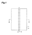
- a line to cut 5 for cutting the object 1 exists on a front face 3 of a wafer-like (planar) object to be processed 1.
- the line to cut 5 is a virtual line extending straight.
- the laser processing method in accordance with this embodiment irradiates the object 1 with laser light L while locating a converging point P therewithin under a condition generating multiphoton absorption, so as to form a modified region 7.
- the converging point P is a position at which the laser light L is converged.
- the line to cut 5 may be curved instead of being straight, and may be a line actually drawn on the object 1 without being restricted to the virtual line.
- the laser light L is relatively moved along the line to cut 5 (i.e., in the direction of arrow A in Fig. 1 ), so as to shift the converging point P along the line to cut 5. Consequently, as illustrated in Figs. 3 to 5 , the modified region 7 is formed along the line to cut 5 within the object 1, and becomes a cutting start region 8.
- the cutting start region 8 refers to a region which becomes a start point for cutting (fracturing) when the object 1 is cut.
- the cutting start region 8 may be made by forming the modified region 7 either continuously or intermittently.
- the front face 3 of the object 1 hardly absorbs the laser light L and thus does not melt.
- Forming the cutting start region 8 within the object 1 makes it easier to generate fractures from the cutting start region 8 acting as a start point, whereby the object 1 can be cut with a relatively small force as illustrated in Fig. 6 . Therefore, the object 1 can be cut with a high precision without generating unnecessary fractures on the front face 3 of the object 1.
- the other is where the forming of the cutting start region 8 causes the object 1 to fracture naturally in its cross-sectional direction (thickness direction) from the cutting start region 8 acting as a start point, thereby cutting the object 1.
- the modified region formed by multiphoton absorption in the laser processing method in accordance with this embodiment encompasses the following cases (1) to (3):
- the modified region is a crack region including one or a plurality of cracks
- An object to be processed e.g., glass or a piezoelectric material made of LiTaO 3
- This magnitude of pulse width is a condition under which a crack region can be formed only within the object while generating multiphoton absorption without causing unnecessary damages to the front face of the object. This generates a phenomenon of optical damage by multiphoton absorption within the object.
- This optical damage induces a thermal distortion within the object, thereby forming a crack region therewithin.
- the upper limit of field intensity is 1 ⁇ 10 12 (W/cm 2 ), for example.
- the pulse width is preferably 1 ns to 200 ns, for example.
- the inventors determined the relationship between field intensity and crack size by an experiment. The following are conditions of the experiment.
- the laser light quality of TEM 00 means that the converging characteristic is so high that convergence to about the wavelength of laser light is possible.
- Fig. 7 is a graph illustrating the results of the above-mentioned experiment.
- the abscissa indicates the peak power density. Since the laser light is pulsed laser light, the field intensity is represented by the peak power density.
- the ordinate indicates the size of a crack part (crack spot) formed within the object by one pulse of laser light. Crack spots gather to yield a crack region. The crack spot size is the size of a part yielding the maximum length among forms of crack spots.
- Data represented by black circles in the graph refer to a case where the converging lens (C) has a magnification of x 100 and a numerical aperture (NA) of 0.80.
- data represented by whitened circles in the graph refer to a case where the converging lens (C) has a magnification of x50 and a numerical aperture (NA) of 0.55. Crack spots are seen to occur within the object from when the peak power density is about 10 11 (W/cm 2 ) and become greater as the peak power density increases.
- FIG. 8 the object 1 is irradiated with laser light L while the converging point P is located within the object 1 under a condition where multiphoton absorption occurs, so as to form a crack region 9 therewithin along a line to cut.
- the crack region 9 is a region containing one or a plurality of cracks.
- formed crack region 9 becomes a cutting start region.
- a crack further grows from the crack region 9 acting as a start point (i.e., from the cutting start region acting as a start point) as illustrated in Fig.
- the modified region is a molten processed region
- An object to be processed e.g., semiconductor material such as silicon
- the inside of the object is locally heated by multiphoton absorption. This heating forms a molten processed region within the object.
- the molten processed region encompasses regions once molten and then re-solidified, regions just in a molten state, and regions in the process of being re-solidified from the molten state, and can also be referred to as a region whose phase has changed or a region whose crystal structure has changed.
- the molten processed region may also be referred to as a region in which a certain structure changes to another structure among monocrystal, amorphous, and polycrystal structures.
- the molten processed region is an amorphous silicon structure, for example.
- the upper limit of field intensity is 1 ⁇ 10 12 (W/cm 2 ), for example.
- the pulse width is preferably 1 ns to 200 ns, for example.
- the inventors verified that a molten processed region was formed within a silicon wafer (semiconductor substrate). The following are conditions of the experiment.
- Fig. 12 is a view illustrating a photograph of a cross section of a part of a silicon wafer cut by laser processing under the conditions mentioned above.
- a molten processed region 13 is formed within the silicon wafer 11.
- the molten processed region 13 formed under the above-mentioned conditions has a size of about 100 ⁇ m in the thickness direction.
- Fig. 13 is a graph illustrating relationships between the laser light wavelength and the transmittance within the silicon substrate.
- the respective reflected components on the front and rear sides of the silicon substrate are eliminated, so as to represent the internal transmittance alone.
- the respective relationships are illustrated in the cases where the thickness t of the silicon substrate is 50 ⁇ m, 100 ⁇ m, 200 ⁇ m, 500 ⁇ m, and 1000 ⁇ m.
- the laser light appears to be transmitted through the silicon substrate by at least 80% when the silicon substrate has a thickness of 500 ⁇ m or less.
- the silicon wafer 11 illustrated in Fig. 12 has a thickness of 350 ⁇ m, the molten processed region 13 caused by multiphoton absorption is formed near the center of the silicon wafer 11, i.e., at a part distanced from the front face by 175 ⁇ m.
- the transmittance in this case is 90% or more with reference to a silicon wafer having a thickness of 200 ⁇ m, whereby the laser light is absorbed only slightly within the silicon wafer 11 but is substantially transmitted therethrough.
- the molten processed region 13 is formed within the silicon wafer 11 not by the absorption of laser light within the silicon wafer 11 (i.e., not by usual heating with the laser light) but by multiphoton absorption.
- the forming of a molten processed region by multiphoton absorption is disclosed, for example, in " Ultrashort Pulse Laser Microprocessing of Silicon", Preprints of the National Meetings of Japan Welding Society, Vol. 66 (April, 2000), pp. 72-73 .
- a fracture is generated in a silicon wafer from a cutting start region formed by a molten processed region, acting as a start point, in a cross-sectional direction, and reaches the front and rear faces of the silicon wafer, whereby the silicon wafer is cut.
- the fracture reaching the front and rear faces of the silicon wafer may grow naturally or as a force is applied to the silicon wafer.
- the fracture naturally growing from the cutting start region to the front and rear faces of the silicon wafer encompasses a case where the fracture grows from a state in which the molten processed region forming the cutting start region is molten and a case where the fracture grows when the molten processed region forming the cutting start region is re-solidified from the molten state.
- the molten processed region is formed only within the silicon wafer, and thus is present only within the cut section after cutting as illustrated in Fig. 12 .
- a cutting start region is thus formed within the object by a molten processed region, unnecessary fractures deviating from a cutting start region line are harder to occur at the time of cleaving, whereby cleavage control becomes easier.
- the molten processed region may be formed not only by multiphoton absorption but also by other absorption actions.
- the modified region is a refractive index change region
- An object to be processed e.g., glass
- the energy caused by multiphoton absorption is not converted into thermal energy, whereby an eternal structure change such as ion valence change, crystallization, or orientation polarization is induced within the object, thus forming a refractive index change region.
- the upper limit of field intensity is 1 ⁇ 10 12 (W/cm 2 ), for example.
- the pulse width is preferably 1 ns or less, for example, more preferably 1 ps or less.
- a cutting start region may be formed as follows while taking account of the crystal structure of a wafer-like object to be processed, its cleavage characteristic, and the like, whereby the object can be cut with a favorable precision by a smaller force from the cutting start region acting as a start point.
- a cutting start region is formed in a direction extending along a (111) plane (first cleavage plane) or a (110) plane (second cleavage plane).
- a substrate made of a group III-V compound semiconductor of sphalerite structure such as GaAs
- a cutting start region is formed in a direction extending along a (1120) plane (A plane) or a (1100) plane (M plane) while using a (0001) plane (C plane) as a principal plane.
- the cutting start region extending in the direction to be formed with the cutting start region can be formed easily and accurately with reference to the orientation flat.
- an object to be processed 1 comprises a silicon wafer 11 having a thickness of 300 ⁇ m and a diameter of 8 inches and a functional device layer 16 which is formed on a front face 11a of the silicon wafer 11 while including a plurality of functional devices 15.
- a number of functional devices 15, examples of which include semiconductor operating layers formed by crystal growth, light-receiving devices such as photodiodes, light-emitting devices such as laser diodes, and circuit devices formed as circuits, are formed like a matrix in directions parallel and perpendicular to an orientation flat 6 of the silicon wafer 11.
- Such an object to be processed 1 is cut along lines to cut 5 which are set like grids passing between the functional devices adjacent to each other, so as to become chips each having a size of 1 mm ⁇ 1 mm, for example.
- a laser processing apparatus 100 irradiates the planar object to be processed 1 with laser light (processing laser light) L while locating a converging point within the object 1, so as to form a plurality of rows of modified regions to become a cutting start point within the object 1 along the lines 5 to cut the object 1.
- laser light processing laser light
- the laser processing apparatus 100 comprises a mount table 107 for mounting the object 1 horizontally, a laser unit 110, and a movement control section (moving means) 115 for moving the mount table 107 and laser unit 110.
- the movement control section 115 moves the mount table 107 in horizontal directions (X and Y directions) and the laser unit 110 in vertical directions (Z directions).
- the laser unit 110 is equipped with a processing laser light source 101 for pulse-oscillating linearly polarized processing laser light L having a polarization direction in the X direction (predetermined direction).
- the processing laser light L emitted from the processing laser light source 101 passes through an attenuator 102 for adjusting the light quantity of the processing laser light L, so as to be guided to a separator 103 for splitting it into a linearly polarized processing laser light component L1 having a polarization direction in the X direction and a linearly polarized processing laser light component L2 having a polarization direction in the Y direction (direction intersecting the predetermined direction).
- the split processing laser light component L1 is successively guided to a shutter 33 for transmitting or blocking the processing laser light component L1, a beam expander 35 for expanding its beam size, and a dichroic mirror 48, and then is converged by a converging lens (first converging lens) 31, so as to irradiate the object 1.
- the converging lens 31 is one which converges the processing laser light component L 1 and measuring laser light L3, which will be explained later, toward the object 1.
- a piezoelectric device 28 is attached to the converging lens 31, so as to adjust the Z-directional position of the converging lens 31.
- the dichroic mirror 48 transmits the processing laser light component L1 therethrough but reflects the measuring laser light L3 and its reflected light component L4, which will be explained later.
- the split processing laser light component L2 is successively guided to a mirror 22, a shutter 34, and a beam expander 36, so as to be turned into linearly polarized light having a polarization direction in the X direction by an attenuator 104, and then is converged by a converging lens (second converging lens) 32, so as to irradiate the object 1.
- the converging lens 32 which is arranged in parallel with the converging lens 31 while being separated therefrom by a predetermined distance D in the X direction, converges the processing laser light component L2 toward the object 1.
- the distance D is 35 mm.
- a piezoelectric device 29 is attached to the converging lens 32 as with the converging lens 31, so as to adjust the Z-directional position of the converging lens 32.
- the laser unit 110 also has a measuring laser light source 41 using a laser diode, for example.
- the measuring laser light source 41 emits the measuring laser light L3 for irradiating the object 1, so as to measure the displacement of the front face 3 of the object 1, whereby a modified region can accurately be formed at a desirable position within the object 1.
- the measuring laser light L3 emitted from the measuring laser light source 41 is successively reflected by a mirror 46 and a half mirror 47, so as to be guided to the dichroic mirror 48. Then, the measuring laser light L3 advances downward on the optical axis of the processing laser light component L1, so as to be converged by the converging lens 31, thus irradiating the object 1.
- the reflected light component L4 of the measuring laser light L3 reflected by the front face (laser light irradiation surface) 3 of the object 1 is made incident on the converging lens 31 again, so as to advance upward on the optical axis of the processing laser light component L1, and then is reflected by the dichroic mirror 48 and transmitted through the half mirror 47.
- the reflected light component L4 of the measuring laser light transmitted through the half mirror 47 is provided with astigmatism and converged by a shaping optical system 49 composed of a cylindrical lens and a planoconvex lens, so as to irradiate a quadrant photodiode 42 constructed by equally dividing a photodiode into four, thereby forming a converged light image on a light-receiving surface of the quadrant photodiode 42.
- the quadrant photodiode 42 acquires displacement information concerning the displacement of the front face 3 as a voltage value.
- a converging lens control section (control means) 105 is connected to the quadrant photodiode 42.
- the above-mentioned piezoelectric devices 28, 29 are connected to the converging lens control section 105.
- the converging lens control section 105 controls the driving of the piezoelectric devices 28, 29 according to the acquired voltage value and the like such that converging points of the processing laser light components L1, L2 converged by the converging lenses 31, 32 are located at predetermined positions with reference to the front face 3.
- the converging lens control section 105 executes control for operating the converging lens 31 such that the front face 3 of the object 1 and the converging lens 31 are separated from each other by a fixed distance therebetween according to the voltage value acquired by the quadrant photodiode 42 and, while acquiring operation information concerning this operation, operating the converging lens 32 according to the operation information and the distance D.
- the converging lens control section 105 executes the following control.
- the piezoelectric device 28 is driven such that the voltage value acquired by the quadrant photodiode 42 becomes constant, thus operating the converging lens 31 such as to keep a constant distance between the front face 3 of the object 1 and the converging lens 31.
- the command voltage data at the X-coordinate of the converging lens 32 (the coordinate obtained by adding the distance D to the X-coordinate of the converging lens 31) is reproduced by the piezoelectric device 29, so as to operate the converging lens 32.
- the piezoelectric device 29 reproduces the memorized voltage data with a delay required for relatively moving the mount table 107 by the distance D, so as to operate the converging lens 32.
- the converging lens control section 105 executes control for operating the converging lens 31 according to the operation information acquired beforehand and operating the converging lens 32 according to the operation information acquired beforehand and the distance D.
- the converging lens control section 105 executes the following control.
- the voltage data at the X-coordinate of the converging lens 31 in the already memorized command voltage data is reproduced by the piezoelectric device 28, so as to operate the converging lens 31.
- the voltage data at the X-coordinate of the converging lens 32 in the already memorized command voltage data is reproduced by the piezoelectric device 29, so as to operate the converging lens 32.
- the laser processing apparatus 100 is provided with the separator 103 as mentioned above.
- the separator 103 has a half-wave plate (first half-wave plate) 51 and a polarizing plate 52. Specifically, the half-wave plate 51 and polarizing plate 52 are arranged in this order on the optical axis of the processing laser light L.
- the half-wave plate 51 is rotatable about the optical axis of the processing laser light L and thus can change the polarization direction of the processing laser light L to a given direction. That is, the half-wave plate 51 lets the processing laser light L whose polarization direction is in the X direction to have a polarization direction forming an angle of 45° or 60° with the X axis within a horizontal plane (X-Y plane), for example.
- the polarizing plate 52 splits the processing laser light L into the processing laser light component L1 having a polarization direction in the X direction and the processing laser light component L2 having a polarization direction in the Y direction. Specifically, in the processing laser light L, the polarizing plate 52 transmits therethrough a processing laser light component having a polarization direction in the X direction as the processing laser light component L1 toward the converging lens 31, while reflecting a processing laser light component having a polarization direction in the Y direction as the processing laser light component L2 toward the converging lens 32.
- the laser processing apparatus 100 is provided with the attenuators 102, 104 as mentioned above.
- the attenuator 102 has a half-wave plate 53 and a polarizing plate 54, which are arranged on the optical axis of the processing laser light L in this order in the emitting direction of the processing laser light L.
- the half-wave plate 53 changes the direction of polarization of the processing laser light L
- the polarizing plate 54 transmits only the processing laser light L having the polarization direction in the X direction.
- the attenuator 102 mainly functions as a so-called attenuator which regulates the light quantity of the processing laser light L, so as to freely adjust (change) the total output of the processing laser light L.
- the attenuator 104 has a half-wave plate (second half-wave plate) 55 and a polarizing plate 56, which are arranged on the optical axis of the processing laser light component L2 in this order in the emitting direction of the processing laser light component L2.
- the half-wave plate 55 changes the polarization direction of the laser light component to the X direction as in the processing laser light component L1.
- the half-wave plate 55 mainly functions as a so-called polarizer which makes the polarization direction of the processing laser light component L2 identical to that of the processing laser light component L1.
- the polarizing plate 56 transmits therethrough only the processing laser light component L2 having the polarization direction in the X direction toward the converging lens 32.
- an expandable tape for example, is initially attached to the rear face 21 of the object 1, which is then mounted on the mount table 107. Subsequently, the object 1 is irradiated with the processing laser light L from the front face 3 while locating a converging point within the silicon wafer 11, so as to form a modified region to become a cutting start point within the object 1 along each line to cut 5. Then, the expandable tape is expanded. As a consequence, the object 1 is accurately cut into the functional devices 15 along the line to cut 5 from the modified region acting as the cutting start point, whereby a plurality of semiconductor chips are separated from each other.
- the modified region may include not only the molten processed region but also crack regions and the like.
- the measuring laser light L3 is emitted, the reflected light component L4 of the measuring laser light L3 reflected by the front face 3 is detected as a voltage value, and thus detected voltage value V0 is memorized.
- the Z-coordinate of the converging lens 31 at this time is a reference value (0 ⁇ m)
- the direction from the front face 3 side to the rear face 21 side is taken as a positive direction.
- the mount table 107 is moved such that the X-coordinate of the converging lens 31 becomes an X-coordinate distanced from the right end of the object 1 by 25 mm, for example.
- the X-coordinate of the converging lens 31 is an acceleration/deceleration distance of the mount table 107 required until the mount table 107 attains a constant moving speed.
- the acceleration/deceleration distance may be set as appropriate according to the moving speed of the mount table 107.
- the movement control section 115 moves the mount table 107 rightward along the line to cut 5, i.e., relatively moves the converging lenses 31, 32 in the direction (upward cutting direction) from the right end to left end of the object 1.
- the following operation is executed along with this movement.
- the measuring laser light source 41 emits the measuring laser light L3
- the quadrant photodiode 42 detects the voltage value of the reflected light component L4
- the converging lens control section 105 drives the piezoelectric device 28 such that this voltage value becomes the voltage value V0
- the converging lens 31 is operated in the Z direction such that the distance between the front face 3 of the object 1 and the converging lens 31 is kept at that at the time of height setting.
- the command voltage having driven the piezoelectric device 28 is memorized (stored) in association with the X-coordinate as command voltage data C in the converging lens control section 105.
- the shutter 33 is closed, whereby the converging lens 31 is reliably and easily inhibited from letting out the processing laser light L1 when emitting the measuring laser light L3. This is effective in particular when only the displacement of the front face 3 is measured by the measuring laser light L3 with the converging lens 31.
- the converging lens control section 105 causes the piezoelectric device 29 to reproduce the command voltage data at the X-coordinate of the converging lens 32 in the memorized command voltage data C, so as to operate the converging lens 32. Also, as illustrated in Fig.
- the shutter 34 is opened, and the object 1 is irradiated with the processing laser light L2 while locating a converging point within the object 1, so as to form a modified region at a position of 73 ⁇ m in the Z direction with reference to the front face 3 of the object 1.
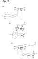
- the moving speed of the mount table 107 is decelerated, and the shutter 34 is closed, so as to stop emitting the processing laser light component L2. Thereafter, as illustrated in Fig. 17(c) , the mount table 107 is stopped moving when the coordinate is separated from the left end of the object 1 by 25 mm.
- the movement control section 115 moves the laser processing unit 110 in the Z direction, such that the Z-coordinate of the converging lens 31 becomes 65 ⁇ m, for example. Then, while the converging lenses 31, 32 are arranged on the same line to cut 5, the movement control section 115 moves the mount table 107 leftward along the line to cut 5, i.e., relatively moves the converging lenses 31, 32 in the direction (downward cutting direction) from the left end to right end of the object 1. Along with this movement, the following operation is executed.
- the converging lens control section 105 causes the piezoelectric device 29 to reproduce the command voltage data C at the X-coordinate of the converging lens 32 in the already memorized command voltage data C, so as to operate the converging lens 32.
- the piezoelectric device 29 reproduces (reverse-reproduces) the memorized command voltage data C in the order in reverse to that at the time of acquisition, so as to operate the converging lens 32.
- the shutter 34 is opened, and the object 1 is irradiated with the processing laser light component L2 while locating a converging point within the object 1, so as to form a modified region at a position of 65 ⁇ m in the Z direction with reference to the front face 3 of the object 1.
- the converging lens control section 105 causes the piezoelectric device 28 to reproduce the command voltage data C at the X-coordinate of the converging lens 31 in the already memorized command voltage data C, so as to operate the converging lens 31.
- the piezoelectric device 28 reverse-reproduces the memorized command voltage data C, so as to operate the converging lens 31.
- the shutter 33 is opened, and the object 1 is irradiated with the processing laser light component L1 while locating a converging point within the object 1, so as to form a modified region at a position of 57 ⁇ m in the Z direction with reference to the front face 3 of the object 1.
- the shutter 34 is closed, so as to stop emitting the processing laser light component L2. Then, from the time when the X-coordinate of the converging lens 31 reaches the right end of the object 1, the moving speed of the mount table 107 is decelerated, and the shutter 33 is closed, so as to stop emitting the processing laser light component L1. Thereafter, as illustrated in Fig. 18(c) , the mount table 107 is stopped moving when the coordinate is separated from the right end of the object 1 by 25 mm.
- the movement control section 115 moves the laser processing unit 110 in the Z direction, so that the Z-coordinate of the converging lens 31 becomes 48 ⁇ m, for example. Then, while the converging lenses 31, 32 are arranged on the same line to cut 5, the movement control section 115 moves the mount table 107 rightward again along the line to cut 5. Along with this movement, the following operation is executed.
- the converging lens control section 105 causes the piezoelectric device 28 to reproduce the command voltage data C at the X-coordinate of the converging lens 31 in the already memorized command voltage data C, so as to operate the converging lens 31. Also, the shutter 33 is opened, and the object 1 is irradiated with the processing laser light component L1 while locating a converging point within the object 1, so as to form a modified region at a position of 48 ⁇ m in the Z direction with reference to the front face 3 of the object 1.
- the converging lens control section 105 causes the piezoelectric device 29 to reproduce the command voltage data C at the X-coordinate of the converging lens 32 in the already memorized command voltage data C, so as to operate the converging lens 32. Also, the shutter 34 is opened, and the object 1 is irradiated with the processing laser light component L2 while locating a converging point within the object 1, so as to form a modified region at a position of 38 ⁇ m in the Z direction with reference to the front face 3 of the object 1.
- the shutter 33 is closed, so as to stop emitting the processing laser light component L1.
- the moving speed of the mount table 107 is decelerated, and the shutter 34 is closed, so as to stop emitting the processing laser light component L2.
- the mount table 107 is stopped moving when the coordinate is separated from the right end of the object 1 by 25 mm.
- the movement control section 115 moves the laser processing unit 110 in the Z direction, so that the Z-coordinate of the converging lens 31 becomes 25 ⁇ m, for example. Then, while the converging lenses 31, 32 are arranged on the same line to cut 5, the movement control section 115 moves the mount table 107 leftward along the line to cut 5. Along with this movement, an operation similar to that in the above-mentioned first downward cutting is executed, so as to form modified regions at positions of 25 ⁇ m and 15 ⁇ m, respectively, with reference to the front face 3 of the object 1.
- the linearly polarized processing laser light L having a polarization direction in the X direction is emitted from the processing laser light source 101 and, after its polarization direction is changed by the half-wave plate 51, is made incident on the polarizing plate 52.
- the polarizing plate 52 splits the processing laser light L into the processing laser light component L1 whose polarization direction is the X direction and the processing laser light component L2 whose polarization direction is the Y direction.
- the half-wave plate 55 changes the processing laser light component L2 into linearly polarized light whose polarization direction is the X direction.
- the processing laser light L is split into components incident on the converging lenses 31, 32, respectively, as linearly polarized light whose polarization direction is the X direction.
- the movement control section 115 relatively moves the mount table 107 along the line to cut 5 in a state where the X direction substantially coincides with the line to cut 5
- the measuring laser light source 41 emits the measuring laser light L3
- the quadrant photodiode 42 detects the voltage value of the reflected light component L4
- the converging lens control section 105 drives the piezoelectric device 28 such that the voltage value becomes V0
- the converging lens 31 is operated in the Z direction such that the distance at the time of height setting is kept between the front face 3 of the object 1 and the converging lens 31.
- the command voltage having driven the piezoelectric device 28 is memorized in the converging lens control section 105 as command voltage data C associated with the X-coordinate.
- the converging lens control section 105 causes the piezoelectric device 29 to reproduce the command voltage data at the X-coordinate of the converging lens 32 in the memorized command voltage data C, and irradiates the object 1 with the processing laser light component L2 while operating the converging lens 32, so that the converging point of the processing laser light component L2 is located at a predetermined position with reference to the front face 3.
- the converging lens control section 105 causes the piezoelectric device 29 to reproduce the command voltage data C at the X-coordinate of the converging lens 32 in the already memorized command voltage data C, so as to operate the converging lens 32, and causes the piezoelectric device 28 to reproduce the command voltage data C at the X-coordinate of the converging lens 31 in the already memorized command voltage data C, so as to operate the converging lens 31. Therefore, at least two rows of modified regions can simultaneously be formed within the object 1, so that the number of repeating scans of the processing laser light along the same line to cut can be reduced when forming a plurality of rows of modified regions in the thickness direction of the object 1.
- this embodiment can shorten not only the time for forming modified layers in the laser processing but also takt time, thereby reducing the running cost.
- the half-wave plate 53 changes the polarization direction of the processing laser light L to a given direction as mentioned above, so that the polarization direction of the processing laser light L transmitted through the half-wave plate 53 becomes the given direction, whereby portions of light quantities of the processing laser light components L1, L2 split by the polarizing plate 52 can be adjusted arbitrarily.
- the mount table 107 is moved by the movement control section 115 in a state where the polarization directions of the processing laser light components L1, L2 substantially coincide with the line to cut 5.
- This makes it possible to efficiently form modified regions along the lines to cut. This is because the forming of modified regions by irradiation with the polarized processing laser light is accelerated in its polarization direction (has a property of expanding in the polarization direction of the laser light). Further, since the polarization directions of the laser light components L1, L2 substantially coincide with the lines to cut 5, the modified regions are restrained from being formed in directions other than those along the lines to cut 5, whereby the object 1 can precisely be cut along the lines to cut 5.
- this embodiment closes the shutter 33 when emitting the measuring laser light L3, so that the converging lens 31 does not converge the processing laser light component L1 toward the object 1, this is not restrictive.
- the shutter 33 may be opened, so that the converging lens 31 also converges the processing laser light component L1 toward the object 1, thereby forming modified regions within the object 1 with the processing laser light component L1 while detecting information about the displacement of the front face 3 of the object 1 (so-called real-time processing) as a matter of course.
- scans for performing tracing alone are unnecessary even when an even number of rows of modified regions are to be formed in the thickness direction of the object.
- the object 1 was processed with each of the laser processing apparatus 100 in accordance with the embodiment explained above and a conventional laser processing apparatus.
- the laser processing apparatus 100 in accordance with the embodiment was able to shorten takt time by about 40% with reference to that of the conventional processing apparatus, whereby the above-mentioned effect, i.e., the effect of shortening the time for forming the modified layers in the laser processing, has been verified.
- the displacement of the laser light irradiation surface 3 may be measured by providing the laser light source on the optical axis side of the converging lens 32 as a matter of course, or both of them may be provided as well.
- the laser processing apparatus 100 in accordance with the above-mentioned embodiment is equipped with two converging lenses 31, 32, it may comprise three or more lenses. Effects similar to those mentioned above are exhibited in the latter case as well.
- the converging lenses 31, 32 may be moved along the lines to cut as well.
- the processing laser light may be emitted under various conditions without being limited by pulse pitch width, output, and the like.
- the present invention makes it possible to provide a laser processing apparatus which can shorten the time required for forming a modified region within an object to be processed.
Landscapes
- Physics & Mathematics (AREA)
- Optics & Photonics (AREA)
- Engineering & Computer Science (AREA)
- Plasma & Fusion (AREA)
- Mechanical Engineering (AREA)
- Chemical & Material Sciences (AREA)
- Chemical Kinetics & Catalysis (AREA)
- General Chemical & Material Sciences (AREA)
- Oil, Petroleum & Natural Gas (AREA)
- Laser Beam Processing (AREA)
- Re-Forming, After-Treatment, Cutting And Transporting Of Glass Products (AREA)
- Dicing (AREA)
Abstract
Description
- The present invention relates to a laser processing apparatus for cutting a planar object to be processed along a line to cut.
- Known as a conventional laser processing apparatus is one which irradiates a planar object to be processed with processing laser light while locating a converging point within the object, so as to form a modified region to become a cutting start point within the object along a line to cut the object (see, for example, Patent Literature 1).
- Patent Literature 1: Japanese Patent Application Laid-Open No.
2004-343008 - Meanwhile, the following is necessary for a laser processing apparatus such as the one mentioned above to cut a relatively thick object to be processed having a thickness of 100 µm or more, for example. That is, for forming a modified region accurately at a predetermined position distanced from a laser light irradiation surface of the object, it is necessary to emit (trace) measuring laser light for measuring a displacement of the laser light irradiation surface along the line to cut before forming the modified region by irradiation with the processing laser light. Further, for accurately cutting the object, a plurality of rows of modified regions are required to be formed in the thickness direction of the object, which makes it necessary to scan the processing laser light along the same line to cut a plurality of times according to the number of rows of modified regions. Therefore, it may take a long time for the laser processing apparatus such as the one mentioned above to form the modified regions within the object, thereby increasing the running cost.
- It is therefore an object of the present invention to provide a laser processing apparatus which can shorten the time required for forming a modified region within an object to be processed.
- For achieving the above-mentioned object, in one aspect, the laser processing apparatus in accordance with the present invention is a laser processing apparatus for irradiating a planar object to be processed with processing laser light while locating a converging point within the object, so as to form a modified region to become a cutting start point within the object along a line to cut the object, the apparatus comprising a mount table for mounting the object; a processing laser light source for emitting the processing laser light as linearly polarized light; a measuring laser light source for emitting measuring laser light for irradiating the object; a first half-wave plate for changing a polarization direction of the processing laser light emitted from the processing laser light source; a polarizing plate for splitting the processing laser light transmitted through the first half-wave plate into a processing laser light component having a polarization direction in a predetermined direction and a processing laser light component having a polarization direction in a direction intersecting the predetermined direction; a second half-wave plate for changing the polarization direction of the processing laser light component, split by the polarizing plate, having the polarization direction in the direction intersecting the predetermined direction into the predetermined direction; a first converging lens for converging the processing laser light component, split by the polarizing plate, having the polarization direction in the predetermined direction and the measuring laser light emitted from the measuring laser light source toward the object; a second converging lens, arranged in parallel with the first converging lens along the predetermined direction, for converging the processing laser light component, transmitted through the second half-wave plate, having the polarization direction in the predetermined direction toward the object; control means for detecting a reflected light component of the measuring laser light reflected by a laser light irradiation surface irradiated with the measuring laser light in the object so as to regulate a distance between the laser light irradiation surface and the second converging lens such that a converging point of the processing laser light converged by the second converging lens is located at a predetermined position with reference to the laser light irradiation surface; and moving means for relatively moving at least one of a pair of the first and second converging lenses and the mount table along the line to cut in a state where the predetermined direction substantially coincides with the line to cut.
- In another aspect, the laser processing apparatus in accordance with the present invention is a laser processing apparatus for irradiating a planar object to be processed with processing laser light while locating a converging point within the object, so as to form a modified region to become a cutting start point within the object along a line to cut the object, the apparatus comprising a mount table for mounting the object; a processing laser light source for emitting the processing laser light as linearly polarized light; a measuring laser light source for emitting measuring laser light for irradiating the object; a first half-wave plate for changing a polarization direction of the processing laser light emitted from the processing laser light source; a polarizing plate for splitting the processing laser light transmitted through the first half-wave plate into a processing laser light component having a polarization direction in a predetermined direction and a processing laser light component having a polarization direction in a direction intersecting the predetermined direction; a second half-wave plate for changing the polarization direction of the processing laser light component, split by the polarizing plate, having the polarization direction in the direction intersecting the predetermined direction into the predetermined direction; a first converging lens for converging the processing laser light component, transmitted through the second half-wave plate, having the polarization direction in the predetermined direction and the measuring laser light emitted from the measuring laser light source toward the object; a second converging lens, arranged in parallel with the first converging lens along the predetermined direction, for converging the processing laser light component, split by the polarizing plate, having the polarization direction in the predetermined direction toward the object; control means for detecting a reflected light component of the measuring laser light reflected by a laser light irradiation surface irradiated with the measuring laser light in the object so as to regulate a distance between the laser light irradiation surface and the second converging lens such that a converging point of the processing laser light converged by the second converging lens is located at a predetermined position with reference to the laser light irradiation surface; and moving means for relatively moving at least one of a pair of the first and second converging lenses and the mount table along the line to cut in a state where the predetermined direction substantially coincides with the line to cut.
- In the laser processing apparatus in accordance with the present invention, linearly polarized processing laser light is emitted from a processing laser light source, changes the polarization direction with a first half-wave plate, and then is incident on a polarizing plate. The polarizing plate splits the processing laser light into a processing light component having a polarization direction in a predetermined direction and a processing light component having a polarization direction in a direction intersecting the predetermined direction. The processing laser light component, split by the polarizing plate, having the polarization direction in the direction intersecting the predetermined direction changes the polarization direction to the predetermined direction because of a second half-wave plate. In other words, the linearly polarized processing laser light is split into respective components incident on the first and second converging lenses, while having the converging direction in the predetermined direction. Then, in this case, as at least one of the pair of first and second converging lenses and the mount table is relatively moved by the moving means along the line to cut in a state where the predetermined direction substantially coincides with the line to cut, for example, the measuring laser light is emitted from the measuring laser light source, and control means detects a reflected light component of the measuring laser light reflected by the laser light irradiation surface of the object, whereby the distance between the laser light irradiation surface and the second converging lens is regulated such that a converging point of the processing laser light converged by the second converging lens is located at a predetermined position with reference to the laser light irradiation surface. These make it possible to measure the displacement of the laser light irradiation surface with the measuring laser light and form the modified region with the processing laser light at the same time, whereby pretracing is unnecessary even when the object is relatively thick. This can shorten the time required for forming the modified region within the object.
- Preferably, the control means detects the reflected light component of the measuring laser light reflected by the laser light irradiation surface so as to regulate a distance between the laser light irradiation surface and the first converging lens such that a converging point of the processing laser light converged by the first converging lens is located at a predetermined position with reference to the laser light irradiation surface. In this case, as at least one of the pair of first and second converging lenses and the mount table is relatively moved by the moving means along the line to cut in a state where the predetermined direction substantially coincides with the line to cut, for example, the measuring laser light is emitted from the measuring laser light source, and the control means detects a reflected light component of the measuring laser light reflected by the laser light irradiation surface of the object, whereby the distance between the laser light irradiation surface and the first converging lens is regulated such that a converging point of the processing laser light converged by the first converging lens is located at a predetermined position with reference to the laser light irradiation surface, while the distance between the laser light irradiation surface and the second converging lens is regulated such that a converging point of the processing laser light converged by the second converging lens is located at a predetermined position with reference to the laser light irradiation surface. Therefore, at least two rows of modified regions can simultaneously be formed within the object. As a result, when forming a plurality of rows of modified regions in the thickness direction of the object, the number of repeating scans of the processing laser light along the same line to cut can be reduced.
- Preferably, the first half-wave plate changes the polarization direction of the processing laser light to a given direction. In this case, portions of light quantities of the processing laser light components split by the polarizing plate can be adjusted arbitrarily according to the polarization direction of the processing laser light transmitted through the first half-wave plate.
- Preferably, the apparatus further comprises an attenuator, arranged between the processing laser light source and the first half-wave plate in an optical path of the processing laser light, for adjusting a light quantity of the processing laser light. In this case, the attenuator can adjust the light quantity of the processing laser light incident on the first half-wave plate, so as to change the total output of the processing laser light freely.
- Preferably, the apparatus further comprises a shutter, arranged between the polarizing plate and the first converging lens in an optical path of the processing laser light, for blocking the processing laser light from being made incident on the first converging lens. In this case, closing the shutter can reliably and easily inhibit the first converging lens from converging the processing laser light toward the object. This is effective in particular when only the displacement measurement for the laser light irradiation surface with the first converging lens is carried out by using the first converging lens.
- There is also a case where the second converging lens is arranged in parallel with the first converging lens while being separated therefrom by a predetermined distance, and the control means executes control for operating the first converging lens such that the first converging lens is separated from the laser light irradiation surface by a constant distance and, while acquiring operation information concerning the operation, operating the second convergent lens according to the operation information and the predetermined distance, and control for operating the first converging lens according to the operation information acquired beforehand and operating the second converging lens according to the operation information acquired beforehand and the predetermined distance.
- The present invention makes it possible to provide a laser processing apparatus which can shorten the time required for forming a modified region within an object to be processed.
-
- [
Fig. 1 ] is a plan view of an object to be processed during laser processing by the laser processing apparatus in accordance with an embodiment; - [
Fig. 2 ] is a sectional view of the object taken along the line II-II ofFig. 1 ; - [
Fig. 3 ] is a plan view of the object after laser processing by the laser processing apparatus in accordance with the embodiment; - [
Fig. 4 ] is a sectional view of the object taken along the line IV-IV ofFig. 3 ; - [
Fig. 5 ] is a sectional view of the object taken along the line V-V ofFig. 3 ; - [
Fig. 6 ] is a plan view of the object cut by the laser processing apparatus in accordance with the embodiment; - [
Fig. 7 ] is a graph illustrating relationships between the field intensity and crack spot size in the laser processing apparatus in accordance with the embodiment; - [
Fig. 8 ] is a sectional view of the object in a first step of the laser processing apparatus in accordance with the embodiment; - [
Fig. 9 ] is a sectional view of the object in a second step of the laser processing apparatus in accordance with the embodiment; - [
Fig. 10 ] is a sectional view of the object in a third step of the laser processing apparatus in accordance with the embodiment; - [
Fig. 11 ] is a sectional view of the object in a fourth step of the laser processing apparatus in accordance with the embodiment; - [
Fig. 12 ] is a view illustrating a photograph of a cut section in a part of a silicon wafer cut by the laser processing apparatus in accordance with the embodiment; - [
Fig. 13 ] is a graph illustrating relationships between the laser light wavelength and the transmittance within a silicon substrate in the laser processing apparatus in accordance with the embodiment; - [
Fig. 14 ] is a front view illustrating an object to be processed; - [
Fig. 15 ] is a partial sectional view taken along the line XV-XV ofFig. 14 ; - [
Fig. 16 ] is a schematic view illustrating the laser processing apparatus in accordance with an embodiment of the present invention; - [
Fig. 17 ] is a partial sectional view taken along the line XVII-XVII ofFig. 14 for explaining a laser processing method by the laser processing apparatus ofFig. 16 ; - [
Fig. 18 ] is a partial sectional view taken along the line XVII-XVII ofFig. 14 for explaining the laser processing method subsequent toFig. 17 ; and - [
Fig. 19 ] is a partial sectional view taken along the line XVII-XVII ofFig. 14 for explaining the laser processing method subsequent toFig. 18 . - 1... object to be processed; 3...front face (laser light entrance surface); 5...like to cut; 7...modified region; 31... converging lens (first converging lens); 32...converging lens (second converging lens); 33, 34...shutter; 41...measuring laser light source; 42...quadrant photodiode (displacement acquiring means); 51...half-wave plate (first wave plate); 52...polarizing plate; 55...half-wave plate (second wave plate); 101...processing laser light source; 102...attenuator; 105...converging lens control section (control means); 107...mount table; 115...movement control section (moving means); L, L1, L2 ... processing laser light; L3 ... measuring laser light; L4 ... reflected light; P...converging point
- In the following, a preferred embodiment of the present invention will be explained in detail with reference to the drawings. In the laser processing method in accordance with the embodiment, a phenomenon known as multiphoton absorption is used for forming a modified region within an object to be processed. Therefore, to begin with, a laser processing method for forming a modified region by the multiphoton absorption will be explained.
- A material becomes transparent when its absorption bandgap EG is greater than photon energy hv. Consequently, a condition under which absorption occurs in the material is hv > EG. However, even when optically transparent, the material generates absorption under a condition of nhv > EG (where n = 2, 3, 4, ...) if the intensity of laser light becomes very high. This phenomenon is known as multiphoton absorption. In the case of pulsed waves, the intensity of laser light is determined by the peak power density (W/cm2) of laser light at its converging point. The multiphoton absorption occurs under a condition where the peak power density is 1 × 10⁸ (W/cm2) or greater, for example. The peak power density is determined by (energy of laser light at the converging point per pulse)/(beam spot cross-sectional area of laser light × pulse width). In the case of continuous waves, the intensity of laser light is determined by the field intensity (W/cm2) of laser light at the converging point.
- The principle of the laser processing method in accordance with the embodiment using such multiphoton absorption will be explained with reference to
Figs. 1 to 6 . As illustrated inFig. 1 , on afront face 3 of a wafer-like (planar) object to be processed 1, a line to cut 5 for cutting theobject 1 exists. The line to cut 5 is a virtual line extending straight. As illustrated inFig. 2 , the laser processing method in accordance with this embodiment irradiates theobject 1 with laser light L while locating a converging point P therewithin under a condition generating multiphoton absorption, so as to form a modifiedregion 7. The converging point P is a position at which the laser light L is converged. The line to cut 5 may be curved instead of being straight, and may be a line actually drawn on theobject 1 without being restricted to the virtual line. - Then, the laser light L is relatively moved along the line to cut 5 (i.e., in the direction of arrow A in
Fig. 1 ), so as to shift the converging point P along the line to cut 5. Consequently, as illustrated inFigs. 3 to 5 , the modifiedregion 7 is formed along the line to cut 5 within theobject 1, and becomes a cuttingstart region 8. The cuttingstart region 8 refers to a region which becomes a start point for cutting (fracturing) when theobject 1 is cut. The cuttingstart region 8 may be made by forming the modifiedregion 7 either continuously or intermittently. - In the laser processing method in accordance with this embodiment, the
front face 3 of theobject 1 hardly absorbs the laser light L and thus does not melt. - Forming the cutting
start region 8 within theobject 1 makes it easier to generate fractures from the cuttingstart region 8 acting as a start point, whereby theobject 1 can be cut with a relatively small force as illustrated inFig. 6 . Therefore, theobject 1 can be cut with a high precision without generating unnecessary fractures on thefront face 3 of theobject 1. - There seem to be the following two ways of cutting the
object 1 from the cuttingstart region 8 acting as a start point. One is where an artificial force is applied to theobject 1 after the cuttingstart region 8 is formed, so that theobject 1 fractures from the cuttingstart region 8 acting as a start point, whereby theobject 1 is cut. This is the cutting in the case where theobject 1 has a large thickness, for example. Applying an artificial force refers to exerting a bending stress or shear stress to theobject 1 along the cuttingstart region 8, or generating a thermal stress by applying a temperature difference to theobject 1, for example. The other is where the forming of the cuttingstart region 8 causes theobject 1 to fracture naturally in its cross-sectional direction (thickness direction) from the cuttingstart region 8 acting as a start point, thereby cutting theobject 1. This becomes possible if the cuttingstart region 8 is formed by one row of the modifiedregion 7 when theobject 1 has a small thickness, or if the cuttingstart region 8 is formed by a plurality of rows of the modifiedregion 7 in the thickness direction when theobject 1 has a large thickness. Even in this naturally fracturing case, fractures do not extend onto thefront face 3 at a portion corresponding to an area not formed with the cuttingstart region 8 in the part to cut, so that only the portion corresponding to the area formed with the cuttingstart region 8 can be cleaved, whereby cleavage can be controlled well. Such a cleaving method with a favorable controllability is very effective, since theobject 1 to be processed such as a silicon wafer has recently been apt to decrease its thickness. - The modified region formed by multiphoton absorption in the laser processing method in accordance with this embodiment encompasses the following cases (1) to (3):
- (1) Case where the modified region is a crack region including one or a plurality of cracks
An object to be processed (e.g., glass or a piezoelectric material made of LiTaO3) is irradiated with laser light while locating a converging point therewithin under a condition with a field intensity of at least 1 × 10⁸ (W/cm2) at the converging point and a pulse width of 1 µs or less. This magnitude of pulse width is a condition under which a crack region can be formed only within the object while generating multiphoton absorption without causing unnecessary damages to the front face of the object. This generates a phenomenon of optical damage by multiphoton absorption within the object. This optical damage induces a thermal distortion within the object, thereby forming a crack region therewithin. The upper limit of field intensity is 1 × 10¹² (W/cm2), for example. The pulse width is preferably 1 ns to 200 ns, for example. The forming of a crack region by multiphoton absorption is disclosed, for example, in "Internal Marking of Glass Substrate with Solid-state Laser", Proceedings of the 45th Laser Materials Processing Conference (December, 1998), pp. 23-28. - The inventors determined the relationship between field intensity and crack size by an experiment. The following are conditions of the experiment.
-
- (A) Object to be processed: Pyrex (registered trademark) glass (with a thickness of 700 µm)
- (B) Laser
Light source: semiconductor laser pumping Nd:YAG laser
Wavelength: 1064 nm
Laser light spot cross-sectional area: 3.14 × 10⁻⁸ cm2
Oscillation mode: Q-switched pulse
Repetition frequency: 100 kHz
Pulse width: 30 ns
Output: output < 1 mJ/pulse
Laser light quality: TEM00
Polarizing property: linear polarization - (C) Converging lens
Transmittance at a laser light wavelength: 60% - (D) Moving rate of the mount table mounting the object: 100 mm/sec
- The laser light quality of TEM00 means that the converging characteristic is so high that convergence to about the wavelength of laser light is possible.
-
Fig. 7 is a graph illustrating the results of the above-mentioned experiment. The abscissa indicates the peak power density. Since the laser light is pulsed laser light, the field intensity is represented by the peak power density. The ordinate indicates the size of a crack part (crack spot) formed within the object by one pulse of laser light. Crack spots gather to yield a crack region. The crack spot size is the size of a part yielding the maximum length among forms of crack spots. Data represented by black circles in the graph refer to a case where the converging lens (C) has a magnification of x 100 and a numerical aperture (NA) of 0.80. On the other hand, data represented by whitened circles in the graph refer to a case where the converging lens (C) has a magnification of x50 and a numerical aperture (NA) of 0.55. Crack spots are seen to occur within the object from when the peak power density is about 1011 (W/cm2) and become greater as the peak power density increases. - A mechanism by which the object to be processed is cut by forming a crack region will now be explained with reference to
Figs. 8 to 11 . As illustrated inFig. 8 , theobject 1 is irradiated with laser light L while the converging point P is located within theobject 1 under a condition where multiphoton absorption occurs, so as to form acrack region 9 therewithin along a line to cut. Thecrack region 9 is a region containing one or a plurality of cracks. Thus formedcrack region 9 becomes a cutting start region. A crack further grows from thecrack region 9 acting as a start point (i.e., from the cutting start region acting as a start point) as illustrated inFig. 9 , and reaches thefront face 3 andrear face 21 of theobject 1 as illustrated inFig. 10 , whereby theobject 1 fractures and is consequently cut as illustrated inFig. 11 . The crack reaching thefront face 3 andrear face 21 of theobject 1 may grow naturally or as a force is applied to theobject 1. - (2) Case where the modified region is a molten processed region
An object to be processed (e.g., semiconductor material such as silicon) is irradiated with laser light while locating a converging point within the object under a condition with a field intensity of at least 1 × 10⁸ (W/cm2) at the converging point and a pulse width of 1 µs or less. As a consequence, the inside of the object is locally heated by multiphoton absorption. This heating forms a molten processed region within the object. The molten processed region encompasses regions once molten and then re-solidified, regions just in a molten state, and regions in the process of being re-solidified from the molten state, and can also be referred to as a region whose phase has changed or a region whose crystal structure has changed. The molten processed region may also be referred to as a region in which a certain structure changes to another structure among monocrystal, amorphous, and polycrystal structures. For example, it means a region having changed from the monocrystal structure to the amorphous structure, a region having changed from the monocrystal structure to the polycrystal structure, or a region having changed from the monocrystal structure to a structure containing amorphous and polycrystal structures. When the object to be processed is of a silicon monocrystal structure, the molten processed region is an amorphous silicon structure, for example. The upper limit of field intensity is 1 × 10¹² (W/cm2), for example. The pulse width is preferably 1 ns to 200 ns, for example. - By an experiment, the inventors verified that a molten processed region was formed within a silicon wafer (semiconductor substrate). The following are conditions of the experiment.
-
- (A) Object to be processed: silicon wafer (with a thickness of 350 µm and an outer diameter of 4 inches)
- (B) Laser
Light source: semiconductor laser pumping Nd:YAG laser
Wavelength: 1064 nm
Laser light spot cross-sectional area: 3.14 × 10⁻⁸ cm2
Oscillation mode: Q-switched pulse
Repetition frequency: 100 kHz
Pulse width: 30 ns
Output: 20 µJ/pulse
Laser light quality: TEM00
Polarizing property: linear polarization - (C) Converging lens
Magnification: x50
N.A.: 0.55
Transmittance at a laser light wavelength: 60% - (D) Moving rate of the mount table mounting the object: 100 mm/sec
-
Fig. 12 is a view illustrating a photograph of a cross section of a part of a silicon wafer cut by laser processing under the conditions mentioned above. A molten processedregion 13 is formed within thesilicon wafer 11. The molten processedregion 13 formed under the above-mentioned conditions has a size of about 100 µm in the thickness direction. - The fact that the molten processed
region 13 is formed by multiphoton absorption will now be explained.Fig. 13 is a graph illustrating relationships between the laser light wavelength and the transmittance within the silicon substrate. Here, the respective reflected components on the front and rear sides of the silicon substrate are eliminated, so as to represent the internal transmittance alone. The respective relationships are illustrated in the cases where the thickness t of the silicon substrate is 50 µm, 100 µm, 200 µm, 500 µm, and 1000 µm. - For example, at the Nd:YAG laser wavelength of 1064 nm, the laser light appears to be transmitted through the silicon substrate by at least 80% when the silicon substrate has a thickness of 500 µm or less. Since the
silicon wafer 11 illustrated inFig. 12 has a thickness of 350 µm, the molten processedregion 13 caused by multiphoton absorption is formed near the center of thesilicon wafer 11, i.e., at a part distanced from the front face by 175 µm. The transmittance in this case is 90% or more with reference to a silicon wafer having a thickness of 200 µm, whereby the laser light is absorbed only slightly within thesilicon wafer 11 but is substantially transmitted therethrough. This means that the molten processedregion 13 is formed within thesilicon wafer 11 not by the absorption of laser light within the silicon wafer 11 (i.e., not by usual heating with the laser light) but by multiphoton absorption. The forming of a molten processed region by multiphoton absorption is disclosed, for example, in "Ultrashort Pulse Laser Microprocessing of Silicon", Preprints of the National Meetings of Japan Welding Society, Vol. 66 (April, 2000), pp. 72-73. - A fracture is generated in a silicon wafer from a cutting start region formed by a molten processed region, acting as a start point, in a cross-sectional direction, and reaches the front and rear faces of the silicon wafer, whereby the silicon wafer is cut. The fracture reaching the front and rear faces of the silicon wafer may grow naturally or as a force is applied to the silicon wafer. The fracture naturally growing from the cutting start region to the front and rear faces of the silicon wafer encompasses a case where the fracture grows from a state in which the molten processed region forming the cutting start region is molten and a case where the fracture grows when the molten processed region forming the cutting start region is re-solidified from the molten state. In either case, the molten processed region is formed only within the silicon wafer, and thus is present only within the cut section after cutting as illustrated in
Fig. 12 . When a cutting start region is thus formed within the object by a molten processed region, unnecessary fractures deviating from a cutting start region line are harder to occur at the time of cleaving, whereby cleavage control becomes easier. Here, the molten processed region may be formed not only by multiphoton absorption but also by other absorption actions. - (3) Case where the modified region is a refractive index change region
An object to be processed (e.g., glass) is irradiated with laser light while locating a converging point within the object under a condition with a field intensity of at least 1 × 10⁸ (W/cm2) at the converging point and a pulse width of 1 ns or less. When multiphoton absorption is generated within the object with a very short pulse width, the energy caused by multiphoton absorption is not converted into thermal energy, whereby an eternal structure change such as ion valence change, crystallization, or orientation polarization is induced within the object, thus forming a refractive index change region. The upper limit of field intensity is 1 × 10¹² (W/cm2), for example. The pulse width is preferably 1 ns or less, for example, more preferably 1 ps or less. The forming of a refractive index change region by multiphoton absorption is disclosed, for example, in "Forming of Photoinduced Structure within Glass by Femtosecond Laser Irradiation", Proceedings of the 42nd Laser Materials Processing Conference (November, 1997), pp. 105-111. - Though the cases (1) to (3) are explained in the foregoing as a modified region formed by multiphoton absorption, a cutting start region may be formed as follows while taking account of the crystal structure of a wafer-like object to be processed, its cleavage characteristic, and the like, whereby the object can be cut with a favorable precision by a smaller force from the cutting start region acting as a start point.
- That is, in the case of a substrate made of a monocrystal semiconductor having a diamond structure such as silicon, it will be preferred if a cutting start region is formed in a direction extending along a (111) plane (first cleavage plane) or a (110) plane (second cleavage plane). In the case of a substrate made of a group III-V compound semiconductor of sphalerite structure such as GaAs, it will be preferred if a cutting start region is formed in a direction extending along a (110) plane. In the case of a substrate having a crystal structure of hexagonal system such as sapphire (Al2O3), it will be preferred if a cutting start region is formed in a direction extending along a (1120) plane (A plane) or a (1100) plane (M plane) while using a (0001) plane (C plane) as a principal plane.
- When the substrate is formed with an orientation flat in a direction to be formed with the above-mentioned cutting start region (e.g., a direction extending along a (111) plane in a monocrystal silicon substrate) or a direction orthogonal to the former direction, the cutting start region extending in the direction to be formed with the cutting start region can be formed easily and accurately with reference to the orientation flat.
- The preferred embodiment of the present invention will now be explained.
- As illustrated in
Figs. 14 and15 , an object to be processed 1 comprises asilicon wafer 11 having a thickness of 300 µm and a diameter of 8 inches and afunctional device layer 16 which is formed on afront face 11a of thesilicon wafer 11 while including a plurality offunctional devices 15. - A number of
functional devices 15, examples of which include semiconductor operating layers formed by crystal growth, light-receiving devices such as photodiodes, light-emitting devices such as laser diodes, and circuit devices formed as circuits, are formed like a matrix in directions parallel and perpendicular to anorientation flat 6 of thesilicon wafer 11. Such an object to be processed 1 is cut along lines to cut 5 which are set like grids passing between the functional devices adjacent to each other, so as to become chips each having a size of 1 mm × 1 mm, for example. - As illustrated in
Fig. 16 , alaser processing apparatus 100 irradiates the planar object to be processed 1 with laser light (processing laser light) L while locating a converging point within theobject 1, so as to form a plurality of rows of modified regions to become a cutting start point within theobject 1 along thelines 5 to cut theobject 1. - The
laser processing apparatus 100 comprises a mount table 107 for mounting theobject 1 horizontally, alaser unit 110, and a movement control section (moving means) 115 for moving the mount table 107 andlaser unit 110. Themovement control section 115 moves the mount table 107 in horizontal directions (X and Y directions) and thelaser unit 110 in vertical directions (Z directions). - The
laser unit 110 is equipped with a processinglaser light source 101 for pulse-oscillating linearly polarized processing laser light L having a polarization direction in the X direction (predetermined direction). The processing laser light L emitted from the processinglaser light source 101 passes through anattenuator 102 for adjusting the light quantity of the processing laser light L, so as to be guided to aseparator 103 for splitting it into a linearly polarized processing laser light component L1 having a polarization direction in the X direction and a linearly polarized processing laser light component L2 having a polarization direction in the Y direction (direction intersecting the predetermined direction). - The split processing laser light component L1 is successively guided to a
shutter 33 for transmitting or blocking the processing laser light component L1, abeam expander 35 for expanding its beam size, and adichroic mirror 48, and then is converged by a converging lens (first converging lens) 31, so as to irradiate theobject 1. The converginglens 31 is one which converges the processing laserlight component L 1 and measuring laser light L3, which will be explained later, toward theobject 1. Apiezoelectric device 28 is attached to the converginglens 31, so as to adjust the Z-directional position of the converginglens 31. Thedichroic mirror 48 transmits the processing laser light component L1 therethrough but reflects the measuring laser light L3 and its reflected light component L4, which will be explained later. - On the other hand, the split processing laser light component L2 is successively guided to a
mirror 22, ashutter 34, and abeam expander 36, so as to be turned into linearly polarized light having a polarization direction in the X direction by anattenuator 104, and then is converged by a converging lens (second converging lens) 32, so as to irradiate theobject 1. The converginglens 32, which is arranged in parallel with the converginglens 31 while being separated therefrom by a predetermined distance D in the X direction, converges the processing laser light component L2 toward theobject 1. Here, the distance D is 35 mm. Apiezoelectric device 29 is attached to the converginglens 32 as with the converginglens 31, so as to adjust the Z-directional position of the converginglens 32. - The
laser unit 110 also has a measuringlaser light source 41 using a laser diode, for example. The measuringlaser light source 41 emits the measuring laser light L3 for irradiating theobject 1, so as to measure the displacement of thefront face 3 of theobject 1, whereby a modified region can accurately be formed at a desirable position within theobject 1. The measuring laser light L3 emitted from the measuringlaser light source 41 is successively reflected by amirror 46 and ahalf mirror 47, so as to be guided to thedichroic mirror 48. Then, the measuring laser light L3 advances downward on the optical axis of the processing laser light component L1, so as to be converged by the converginglens 31, thus irradiating theobject 1. The reflected light component L4 of the measuring laser light L3 reflected by the front face (laser light irradiation surface) 3 of theobject 1 is made incident on the converginglens 31 again, so as to advance upward on the optical axis of the processing laser light component L1, and then is reflected by thedichroic mirror 48 and transmitted through thehalf mirror 47. - The reflected light component L4 of the measuring laser light transmitted through the
half mirror 47 is provided with astigmatism and converged by a shapingoptical system 49 composed of a cylindrical lens and a planoconvex lens, so as to irradiate aquadrant photodiode 42 constructed by equally dividing a photodiode into four, thereby forming a converged light image on a light-receiving surface of thequadrant photodiode 42. In response to the displacement of thefront face 3 of theobject 1, the converged light image varies because of the astigmatism added thereto by the shapingoptical system 49. Hence, thequadrant photodiode 42 acquires displacement information concerning the displacement of thefront face 3 as a voltage value. A converging lens control section (control means) 105 is connected to thequadrant photodiode 42. The above-mentionedpiezoelectric devices lens control section 105. The converginglens control section 105 controls the driving of thepiezoelectric devices lenses front face 3. - Specifically, the converging
lens control section 105 executes control for operating the converginglens 31 such that thefront face 3 of theobject 1 and the converginglens 31 are separated from each other by a fixed distance therebetween according to the voltage value acquired by thequadrant photodiode 42 and, while acquiring operation information concerning this operation, operating the converginglens 32 according to the operation information and the distance D. - More specifically, the converging
lens control section 105 executes the following control. In a state where the converginglenses piezoelectric device 28 is driven such that the voltage value acquired by thequadrant photodiode 42 becomes constant, thus operating the converginglens 31 such as to keep a constant distance between thefront face 3 of theobject 1 and the converginglens 31. Also, while memorizing a command voltage having driven thepiezoelectric device 28 as command voltage data in association with the coordinate along the line to cut 5, the command voltage data at the X-coordinate of the converging lens 32 (the coordinate obtained by adding the distance D to the X-coordinate of the converging lens 31) is reproduced by thepiezoelectric device 29, so as to operate the converginglens 32. In other words, thepiezoelectric device 29 reproduces the memorized voltage data with a delay required for relatively moving the mount table 107 by the distance D, so as to operate the converginglens 32. - The converging
lens control section 105 executes control for operating the converginglens 31 according to the operation information acquired beforehand and operating the converginglens 32 according to the operation information acquired beforehand and the distance D. - More specifically, the converging
lens control section 105 executes the following control. In the state where the converginglenses lens 31 in the already memorized command voltage data is reproduced by thepiezoelectric device 28, so as to operate the converginglens 31. Also, the voltage data at the X-coordinate of the converginglens 32 in the already memorized command voltage data is reproduced by thepiezoelectric device 29, so as to operate the converginglens 32. - Meanwhile, the
laser processing apparatus 100 is provided with theseparator 103 as mentioned above. Theseparator 103 has a half-wave plate (first half-wave plate) 51 and apolarizing plate 52. Specifically, the half-wave plate 51 andpolarizing plate 52 are arranged in this order on the optical axis of the processing laser light L. - The half-
wave plate 51 is rotatable about the optical axis of the processing laser light L and thus can change the polarization direction of the processing laser light L to a given direction. That is, the half-wave plate 51 lets the processing laser light L whose polarization direction is in the X direction to have a polarization direction forming an angle of 45° or 60° with the X axis within a horizontal plane (X-Y plane), for example. - The
polarizing plate 52 splits the processing laser light L into the processing laser light component L1 having a polarization direction in the X direction and the processing laser light component L2 having a polarization direction in the Y direction. Specifically, in the processing laser light L, thepolarizing plate 52 transmits therethrough a processing laser light component having a polarization direction in the X direction as the processing laser light component L1 toward the converginglens 31, while reflecting a processing laser light component having a polarization direction in the Y direction as the processing laser light component L2 toward the converginglens 32. - The
laser processing apparatus 100 is provided with theattenuators attenuator 102 has a half-wave plate 53 and apolarizing plate 54, which are arranged on the optical axis of the processing laser light L in this order in the emitting direction of the processing laser light L. In theattenuator 102, the half-wave plate 53 changes the direction of polarization of the processing laser light L, while thepolarizing plate 54 transmits only the processing laser light L having the polarization direction in the X direction. Hence, theattenuator 102 mainly functions as a so-called attenuator which regulates the light quantity of the processing laser light L, so as to freely adjust (change) the total output of the processing laser light L. - The
attenuator 104 has a half-wave plate (second half-wave plate) 55 and apolarizing plate 56, which are arranged on the optical axis of the processing laser light component L2 in this order in the emitting direction of the processing laser light component L2. The half-wave plate 55 changes the polarization direction of the laser light component to the X direction as in the processing laser light component L1. Hence, the half-wave plate 55 mainly functions as a so-called polarizer which makes the polarization direction of the processing laser light component L2 identical to that of the processing laser light component L1. Thepolarizing plate 56 transmits therethrough only the processing laser light component L2 having the polarization direction in the X direction toward the converginglens 32. - When cutting the
object 1 with thelaser processing apparatus 100 explained in the foregoing, an expandable tape, for example, is initially attached to therear face 21 of theobject 1, which is then mounted on the mount table 107. Subsequently, theobject 1 is irradiated with the processing laser light L from thefront face 3 while locating a converging point within thesilicon wafer 11, so as to form a modified region to become a cutting start point within theobject 1 along each line to cut 5. Then, the expandable tape is expanded. As a consequence, theobject 1 is accurately cut into thefunctional devices 15 along the line to cut 5 from the modified region acting as the cutting start point, whereby a plurality of semiconductor chips are separated from each other. The modified region may include not only the molten processed region but also crack regions and the like. - The forming of the modified region mentioned above will now be explained in more detail. Here, the following explanation will assume that the direction along the line to cut 5 and the thickness direction of the
object 1 are the X direction (X-coordinate) and Z direction (Z-coordinate), respectively, as in the above. - First, while being focused on a reticle image, for example, projected on the
front face 3 of theobject 1, the measuring laser light L3 is emitted, the reflected light component L4 of the measuring laser light L3 reflected by thefront face 3 is detected as a voltage value, and thus detected voltage value V0 is memorized. While using the Z-coordinate of the converginglens 31 at this time as a reference value (0 µm), the direction from thefront face 3 side to therear face 21 side is taken as a positive direction. - Subsequently, as illustrated in
Fig. 17(a) , the mount table 107 is moved such that the X-coordinate of the converginglens 31 becomes an X-coordinate distanced from the right end of theobject 1 by 25 mm, for example. The X-coordinate of the converginglens 31 is an acceleration/deceleration distance of the mount table 107 required until the mount table 107 attains a constant moving speed. The acceleration/deceleration distance may be set as appropriate according to the moving speed of the mount table 107. - Subsequently, while the converging
lenses movement control section 115 moves the mount table 107 rightward along the line to cut 5, i.e., relatively moves the converginglenses object 1. The following operation is executed along with this movement. - As illustrated in
Fig. 17(b) , the measuringlaser light source 41 emits the measuring laser light L3, thequadrant photodiode 42 detects the voltage value of the reflected light component L4, the converginglens control section 105 drives thepiezoelectric device 28 such that this voltage value becomes the voltage value V0, and the converginglens 31 is operated in the Z direction such that the distance between thefront face 3 of theobject 1 and the converginglens 31 is kept at that at the time of height setting. Also, the command voltage having driven thepiezoelectric device 28 is memorized (stored) in association with the X-coordinate as command voltage data C in the converginglens control section 105. At the time of memorization, theshutter 33 is closed, whereby the converginglens 31 is reliably and easily inhibited from letting out the processing laser light L1 when emitting the measuring laser light L3. This is effective in particular when only the displacement of thefront face 3 is measured by the measuring laser light L3 with the converginglens 31. - From the time when the X-coordinate of the converging
lens 32 reaches the right end of the object 1 (i.e., the X-coordinate of the converginglens 31 reaches a position separated leftward from the right end of theobject 1 by the distance D), the converginglens control section 105 causes thepiezoelectric device 29 to reproduce the command voltage data at the X-coordinate of the converginglens 32 in the memorized command voltage data C, so as to operate the converginglens 32. Also, as illustrated inFig. 17(b) , theshutter 34 is opened, and theobject 1 is irradiated with the processing laser light L2 while locating a converging point within theobject 1, so as to form a modified region at a position of 73 µm in the Z direction with reference to thefront face 3 of theobject 1. - From the time when the X-coordinate of the converging
lens 32 reaches the left end of theobject 1, the moving speed of the mount table 107 is decelerated, and theshutter 34 is closed, so as to stop emitting the processing laser light component L2. Thereafter, as illustrated inFig. 17(c) , the mount table 107 is stopped moving when the coordinate is separated from the left end of theobject 1 by 25 mm. - Subsequently, the
movement control section 115 moves thelaser processing unit 110 in the Z direction, such that the Z-coordinate of the converginglens 31 becomes 65 µm, for example. Then, while the converginglenses movement control section 115 moves the mount table 107 leftward along the line to cut 5, i.e., relatively moves the converginglenses object 1. Along with this movement, the following operation is executed. - As illustrated in
Fig. 18(a) , from the time when the X-coordinate of the converginglens 32 reaches the left end of theobject 1, the converginglens control section 105 causes thepiezoelectric device 29 to reproduce the command voltage data C at the X-coordinate of the converginglens 32 in the already memorized command voltage data C, so as to operate the converginglens 32. In other words, thepiezoelectric device 29 reproduces (reverse-reproduces) the memorized command voltage data C in the order in reverse to that at the time of acquisition, so as to operate the converginglens 32. Also, theshutter 34 is opened, and theobject 1 is irradiated with the processing laser light component L2 while locating a converging point within theobject 1, so as to form a modified region at a position of 65 µm in the Z direction with reference to thefront face 3 of theobject 1. - As illustrated in
Fig. 18(b) , from the time when the X-coordinate of the converginglens 31 reaches the left end of theobject 1, the converginglens control section 105 causes thepiezoelectric device 28 to reproduce the command voltage data C at the X-coordinate of the converginglens 31 in the already memorized command voltage data C, so as to operate the converginglens 31. In other words, thepiezoelectric device 28 reverse-reproduces the memorized command voltage data C, so as to operate the converginglens 31. Also, theshutter 33 is opened, and theobject 1 is irradiated with the processing laser light component L1 while locating a converging point within theobject 1, so as to form a modified region at a position of 57 µm in the Z direction with reference to thefront face 3 of theobject 1. - From the time when the X-coordinate of the converging
lens 32 reaches the right end of theobject 1, theshutter 34 is closed, so as to stop emitting the processing laser light component L2. Then, from the time when the X-coordinate of the converginglens 31 reaches the right end of theobject 1, the moving speed of the mount table 107 is decelerated, and theshutter 33 is closed, so as to stop emitting the processing laser light component L1. Thereafter, as illustrated inFig. 18(c) , the mount table 107 is stopped moving when the coordinate is separated from the right end of theobject 1 by 25 mm. - Subsequently, the
movement control section 115 moves thelaser processing unit 110 in the Z direction, so that the Z-coordinate of the converginglens 31 becomes 48 µm, for example. Then, while the converginglenses movement control section 115 moves the mount table 107 rightward again along the line to cut 5. Along with this movement, the following operation is executed. - As illustrated in
Fig. 19(a) , from when the X-coordinate of the converginglens 31 reaches the right end of theobject 1, the converginglens control section 105 causes thepiezoelectric device 28 to reproduce the command voltage data C at the X-coordinate of the converginglens 31 in the already memorized command voltage data C, so as to operate the converginglens 31. Also, theshutter 33 is opened, and theobject 1 is irradiated with the processing laser light component L1 while locating a converging point within theobject 1, so as to form a modified region at a position of 48 µm in the Z direction with reference to thefront face 3 of theobject 1. - As illustrated in
Fig. 19(b) , from when the X-coordinate of the converginglens 32 reaches the right end of theobject 1, the converginglens control section 105 causes thepiezoelectric device 29 to reproduce the command voltage data C at the X-coordinate of the converginglens 32 in the already memorized command voltage data C, so as to operate the converginglens 32. Also, theshutter 34 is opened, and theobject 1 is irradiated with the processing laser light component L2 while locating a converging point within theobject 1, so as to form a modified region at a position of 38 µm in the Z direction with reference to thefront face 3 of theobject 1. - From the time when the X-coordinate of the converging
lens 31 reaches the left end of theobject 1, theshutter 33 is closed, so as to stop emitting the processing laser light component L1. Then, from the time when the X-coordinate of the converginglens 32 reaches the left end of theobject 1, the moving speed of the mount table 107 is decelerated, and theshutter 34 is closed, so as to stop emitting the processing laser light component L2. Thereafter, as illustrated inFig. 19(c) , the mount table 107 is stopped moving when the coordinate is separated from the right end of theobject 1 by 25 mm. - Subsequently, the
movement control section 115 moves thelaser processing unit 110 in the Z direction, so that the Z-coordinate of the converginglens 31 becomes 25 µm, for example. Then, while the converginglenses movement control section 115 moves the mount table 107 leftward along the line to cut 5. Along with this movement, an operation similar to that in the above-mentioned first downward cutting is executed, so as to form modified regions at positions of 25 µm and 15 µm, respectively, with reference to thefront face 3 of theobject 1. - The foregoing forms a plurality of rows of modified regions, which become cutting start regions, in the thickness direction of the
object 1 along the lines to cut 5 (seeFig. 14 ). - Thus, in this embodiment, the linearly polarized processing laser light L having a polarization direction in the X direction is emitted from the processing
laser light source 101 and, after its polarization direction is changed by the half-wave plate 51, is made incident on thepolarizing plate 52. Thepolarizing plate 52 splits the processing laser light L into the processing laser light component L1 whose polarization direction is the X direction and the processing laser light component L2 whose polarization direction is the Y direction. Then, the half-wave plate 55 changes the processing laser light component L2 into linearly polarized light whose polarization direction is the X direction. Hence, the processing laser light L is split into components incident on the converginglenses - As in the above-mentioned first upward cutting, as the
movement control section 115 relatively moves the mount table 107 along the line to cut 5 in a state where the X direction substantially coincides with the line to cut 5, the measuringlaser light source 41 emits the measuring laser light L3, thequadrant photodiode 42 detects the voltage value of the reflected light component L4, the converginglens control section 105 drives thepiezoelectric device 28 such that the voltage value becomes V0, and the converginglens 31 is operated in the Z direction such that the distance at the time of height setting is kept between thefront face 3 of theobject 1 and the converginglens 31. Also, the command voltage having driven thepiezoelectric device 28 is memorized in the converginglens control section 105 as command voltage data C associated with the X-coordinate. The converginglens control section 105 causes thepiezoelectric device 29 to reproduce the command voltage data at the X-coordinate of the converginglens 32 in the memorized command voltage data C, and irradiates theobject 1 with the processing laser light component L2 while operating the converginglens 32, so that the converging point of the processing laser light component L2 is located at a predetermined position with reference to thefront face 3. These make it possible to measure the displacement of thefront face 3 with the measuring laser light L3 and form modified regions with the processing laser light component L2 at the same time, whereby theobject 1 is not required to be traced beforehand even when it is relatively thick. - As in the above-mentioned first downward cutting and the like, as the
movement control section 115 relatively moves the mount table 107 along the line to cut 5 in a state where the X direction substantially coincides with the line to cut 5, the converginglens control section 105 causes thepiezoelectric device 29 to reproduce the command voltage data C at the X-coordinate of the converginglens 32 in the already memorized command voltage data C, so as to operate the converginglens 32, and causes thepiezoelectric device 28 to reproduce the command voltage data C at the X-coordinate of the converginglens 31 in the already memorized command voltage data C, so as to operate the converginglens 31. Therefore, at least two rows of modified regions can simultaneously be formed within theobject 1, so that the number of repeating scans of the processing laser light along the same line to cut can be reduced when forming a plurality of rows of modified regions in the thickness direction of theobject 1. - Hence, while it is necessary for a conventional laser processing apparatus to repeat scans including traces eight times when forming seven rows (odd rows) of modified regions in the thickness direction within the
object 1 along the line to cut 5, four scans (1/2 that of the above) suffice in this embodiment. Therefore, this embodiment can shorten not only the time for forming modified layers in the laser processing but also takt time, thereby reducing the running cost. - In this embodiment, the half-
wave plate 53 changes the polarization direction of the processing laser light L to a given direction as mentioned above, so that the polarization direction of the processing laser light L transmitted through the half-wave plate 53 becomes the given direction, whereby portions of light quantities of the processing laser light components L1, L2 split by thepolarizing plate 52 can be adjusted arbitrarily. - In this embodiment, as mentioned above, the mount table 107 is moved by the
movement control section 115 in a state where the polarization directions of the processing laser light components L1, L2 substantially coincide with the line to cut 5. This makes it possible to efficiently form modified regions along the lines to cut. This is because the forming of modified regions by irradiation with the polarized processing laser light is accelerated in its polarization direction (has a property of expanding in the polarization direction of the laser light). Further, since the polarization directions of the laser light components L1, L2 substantially coincide with the lines to cut 5, the modified regions are restrained from being formed in directions other than those along the lines to cut 5, whereby theobject 1 can precisely be cut along the lines to cut 5. - Though this embodiment closes the
shutter 33 when emitting the measuring laser light L3, so that the converginglens 31 does not converge the processing laser light component L1 toward theobject 1, this is not restrictive. For example, when emitting the measuring laser light L3, theshutter 33 may be opened, so that the converginglens 31 also converges the processing laser light component L1 toward theobject 1, thereby forming modified regions within theobject 1 with the processing laser light component L1 while detecting information about the displacement of thefront face 3 of the object 1 (so-called real-time processing) as a matter of course. Thus, when carrying out real-time processing with thelaser processing apparatus 100 of this embodiment, scans for performing tracing alone (scans performing no processing with the processing laser light source L2) are unnecessary even when an even number of rows of modified regions are to be formed in the thickness direction of the object. - The
object 1 was processed with each of thelaser processing apparatus 100 in accordance with the embodiment explained above and a conventional laser processing apparatus. As a result, thelaser processing apparatus 100 in accordance with the embodiment was able to shorten takt time by about 40% with reference to that of the conventional processing apparatus, whereby the above-mentioned effect, i.e., the effect of shortening the time for forming the modified layers in the laser processing, has been verified. - Though a preferred embodiment of the present invention has been explained in the foregoing, the present invention is not limited to the above-mentioned embodiment.
- For example, though the above-mentioned embodiment measures the displacement of the laser
light irradiation surface 3 by providing the measuringlaser light source 41 on the optical axis side of the converginglens 31 as a preferred mode for making the optical system simple and inexpensive in thelaser processing apparatus 100, the displacement of the laser light irradiation surface may be measured by providing the laser light source on the optical axis side of the converginglens 32 as a matter of course, or both of them may be provided as well. - Though the
laser processing apparatus 100 in accordance with the above-mentioned embodiment is equipped with two converginglenses - Though the above-mentioned embodiment moves the mount table 107 along the lines to cut 5, the converging
lenses - Not only the
silicon wafer 11, but semiconductor compound materials such as gallium arsenide, piezoelectric materials, and crystalline materials such as sapphire, for example, may also be used. In this embodiment, the processing laser light may be emitted under various conditions without being limited by pulse pitch width, output, and the like. - The present invention makes it possible to provide a laser processing apparatus which can shorten the time required for forming a modified region within an object to be processed.
Claims (7)
- A laser processing apparatus for irradiating a planar object to be processed with processing laser light while locating a converging point within the object, so as to form a modified region to become a cutting start point within the object along a line to cut the object, the apparatus comprising:a mount table for mounting the object;a processing laser light source for emitting the processing laser light as linearly polarized light;a measuring laser light source for emitting measuring laser light for irradiating the object;a first half-wave plate for changing a polarization direction of the processing laser light emitted from the processing laser light source;a polarizing plate for splitting the processing laser light transmitted through the first half-wave plate into a processing laser light component having a polarization direction in a predetermined direction and a processing laser light component having a polarization direction in a direction intersecting the predetermined direction;a second half-wave plate for changing the polarization direction of the processing laser light component, split by the polarizing plate, having the polarization direction in the direction intersecting the predetermined direction into the predetermined direction;a first converging lens for converging the processing laser light component, split by the polarizing plate, having the polarization direction in the predetermined direction and the measuring laser light emitted from the measuring laser light source toward the object;a second converging lens, arranged in parallel with the first converging lens along the predetermined direction, for converging the processing laser light component, transmitted through the second half-wave plate, having the polarization direction in the predetermined direction toward the object;control means for detecting a reflected light component of the measuring laser light reflected by a laser light irradiation surface irradiated with the measuring laser light in the object so as to regulate a distance between the laser light irradiation surface and the second converging lens such that a converging point of the processing laser light converged by the second converging lens is located at a predetermined position with reference to the laser light irradiation surface; andmoving means for relatively moving at least one of a pair of the first and second converging lenses and the mount table along the line to cut in a state where the predetermined direction substantially coincides with the line to cut.
- A laser processing apparatus for irradiating a planar object to be processed with processing laser light while locating a converging point within the object, so as to form a modified region to become a cutting start point within the object along a line to cut the object, the apparatus comprising:a mount table for mounting the object;a processing laser light source for emitting the processing laser light as linearly polarized light;a measuring laser light source for emitting measuring laser light for irradiating the object;a first half-wave plate for changing a polarization direction of the processing laser light emitted from the processing laser light source;a polarizing plate for splitting the processing laser light transmitted through the first half-wave plate into a processing laser light component having a polarization direction in a predetermined direction and a processing laser light component having a polarization direction in a direction intersecting the predetermined direction;a second half-wave plate for changing the polarization direction of the processing laser light component, split by the polarizing plate, having the polarization direction in the direction intersecting the predetermined direction into the predetermined direction;a first converging lens for converging the processing laser light component, transmitted through the second half-wave plate, having the polarization direction in the predetermined direction and the measuring laser light emitted from the measuring laser light source toward the object;a second converging lens, arranged in parallel with the first converging lens along the predetermined direction, for converging the processing laser light component, split by the polarizing plate, having the polarization direction in the predetermined direction toward the object;control means for detecting a reflected light component of the measuring laser light reflected by a laser light irradiation surface irradiated with the measuring laser light in the object so as to regulate a distance between the laser light irradiation surface and the second converging lens such that a converging point of the processing laser light converged by the second converging lens is located at a predetermined position with reference to the laser light irradiation surface; andmoving means for relatively moving at least one of a pair of the first and second converging lenses and the mount table along the line to cut in a state where the predetermined direction substantially coincides with the line to cut.
- A laser processing apparatus according to claim 1 or 2, wherein the control means detects the reflected light component of the measuring laser light reflected by the laser light irradiation surface so as to regulate a distance between the laser light irradiation surface and the first converging lens such that a converging point of the processing laser light converged by the first converging lens is located at a predetermined position with reference to the laser light irradiation surface.
- A laser processing apparatus according to one of claims 1 to 3, wherein the first half-wave plate changes the polarization direction of the processing laser light to a given direction.
- A laser processing apparatus according to one of claims 1 to 4, further comprising an attenuator, arranged between the processing laser light source and the first half-wave plate in an optical path of the processing laser light, for adjusting a light quantity of the processing laser light.
- A laser processing apparatus according to one of claims 1 to 5, further comprising a shutter, arranged between the polarizing plate and the first converging lens in an optical path of the processing laser light, for blocking the processing laser light from being made incident on the first converging lens.
- A laser processing apparatus according to one of claims 1 to 6, wherein the second converging lens is arranged in parallel with the first converging lens while being separated therefrom by a predetermined distance;
wherein the control means executes:
control for operating the first converging lens such that the first converging lens is separated from the laser light irradiation surface by a constant distance and, while acquiring operation information concerning the operation, operating the second convergent lens according to the operation information and the predetermined distance; and
control for operating the first converging lens according to the operation information acquired beforehand and operating the second converging lens according to the operation information acquired beforehand and the predetermined distance.
Applications Claiming Priority (2)
| Application Number | Priority Date | Filing Date | Title |
|---|---|---|---|
| JP2006270878A JP5101073B2 (en) | 2006-10-02 | 2006-10-02 | Laser processing equipment |
| PCT/JP2007/068660 WO2008041581A1 (en) | 2006-10-02 | 2007-09-26 | Laser processing device |
Publications (3)
| Publication Number | Publication Date |
|---|---|
| EP2070634A1 true EP2070634A1 (en) | 2009-06-17 |
| EP2070634A4 EP2070634A4 (en) | 2015-04-01 |
| EP2070634B1 EP2070634B1 (en) | 2016-06-15 |
Family
ID=39268443
Family Applications (1)
| Application Number | Title | Priority Date | Filing Date |
|---|---|---|---|
| EP07807875.5A Not-in-force EP2070634B1 (en) | 2006-10-02 | 2007-09-26 | Laser processing device |
Country Status (7)
| Country | Link |
|---|---|
| US (1) | US8610028B2 (en) |
| EP (1) | EP2070634B1 (en) |
| JP (1) | JP5101073B2 (en) |
| KR (1) | KR101455412B1 (en) |
| CN (1) | CN101522360B (en) |
| TW (1) | TWI450784B (en) |
| WO (1) | WO2008041581A1 (en) |
Cited By (1)
| Publication number | Priority date | Publication date | Assignee | Title |
|---|---|---|---|---|
| EP2537179A4 (en) * | 2010-03-25 | 2015-04-22 | Veeco Instr Inc | LASER CUTTING WITH SEPARATE BEAM |
Families Citing this family (63)
| Publication number | Priority date | Publication date | Assignee | Title |
|---|---|---|---|---|
| JP4659300B2 (en) * | 2000-09-13 | 2011-03-30 | 浜松ホトニクス株式会社 | Laser processing method and semiconductor chip manufacturing method |
| WO2003076119A1 (en) | 2002-03-12 | 2003-09-18 | Hamamatsu Photonics K.K. | Method of cutting processed object |
| AU2003211763A1 (en) | 2002-03-12 | 2003-09-22 | Hamamatsu Photonics K.K. | Method for dicing substrate |
| TWI326626B (en) * | 2002-03-12 | 2010-07-01 | Hamamatsu Photonics Kk | Laser processing method |
| TWI520269B (en) | 2002-12-03 | 2016-02-01 | 濱松赫德尼古斯股份有限公司 | Cutting method of semiconductor substrate |
| FR2852250B1 (en) * | 2003-03-11 | 2009-07-24 | Jean Luc Jouvin | PROTECTIVE SHEATH FOR CANNULA, AN INJECTION KIT COMPRISING SUCH ANKLE AND NEEDLE EQUIPPED WITH SUCH ANKLE |
| AU2003220847A1 (en) * | 2003-03-12 | 2004-09-30 | Hamamatsu Photonics K.K. | Laser beam machining method |
| ES2523432T3 (en) * | 2003-07-18 | 2014-11-25 | Hamamatsu Photonics K.K. | Cut semiconductor chip |
| JP4563097B2 (en) | 2003-09-10 | 2010-10-13 | 浜松ホトニクス株式会社 | Semiconductor substrate cutting method |
| JP4598407B2 (en) * | 2004-01-09 | 2010-12-15 | 浜松ホトニクス株式会社 | Laser processing method and laser processing apparatus |
| JP4601965B2 (en) * | 2004-01-09 | 2010-12-22 | 浜松ホトニクス株式会社 | Laser processing method and laser processing apparatus |
| JP4509578B2 (en) | 2004-01-09 | 2010-07-21 | 浜松ホトニクス株式会社 | Laser processing method and laser processing apparatus |
| CN100527360C (en) | 2004-03-30 | 2009-08-12 | 浜松光子学株式会社 | Laser processing method and semiconductor chip |
| JP4200177B2 (en) * | 2004-08-06 | 2008-12-24 | 浜松ホトニクス株式会社 | Laser processing method and semiconductor device |
| JP4762653B2 (en) * | 2005-09-16 | 2011-08-31 | 浜松ホトニクス株式会社 | Laser processing method and laser processing apparatus |
| JP4907965B2 (en) * | 2005-11-25 | 2012-04-04 | 浜松ホトニクス株式会社 | Laser processing method |
| JP4804911B2 (en) * | 2005-12-22 | 2011-11-02 | 浜松ホトニクス株式会社 | Laser processing equipment |
| JP4907984B2 (en) | 2005-12-27 | 2012-04-04 | 浜松ホトニクス株式会社 | Laser processing method and semiconductor chip |
| JP5183892B2 (en) | 2006-07-03 | 2013-04-17 | 浜松ホトニクス株式会社 | Laser processing method |
| EP1875983B1 (en) | 2006-07-03 | 2013-09-11 | Hamamatsu Photonics K.K. | Laser processing method and chip |
| JP4954653B2 (en) | 2006-09-19 | 2012-06-20 | 浜松ホトニクス株式会社 | Laser processing method |
| KR101428823B1 (en) * | 2006-09-19 | 2014-08-11 | 하마마츠 포토닉스 가부시키가이샤 | Laser processing method and laser processing apparatus |
| JP4964554B2 (en) * | 2006-10-03 | 2012-07-04 | 浜松ホトニクス株式会社 | Laser processing method |
| JP5132911B2 (en) * | 2006-10-03 | 2013-01-30 | 浜松ホトニクス株式会社 | Laser processing method |
| CN101522362B (en) * | 2006-10-04 | 2012-11-14 | 浜松光子学株式会社 | Laser processing method |
| JP5336054B2 (en) * | 2007-07-18 | 2013-11-06 | 浜松ホトニクス株式会社 | Processing information supply system provided with processing information supply device |
| JP5449665B2 (en) | 2007-10-30 | 2014-03-19 | 浜松ホトニクス株式会社 | Laser processing method |
| JP5134928B2 (en) * | 2007-11-30 | 2013-01-30 | 浜松ホトニクス株式会社 | Workpiece grinding method |
| JP5054496B2 (en) * | 2007-11-30 | 2012-10-24 | 浜松ホトニクス株式会社 | Processing object cutting method |
| JP5692969B2 (en) | 2008-09-01 | 2015-04-01 | 浜松ホトニクス株式会社 | Aberration correction method, laser processing method using this aberration correction method, laser irradiation method using this aberration correction method, aberration correction apparatus, and aberration correction program |
| JP5254761B2 (en) | 2008-11-28 | 2013-08-07 | 浜松ホトニクス株式会社 | Laser processing equipment |
| JP5241527B2 (en) | 2009-01-09 | 2013-07-17 | 浜松ホトニクス株式会社 | Laser processing equipment |
| JP5241525B2 (en) | 2009-01-09 | 2013-07-17 | 浜松ホトニクス株式会社 | Laser processing equipment |
| CN102307699B (en) | 2009-02-09 | 2015-07-15 | 浜松光子学株式会社 | Cutting method of object to be processed |
| WO2010116917A1 (en) | 2009-04-07 | 2010-10-14 | 浜松ホトニクス株式会社 | Laser machining device and laser machining method |
| JP5491761B2 (en) | 2009-04-20 | 2014-05-14 | 浜松ホトニクス株式会社 | Laser processing equipment |
| CN102741012B (en) * | 2010-02-05 | 2014-12-24 | 株式会社藤仓 | Formation method of fine structure and matrix having fine structure |
| DE102010009015A1 (en) * | 2010-02-24 | 2011-08-25 | OSRAM Opto Semiconductors GmbH, 93055 | Method for producing a plurality of optoelectronic semiconductor chips |
| KR101141930B1 (en) * | 2010-07-30 | 2012-05-11 | (주)미래컴퍼니 | Device and method for machining multi-layer substrate using laser beams having plural wavelength |
| CN102612419B (en) * | 2010-09-24 | 2016-01-06 | 日本先锋公司 | Laser processing device |
| US8722516B2 (en) | 2010-09-28 | 2014-05-13 | Hamamatsu Photonics K.K. | Laser processing method and method for manufacturing light-emitting device |
| JP5860228B2 (en) * | 2011-06-13 | 2016-02-16 | 株式会社ディスコ | Laser processing equipment |
| CN102581478A (en) * | 2012-01-20 | 2012-07-18 | 哈尔滨工业大学 | Device and method for ultrafast picosecond pulse laser machining of super-hydrophobicity micro-structure surface |
| JP6062315B2 (en) * | 2013-04-24 | 2017-01-18 | 株式会社ディスコ | Wafer processing method |
| JP6210902B2 (en) * | 2014-02-18 | 2017-10-11 | 株式会社ディスコ | Laser processing groove detection method |
| JP6482184B2 (en) * | 2014-05-08 | 2019-03-13 | 株式会社ディスコ | Laser processing equipment |
| CN105171235B (en) * | 2014-06-23 | 2018-06-01 | 大族激光科技产业集团股份有限公司 | A kind of double focus laser micromachining device and its processing method |
| KR102327735B1 (en) * | 2015-04-27 | 2021-11-17 | 삼성전기주식회사 | Laser apparatus and method of manufacturing the same |
| JP5889500B1 (en) * | 2015-05-12 | 2016-03-22 | 三菱電機株式会社 | Laser processing machine |
| JP6546823B2 (en) * | 2015-09-29 | 2019-07-17 | 株式会社ディスコ | Laser processing equipment |
| JP6531345B2 (en) * | 2015-09-29 | 2019-06-19 | 株式会社東京精密 | Laser processing apparatus and laser processing method |
| JP2017064743A (en) * | 2015-09-29 | 2017-04-06 | 株式会社ディスコ | Laser processing device |
| DE102015015651B3 (en) * | 2015-12-02 | 2017-04-13 | Lessmüller Lasertechnik GmbH | Monitoring device, processing system and method for work space monitoring for laser material processing |
| JP6651257B2 (en) * | 2016-06-03 | 2020-02-19 | 株式会社ディスコ | Workpiece inspection method, inspection device, laser processing device, and expansion device |
| CN105834581B (en) * | 2016-06-08 | 2018-06-08 | 武汉工程大学 | One kind is used for CO2Laser optical path means for correcting and method on laser cutting engraving machine |
| JP6670786B2 (en) | 2017-03-23 | 2020-03-25 | キオクシア株式会社 | Dicing method and laser processing device |
| TWI678251B (en) * | 2017-05-10 | 2019-12-01 | 崔秉燦 | Apparatus and method for laser processing |
| JP6844901B2 (en) * | 2017-05-26 | 2021-03-17 | 株式会社ディスコ | Laser processing equipment and laser processing method |
| CN111295265A (en) * | 2017-11-07 | 2020-06-16 | 浜松光子学株式会社 | Laser processing method and laser processing device |
| US10589445B1 (en) * | 2018-10-29 | 2020-03-17 | Semivation, LLC | Method of cleaving a single crystal substrate parallel to its active planar surface and method of using the cleaved daughter substrate |
| JP7368246B2 (en) * | 2020-01-22 | 2023-10-24 | 浜松ホトニクス株式会社 | Laser processing equipment and laser processing method |
| JP7736676B2 (en) * | 2020-04-28 | 2025-09-09 | 浜松ホトニクス株式会社 | Laser Processing Equipment |
| JP7735650B2 (en) * | 2021-07-16 | 2025-09-09 | 株式会社東京精密 | Laser processing device and control method thereof |
Family Cites Families (57)
| Publication number | Priority date | Publication date | Assignee | Title |
|---|---|---|---|---|
| US4546231A (en) | 1983-11-14 | 1985-10-08 | Group Ii Manufacturing Ltd. | Creation of a parting zone in a crystal structure |
| US4908493A (en) * | 1988-05-31 | 1990-03-13 | Midwest Research Institute | Method and apparatus for optimizing the efficiency and quality of laser material processing |
| KR0171947B1 (en) | 1995-12-08 | 1999-03-20 | 김주용 | Exposure method for manufacturing semiconductor device and exposure device using same |
| JP4659300B2 (en) | 2000-09-13 | 2011-03-30 | 浜松ホトニクス株式会社 | Laser processing method and semiconductor chip manufacturing method |
| JP3867108B2 (en) * | 2000-09-13 | 2007-01-10 | 浜松ホトニクス株式会社 | Laser processing equipment |
| JP2003066375A (en) * | 2001-08-23 | 2003-03-05 | Sumitomo Heavy Ind Ltd | Device and method for branching laser beam |
| JP2003126982A (en) * | 2001-10-24 | 2003-05-08 | Sumitomo Heavy Ind Ltd | Laser processing method and apparatus |
| WO2003076119A1 (en) * | 2002-03-12 | 2003-09-18 | Hamamatsu Photonics K.K. | Method of cutting processed object |
| TWI326626B (en) | 2002-03-12 | 2010-07-01 | Hamamatsu Photonics Kk | Laser processing method |
| AU2003211763A1 (en) | 2002-03-12 | 2003-09-22 | Hamamatsu Photonics K.K. | Method for dicing substrate |
| US7005601B2 (en) * | 2002-04-18 | 2006-02-28 | Applied Materials, Inc. | Thermal flux processing by scanning |
| TWI520269B (en) | 2002-12-03 | 2016-02-01 | 濱松赫德尼古斯股份有限公司 | Cutting method of semiconductor substrate |
| CN100445014C (en) | 2002-12-05 | 2008-12-24 | 浜松光子学株式会社 | Laser processing device |
| JP2004188422A (en) * | 2002-12-06 | 2004-07-08 | Hamamatsu Photonics Kk | Laser processing apparatus and laser processing method |
| FR2852250B1 (en) | 2003-03-11 | 2009-07-24 | Jean Luc Jouvin | PROTECTIVE SHEATH FOR CANNULA, AN INJECTION KIT COMPRISING SUCH ANKLE AND NEEDLE EQUIPPED WITH SUCH ANKLE |
| AU2003220847A1 (en) | 2003-03-12 | 2004-09-30 | Hamamatsu Photonics K.K. | Laser beam machining method |
| JP2004343008A (en) | 2003-05-19 | 2004-12-02 | Disco Abrasive Syst Ltd | Workpiece division method using laser beam |
| ES2523432T3 (en) | 2003-07-18 | 2014-11-25 | Hamamatsu Photonics K.K. | Cut semiconductor chip |
| JP4563097B2 (en) | 2003-09-10 | 2010-10-13 | 浜松ホトニクス株式会社 | Semiconductor substrate cutting method |
| JP2005086175A (en) | 2003-09-11 | 2005-03-31 | Hamamatsu Photonics Kk | Semiconductor thin film manufacturing method, semiconductor thin film, semiconductor thin film chip, electron tube, and photodetecting element |
| JP2005109323A (en) * | 2003-10-01 | 2005-04-21 | Tokyo Seimitsu Co Ltd | Laser dicing equipment |
| US7719017B2 (en) | 2004-01-07 | 2010-05-18 | Hamamatsu Photonics K.K. | Semiconductor light-emitting device and its manufacturing method |
| JP4601965B2 (en) | 2004-01-09 | 2010-12-22 | 浜松ホトニクス株式会社 | Laser processing method and laser processing apparatus |
| JP4598407B2 (en) | 2004-01-09 | 2010-12-15 | 浜松ホトニクス株式会社 | Laser processing method and laser processing apparatus |
| JP4509578B2 (en) | 2004-01-09 | 2010-07-21 | 浜松ホトニクス株式会社 | Laser processing method and laser processing apparatus |
| CN1938827B (en) | 2004-03-30 | 2010-05-26 | 浜松光子学株式会社 | Laser processing method and semiconductor chip |
| CN100527360C (en) | 2004-03-30 | 2009-08-12 | 浜松光子学株式会社 | Laser processing method and semiconductor chip |
| JP4536407B2 (en) | 2004-03-30 | 2010-09-01 | 浜松ホトニクス株式会社 | Laser processing method and object to be processed |
| JP4634089B2 (en) | 2004-07-30 | 2011-02-16 | 浜松ホトニクス株式会社 | Laser processing method |
| JP4200177B2 (en) | 2004-08-06 | 2008-12-24 | 浜松ホトニクス株式会社 | Laser processing method and semiconductor device |
| JP4754801B2 (en) | 2004-10-13 | 2011-08-24 | 浜松ホトニクス株式会社 | Laser processing method |
| JP4917257B2 (en) | 2004-11-12 | 2012-04-18 | 浜松ホトニクス株式会社 | Laser processing method |
| JP4781661B2 (en) | 2004-11-12 | 2011-09-28 | 浜松ホトニクス株式会社 | Laser processing method |
| JP4555092B2 (en) | 2005-01-05 | 2010-09-29 | 株式会社ディスコ | Laser processing equipment |
| JP4198123B2 (en) | 2005-03-22 | 2008-12-17 | 浜松ホトニクス株式会社 | Laser processing method |
| JP4776994B2 (en) | 2005-07-04 | 2011-09-21 | 浜松ホトニクス株式会社 | Processing object cutting method |
| JP4749799B2 (en) | 2005-08-12 | 2011-08-17 | 浜松ホトニクス株式会社 | Laser processing method |
| JP4762653B2 (en) | 2005-09-16 | 2011-08-31 | 浜松ホトニクス株式会社 | Laser processing method and laser processing apparatus |
| JP4237745B2 (en) | 2005-11-18 | 2009-03-11 | 浜松ホトニクス株式会社 | Laser processing method |
| JP4907965B2 (en) | 2005-11-25 | 2012-04-04 | 浜松ホトニクス株式会社 | Laser processing method |
| JP4804911B2 (en) | 2005-12-22 | 2011-11-02 | 浜松ホトニクス株式会社 | Laser processing equipment |
| JP4907984B2 (en) | 2005-12-27 | 2012-04-04 | 浜松ホトニクス株式会社 | Laser processing method and semiconductor chip |
| JP5183892B2 (en) | 2006-07-03 | 2013-04-17 | 浜松ホトニクス株式会社 | Laser processing method |
| EP1875983B1 (en) | 2006-07-03 | 2013-09-11 | Hamamatsu Photonics K.K. | Laser processing method and chip |
| KR101428823B1 (en) | 2006-09-19 | 2014-08-11 | 하마마츠 포토닉스 가부시키가이샤 | Laser processing method and laser processing apparatus |
| JP4954653B2 (en) | 2006-09-19 | 2012-06-20 | 浜松ホトニクス株式会社 | Laser processing method |
| JP4964554B2 (en) | 2006-10-03 | 2012-07-04 | 浜松ホトニクス株式会社 | Laser processing method |
| JP5132911B2 (en) | 2006-10-03 | 2013-01-30 | 浜松ホトニクス株式会社 | Laser processing method |
| CN101522362B (en) | 2006-10-04 | 2012-11-14 | 浜松光子学株式会社 | Laser processing method |
| JP5336054B2 (en) | 2007-07-18 | 2013-11-06 | 浜松ホトニクス株式会社 | Processing information supply system provided with processing information supply device |
| JP4402708B2 (en) | 2007-08-03 | 2010-01-20 | 浜松ホトニクス株式会社 | Laser processing method, laser processing apparatus and manufacturing method thereof |
| JP5225639B2 (en) | 2007-09-06 | 2013-07-03 | 浜松ホトニクス株式会社 | Manufacturing method of semiconductor laser device |
| JP5342772B2 (en) | 2007-10-12 | 2013-11-13 | 浜松ホトニクス株式会社 | Processing object cutting method |
| JP5449665B2 (en) | 2007-10-30 | 2014-03-19 | 浜松ホトニクス株式会社 | Laser processing method |
| JP5054496B2 (en) | 2007-11-30 | 2012-10-24 | 浜松ホトニクス株式会社 | Processing object cutting method |
| JP5134928B2 (en) | 2007-11-30 | 2013-01-30 | 浜松ホトニクス株式会社 | Workpiece grinding method |
| JP5241525B2 (en) | 2009-01-09 | 2013-07-17 | 浜松ホトニクス株式会社 | Laser processing equipment |
-
2006
- 2006-10-02 JP JP2006270878A patent/JP5101073B2/en active Active
-
2007
- 2007-09-26 WO PCT/JP2007/068660 patent/WO2008041581A1/en not_active Ceased
- 2007-09-26 KR KR1020097003669A patent/KR101455412B1/en active Active
- 2007-09-26 EP EP07807875.5A patent/EP2070634B1/en not_active Not-in-force
- 2007-09-26 US US12/443,045 patent/US8610028B2/en not_active Expired - Fee Related
- 2007-09-26 CN CN2007800369777A patent/CN101522360B/en active Active
- 2007-10-01 TW TW096136774A patent/TWI450784B/en not_active IP Right Cessation
Non-Patent Citations (2)
| Title |
|---|
| No further relevant documents disclosed * |
| See also references of WO2008041581A1 * |
Cited By (1)
| Publication number | Priority date | Publication date | Assignee | Title |
|---|---|---|---|---|
| EP2537179A4 (en) * | 2010-03-25 | 2015-04-22 | Veeco Instr Inc | LASER CUTTING WITH SEPARATE BEAM |
Also Published As
| Publication number | Publication date |
|---|---|
| EP2070634B1 (en) | 2016-06-15 |
| KR20090073086A (en) | 2009-07-02 |
| TW200833448A (en) | 2008-08-16 |
| US8610028B2 (en) | 2013-12-17 |
| WO2008041581A1 (en) | 2008-04-10 |
| CN101522360B (en) | 2013-05-01 |
| US20100025386A1 (en) | 2010-02-04 |
| TWI450784B (en) | 2014-09-01 |
| EP2070634A4 (en) | 2015-04-01 |
| JP5101073B2 (en) | 2012-12-19 |
| CN101522360A (en) | 2009-09-02 |
| JP2008087027A (en) | 2008-04-17 |
| KR101455412B1 (en) | 2014-11-04 |
Similar Documents
| Publication | Publication Date | Title |
|---|---|---|
| US8610028B2 (en) | Laser processing device | |
| US8735770B2 (en) | Laser processing method for forming a modified region in an object | |
| US9012805B2 (en) | Laser working method | |
| US8933368B2 (en) | Laser processing method for cutting planar object | |
| US8890027B2 (en) | Laser processing method and laser processing system | |
| US8513567B2 (en) | Laser processing method for forming a modified region for cutting in an object | |
| US8338271B2 (en) | Laser processing method and chip | |
| US8188404B2 (en) | Laser processing method and laser processing apparatus | |
| US8026154B2 (en) | Laser working method | |
| EP1906438B1 (en) | Method for cutting workpiece | |
| US8278592B2 (en) | Laser processing method | |
| US8247734B2 (en) | Laser beam machining method | |
| US20090039559A1 (en) | Laser Beam Machining Method | |
| EP1867427A1 (en) | Laser machining method |
Legal Events
| Date | Code | Title | Description |
|---|---|---|---|
| PUAI | Public reference made under article 153(3) epc to a published international application that has entered the european phase |
Free format text: ORIGINAL CODE: 0009012 |
|
| 17P | Request for examination filed |
Effective date: 20090331 |
|
| AK | Designated contracting states |
Kind code of ref document: A1 Designated state(s): AT BE BG CH CY CZ DE DK EE ES FI FR GB GR HU IE IS IT LI LT LU LV MC MT NL PL PT RO SE SI SK TR |
|
| AX | Request for extension of the european patent |
Extension state: AL BA HR MK RS |
|
| R17P | Request for examination filed (corrected) |
Effective date: 20090331 |
|
| DAX | Request for extension of the european patent (deleted) | ||
| A4 | Supplementary search report drawn up and despatched |
Effective date: 20150226 |
|
| RIC1 | Information provided on ipc code assigned before grant |
Ipc: B23K 26/06 20140101ALI20150220BHEP Ipc: H01L 21/301 20060101ALI20150220BHEP Ipc: B23K 26/00 20140101ALI20150220BHEP Ipc: B23K 26/067 20060101ALI20150220BHEP Ipc: B23K 26/04 20140101ALI20150220BHEP Ipc: B23K 26/38 20140101AFI20150220BHEP Ipc: B23K 26/08 20140101ALI20150220BHEP Ipc: B23K 26/40 20140101ALI20150220BHEP |
|
| GRAP | Despatch of communication of intention to grant a patent |
Free format text: ORIGINAL CODE: EPIDOSNIGR1 |
|
| RIC1 | Information provided on ipc code assigned before grant |
Ipc: B23K 26/067 20060101ALI20151123BHEP Ipc: B23K 26/38 20140101AFI20151123BHEP Ipc: B23K 26/40 20140101ALI20151123BHEP Ipc: H01L 21/301 20060101ALI20151123BHEP Ipc: B23K 26/08 20140101ALI20151123BHEP Ipc: B23K 103/00 20060101ALN20151123BHEP Ipc: B23K 26/0622 20140101ALI20151123BHEP Ipc: B23K 101/40 20060101ALN20151123BHEP Ipc: B23K 26/04 20140101ALI20151123BHEP Ipc: B23K 26/00 20140101ALI20151123BHEP Ipc: B23K 26/06 20140101ALI20151123BHEP |
|
| RIC1 | Information provided on ipc code assigned before grant |
Ipc: B23K 26/38 20140101AFI20151210BHEP Ipc: B23K 101/40 20060101ALN20151210BHEP Ipc: H01L 21/301 20060101ALI20151210BHEP Ipc: B23K 26/067 20060101ALI20151210BHEP Ipc: B23K 26/0622 20140101ALI20151210BHEP Ipc: B23K 26/40 20140101ALI20151210BHEP Ipc: B23K 26/06 20060101ALI20151210BHEP Ipc: B23K 26/00 20140101ALI20151210BHEP Ipc: B23K 26/08 20060101ALI20151210BHEP Ipc: B23K 26/04 20060101ALI20151210BHEP Ipc: B23K 103/00 20060101ALN20151210BHEP |
|
| INTG | Intention to grant announced |
Effective date: 20151222 |
|
| GRAS | Grant fee paid |
Free format text: ORIGINAL CODE: EPIDOSNIGR3 |
|
| GRAA | (expected) grant |
Free format text: ORIGINAL CODE: 0009210 |
|
| AK | Designated contracting states |
Kind code of ref document: B1 Designated state(s): AT BE BG CH CY CZ DE DK EE ES FI FR GB GR HU IE IS IT LI LT LU LV MC MT NL PL PT RO SE SI SK TR |
|
| REG | Reference to a national code |
Ref country code: CH Ref legal event code: EP Ref country code: GB Ref legal event code: FG4D |
|
| REG | Reference to a national code |
Ref country code: IE Ref legal event code: FG4D |
|
| REG | Reference to a national code |
Ref country code: AT Ref legal event code: REF Ref document number: 806238 Country of ref document: AT Kind code of ref document: T Effective date: 20160715 |
|
| REG | Reference to a national code |
Ref country code: DE Ref legal event code: R096 Ref document number: 602007046670 Country of ref document: DE |
|
| REG | Reference to a national code |
Ref country code: LT Ref legal event code: MG4D |
|
| REG | Reference to a national code |
Ref country code: NL Ref legal event code: MP Effective date: 20160615 |
|
| PG25 | Lapsed in a contracting state [announced via postgrant information from national office to epo] |
Ref country code: LT Free format text: LAPSE BECAUSE OF FAILURE TO SUBMIT A TRANSLATION OF THE DESCRIPTION OR TO PAY THE FEE WITHIN THE PRESCRIBED TIME-LIMIT Effective date: 20160615 Ref country code: FI Free format text: LAPSE BECAUSE OF FAILURE TO SUBMIT A TRANSLATION OF THE DESCRIPTION OR TO PAY THE FEE WITHIN THE PRESCRIBED TIME-LIMIT Effective date: 20160615 |
|
| REG | Reference to a national code |
Ref country code: AT Ref legal event code: MK05 Ref document number: 806238 Country of ref document: AT Kind code of ref document: T Effective date: 20160615 |
|
| PG25 | Lapsed in a contracting state [announced via postgrant information from national office to epo] |
Ref country code: NL Free format text: LAPSE BECAUSE OF FAILURE TO SUBMIT A TRANSLATION OF THE DESCRIPTION OR TO PAY THE FEE WITHIN THE PRESCRIBED TIME-LIMIT Effective date: 20160615 Ref country code: SE Free format text: LAPSE BECAUSE OF FAILURE TO SUBMIT A TRANSLATION OF THE DESCRIPTION OR TO PAY THE FEE WITHIN THE PRESCRIBED TIME-LIMIT Effective date: 20160615 Ref country code: LV Free format text: LAPSE BECAUSE OF FAILURE TO SUBMIT A TRANSLATION OF THE DESCRIPTION OR TO PAY THE FEE WITHIN THE PRESCRIBED TIME-LIMIT Effective date: 20160615 Ref country code: GR Free format text: LAPSE BECAUSE OF FAILURE TO SUBMIT A TRANSLATION OF THE DESCRIPTION OR TO PAY THE FEE WITHIN THE PRESCRIBED TIME-LIMIT Effective date: 20160916 |
|
| PG25 | Lapsed in a contracting state [announced via postgrant information from national office to epo] |
Ref country code: RO Free format text: LAPSE BECAUSE OF FAILURE TO SUBMIT A TRANSLATION OF THE DESCRIPTION OR TO PAY THE FEE WITHIN THE PRESCRIBED TIME-LIMIT Effective date: 20160615 Ref country code: CZ Free format text: LAPSE BECAUSE OF FAILURE TO SUBMIT A TRANSLATION OF THE DESCRIPTION OR TO PAY THE FEE WITHIN THE PRESCRIBED TIME-LIMIT Effective date: 20160615 Ref country code: IS Free format text: LAPSE BECAUSE OF FAILURE TO SUBMIT A TRANSLATION OF THE DESCRIPTION OR TO PAY THE FEE WITHIN THE PRESCRIBED TIME-LIMIT Effective date: 20161015 Ref country code: EE Free format text: LAPSE BECAUSE OF FAILURE TO SUBMIT A TRANSLATION OF THE DESCRIPTION OR TO PAY THE FEE WITHIN THE PRESCRIBED TIME-LIMIT Effective date: 20160615 Ref country code: SK Free format text: LAPSE BECAUSE OF FAILURE TO SUBMIT A TRANSLATION OF THE DESCRIPTION OR TO PAY THE FEE WITHIN THE PRESCRIBED TIME-LIMIT Effective date: 20160615 Ref country code: IT Free format text: LAPSE BECAUSE OF FAILURE TO SUBMIT A TRANSLATION OF THE DESCRIPTION OR TO PAY THE FEE WITHIN THE PRESCRIBED TIME-LIMIT Effective date: 20160615 |
|
| PG25 | Lapsed in a contracting state [announced via postgrant information from national office to epo] |
Ref country code: PL Free format text: LAPSE BECAUSE OF FAILURE TO SUBMIT A TRANSLATION OF THE DESCRIPTION OR TO PAY THE FEE WITHIN THE PRESCRIBED TIME-LIMIT Effective date: 20160615 Ref country code: AT Free format text: LAPSE BECAUSE OF FAILURE TO SUBMIT A TRANSLATION OF THE DESCRIPTION OR TO PAY THE FEE WITHIN THE PRESCRIBED TIME-LIMIT Effective date: 20160615 Ref country code: PT Free format text: LAPSE BECAUSE OF FAILURE TO SUBMIT A TRANSLATION OF THE DESCRIPTION OR TO PAY THE FEE WITHIN THE PRESCRIBED TIME-LIMIT Effective date: 20161017 Ref country code: ES Free format text: LAPSE BECAUSE OF FAILURE TO SUBMIT A TRANSLATION OF THE DESCRIPTION OR TO PAY THE FEE WITHIN THE PRESCRIBED TIME-LIMIT Effective date: 20160615 Ref country code: BE Free format text: LAPSE BECAUSE OF NON-PAYMENT OF DUE FEES Effective date: 20160615 |
|
| REG | Reference to a national code |
Ref country code: DE Ref legal event code: R097 Ref document number: 602007046670 Country of ref document: DE |
|
| PLBE | No opposition filed within time limit |
Free format text: ORIGINAL CODE: 0009261 |
|
| STAA | Information on the status of an ep patent application or granted ep patent |
Free format text: STATUS: NO OPPOSITION FILED WITHIN TIME LIMIT |
|
| PG25 | Lapsed in a contracting state [announced via postgrant information from national office to epo] |
Ref country code: MC Free format text: LAPSE BECAUSE OF FAILURE TO SUBMIT A TRANSLATION OF THE DESCRIPTION OR TO PAY THE FEE WITHIN THE PRESCRIBED TIME-LIMIT Effective date: 20160615 |
|
| REG | Reference to a national code |
Ref country code: CH Ref legal event code: PL |
|
| 26N | No opposition filed |
Effective date: 20170316 |
|
| GBPC | Gb: european patent ceased through non-payment of renewal fee |
Effective date: 20160926 |
|
| PG25 | Lapsed in a contracting state [announced via postgrant information from national office to epo] |
Ref country code: DK Free format text: LAPSE BECAUSE OF FAILURE TO SUBMIT A TRANSLATION OF THE DESCRIPTION OR TO PAY THE FEE WITHIN THE PRESCRIBED TIME-LIMIT Effective date: 20160615 |
|
| REG | Reference to a national code |
Ref country code: IE Ref legal event code: MM4A |
|
| REG | Reference to a national code |
Ref country code: FR Ref legal event code: ST Effective date: 20170531 |
|
| PG25 | Lapsed in a contracting state [announced via postgrant information from national office to epo] |
Ref country code: IE Free format text: LAPSE BECAUSE OF NON-PAYMENT OF DUE FEES Effective date: 20160926 Ref country code: FR Free format text: LAPSE BECAUSE OF NON-PAYMENT OF DUE FEES Effective date: 20160930 Ref country code: LI Free format text: LAPSE BECAUSE OF NON-PAYMENT OF DUE FEES Effective date: 20160930 Ref country code: GB Free format text: LAPSE BECAUSE OF NON-PAYMENT OF DUE FEES Effective date: 20160926 Ref country code: CH Free format text: LAPSE BECAUSE OF NON-PAYMENT OF DUE FEES Effective date: 20160930 |
|
| PG25 | Lapsed in a contracting state [announced via postgrant information from national office to epo] |
Ref country code: SI Free format text: LAPSE BECAUSE OF FAILURE TO SUBMIT A TRANSLATION OF THE DESCRIPTION OR TO PAY THE FEE WITHIN THE PRESCRIBED TIME-LIMIT Effective date: 20160615 Ref country code: LU Free format text: LAPSE BECAUSE OF NON-PAYMENT OF DUE FEES Effective date: 20160926 |
|
| PG25 | Lapsed in a contracting state [announced via postgrant information from national office to epo] |
Ref country code: HU Free format text: LAPSE BECAUSE OF FAILURE TO SUBMIT A TRANSLATION OF THE DESCRIPTION OR TO PAY THE FEE WITHIN THE PRESCRIBED TIME-LIMIT; INVALID AB INITIO Effective date: 20070926 Ref country code: CY Free format text: LAPSE BECAUSE OF FAILURE TO SUBMIT A TRANSLATION OF THE DESCRIPTION OR TO PAY THE FEE WITHIN THE PRESCRIBED TIME-LIMIT Effective date: 20160615 |
|
| PG25 | Lapsed in a contracting state [announced via postgrant information from national office to epo] |
Ref country code: MT Free format text: LAPSE BECAUSE OF NON-PAYMENT OF DUE FEES Effective date: 20160930 Ref country code: TR Free format text: LAPSE BECAUSE OF FAILURE TO SUBMIT A TRANSLATION OF THE DESCRIPTION OR TO PAY THE FEE WITHIN THE PRESCRIBED TIME-LIMIT Effective date: 20160615 |
|
| PG25 | Lapsed in a contracting state [announced via postgrant information from national office to epo] |
Ref country code: BG Free format text: LAPSE BECAUSE OF FAILURE TO SUBMIT A TRANSLATION OF THE DESCRIPTION OR TO PAY THE FEE WITHIN THE PRESCRIBED TIME-LIMIT Effective date: 20160615 |
|
| PGFP | Annual fee paid to national office [announced via postgrant information from national office to epo] |
Ref country code: DE Payment date: 20220621 Year of fee payment: 16 |
|
| P01 | Opt-out of the competence of the unified patent court (upc) registered |
Effective date: 20230509 |
|
| REG | Reference to a national code |
Ref country code: DE Ref legal event code: R119 Ref document number: 602007046670 Country of ref document: DE |
|
| PG25 | Lapsed in a contracting state [announced via postgrant information from national office to epo] |
Ref country code: DE Free format text: LAPSE BECAUSE OF NON-PAYMENT OF DUE FEES Effective date: 20240403 |