EP2068432A1 - Circuit de secours à consommation électrique super faible - Google Patents
Circuit de secours à consommation électrique super faible Download PDFInfo
- Publication number
- EP2068432A1 EP2068432A1 EP07785143A EP07785143A EP2068432A1 EP 2068432 A1 EP2068432 A1 EP 2068432A1 EP 07785143 A EP07785143 A EP 07785143A EP 07785143 A EP07785143 A EP 07785143A EP 2068432 A1 EP2068432 A1 EP 2068432A1
- Authority
- EP
- European Patent Office
- Prior art keywords
- power
- circuit
- terminal
- circuitry
- electrode
- Prior art date
- Legal status (The legal status is an assumption and is not a legal conclusion. Google has not performed a legal analysis and makes no representation as to the accuracy of the status listed.)
- Withdrawn
Links
Images
Classifications
-
- H—ELECTRICITY
- H02—GENERATION; CONVERSION OR DISTRIBUTION OF ELECTRIC POWER
- H02J—CIRCUIT ARRANGEMENTS OR SYSTEMS FOR SUPPLYING OR DISTRIBUTING ELECTRIC POWER; SYSTEMS FOR STORING ELECTRIC ENERGY
- H02J9/00—Circuit arrangements for emergency or stand-by power supply, e.g. for emergency lighting
- H02J9/005—Circuit arrangements for emergency or stand-by power supply, e.g. for emergency lighting using a power saving mode
-
- Y—GENERAL TAGGING OF NEW TECHNOLOGICAL DEVELOPMENTS; GENERAL TAGGING OF CROSS-SECTIONAL TECHNOLOGIES SPANNING OVER SEVERAL SECTIONS OF THE IPC; TECHNICAL SUBJECTS COVERED BY FORMER USPC CROSS-REFERENCE ART COLLECTIONS [XRACs] AND DIGESTS
- Y02—TECHNOLOGIES OR APPLICATIONS FOR MITIGATION OR ADAPTATION AGAINST CLIMATE CHANGE
- Y02B—CLIMATE CHANGE MITIGATION TECHNOLOGIES RELATED TO BUILDINGS, e.g. HOUSING, HOUSE APPLIANCES OR RELATED END-USER APPLICATIONS
- Y02B70/00—Technologies for an efficient end-user side electric power management and consumption
- Y02B70/30—Systems integrating technologies related to power network operation and communication or information technologies for improving the carbon footprint of the management of residential or tertiary loads, i.e. smart grids as climate change mitigation technology in the buildings sector, including also the last stages of power distribution and the control, monitoring or operating management systems at local level
-
- Y—GENERAL TAGGING OF NEW TECHNOLOGICAL DEVELOPMENTS; GENERAL TAGGING OF CROSS-SECTIONAL TECHNOLOGIES SPANNING OVER SEVERAL SECTIONS OF THE IPC; TECHNICAL SUBJECTS COVERED BY FORMER USPC CROSS-REFERENCE ART COLLECTIONS [XRACs] AND DIGESTS
- Y04—INFORMATION OR COMMUNICATION TECHNOLOGIES HAVING AN IMPACT ON OTHER TECHNOLOGY AREAS
- Y04S—SYSTEMS INTEGRATING TECHNOLOGIES RELATED TO POWER NETWORK OPERATION, COMMUNICATION OR INFORMATION TECHNOLOGIES FOR IMPROVING THE ELECTRICAL POWER GENERATION, TRANSMISSION, DISTRIBUTION, MANAGEMENT OR USAGE, i.e. SMART GRIDS
- Y04S20/00—Management or operation of end-user stationary applications or the last stages of power distribution; Controlling, monitoring or operating thereof
- Y04S20/20—End-user application control systems
Definitions
- the present invention relates generally to reducing the standby power consumption of electronic devices. More particularly, the present invention relates to a circuit adapted to minimize standby power in a power supply system.
- the power adapter inputs Power-frequency AC (Alternating Current) mains supply, which is generally 220V or 110V, and outputs low-voltage DC power to the household electrical appliances.
- Power-frequency AC Alternating Current
- the switch mode power-supply (SMPS) technology is applied; alternatively the Power-frequency transformer is applied to convert an AC mains supply to a low-voltage DC power supply.
- the power adapter using the Power-frequency transformer is thereinafter referred to as Power-frequency adapter.
- the power adapters are turned into standby mode when the electrical devices being powered are in a "sleep" mode or turned off. According to the present arts, the energy consumption of the Power-frequency adapter is often high, namely that its standby power consumption is high.
- Power-frequency adapter often includes a Power-frequency transformer for lowering the voltage, a bridge rectifier, a filtering electrolytic capacitor, and an enclosure.
- the demand for them is huge and the competition is very keen.
- the Power-frequency transformer is often made from copper and silicon steel sheet, and has the disadvantages like big volume and heavy weight, but it also has the advantages such as high insulation resistance (easily achieved), good dielectric strength, good surge impact resistance, easy maintenance, and less electromagnetic radiation pollution, etc. Therefore, Power-frequency adapter still has a promising future, and its advantageous features can solve the problems that are very difficult to be overcame in the switch mode power supply technology.
- the "Energy Star” Certification strictly specify the lower limit of energy utilization efficiency of power adapter at work mode, as well as the upper limit of energy consumption in standby mode. Furthermore it keeps pace with the times. For instance, it specifies the upper limit of standby power consumption of power adapter as follows: the standby power consumption of power adapter below 10W can not exceed 0.3W from July 1, 2006; the standby power consumption of power adapter above 10W but below 250W can not be more than 0.5 W.
- the circuit includes a detecting and isolation sensing part coupled to an output of a power adapter in the power supply system; an electronic switch responsive to the detecting and isolation sensing part; and a resistive element coupled to the electronic switch and an input of the power adapter; when the detecting and isolation sensing part senses a power supply signal of the power adapter in work mode, the electronic switch shorts the resistive element; and when the power adapter is in standby mode, the electronic switch is switched off and the resistive element is coupled to the power adapter.
- the circuit further includes an amplification and driving part to connect the detecting and isolation sensing part with the electronic switch.
- the detecting and isolation sensing part comprises a current transformer, and the output terminals of the current transformer are coupled to the amplification and driving part.
- double-voltage rectifying mode or multi-voltage rectifying modes are applied to the amplification and driving part for amplifying a sensing signal from the detecting and isolation sensing part, and a tri-pole transistor separating-element amplifier is applied for driving the electronic switch.
- the resistive element is a resistance, or a capacitive reactance, or a combination of resistance and capacitive reactance, or a constant current source.
- the electronic switch comprises a thyristor and a bridge rectifier; wherein the positive electrode of the thyristor is connected to the positive output terminal of the bridge rectifier; the negative electrode of the thyristor is connected to the negative output terminal of the bridge rectifier; the gate electrode of the thyristor is connected to the emitter electrode of the triode.
- the amplification and driving part comprises a double-voltage rectification and drive circuit driving the electronic switch, which comprises: a capacitor and a negative electrode of a diode connected in series to a poin; the other terminal of the capacitor connected to an output terminal of a current transformer; a positive electrode of the diode connected to the other output terminal of the current transformer; a negative electrode of a diode connected to the series connection point of the capacitor and the diode; a resistance and a capacitor connected in series to a point to which the negative electrode of the diode is connected; the other terminal of the resistance connected to a base electrode of a triode; the other terminal of the capacitor connected to the output terminal of the current transformer; a collector electrode of the triode and a collector electrode of a triode connected to each other and then connected to a resistance; the other terminal of the resistance connected to a positive electrode of a thyristor; an emitter electrode of the triode and a base electrode of the triode connected to a resistance, and then connected to the output
- the thyristor can be replaced by a crystal triode, a field effect transistor, or an IGBT transistor.
- the circuit in accordance with the present invention reduces the standby power consumption very much, and achieves energy-saving effect with low cost, which meets the requirements for power consumption in standby mode as stipulated by "Energy Star” Certification.
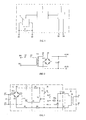
- FIG. 1 is a block diagram of a circuit configured to minimize standby power consumption in accordance with one embodiment of the present invention
- FIG. 2 is a schematic diagram of a conventional Power-frequency adapter
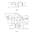
- FIG. 3 is a schematic diagram of the circuit shown in the FIG. 1 configured to minimize standby power consumption in accordance with one embodiment of the present invention
- FIG. 4 is a schematic diagram of a tri-voltage rectifying circuit applied in the present invention.
- FIG. 5 is a schematic diagram of the circuit shown in the FIG 3 coupled to the conventional Power-frequency adapter shown in the FIG. 2 .
- the block diagram as shown in FIG. 1 is a four-terminal network of which the input terminals are X3 and X4, while the output terminals are X1 and X2.
- the circuit configured to minimize standby power consumption in accordance with embodiments of the present invention comprises sensing circuitry 1, driving circuitry 2, switching circuitry 3 and a resistive element Z.
- terminals X1 and X2 disconnect the AC input on a primary side of a power-frequency transformer T1.
- Terminals X3 and X4 disconnect the AC output on the secondary side of the power-frequency transformer T1.
- the power-frequency transformer T1 is not interrupted by the circuit configured to minimize standby power consumption, so a power adapter using the power-frequency transformer T1 is still a conventional power-frequency adapter.
- the conventional power-frequency adapter generally comprises three parts, namely power-frequency transformer T1, bridge rectifier VC1 and filtering electrolytic capacitor C1.
- IN1 and IN2 are two terminals inputting power-frequency alternating current from the mains supply
- OUT1 and OUT2 are two terminals through which the power-frequency adapter outputs the low-voltage direct current.
- Sensing circuitry 1 has the functions of detecting and isolation sensing. Sensing circuitry 1 detects out whether there is a power supply signal indicative of powering the electrical appliances in work mode, isolates it and then sends a corresponding sensing signal to the subsequent circuits.
- the power supply signal is input by two input terminals X3 and X4 of the four-terminal network.
- the driving circuitry 2 has the functions of signal amplification and driving. The driving circuitry 2 amplifies the weak sensing signal from the sensing circuitry 1 and outputs a corresponding driving signal to control the switching on/off of the switching circuitry 3.
- the switching circuitry 3 When the power supply is in work mode, the switching circuitry 3 is switched on; otherwise it is switched off. Two connecting terminals of the switching circuitry 3 are X1 and X2, namely the output terminals X1 and X2 of the four-terminal network.
- the resistive element Z is coupled in parallel between terminals X1 and X2. If the four terminals X1, X2, X3 and X4 in FIG. 1 are respectively connected to the four terminals X1, X2, X3 and X4 in FIG. 2 , this becomes the design scheme for a "power-frequency adapter with ultra-low standby power consumption".
- the transmitted signal is AC signal
- X1 in FIG. 1 can also be connected with X2 in FIG. 2 ; X2 in FIG.
- the resistive element Z is coupled in parallel between terminals X1 and X2.
- the resistive element Z is coupled in parallel with the switching circuitry 3.
- the switching circuitry 3 When on standby, the switching circuitry 3 is switched off, and the resistive element Z serves as the AC route of the primary side of the power-frequency transformer T1.
- Select a suitable value for resistive element Z so as to make a very small current passing through the primary side of power-frequency transformer T1 when on standby.
- there is no current passing through the secondary side of the power-frequency transformer T1 but there is an induced voltage which is in direct proportion to the inductance of the primary side.
- the secondary side of the power-frequency transformer T1 At the time, if there is a load connected, the secondary side of the power-frequency transformer T1 has a small current which will be detected out by the sensing circuitry 1.
- the sensing circuitry 1 isolates it and sends a corresponding sensing signal to the driving circuitry 2.
- the driving circuitry 2 amplifies the sensing signal and then switches on the switching circuitry 3, so the resistive element Z is shorted, and the power-frequency adapter gains normal power supply.
- the resistive element Z can be a resistance, a capacitive reactance, a combination of resistance and capacitive reactance, or a constant current source formed by electronic components. For convenience, a high resistance or a low capacitance can be adopted for the resistive element Z.
- the Sensing circuitry 1 detects whether the load of the power-frequency transformer T1 is in work mode, and then sends a corresponding signal to the subsequent circuit.
- the Sensing circuitry 1 comprises a current transformer T2. As shown by dashed line box A of FIG. 3 , when in standby mode, there is no current on the secondary side of the power-frequency transformer T1, and the induced voltage of the secondary side of the current transformer T2 is zero. Once the load being started on by the power adapter, there is a small current passing through the secondary side of the power-frequency transformer T1, and the induced voltage of the secondary side of the current transformer T2 becomes above zero.
- the small current passing through the secondary side of power-frequency transformer T1 works as a power supply signal, and the current transformer T2 senses it and generates the induced voltage in the secondary side thereof as the sensing signal corresponding to the power supply signal.
- the magnetic materials with high magnetic permeability, as well as suitable ratio of primary to secondary coils will be selected therein.
- the current transformer T2 can also isolate the circuit from the power adapter when the power adapter is in normal work mode. In normal work mode, the current transformer T2 induces the small current of the power-frequency transformer T1 but doesn't influence it, so the power-frequency transformer T1 works independently in normal work mode.
- he sensing circuitry 1 is a kind of "electricity-to-magnetism-to-electricity" converter.
- circuits which can realize the conversion of "electricity-to-magnetism-to-electricity”.
- the Hall elements, magneto-dependent sensor (Wiegand device), electret elements and so forth once used suitably, also can realize the conversion of "electricity-to-magnetism-to- electricity”.
- Driving circuitry 2 is responsible for amplifying the weak sensing signal from the sensing circuitry 1, and controlling the switching on/off of the switching circuitry 3.
- capacitors C3 and C4 as well as diodes VD1 and VD2 form a double-voltage rectification circuit which not only performs the amplification but also generates a DC driving signal adapted for driving the switching circuitry 3. If the magnification factor of the double-voltage rectification circuit is not enough, the multi-voltage rectification circuit can be adopted, for instance, a tri-voltage rectification circuit as shown in FIG 4 .
- resistances R1, R2 and R3 as well as triodes V1 and V2 form an circuit with amplification and driving functions, which amplifies the DC driving signal of the double-voltage rectification circuit to gain a power enough to control the switching on/off of the switching circuitry 3.
- the circuit formed by the resistances R1, R2 and R3 as well as the triodes V1 and V2 is a kind of tri-pole transistor separating-element amplifier.
- the circuits in the dashed line box B are connected as follows: the capacitor C3 and the negative electrode of the diode VD1 are connected in series to a series connection point (3); the other terminal of the capacitor C3 is connected to an output terminal (1) of the current transformer T2; the positive electrode of the diode VD1 is connected to the other output terminal (2) of T2; the positive electrode of VD2 is connected to the series connection point (3) of the capacitor C3 and the diode VD1; the resistance R3 and the capacitor C4 are connected in series to a point (4) to which the negative electrode of the diode VD2 is connected; the other terminal of the resistance R3 is connected to the base electrode of the triode V1; the other terminal of the capacitor C4 is connected to the output terminal (2) of T2; the collector electrodes of the triodes V1 and V2 are connected with each other and then connected to the resistance R1; the other terminal of the resistance R1 is connected to a positive electrode (7) of a thyristor VT1; the emitter electrode of
- the switching circuitry 3 is shown in the dashed line box C of the FIG. 3 .
- the switching circuitry 3 When the load is connected with the power supply, the switching circuitry 3 shall be switched on, otherwise it shall be switched off.
- the switching circuitry 3 comprises the thyristor VT1 and a bridge rectifier VC2.
- the positive electrode (7) of the thyristor VT1 is connected to the positive output terminal (9) of the bridge rectifier VC2; the negative electrode (8) of the thyristor VT1 is connected to the negative output terminal (10) of the bridge rectifier VC2; the gate electrode (6) of the thyristor VT1 is connected to the emitter electrode of the triode V2; the AC input terminals (11) and (12) serve as the output terminals X1 and X2 of the four-terminal network.
- the resistive element Z is a capacitance C2 connected between X1 and X2.
- the thyristor VT1 is a "semi-controlled” element which can be replaced by "all-controlled” elements such as crystal triode, field effect transistor, IGBT transistor, etc.
- the emitter electrode of the triode V2 When the load is connected with the power supply, the emitter electrode of the triode V2 outputs the current to trigger the gate electrode of the thyristor VT1, and the thyristor VT1 switches into conduction. Then, X1 and X2 are disconnected through the diodes in the bridge rectifier VC2, thus the resistive element Z is shorted, and the power-frequency adapter gets normal power supply.
- circuits which can be used for amplification, driving and switching, so the circuits shall be selected according to the cost, technical situation and the possibility of volume miniaturization.
- the circuit minimizing standby power in a power supply system in accordance with embodiments of the present invention is a four-terminal network, of which the input terminals are X3 and X4, and the output terminals are X1 and X2; the input terminals X3 and X4 are connected in series to the secondary side of the power-frequency transformer T1 of the power adapter, while the output terminals X1 and X2 are connected in series to the primary side of the power-frequency transformer T1; the four-terminal network comprises sensing circuitry, driving circuitry, switching circuitry and a resistive element.
- the first part of the four-terminal network is used as the detecting and isolation sensing part, which, in fact, is an "electricity-to-magnetism-to-electricity" converter.
- the current transformer shall be a preferred selection for the "electricity-to-magnetism-to-electricity” converter.
- the Hall elements, magneto-dependent sensor (Wiegand device), electret elements also can be adopted for this part.
- the second part of the four-terminal network is used as the signal amplification and driving part.
- Double-voltage rectifying or multi-voltage rectifying circuits are preferred selection for amplifying a sensing signal from the first part of the circuit; and tri-pole transistor separating-element amplifier is a preferred selection as the driving part.
- the third part of the four-terminal network is an electronic switch and a resistive element.
- the resistive element shall be connected to the two output terminals X1 and X2 of the four-terminal network, and in parallel connection with the electronic switch.
- a thyristor and a bridge rectifier are preferred selection to form the electronic switch.
- the electronic switch when the detecting and isolation sensing part senses a power supply signal of the power adapter in work mode, the electronic switch shorts the resistive element; and when the power adapter is in standby mode, the electronic switch is switched off and the resistive element is coupled to the power adapter.
- FIG. 5 shows the overall circuit diagram of this kind of power-frequency adapter, which is composed of circuits in FIG. 2 and FIG. 3 .
Landscapes
- Business, Economics & Management (AREA)
- Emergency Management (AREA)
- Engineering & Computer Science (AREA)
- Power Engineering (AREA)
- Rectifiers (AREA)
- Dc-Dc Converters (AREA)
Applications Claiming Priority (2)
| Application Number | Priority Date | Filing Date | Title |
|---|---|---|---|
| CNU2006200148512U CN200976549Y (zh) | 2006-09-22 | 2006-09-22 | 一种超低功耗待机电路 |
| PCT/CN2007/002210 WO2008037167A1 (fr) | 2006-09-22 | 2007-07-20 | Circuit de secours à consommation électrique super faible |
Publications (1)
| Publication Number | Publication Date |
|---|---|
| EP2068432A1 true EP2068432A1 (fr) | 2009-06-10 |
Family
ID=38902828
Family Applications (1)
| Application Number | Title | Priority Date | Filing Date |
|---|---|---|---|
| EP07785143A Withdrawn EP2068432A1 (fr) | 2006-09-22 | 2007-07-20 | Circuit de secours à consommation électrique super faible |
Country Status (4)
| Country | Link |
|---|---|
| US (1) | US8125804B2 (fr) |
| EP (1) | EP2068432A1 (fr) |
| CN (1) | CN200976549Y (fr) |
| WO (1) | WO2008037167A1 (fr) |
Cited By (1)
| Publication number | Priority date | Publication date | Assignee | Title |
|---|---|---|---|---|
| EP2405304A3 (fr) * | 2010-07-05 | 2016-04-06 | Samsung Electronics Co., Ltd. | Alimentation électrique de mode de commutation et procédé d'alimentation électrique l'utilisant |
Families Citing this family (11)
| Publication number | Priority date | Publication date | Assignee | Title |
|---|---|---|---|---|
| KR100923220B1 (ko) * | 2008-06-04 | 2009-10-27 | (주)골든칩스 | 스위칭 모드 전원 공급기의 대기전력 최소화장치 |
| US20120146402A1 (en) * | 2010-12-09 | 2012-06-14 | Siemens Industry, Inc. | Control system for regulating bus voltage for an electric shovel |
| FR2969864A1 (fr) * | 2010-12-23 | 2012-06-29 | St Microelectronics Tours Sas | Circuit d'alimentation a faibles pertes en mode veille |
| KR101199199B1 (ko) * | 2010-12-27 | 2012-11-07 | 엘지이노텍 주식회사 | 전원 공급 장치 |
| JP5929667B2 (ja) * | 2012-09-25 | 2016-06-08 | 富士ゼロックス株式会社 | 画像形成装置及びバイアス電源装置 |
| CN202995349U (zh) * | 2012-12-26 | 2013-06-12 | 黄冠雄 | 微功耗待机系统及厚膜混合集成电路模块 |
| US20170324270A1 (en) * | 2013-12-26 | 2017-11-09 | Calvin Shie-Ning Wang | Standby circuit, and outlet, plug, and device having the same |
| CN106209050B (zh) * | 2016-08-19 | 2023-08-04 | 德力西电气有限公司 | 一种低成本低功耗的电子开关电路 |
| CN108063559B (zh) * | 2017-11-20 | 2020-07-07 | 中山市尊宝实业有限公司 | 一种待机状态超低功耗电源 |
| US11277024B2 (en) | 2020-07-24 | 2022-03-15 | ZQ Power, LLC | Devices, systems, and methods for reducing standby power consumption |
| CN112350621A (zh) * | 2020-10-29 | 2021-02-09 | 南京理工大学 | 一种应用于无刷电机的驱动电路 |
Family Cites Families (17)
| Publication number | Priority date | Publication date | Assignee | Title |
|---|---|---|---|---|
| US4016458A (en) * | 1975-01-23 | 1977-04-05 | Jerrold Electronics Corporation | Radio frequency distribution network standby power system with overvoltage protection |
| KR920000347Y1 (ko) * | 1989-12-29 | 1992-01-15 | 삼성전자 주식회사 | 두 출력의 smps 콘트롤 회로 |
| JPH06292363A (ja) * | 1993-04-05 | 1994-10-18 | Fuji Facom Corp | Acアダプタ |
| GB9623612D0 (en) * | 1996-11-13 | 1997-01-08 | Rca Thomson Licensing Corp | Separate power supplies for standby operation |
| DE69826172T2 (de) * | 1997-04-30 | 2005-02-03 | Fidelix Y.K., Kiyose | Stromversorgungsgerät |
| JP2000004547A (ja) * | 1998-03-19 | 2000-01-07 | Kazuya Maeda | 電源回路およびacアダプタ |
| US6172492B1 (en) * | 1999-03-26 | 2001-01-09 | Sarnoff Corporation | Fixed off time and zero voltage switching dual mode power factor correcting converter |
| US6538419B1 (en) * | 2000-01-11 | 2003-03-25 | Thomson Licensing S.A. | Power supply with synchronized power on transition |
| US6324082B1 (en) * | 2000-06-06 | 2001-11-27 | Thomson Licensing, S.A. | Mains frequency synchronous burst mode power supply |
| JP2003111418A (ja) * | 2001-09-26 | 2003-04-11 | Sony Corp | 電源回路及びacアダプタ |
| JP2003299355A (ja) * | 2002-04-03 | 2003-10-17 | Seiko Epson Corp | Acアダプタ及び充電器 |
| JP4214484B2 (ja) * | 2002-12-12 | 2009-01-28 | サンケン電気株式会社 | 直流電源装置 |
| GB2420666B (en) * | 2003-08-08 | 2007-01-03 | Astec Int Ltd | A circuit for maintaining hold-up time while reducing bulk capacitor size and improving efficiency in a power supply |
| JP4127399B2 (ja) * | 2004-03-31 | 2008-07-30 | 松下電器産業株式会社 | スイッチング電源制御用半導体装置 |
| BRPI0510845A (pt) * | 2004-05-24 | 2007-11-27 | Young-Chang Cho | método de controle de baixa tensão usando uma forma de onda de energia de corrente alternada e sistema para controle de baixa tensão |
| JP4861981B2 (ja) * | 2004-07-23 | 2012-01-25 | トムソン ライセンシング | 待機電力消費を低減するためのシステム及び方法 |
| JP4099593B2 (ja) * | 2004-09-17 | 2008-06-11 | ソニー株式会社 | スイッチング電源回路 |
-
2006
- 2006-09-22 CN CNU2006200148512U patent/CN200976549Y/zh not_active Expired - Fee Related
-
2007
- 2007-07-20 WO PCT/CN2007/002210 patent/WO2008037167A1/fr active Application Filing
- 2007-07-20 EP EP07785143A patent/EP2068432A1/fr not_active Withdrawn
- 2007-07-20 US US12/306,580 patent/US8125804B2/en not_active Expired - Fee Related
Non-Patent Citations (1)
| Title |
|---|
| See references of WO2008037167A1 * |
Cited By (1)
| Publication number | Priority date | Publication date | Assignee | Title |
|---|---|---|---|---|
| EP2405304A3 (fr) * | 2010-07-05 | 2016-04-06 | Samsung Electronics Co., Ltd. | Alimentation électrique de mode de commutation et procédé d'alimentation électrique l'utilisant |
Also Published As
| Publication number | Publication date |
|---|---|
| WO2008037167A1 (fr) | 2008-04-03 |
| US20090185402A1 (en) | 2009-07-23 |
| CN200976549Y (zh) | 2007-11-14 |
| US8125804B2 (en) | 2012-02-28 |
Similar Documents
| Publication | Publication Date | Title |
|---|---|---|
| US8125804B2 (en) | Circuit for minimizing standby power in power supply systems | |
| TWI414119B (zh) | 電源供應器以及具有複數個電源供應器之供電系統 | |
| CN1518200B (zh) | 开关式电源装置 | |
| US10862400B2 (en) | Resonant power converter and switching method | |
| CN104578844A (zh) | 一种开关电源电路 | |
| CN100436022C (zh) | 具有高功率因子的电弧焊机发电机 | |
| CN102694477B (zh) | 高压交流与低压交流和低压直流三电源共地的电路 | |
| CN103973138A (zh) | 动态变频电源转换系统 | |
| TW201433058A (zh) | 動態變頻電源轉換系統 | |
| CN204733079U (zh) | 一种功放供电电路及tv电源板 | |
| CN101149596A (zh) | 一种超低功耗待机电路 | |
| CN101707392B (zh) | 不间断电源的交直流隔离控制方法及电路 | |
| CN105281577A (zh) | 一种功放供电电路及tv电源板 | |
| CN202837873U (zh) | 零功率待机电路及相应电子产品 | |
| CN202663316U (zh) | 高压交流与低压交流和低压直流三电源共地的电路 | |
| CN202256445U (zh) | 电压检测电路 | |
| US10014796B2 (en) | Power transformer | |
| CN205544951U (zh) | 一种低空载损耗的变压器系统 | |
| CN220457290U (zh) | 功率因数校正器、功率因数校正电路和电源设备 | |
| CN109586397A (zh) | 电源控制电路及电子设备 | |
| CN220359032U (zh) | 功率因数校正器、功率因数校正电路和电源装备 | |
| CN220382954U (zh) | 一种高效的开关电源电路 | |
| CN210137282U (zh) | 全桥式谐振转换电路 | |
| CN213585578U (zh) | 一种同步转换器控制电路 | |
| CN211579862U (zh) | 一种反激电源输入电流补偿电路 |
Legal Events
| Date | Code | Title | Description |
|---|---|---|---|
| PUAI | Public reference made under article 153(3) epc to a published international application that has entered the european phase |
Free format text: ORIGINAL CODE: 0009012 |
|
| 17P | Request for examination filed |
Effective date: 20090422 |
|
| AK | Designated contracting states |
Kind code of ref document: A1 Designated state(s): AT BE BG CH CY CZ DE DK EE ES FI FR GB GR HU IE IS IT LI LT LU LV MC MT NL PL PT RO SE SI SK TR |
|
| AX | Request for extension of the european patent |
Extension state: AL BA HR MK RS |
|
| DAX | Request for extension of the european patent (deleted) | ||
| STAA | Information on the status of an ep patent application or granted ep patent |
Free format text: STATUS: THE APPLICATION IS DEEMED TO BE WITHDRAWN |
|
| 18D | Application deemed to be withdrawn |
Effective date: 20130201 |