EP2068245A2 - Verlässlichkeits-, Zuverlässigkeits- und Dienstbarkeitslösungen für die Speichertechnologie - Google Patents
Verlässlichkeits-, Zuverlässigkeits- und Dienstbarkeitslösungen für die Speichertechnologie Download PDFInfo
- Publication number
- EP2068245A2 EP2068245A2 EP08169196A EP08169196A EP2068245A2 EP 2068245 A2 EP2068245 A2 EP 2068245A2 EP 08169196 A EP08169196 A EP 08169196A EP 08169196 A EP08169196 A EP 08169196A EP 2068245 A2 EP2068245 A2 EP 2068245A2
- Authority
- EP
- European Patent Office
- Prior art keywords
- crc
- logic
- read
- write
- bits
- Prior art date
- Legal status (The legal status is an assumption and is not a legal conclusion. Google has not performed a legal analysis and makes no representation as to the accuracy of the status listed.)
- Granted
Links
- 238000005516 engineering process Methods 0.000 title abstract description 6
- 238000000034 method Methods 0.000 claims abstract description 13
- 125000004122 cyclic group Chemical group 0.000 claims abstract description 8
- 238000001514 detection method Methods 0.000 claims 3
- 230000009977 dual effect Effects 0.000 claims 2
- 238000010586 diagram Methods 0.000 description 16
- 238000009432 framing Methods 0.000 description 4
- 230000003287 optical effect Effects 0.000 description 2
- 230000005540 biological transmission Effects 0.000 description 1
- 238000004891 communication Methods 0.000 description 1
- 238000004590 computer program Methods 0.000 description 1
- 230000006870 function Effects 0.000 description 1
- 230000007257 malfunction Effects 0.000 description 1
- 230000001052 transient effect Effects 0.000 description 1
Images


Classifications
-
- G—PHYSICS
- G06—COMPUTING; CALCULATING OR COUNTING
- G06F—ELECTRIC DIGITAL DATA PROCESSING
- G06F11/00—Error detection; Error correction; Monitoring
- G06F11/07—Responding to the occurrence of a fault, e.g. fault tolerance
- G06F11/08—Error detection or correction by redundancy in data representation, e.g. by using checking codes
- G06F11/10—Adding special bits or symbols to the coded information, e.g. parity check, casting out 9's or 11's
- G06F11/1004—Adding special bits or symbols to the coded information, e.g. parity check, casting out 9's or 11's to protect a block of data words, e.g. CRC or checksum
-
- G—PHYSICS
- G06—COMPUTING; CALCULATING OR COUNTING
- G06F—ELECTRIC DIGITAL DATA PROCESSING
- G06F11/00—Error detection; Error correction; Monitoring
- G06F11/07—Responding to the occurrence of a fault, e.g. fault tolerance
- G06F11/08—Error detection or correction by redundancy in data representation, e.g. by using checking codes
- G06F11/10—Adding special bits or symbols to the coded information, e.g. parity check, casting out 9's or 11's
-
- G—PHYSICS
- G06—COMPUTING; CALCULATING OR COUNTING
- G06F—ELECTRIC DIGITAL DATA PROCESSING
- G06F12/00—Accessing, addressing or allocating within memory systems or architectures
Definitions
- Embodiments of the invention generally relate to the field of information technology and, more particularly, to systems, methods and apparatuses for reliability, availability, and serviceability solutions for memory technology.
- ECCs error correcting codes
- FIG. 1 is a block diagram illustrating selected aspects of a write cyclic redundancy code (CRC) scheme, according to an embodiment of the invention.
- CRC write cyclic redundancy code
- Figure 2 is a block diagram illustrating selected aspects of a read CRC scheme, according to an embodiment of the invention.
- FIG. 3 is a block diagram illustrating selected aspects of a CRC scheme in a memory subsystem including a registered dual-inline memory module (RDIMM), according to an embodiment of the invention.
- RDIMM registered dual-inline memory module
- FIG. 4 is a block diagram illustrating selected aspects of a CRC scheme in a memory subsystem including an unregistered dual-inline memory module (UDIMM), according to an embodiment of the invention.
- UMIMM unregistered dual-inline memory module
- FIG. 5 is a block diagram illustrating selected aspects of frame formats for x4 and x8 dynamic random access memory devices (DRAMs), according to an embodiment of the invention.
- DRAMs dynamic random access memory devices
- Figure 6 is a block diagram illustrating selected aspects of a frame format for a x16 DRAM, according to an embodiment of the invention.
- Figure 7 is a block diagram illustrating selected aspects of offsetting the CRC bits from the data bits, according to an embodiment of the invention.
- Figure 8 is a flow diagram illustrating selected aspects of a method for providing CRC in different market segments without substantially changing the form factors of the components in the memory subsystems.
- Embodiments of the invention are generally directed to systems, methods, and apparatuses for providing RAS (reliability, availability, and serviceability) solutions within a certain set of volumetric constraints.
- a computing system uses different cyclic redundancy code (CRC) schemes for write CRC coverage (or simply write CRC) and read CRC coverage (or simply read CRC).
- CRC schemes may be provided while maintaining the same DRAM (dynamic random access memory) form factors that are currently used in the server and client market segments.
- CRC coverage is provided for read and/or write data without adding additional pins to the connector. As is further discussed below, this may be achieved by adding user intervals (UIs) to the data frames and/or multiplexing CRC bits over existing pins.
- UIs user intervals
- FIG. 1 is a block diagram illustrating selected aspects of a write CRC scheme, according to an embodiment of the invention.
- system 100 includes host 110 (e.g., a memory controller), connector 120, memory module 130, and memory device (e.g., a DRAM) 140.
- host 110 e.g., a memory controller
- connector 120 e.g., a DRAM
- memory module 130 e.g., a DRAM
- FIG. 1 only shows a single connector 120, memory module 130, and memory device 140. It is to be appreciated, however, that each module 130 may include a number of memory devices 140 (e.g., 9, 18, ..., etc.).
- system 100 may include multiple connectors, modules, and the like. In alternative embodiments, system 100 may include more elements, fewer elements, and/or different elements.
- Host 110 controls the transfer of data to and from memory device 140.
- host 110 is integrated onto the same die as one or more processors.
- Host 110 includes CRC decision logic 112 and write CRC logic 114.
- CRC decision logic 112 determines the write CRC and read CRC schemes for system 100 during, for example, initialization.
- CRC decision logic 112 may read a non-volatile memory (such as a basic input/output (BIOS) and/or serial presence detect (SPD)) to determine the configuration of system 100.
- CRC decision logic 112 may then select a write CRC and/or a read CRC based at least in part on the configuration of system 100.
- BIOS basic input/output
- SPD serial presence detect
- module 130 is a registered dual-inline memory module (RDIMM)
- CRC decision logic 112 may select a write CRC and/or read CRC that is appropriate for an RDIMM configuration.
- module 130 is an unregistered dual-inline memory module (UDIMM)
- CRC decision logic 112 may select a write CRC and/or read CRC that is appropriate for a UDIMM configuration.
- the same connector 120 may be used for a number of different system configurations (e.g., RDIMM, UDIMM, and the like).
- connector 120 may have the same form factor that was developed for previous generations of memory technology (e.g., connector 120 may be approximately 5.25 inches in length).
- write CRC logic 114 includes CRC generation logic and/or framing logic.
- the CRC generation logic generates a CRC that memory device 140 can compare with a locally generated checksum to determine whether write data includes an error.
- the framing logic enables host 110 to operate in a mode in which M UIs of CRC bits (106) are added to N UIs of write data (108) in a write data frame.
- M is two and N is eight. In alternative embodiments, M and/or N may have different values.
- write CRC logic 114 may support more than one write CRC scheme.
- write CRC logic 114 may support multiplexing write CRC bits over a preexisting pin (such as a data strobe pin).
- preexisting pin refers to a pin that is specified by a previous generation of double data rate (DDR) memory technology that did not support CRC.
- DDR double data rate
- preexisting pin also refers to a pin that is used by a system in RDIMM mode and that is not needed in UDIMM mode.
- CRC decision logic 112 and write CRC logic 114 are each illustrated as a single block of logic. It is to be appreciated, however, that logic 112 and/or logic 114 may be subsumed into other blocks of logic and/or may be divided into a number of other blocks of logic.
- Command/Address (C/A) lanes 102 provide a plurality of lanes for sending commands and addresses to memory device 140.
- DQ lanes 104 provide a bi-directional read/write data bus.
- Embodiments of the invention may be used with memory devices of nearly any data width including: x4, x8, x16, x32, and the like.
- Memory device 140 includes memory core 142 (e.g., a memory array) and write CRC logic 144.
- Write CRC logic 144 includes logic to enable memory device 140 to support one or more write CRC schemes.
- write CRC logic 144 include logic to separate the M UIs of write CRC bits from the N UIs of data bits in a write data frame.
- Write CRC logic 144 may also include a local CRC generator and comparison logic to compare the received write CRC bits with a locally generated checksum.
- write CRC logic 144 may support more than one write CRC scheme. For example, in addition to the scheme described above, write CRC logic 144 may support de-multiplexing write CRC bits over a preexisting pin (such as a data strobe pin). In other embodiments, write CRC logic 144 may support other write CRC schemes.
- FIG. 2 is a block diagram illustrating selected aspects of a read CRC scheme, according to an embodiment of the invention.
- System 200 includes host 110 (e.g., a memory controller), connector 120, memory module 130, and memory device (e.g., a DRAM) 140.
- host 110 e.g., a memory controller
- connector 120 e.g., a memory module
- memory device 140 e.g., a DRAM
- system 200 may include more elements, fewer elements, and/or different elements.
- Host 110 includes read CRC logic 216 to support one or more read CRC schemes.
- Read CRC logic 216 may include error correction code (ECC) logic to provide ECC coverage for data bits written to memory device 140 (e.g., to protect against soft errors).
- ECC error correction code
- host 110 and memory device 140 disable their CRC capabilities (e.g., using enable/disable logic 246) during read operations and rely on the ECC logic to cover read data. If the ECC logic indicates an error, then (in some embodiments) the read operation may be replayed. If an error persists, then the ECC logic may attempt to correct it.
- read CRC logic 216 supports more than one read CRC scheme.
- read CRC logic 216 may support de-multiplexing read CRC bits over a preexisting pin (such as a data strobe pin).
- read CRC logic 216 may support other read CRC schemes.
- memory device 140 includes read CRC logic 248 to support one or more read CRC schemes.
- Read CRC logic 248 may include a CRC generator to generate a checksum (e.g., CRC bits) to cover read data that is being returned to host 110.
- read CRC logic 248 may include logic to multiplex the CRC bits over a preexisting pin (e.g., a data strobe pin such as pin 250).
- pin broadly refers to any electrical contact suitable for conducting electrical signals (such as a pad, ball, pin, and the like).
- read CRC logic 248 may include logic to add M UIs of CRC bits to N UIs of data bits to form a read data frame.
- read CRC logic 248 may support other read CRC schemes.
- FIG. 3 is a block diagram illustrating selected aspects of a CRC scheme in a memory subsystem including a registered dual-inline memory module (RDIMM), according to an embodiment of the invention.
- System 300 includes host 110 (e.g., a memory controller) and RDIMM 320. In alternative embodiments, system 300 may include more elements, fewer elements, and/or different elements. In some embodiments, system 300 is a server.
- RDIMM 320 includes a number (e.g., 9, 18, etc.) of DRAMs 322 and register (or buffer) 324. One or more of DRAMs 322 store ECC bits generated by logic 216 on host 110. In some embodiments, RDIMM 320 may include more elements, fewer elements, and/or different elements.
- CRC decision logic 112 may access non-volatile memory (e.g., SPD 326) to determine, at least in part, the configuration of system 300.
- CRC decision logic 112 may select a read CRC scheme and a write CRC scheme after determining the configuration of system 300.
- CRC decision logic 112 determines that host 110 is coupled with RDIMM 320 (and may be configured as a server).
- Decision logic 112 selects a write CRC scheme that includes framing M UIs of CRC bits (106) with N UIs of data bits to form a write data frame.
- DRAMs 322 may include corresponding logic to separate the M UIs of CRC bits and compare them with a locally generated checksum.
- Decision logic 112 may also select a read CRC scheme.
- decision logic 112 since host 110 includes support for ECC, decision logic 112 may select a scheme in which the ECC bits are relied upon to provide error coverage in the read direction.
- decision logic 112 may select a different read CRC scheme and/or a different write CRC scheme.
- the read CRC scheme may include adding M UIs of CRC bits to the read data frame.
- FIG. 4 is a block diagram illustrating selected aspects of a CRC scheme in a memory subsystem including an unregistered dual-inline memory module (UDIMM), according to an embodiment of the invention.
- System 400 includes host 110 (e.g., a memory controller) and UDIMM 420.
- host 110 e.g., a memory controller
- UDIMM 420 e.g., a memory controller
- system 400 may include more elements, fewer elements, and/or different elements.
- system 400 is a client system.
- UDIMM 420 includes a number (e.g., 9, 18, etc.) of DRAMs 422 and SPD 426. In alternative embodiments, UDIMM 420 may include more elements, fewer elements, and/or different elements.
- CRC decision logic 112 may access non-volatile memory (e.g., SPD 426) to determine, at least in part, the configuration of system 400.
- CRC decision logic 112 may select a read CRC scheme and a write CRC scheme after determining the configuration of system 400.
- CRC decision logic 112 determines that host 110 is coupled with UDIMM 420 (and may be configured as a client).
- Decision logic 112 selects a write CRC scheme that includes framing M UIs of CRC bits (106) with N UIs of data bits (108) to form a write data frame.
- DRAMs 422 may include corresponding logic to separate the M UIs of CRC bits and compare them with a locally generated checksum.
- Decision logic 112 may also select a read CRC scheme.
- the read CRC scheme includes multiplexing the CRC bits over one or more preexisting pins (e.g., pin 250 shown in FIG. 2 ).
- the preexisting pins are data strobe pins such as the TDQS/TDQS# pins.
- the CRC bits may be multiplexed over a different pin or pins.
- DRAMs 422 may include logic to multiplex the CRC bits on the pin(s) and host 110 may include logic to de-multiplex the CRC bits from the pin(s).
- decision logic 112 may select a different read CRC scheme and/or a different write CRC scheme.
- the read CRC scheme may include adding M UIs of CRC bits to the read data frame.
- system 400 may support ECC coverage and the read CRC scheme may rely on the ECC coverage.
- FIG. 5 is a block diagram illustrating selected aspects of frame formats for x4 and x8 dynamic random access memory devices (DRAMs), according to an embodiment of the invention.
- Frame 510 illustrates the frame format for an embodiment of the invention in which two UIs of CRC bits are combined with eight UIs of data bits for a x4 device.
- frame 520 illustrates the frame format for an embodiment of the invention in which two UIs of CRC bits are combined with eight UIs of data bits for a x8 device.
- a different number of UIs may be used for the CRC bits and/or the data bits.
- FIG. 6 is a block diagram illustrating selected aspects of a frame format in a x16 DRAM, according to an embodiment of the invention.
- Frame 600 illustrates the frame format for an embodiment of the invention in which two UIs of CRC bits are combined with eight UIs of data bits for a x16 device.
- the x16 device frame format is essentially two instances of the x8 frame format (e.g., frame 520 shown in FIG. 5 ).
- FIG. 7 is a block diagram illustrating selected aspects of offsetting the CRC bits from the data bits, according to an embodiment of the invention.
- the CRC bits are offset from the data bits to improve latency. For example, transmission of the data bits may begin before the corresponding CRC bits are generated.
- the offset between the data bits is 1 ⁇ 2 of a frame as shown by 710 (for a x4 device) and 720 (for a x8 device). In alternative embodiments, the offset may be different (or may not be used at all).
- Other frame formats for arranging data bits and CRC bits that are suitable for use with separate CRC pins may be used in other embodiments of the invention..
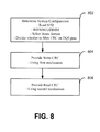
- FIG. 8 is a flow diagram illustrating selected aspects of a method for providing CRC in different market segments without substantially changing the form factors of the components in the memory subsystems.
- CRC decision logic e.g., 112, in FIG. 1 determines the configuration of a system. This process may include accessing information about the elements in the system and the manner in which the elements are interconnected. In some embodiments, the decision logic determines whether a host is connected to an RDIMM or a UDIMM.
- the decision logic selects a read CRC scheme and a write CRC scheme based, at least in part, on the configuration of the system. Selecting the CRC schemes may include selecting a frame format for the write direction and/or the read direction. It may also (or alternatively) include deciding whether to multiplex/de-multiplex the CRC bits on one or more preexisting pins (e.g., data strobe pins).
- the host provides a write CRC scheme.
- the write CRC scheme includes adding M UIs of CRC bits to N UIs of data bits to create a write data frame.
- the write CRC scheme includes multiplexing/de-multiplexing the CRC bits on a preexisting pin(s).
- the host provides a read CRC scheme.
- the read CRC scheme includes relying on ECC logic to provide coverage of the read data bits.
- it includes adding M UIs of CRC bits to N UIs of data bits to create a read data frame.
- the read CRC scheme may include multiplexing/de-multiplexing the CRC bits on a preexisting pin(s).
- Elements of embodiments of the present invention may also be provided as a machine-readable medium for storing the machine-executable instructions.
- the machine-readable medium may include, but is not limited to, flash memory, optical disks, compact disks-read only memory (CD-ROM), digital versatile/video disks (DVD) ROM, random access memory (RAM), erasable programmable read-only memory (EPROM), electrically erasable programmable read-only memory (EEPROM), magnetic or optical cards, propagation media or other type of machine-readable media suitable for storing electronic instructions.
- embodiments of the invention may be downloaded as a computer program which may be transferred from a remote computer (e.g., a server) to a requesting computer (e.g., a client) by way of data signals embodied in a carrier wave or other propagation medium via a communication link (e.g., a modem or network connection).
- a remote computer e.g., a server
- a requesting computer e.g., a client
- a communication link e.g., a modem or network connection
- logic is representative of hardware, firmware, software (or any combination thereof) to perform one or more functions.
- examples of “hardware” include, but are not limited to, an integrated circuit, a finite state machine, or even combinatorial logic.
- the integrated circuit may take the form of a processor such as a microprocessor, an application specific integrated circuit, a digital signal processor, a micro-controller, or the like.
Landscapes
- Engineering & Computer Science (AREA)
- Theoretical Computer Science (AREA)
- General Engineering & Computer Science (AREA)
- Physics & Mathematics (AREA)
- General Physics & Mathematics (AREA)
- Quality & Reliability (AREA)
- Computer Security & Cryptography (AREA)
- Techniques For Improving Reliability Of Storages (AREA)
- Hardware Redundancy (AREA)
Applications Claiming Priority (1)
| Application Number | Priority Date | Filing Date | Title |
|---|---|---|---|
| US11/942,621 US8132074B2 (en) | 2007-11-19 | 2007-11-19 | Reliability, availability, and serviceability solutions for memory technology |
Publications (3)
| Publication Number | Publication Date |
|---|---|
| EP2068245A2 true EP2068245A2 (de) | 2009-06-10 |
| EP2068245A3 EP2068245A3 (de) | 2009-07-22 |
| EP2068245B1 EP2068245B1 (de) | 2011-03-16 |
Family
ID=40409870
Family Applications (1)
| Application Number | Title | Priority Date | Filing Date |
|---|---|---|---|
| EP08169196A Active EP2068245B1 (de) | 2007-11-19 | 2008-11-14 | Verlässlichkeits-, Zuverlässigkeits- und Dienstbarkeitslösungen für die Speichertechnologie |
Country Status (6)
| Country | Link |
|---|---|
| US (2) | US8132074B2 (de) |
| EP (1) | EP2068245B1 (de) |
| KR (1) | KR101031436B1 (de) |
| CN (1) | CN101441896B (de) |
| AT (1) | ATE502333T1 (de) |
| DE (1) | DE602008005541D1 (de) |
Cited By (4)
| Publication number | Priority date | Publication date | Assignee | Title |
|---|---|---|---|---|
| GB2494237A (en) * | 2011-09-01 | 2013-03-06 | Ibm | Data verification using checksum sidefile |
| EP2727115A2 (de) * | 2011-07-01 | 2014-05-07 | Intel Corporation | Rangspezifische zyklische redundanzprüfung |
| WO2015105948A1 (en) * | 2014-01-09 | 2015-07-16 | Qualcomm Incorporated | Dynamic random access memory (dram) backchannel communication systems and methods |
| WO2021041023A1 (en) * | 2019-08-30 | 2021-03-04 | Qualcomm Incorporated | Memory with system ecc |
Families Citing this family (12)
| Publication number | Priority date | Publication date | Assignee | Title |
|---|---|---|---|---|
| US8279948B2 (en) * | 2006-12-13 | 2012-10-02 | Rambus Inc. | Interface with variable data rate |
| KR100951567B1 (ko) * | 2008-02-29 | 2010-04-09 | 주식회사 하이닉스반도체 | 데이터 전달의 신뢰성을 보장하기 위한 반도체 메모리 장치 |
| KR100929835B1 (ko) * | 2008-02-29 | 2009-12-07 | 주식회사 하이닉스반도체 | 안정적인 초기 동작을 수행하는 반도체 메모리 장치 |
| KR20110100465A (ko) | 2010-03-04 | 2011-09-14 | 삼성전자주식회사 | 메모리 시스템 |
| US8639964B2 (en) * | 2010-03-17 | 2014-01-28 | Dell Products L.P. | Systems and methods for improving reliability and availability of an information handling system |
| US8738993B2 (en) | 2010-12-06 | 2014-05-27 | Intel Corporation | Memory device on the fly CRC mode |
| CN102571478B (zh) * | 2010-12-31 | 2016-05-25 | 上海宽惠网络科技有限公司 | 服务器 |
| KR101700492B1 (ko) * | 2012-03-26 | 2017-01-26 | 인텔 코포레이션 | 에러 검출 코딩된 트랜잭션들을 이용한 메모리 디바이스들에 대한 타이밍 최적화 |
| KR101984902B1 (ko) | 2012-09-14 | 2019-05-31 | 삼성전자 주식회사 | 단방향의 리턴 클락 신호를 사용하는 임베디드 멀티미디어 카드, 이를 제어하는 호스트, 및 이들을 포함하는 임베디드 멀티미디어 카드 시스템의 동작 방법 |
| US9299400B2 (en) | 2012-09-28 | 2016-03-29 | Intel Corporation | Distributed row hammer tracking |
| US11061431B2 (en) * | 2018-06-28 | 2021-07-13 | Micron Technology, Inc. | Data strobe multiplexer |
| US10546620B2 (en) * | 2018-06-28 | 2020-01-28 | Micron Technology, Inc. | Data strobe calibration |
Citations (3)
| Publication number | Priority date | Publication date | Assignee | Title |
|---|---|---|---|---|
| US6519733B1 (en) | 2000-02-23 | 2003-02-11 | International Business Machines Corporation | Method and apparatus for high integrity hardware memory compression |
| WO2007100694A2 (en) | 2006-02-27 | 2007-09-07 | Intel Corporation | Systems, methods, and apparatuses for using the same memory type to support an error check mode and a non-error check mode |
| US20070226588A1 (en) | 2005-10-24 | 2007-09-27 | Lee Shea-Yun | Memory Device and Bit Error Detection Method Thereof |
Family Cites Families (8)
| Publication number | Priority date | Publication date | Assignee | Title |
|---|---|---|---|---|
| US6901551B1 (en) | 2001-12-17 | 2005-05-31 | Lsi Logic Corporation | Method and apparatus for protection of data utilizing CRC |
| US20060077750A1 (en) * | 2004-10-07 | 2006-04-13 | Dell Products L.P. | System and method for error detection in a redundant memory system |
| US7734980B2 (en) * | 2005-06-24 | 2010-06-08 | Intel Corporation | Mitigating silent data corruption in a buffered memory module architecture |
| US7380197B1 (en) * | 2005-07-12 | 2008-05-27 | Xilinx, Inc. | Circuit and method for error detection |
| US7587643B1 (en) * | 2005-08-25 | 2009-09-08 | T-Ram Semiconductor, Inc. | System and method of integrated circuit testing |
| US7844888B2 (en) * | 2006-09-29 | 2010-11-30 | Qimonda Ag | Electronic device, method for operating an electronic device, memory circuit and method of operating a memory circuit |
| US7861140B2 (en) * | 2006-10-31 | 2010-12-28 | Globalfoundries Inc. | Memory system including asymmetric high-speed differential memory interconnect |
| KR101308047B1 (ko) * | 2007-02-08 | 2013-09-12 | 삼성전자주식회사 | 메모리 시스템, 이 시스템을 위한 메모리, 및 이 메모리를위한 명령 디코딩 방법 |
-
2007
- 2007-11-19 US US11/942,621 patent/US8132074B2/en active Active
-
2008
- 2008-11-14 DE DE602008005541T patent/DE602008005541D1/de active Active
- 2008-11-14 EP EP08169196A patent/EP2068245B1/de active Active
- 2008-11-14 AT AT08169196T patent/ATE502333T1/de not_active IP Right Cessation
- 2008-11-19 CN CN2008101815324A patent/CN101441896B/zh active Active
- 2008-11-19 KR KR1020080115184A patent/KR101031436B1/ko active IP Right Grant
-
2012
- 2012-01-30 US US13/361,769 patent/US8392796B2/en active Active
Patent Citations (3)
| Publication number | Priority date | Publication date | Assignee | Title |
|---|---|---|---|---|
| US6519733B1 (en) | 2000-02-23 | 2003-02-11 | International Business Machines Corporation | Method and apparatus for high integrity hardware memory compression |
| US20070226588A1 (en) | 2005-10-24 | 2007-09-27 | Lee Shea-Yun | Memory Device and Bit Error Detection Method Thereof |
| WO2007100694A2 (en) | 2006-02-27 | 2007-09-07 | Intel Corporation | Systems, methods, and apparatuses for using the same memory type to support an error check mode and a non-error check mode |
Cited By (8)
| Publication number | Priority date | Publication date | Assignee | Title |
|---|---|---|---|---|
| EP2727115A2 (de) * | 2011-07-01 | 2014-05-07 | Intel Corporation | Rangspezifische zyklische redundanzprüfung |
| EP2727115A4 (de) * | 2011-07-01 | 2015-02-18 | Intel Corp | Rangspezifische zyklische redundanzprüfung |
| GB2494237A (en) * | 2011-09-01 | 2013-03-06 | Ibm | Data verification using checksum sidefile |
| WO2015105948A1 (en) * | 2014-01-09 | 2015-07-16 | Qualcomm Incorporated | Dynamic random access memory (dram) backchannel communication systems and methods |
| US9881656B2 (en) | 2014-01-09 | 2018-01-30 | Qualcomm Incorporated | Dynamic random access memory (DRAM) backchannel communication systems and methods |
| US10224081B2 (en) | 2014-01-09 | 2019-03-05 | Qualcomm Incorporated | Dynamic random access memory (DRAM) backchannel communication systems and methods |
| WO2021041023A1 (en) * | 2019-08-30 | 2021-03-04 | Qualcomm Incorporated | Memory with system ecc |
| US11372717B2 (en) | 2019-08-30 | 2022-06-28 | Qualcomm Incorporated | Memory with system ECC |
Also Published As
| Publication number | Publication date |
|---|---|
| CN101441896A (zh) | 2009-05-27 |
| US20120131414A1 (en) | 2012-05-24 |
| US8132074B2 (en) | 2012-03-06 |
| US8392796B2 (en) | 2013-03-05 |
| US20090132888A1 (en) | 2009-05-21 |
| EP2068245B1 (de) | 2011-03-16 |
| ATE502333T1 (de) | 2011-04-15 |
| DE602008005541D1 (de) | 2011-04-28 |
| CN101441896B (zh) | 2013-05-29 |
| EP2068245A3 (de) | 2009-07-22 |
| KR20090051715A (ko) | 2009-05-22 |
| KR101031436B1 (ko) | 2011-04-26 |
Similar Documents
| Publication | Publication Date | Title |
|---|---|---|
| US8392796B2 (en) | Reliability, availability, and serviceability solution for memory technology | |
| JP7146920B2 (ja) | メモリ・コントローラを動作させる方法、デュアル・チャネル・モードからシングル・チャネル・モードに切り替える方法、およびメモリ・コントローラ | |
| EP2136295B1 (de) | Systeme, Verfahren und Vorrichtungen zur Übertragung von Daten und Datenmaskenbits in einem herkömmlichen Frame mit gemeinsamen Fehlerbitcode | |
| KR102553704B1 (ko) | 에러 타입에 기초하는 ecc의 동적 적용 | |
| CN101960532B (zh) | 用于节省存储器自刷新功率的系统、方法和装置 | |
| US20020144210A1 (en) | SDRAM address error detection method and apparatus | |
| KR20190012566A (ko) | 에러 정정 기능을 갖는 메모리 시스템, 메모리 모듈 및 메모리 컨트롤러의 동작 방법 | |
| US20160134307A1 (en) | Completely utilizing hamming distance for secded based ecc dimms | |
| JP5301668B2 (ja) | インバンドのデータ・マスク・ビットの転送システム、方法、及び装置 | |
| JP2009540477A (ja) | メモリ装置の信頼性、可用性、およびサービス性の改善 | |
| WO2007100694A2 (en) | Systems, methods, and apparatuses for using the same memory type to support an error check mode and a non-error check mode | |
| CN111566738B (zh) | 存储器系统中的有效和选择性的备用位 | |
| WO2021041023A1 (en) | Memory with system ecc | |
| US7836380B2 (en) | Destination indication to aid in posted write buffer loading | |
| CN116783654A (zh) | 自适应错误校正以提高系统存储器可靠性、可用性和可服务性(ras) | |
| US11437114B1 (en) | Reduced error correction code for dual channel DDR dynamic random-access memory | |
| KR20240062654A (ko) | 반도체 메모리 장치 및 반도체 메모리 장치의 동작 방법 |
Legal Events
| Date | Code | Title | Description |
|---|---|---|---|
| PUAI | Public reference made under article 153(3) epc to a published international application that has entered the european phase |
Free format text: ORIGINAL CODE: 0009012 |
|
| 17P | Request for examination filed |
Effective date: 20081114 |
|
| AK | Designated contracting states |
Kind code of ref document: A2 Designated state(s): AT BE BG CH CY CZ DE DK EE ES FI FR GB GR HR HU IE IS IT LI LT LU LV MC MT NL NO PL PT RO SE SI SK TR |
|
| AX | Request for extension of the european patent |
Extension state: AL BA MK RS |
|
| PUAL | Search report despatched |
Free format text: ORIGINAL CODE: 0009013 |
|
| AK | Designated contracting states |
Kind code of ref document: A3 Designated state(s): AT BE BG CH CY CZ DE DK EE ES FI FR GB GR HR HU IE IS IT LI LT LU LV MC MT NL NO PL PT RO SE SI SK TR |
|
| AX | Request for extension of the european patent |
Extension state: AL BA MK RS |
|
| 17Q | First examination report despatched |
Effective date: 20100212 |
|
| AKX | Designation fees paid |
Designated state(s): AT BE BG CH CY CZ DE DK EE ES FI FR GB GR HR HU IE IS IT LI LT LU LV MC MT NL NO PL PT RO SE SI SK TR |
|
| GRAP | Despatch of communication of intention to grant a patent |
Free format text: ORIGINAL CODE: EPIDOSNIGR1 |
|
| GRAC | Information related to communication of intention to grant a patent modified |
Free format text: ORIGINAL CODE: EPIDOSCIGR1 |
|
| GRAC | Information related to communication of intention to grant a patent modified |
Free format text: ORIGINAL CODE: EPIDOSCIGR1 |
|
| GRAS | Grant fee paid |
Free format text: ORIGINAL CODE: EPIDOSNIGR3 |
|
| GRAA | (expected) grant |
Free format text: ORIGINAL CODE: 0009210 |
|
| AK | Designated contracting states |
Kind code of ref document: B1 Designated state(s): AT BE BG CH CY CZ DE DK EE ES FI FR GB GR HR HU IE IS IT LI LT LU LV MC MT NL NO PL PT RO SE SI SK TR |
|
| REG | Reference to a national code |
Ref country code: GB Ref legal event code: FG4D |
|
| REG | Reference to a national code |
Ref country code: CH Ref legal event code: EP |
|
| REG | Reference to a national code |
Ref country code: IE Ref legal event code: FG4D |
|
| REF | Corresponds to: |
Ref document number: 602008005541 Country of ref document: DE Date of ref document: 20110428 Kind code of ref document: P |
|
| REG | Reference to a national code |
Ref country code: DE Ref legal event code: R096 Ref document number: 602008005541 Country of ref document: DE Effective date: 20110428 |
|
| REG | Reference to a national code |
Ref country code: NL Ref legal event code: VDEP Effective date: 20110316 |
|
| PG25 | Lapsed in a contracting state [announced via postgrant information from national office to epo] |
Ref country code: NO Free format text: LAPSE BECAUSE OF FAILURE TO SUBMIT A TRANSLATION OF THE DESCRIPTION OR TO PAY THE FEE WITHIN THE PRESCRIBED TIME-LIMIT Effective date: 20110616 Ref country code: HR Free format text: LAPSE BECAUSE OF FAILURE TO SUBMIT A TRANSLATION OF THE DESCRIPTION OR TO PAY THE FEE WITHIN THE PRESCRIBED TIME-LIMIT Effective date: 20110316 Ref country code: SE Free format text: LAPSE BECAUSE OF FAILURE TO SUBMIT A TRANSLATION OF THE DESCRIPTION OR TO PAY THE FEE WITHIN THE PRESCRIBED TIME-LIMIT Effective date: 20110316 Ref country code: GR Free format text: LAPSE BECAUSE OF FAILURE TO SUBMIT A TRANSLATION OF THE DESCRIPTION OR TO PAY THE FEE WITHIN THE PRESCRIBED TIME-LIMIT Effective date: 20110617 Ref country code: LT Free format text: LAPSE BECAUSE OF FAILURE TO SUBMIT A TRANSLATION OF THE DESCRIPTION OR TO PAY THE FEE WITHIN THE PRESCRIBED TIME-LIMIT Effective date: 20110316 Ref country code: LV Free format text: LAPSE BECAUSE OF FAILURE TO SUBMIT A TRANSLATION OF THE DESCRIPTION OR TO PAY THE FEE WITHIN THE PRESCRIBED TIME-LIMIT Effective date: 20110316 Ref country code: ES Free format text: LAPSE BECAUSE OF FAILURE TO SUBMIT A TRANSLATION OF THE DESCRIPTION OR TO PAY THE FEE WITHIN THE PRESCRIBED TIME-LIMIT Effective date: 20110627 |
|
| LTIE | Lt: invalidation of european patent or patent extension |
Effective date: 20110316 |
|
| PG25 | Lapsed in a contracting state [announced via postgrant information from national office to epo] |
Ref country code: AT Free format text: LAPSE BECAUSE OF FAILURE TO SUBMIT A TRANSLATION OF THE DESCRIPTION OR TO PAY THE FEE WITHIN THE PRESCRIBED TIME-LIMIT Effective date: 20110316 Ref country code: FI Free format text: LAPSE BECAUSE OF FAILURE TO SUBMIT A TRANSLATION OF THE DESCRIPTION OR TO PAY THE FEE WITHIN THE PRESCRIBED TIME-LIMIT Effective date: 20110316 Ref country code: CY Free format text: LAPSE BECAUSE OF FAILURE TO SUBMIT A TRANSLATION OF THE DESCRIPTION OR TO PAY THE FEE WITHIN THE PRESCRIBED TIME-LIMIT Effective date: 20110316 Ref country code: SI Free format text: LAPSE BECAUSE OF FAILURE TO SUBMIT A TRANSLATION OF THE DESCRIPTION OR TO PAY THE FEE WITHIN THE PRESCRIBED TIME-LIMIT Effective date: 20110316 Ref country code: BG Free format text: LAPSE BECAUSE OF FAILURE TO SUBMIT A TRANSLATION OF THE DESCRIPTION OR TO PAY THE FEE WITHIN THE PRESCRIBED TIME-LIMIT Effective date: 20110616 |
|
| PG25 | Lapsed in a contracting state [announced via postgrant information from national office to epo] |
Ref country code: BE Free format text: LAPSE BECAUSE OF FAILURE TO SUBMIT A TRANSLATION OF THE DESCRIPTION OR TO PAY THE FEE WITHIN THE PRESCRIBED TIME-LIMIT Effective date: 20110316 |
|
| PG25 | Lapsed in a contracting state [announced via postgrant information from national office to epo] |
Ref country code: PT Free format text: LAPSE BECAUSE OF FAILURE TO SUBMIT A TRANSLATION OF THE DESCRIPTION OR TO PAY THE FEE WITHIN THE PRESCRIBED TIME-LIMIT Effective date: 20110718 Ref country code: EE Free format text: LAPSE BECAUSE OF FAILURE TO SUBMIT A TRANSLATION OF THE DESCRIPTION OR TO PAY THE FEE WITHIN THE PRESCRIBED TIME-LIMIT Effective date: 20110316 |
|
| PG25 | Lapsed in a contracting state [announced via postgrant information from national office to epo] |
Ref country code: IS Free format text: LAPSE BECAUSE OF FAILURE TO SUBMIT A TRANSLATION OF THE DESCRIPTION OR TO PAY THE FEE WITHIN THE PRESCRIBED TIME-LIMIT Effective date: 20110716 Ref country code: RO Free format text: LAPSE BECAUSE OF FAILURE TO SUBMIT A TRANSLATION OF THE DESCRIPTION OR TO PAY THE FEE WITHIN THE PRESCRIBED TIME-LIMIT Effective date: 20110316 Ref country code: SK Free format text: LAPSE BECAUSE OF FAILURE TO SUBMIT A TRANSLATION OF THE DESCRIPTION OR TO PAY THE FEE WITHIN THE PRESCRIBED TIME-LIMIT Effective date: 20110316 Ref country code: CZ Free format text: LAPSE BECAUSE OF FAILURE TO SUBMIT A TRANSLATION OF THE DESCRIPTION OR TO PAY THE FEE WITHIN THE PRESCRIBED TIME-LIMIT Effective date: 20110316 |
|
| PG25 | Lapsed in a contracting state [announced via postgrant information from national office to epo] |
Ref country code: NL Free format text: LAPSE BECAUSE OF FAILURE TO SUBMIT A TRANSLATION OF THE DESCRIPTION OR TO PAY THE FEE WITHIN THE PRESCRIBED TIME-LIMIT Effective date: 20110316 |
|
| PLBE | No opposition filed within time limit |
Free format text: ORIGINAL CODE: 0009261 |
|
| STAA | Information on the status of an ep patent application or granted ep patent |
Free format text: STATUS: NO OPPOSITION FILED WITHIN TIME LIMIT |
|
| 26N | No opposition filed |
Effective date: 20111219 |
|
| PG25 | Lapsed in a contracting state [announced via postgrant information from national office to epo] |
Ref country code: PL Free format text: LAPSE BECAUSE OF FAILURE TO SUBMIT A TRANSLATION OF THE DESCRIPTION OR TO PAY THE FEE WITHIN THE PRESCRIBED TIME-LIMIT Effective date: 20110316 Ref country code: DK Free format text: LAPSE BECAUSE OF FAILURE TO SUBMIT A TRANSLATION OF THE DESCRIPTION OR TO PAY THE FEE WITHIN THE PRESCRIBED TIME-LIMIT Effective date: 20110316 |
|
| REG | Reference to a national code |
Ref country code: DE Ref legal event code: R097 Ref document number: 602008005541 Country of ref document: DE Effective date: 20111219 |
|
| PG25 | Lapsed in a contracting state [announced via postgrant information from national office to epo] |
Ref country code: IT Free format text: LAPSE BECAUSE OF FAILURE TO SUBMIT A TRANSLATION OF THE DESCRIPTION OR TO PAY THE FEE WITHIN THE PRESCRIBED TIME-LIMIT Effective date: 20110316 |
|
| PG25 | Lapsed in a contracting state [announced via postgrant information from national office to epo] |
Ref country code: MC Free format text: LAPSE BECAUSE OF NON-PAYMENT OF DUE FEES Effective date: 20111130 |
|
| REG | Reference to a national code |
Ref country code: FR Ref legal event code: ST Effective date: 20120731 |
|
| REG | Reference to a national code |
Ref country code: IE Ref legal event code: MM4A |
|
| PG25 | Lapsed in a contracting state [announced via postgrant information from national office to epo] |
Ref country code: IE Free format text: LAPSE BECAUSE OF NON-PAYMENT OF DUE FEES Effective date: 20111114 |
|
| PG25 | Lapsed in a contracting state [announced via postgrant information from national office to epo] |
Ref country code: FR Free format text: LAPSE BECAUSE OF NON-PAYMENT OF DUE FEES Effective date: 20111130 |
|
| PG25 | Lapsed in a contracting state [announced via postgrant information from national office to epo] |
Ref country code: MT Free format text: LAPSE BECAUSE OF FAILURE TO SUBMIT A TRANSLATION OF THE DESCRIPTION OR TO PAY THE FEE WITHIN THE PRESCRIBED TIME-LIMIT Effective date: 20110316 |
|
| PG25 | Lapsed in a contracting state [announced via postgrant information from national office to epo] |
Ref country code: LU Free format text: LAPSE BECAUSE OF NON-PAYMENT OF DUE FEES Effective date: 20111114 |
|
| REG | Reference to a national code |
Ref country code: CH Ref legal event code: PL |
|
| PG25 | Lapsed in a contracting state [announced via postgrant information from national office to epo] |
Ref country code: LI Free format text: LAPSE BECAUSE OF NON-PAYMENT OF DUE FEES Effective date: 20121130 Ref country code: CH Free format text: LAPSE BECAUSE OF NON-PAYMENT OF DUE FEES Effective date: 20121130 |
|
| PG25 | Lapsed in a contracting state [announced via postgrant information from national office to epo] |
Ref country code: TR Free format text: LAPSE BECAUSE OF FAILURE TO SUBMIT A TRANSLATION OF THE DESCRIPTION OR TO PAY THE FEE WITHIN THE PRESCRIBED TIME-LIMIT Effective date: 20110316 |
|
| PG25 | Lapsed in a contracting state [announced via postgrant information from national office to epo] |
Ref country code: HU Free format text: LAPSE BECAUSE OF FAILURE TO SUBMIT A TRANSLATION OF THE DESCRIPTION OR TO PAY THE FEE WITHIN THE PRESCRIBED TIME-LIMIT Effective date: 20110316 |
|
| REG | Reference to a national code |
Ref country code: DE Ref legal event code: R081 Ref document number: 602008005541 Country of ref document: DE Owner name: TAHOE RESEARCH, LTD., IE Free format text: FORMER OWNER: INTEL CORPORATION, SANTA CLARA, CALIF., US Ref country code: DE Ref legal event code: R082 Ref document number: 602008005541 Country of ref document: DE Representative=s name: DENNEMEYER & ASSOCIATES S.A., DE |
|
| PGFP | Annual fee paid to national office [announced via postgrant information from national office to epo] |
Ref country code: GB Payment date: 20231123 Year of fee payment: 16 |
|
| PGFP | Annual fee paid to national office [announced via postgrant information from national office to epo] |
Ref country code: DE Payment date: 20231121 Year of fee payment: 16 |