EP2058076B1 - Procédé de traitement de surface d'un outil en carbone pour la production de lentilles. - Google Patents
Procédé de traitement de surface d'un outil en carbone pour la production de lentilles. Download PDFInfo
- Publication number
- EP2058076B1 EP2058076B1 EP08022416.5A EP08022416A EP2058076B1 EP 2058076 B1 EP2058076 B1 EP 2058076B1 EP 08022416 A EP08022416 A EP 08022416A EP 2058076 B1 EP2058076 B1 EP 2058076B1
- Authority
- EP
- European Patent Office
- Prior art keywords
- substrate surface
- tool
- production
- farthest
- substrate
- Prior art date
- Legal status (The legal status is an assumption and is not a legal conclusion. Google has not performed a legal analysis and makes no representation as to the accuracy of the status listed.)
- Active
Links
- 238000000034 method Methods 0.000 title claims description 34
- 238000004519 manufacturing process Methods 0.000 title claims description 7
- 238000003825 pressing Methods 0.000 title claims description 5
- 239000000758 substrate Substances 0.000 claims description 47
- 239000000463 material Substances 0.000 claims description 16
- 229910021397 glassy carbon Inorganic materials 0.000 claims description 10
- 238000005530 etching Methods 0.000 claims description 9
- 150000001450 anions Chemical class 0.000 claims description 8
- 239000004020 conductor Substances 0.000 claims description 8
- 239000010416 ion conductor Substances 0.000 claims description 8
- 238000004381 surface treatment Methods 0.000 claims description 8
- 150000001875 compounds Chemical class 0.000 claims description 7
- 125000000129 anionic group Chemical class 0.000 claims description 6
- MCMNRKCIXSYSNV-UHFFFAOYSA-N Zirconium dioxide Chemical compound O=[Zr]=O MCMNRKCIXSYSNV-UHFFFAOYSA-N 0.000 claims description 4
- 238000000465 moulding Methods 0.000 claims description 4
- 239000000126 substance Substances 0.000 claims description 4
- 239000007787 solid Substances 0.000 claims description 3
- 239000000203 mixture Substances 0.000 claims description 2
- 239000001301 oxygen Substances 0.000 description 10
- 229910052760 oxygen Inorganic materials 0.000 description 10
- OKTJSMMVPCPJKN-UHFFFAOYSA-N Carbon Chemical compound [C] OKTJSMMVPCPJKN-UHFFFAOYSA-N 0.000 description 8
- 229910002804 graphite Inorganic materials 0.000 description 8
- 239000010439 graphite Substances 0.000 description 8
- QVGXLLKOCUKJST-UHFFFAOYSA-N atomic oxygen Chemical compound [O] QVGXLLKOCUKJST-UHFFFAOYSA-N 0.000 description 7
- 239000000919 ceramic Substances 0.000 description 5
- BASFCYQUMIYNBI-UHFFFAOYSA-N platinum Chemical compound [Pt] BASFCYQUMIYNBI-UHFFFAOYSA-N 0.000 description 4
- 229910003460 diamond Inorganic materials 0.000 description 3
- 239000010432 diamond Substances 0.000 description 3
- XKRFYHLGVUSROY-UHFFFAOYSA-N Argon Chemical compound [Ar] XKRFYHLGVUSROY-UHFFFAOYSA-N 0.000 description 2
- IJGRMHOSHXDMSA-UHFFFAOYSA-N Atomic nitrogen Chemical compound N#N IJGRMHOSHXDMSA-UHFFFAOYSA-N 0.000 description 2
- 230000015572 biosynthetic process Effects 0.000 description 2
- 229910002091 carbon monoxide Inorganic materials 0.000 description 2
- 238000006243 chemical reaction Methods 0.000 description 2
- 239000007795 chemical reaction product Substances 0.000 description 2
- 239000007789 gas Substances 0.000 description 2
- JMANVNJQNLATNU-UHFFFAOYSA-N oxalonitrile Chemical compound N#CC#N JMANVNJQNLATNU-UHFFFAOYSA-N 0.000 description 2
- -1 oxygen ion Chemical class 0.000 description 2
- 229910052697 platinum Inorganic materials 0.000 description 2
- 229910002076 stabilized zirconia Inorganic materials 0.000 description 2
- 229910052727 yttrium Inorganic materials 0.000 description 2
- VWQVUPCCIRVNHF-UHFFFAOYSA-N yttrium atom Chemical compound [Y] VWQVUPCCIRVNHF-UHFFFAOYSA-N 0.000 description 2
- KRHYYFGTRYWZRS-UHFFFAOYSA-M Fluoride anion Chemical compound [F-] KRHYYFGTRYWZRS-UHFFFAOYSA-M 0.000 description 1
- VYPSYNLAJGMNEJ-UHFFFAOYSA-N Silicium dioxide Chemical compound O=[Si]=O VYPSYNLAJGMNEJ-UHFFFAOYSA-N 0.000 description 1
- 229910052786 argon Inorganic materials 0.000 description 1
- 238000005234 chemical deposition Methods 0.000 description 1
- 238000003486 chemical etching Methods 0.000 description 1
- 238000010276 construction Methods 0.000 description 1
- 230000001419 dependent effect Effects 0.000 description 1
- 238000005137 deposition process Methods 0.000 description 1
- 238000009713 electroplating Methods 0.000 description 1
- 239000011244 liquid electrolyte Substances 0.000 description 1
- 238000002844 melting Methods 0.000 description 1
- 229910052751 metal Inorganic materials 0.000 description 1
- 239000002184 metal Substances 0.000 description 1
- 238000004377 microelectronic Methods 0.000 description 1
- 229910052757 nitrogen Inorganic materials 0.000 description 1
- RVTZCBVAJQQJTK-UHFFFAOYSA-N oxygen(2-);zirconium(4+) Chemical compound [O-2].[O-2].[Zr+4] RVTZCBVAJQQJTK-UHFFFAOYSA-N 0.000 description 1
- 238000007747 plating Methods 0.000 description 1
- 238000005498 polishing Methods 0.000 description 1
- 238000007517 polishing process Methods 0.000 description 1
- 230000001681 protective effect Effects 0.000 description 1
- 230000010076 replication Effects 0.000 description 1
- 238000004544 sputter deposition Methods 0.000 description 1
- 239000006228 supernatant Substances 0.000 description 1
- 230000003319 supportive effect Effects 0.000 description 1
- 238000007740 vapor deposition Methods 0.000 description 1
- 238000003631 wet chemical etching Methods 0.000 description 1
- 229910001928 zirconium oxide Inorganic materials 0.000 description 1
Images
Classifications
-
- B—PERFORMING OPERATIONS; TRANSPORTING
- B23—MACHINE TOOLS; METAL-WORKING NOT OTHERWISE PROVIDED FOR
- B23H—WORKING OF METAL BY THE ACTION OF A HIGH CONCENTRATION OF ELECTRIC CURRENT ON A WORKPIECE USING AN ELECTRODE WHICH TAKES THE PLACE OF A TOOL; SUCH WORKING COMBINED WITH OTHER FORMS OF WORKING OF METAL
- B23H3/00—Electrochemical machining, i.e. removing metal by passing current between an electrode and a workpiece in the presence of an electrolyte
-
- B—PERFORMING OPERATIONS; TRANSPORTING
- B81—MICROSTRUCTURAL TECHNOLOGY
- B81C—PROCESSES OR APPARATUS SPECIALLY ADAPTED FOR THE MANUFACTURE OR TREATMENT OF MICROSTRUCTURAL DEVICES OR SYSTEMS
- B81C1/00—Manufacture or treatment of devices or systems in or on a substrate
- B81C1/00436—Shaping materials, i.e. techniques for structuring the substrate or the layers on the substrate
- B81C1/00634—Processes for shaping materials not provided for in groups B81C1/00444 - B81C1/00626
-
- C—CHEMISTRY; METALLURGY
- C25—ELECTROLYTIC OR ELECTROPHORETIC PROCESSES; APPARATUS THEREFOR
- C25F—PROCESSES FOR THE ELECTROLYTIC REMOVAL OF MATERIALS FROM OBJECTS; APPARATUS THEREFOR
- C25F3/00—Electrolytic etching or polishing
- C25F3/02—Etching
- C25F3/14—Etching locally
-
- B—PERFORMING OPERATIONS; TRANSPORTING
- B81—MICROSTRUCTURAL TECHNOLOGY
- B81C—PROCESSES OR APPARATUS SPECIALLY ADAPTED FOR THE MANUFACTURE OR TREATMENT OF MICROSTRUCTURAL DEVICES OR SYSTEMS
- B81C2201/00—Manufacture or treatment of microstructural devices or systems
- B81C2201/01—Manufacture or treatment of microstructural devices or systems in or on a substrate
- B81C2201/0101—Shaping material; Structuring the bulk substrate or layers on the substrate; Film patterning
- B81C2201/0128—Processes for removing material
- B81C2201/0146—Processes for removing material not provided for in B81C2201/0129 - B81C2201/0145
Definitions
- the invention relates to a process for surface treatment in the manufacture of a glassy carbon pressing tool for molding lenses.
- Generic methods for the surface treatment of electrically conductive substrate surfaces are either known per se material removal methods, such as wet chemical etching techniques, or Materialabscheideclar, such as electroplating, sputtering or vapor deposition, just to name a few.
- wet chemical etching techniques or Materialabscheideclar, such as electroplating, sputtering or vapor deposition, just to name a few.
- it is necessary to create required process conditions on a substrate surface to be processed for the respective process which are in some cases associated with great expenditure on equipment and thus also with high cost expenditures.
- To deposit material layers on a substrate surface it is necessary to have available a corresponding vacuum chamber in which certain material deposits on the substrate surface can be made under vacuum conditions.
- Wet-chemical deposition as well as etching requires the provision of chemical baths with prevailing electrostatic conditions, which in addition to the high procedural complexity also create additional safety and disposal problems.
- planarization techniques for leveling substrate surfaces are known, which are based on chemical mechanical polishing, in particular Cu surfaces in microelectronics.
- reversing by means of the so-called “reverse plating" by reversing a galvanic deposition process supernatant material areas can be removed. This technique can also be used to level material deposits.
- the invention has for its object to provide a surface treatment of electrically conductive substrate surfaces, without having to carry a large equipment and cost-related effort, it is important to structure the surfaces in terms of a local material removal.
- the method according to the invention is intended to serve the production of a glassy carbon press tool for the purpose of molding lenses.
- a solid ion-conducting material in the form of ZrO 2 -containing tool is at least partially brought into contact with a substrate surface made of glassy carbon, which is formed as an anionic ion conductor, has a structured tool surface, which is placed on the substrate surface and to which an electrical potential is applied, so that emerge from the anionic ion conductor anions in areas in which the tool is in contact with the substrate surface, and at the substrate surface to a reactive with the substrate surface compound wherein the thereby forming reactive compound with the glassy carbon at the substrate surface enters into a gaseous compound, whereby a localized material removal process is realized, through which the substrate surface is structured csam a local etching process.
- the method according to the invention thus opens up the possibility of performing local material removal on the substrate surface as a function of the electrical potential applied between the substrate surface and the tool and depending on the shape of the tool, which ultimately determines the shape and size of the contact areas between the tool and the substrate surface without the necessity of creating procedurally complicated process conditions as well as the necessary apparatus requirements. Rather, the surface treatment according to the invention is based on purely electrochemical processes.
- the tool with which the surface treatment of the substrate surface according to the invention is carried out consists of a solid ion-conducting material in the form of ZrO 2 , which has a tool surface facing the substrate surface, which is suitably structured in accordance with the surface treatment target.
- the tool surface is fixed to the surface of the substrate to form a surface treatment intimate, preferably kraftbeaufschlagten surface contact pressed.
- At least the substrate surface to be treated contains glassy carbon.
- a suitably selected voltage is applied in the following.
- the tool which is made of anions conducting material
- the tool continuously sinks into the substrate surface as long as the etching process continues, i. as long as the tool is force-pressed against the substrate surface while an electrical potential is applied between the substrate surface and the tool.
- the contact region ie. in those areas where the tool is in surface contact with the substrate surface. It is particularly advantageous if the tool, which is made of anions, is able to transport the metal to be etched completely and without residue, so that the tool undergoes no change with respect to the chemical composition.
- reactive gases possibly also in atomic form, which directly lead to a chemical reaction at the interface between the ion-conducting material tool and the electrically conductive substrate surface can occur at the interface between the tool and the substrate surface to lead. If such reaction products occur in gaseous form, for example when using fluorine ion conductors, this process can be used for local etching processes.
- an oxygen-conducting material such as zirconium oxide (ZrO 2 )
- materials such as graphite or diamond can be three-dimensionally patterned or replicated.
- YSZ yttrium stabilized zirconia
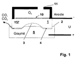
- FIG. 1 The simplest construction is in which a suitably shaped tool 1 made of YSZ is placed on the substrate surface 2 made of graphite.
- the ion-conductive ceramic is coated on the back with a thin electrically conductive layer 10, in this case of platinum, which nevertheless remains sufficiently permeable to oxygen.
- a voltage U is applied between the graphite and the back of the tool.
- it is necessary to heat the entire assembly to a temperature of about 400 ° C in an oxygen-containing atmosphere.
- the graphite is still stable to oxygen on the one hand, but on the other hand, the YSZ ceramic of the tool 1 has sufficient conductivity and the graphite is sufficiently reactive to an etching process in progress bring.
- the oxygen atmosphere O 2 ensures the actual supply of oxygen and prevents the formation of depletion zones in the ion conductor. Under these conditions, it is possible to achieve an etching rate around 12-30 nm / min at a voltage around 80V and a current density around 2 mA / cm 2 . However, a much higher etching rate is achievable. when a higher process temperature is applied. At temperatures above 500 ° C, however, it is absolutely necessary to protect or isolate the graphite from the oxygen.
- the YSZ tool 1 is connected at the back to a ceramic feed line 11, whose inner volume is supplied with an oxygen-containing atmosphere.
- the space outside of this tube is purged with a protective gas, nitrogen or argon. This largely avoids undesirable reaction of the graphite with oxygen radicals.
- a vertical vibrational motion such as ultra or megasonic can be initiated supportive.
- This method applies to the manufacture or replication of glassy carbon press tools. These tools are suitable as mold inserts in the blank pressing process of lenses for very high-melting materials such as silica glass.
Landscapes
- Engineering & Computer Science (AREA)
- Chemical & Material Sciences (AREA)
- Chemical Kinetics & Catalysis (AREA)
- Electrochemistry (AREA)
- Metallurgy (AREA)
- Manufacturing & Machinery (AREA)
- Microelectronics & Electronic Packaging (AREA)
- Materials Engineering (AREA)
- Mechanical Engineering (AREA)
- Organic Chemistry (AREA)
- Weting (AREA)
- Electroplating Methods And Accessories (AREA)
- ing And Chemical Polishing (AREA)
- Diffracting Gratings Or Hologram Optical Elements (AREA)
- Carbon And Carbon Compounds (AREA)
- Electrodes Of Semiconductors (AREA)
- Physical Vapour Deposition (AREA)
- Re-Forming, After-Treatment, Cutting And Transporting Of Glass Products (AREA)
Claims (7)
- Procédé pour le traitement de surface lors de la fabrication d'un outil de pressage en carbone vitreux pour le pressage à blanc de lentilles, dans lequel un outil présentant un matériau solide conduisant des ions sous la forme de ZrO2 est mis en contact, au moins par endroits, avec une surface de substrat en carbone vitreux, lequel est réalisé en tant que conducteur d'ions anionique, présente une surface d'outil structurée qui est apposée sur la surface du substrat, et auquel un potentiel électrique est appliqué, de sorte que des anions sortent du conducteur anionique dans des zones dans lesquelles l'outil est en contact avec la surface du substrat et se transforment à la surface du substrat en une combinaison réactive avec la surface du substrat, moyennant quoi la combinaison à capacité de réaction forme, avec le carbone vitreux, une combinaison gazeuse à la surface du substrat, de sorte qu'un processus d'enlèvement de matériau limité localement est réalisé, grâce auquel la surface du substrat est structurée quasiment à la manière d'un processus de décapage.
- Procédé selon la revendication 1,
caractérisé en ce que l'outil est pressé par application d'une force sur la surface du substrat. - Procédé selon les revendications 1 ou 2,
caractérisé en ce que l'outil présente un côté orienté vers la surface du substrat et un côté tournant le dos à celle-ci, et
en ce que le potentiel électrique est appliqué entre la surface du substrat et le côté de l'outil tournant le dos à la surface du substrat. - Procédé selon l'une des revendications 1 à 3,
caractérisé en ce que le matériau conduisant les anions de l'outil est sélectionné de manière à ce que les anions absorbés par la surface du substrat soient exclusivement transportés par l'outil sans modifier la composition chimique de celui-ci. - Procédé selon l'une des revendications 1 à 4,
caractérisé en ce que, en guise de réservoir, on prévoit un réservoir de forme gazeuse délivrant les anions sur le côté de l'outil tournant le dos à la surface du substrat. - Procédé selon la revendication 5,
caractérisé en ce que le réservoir est séparé spacialement du substrat de manière étanche aux gaz sur le côté de l'outil tournant le dos à la surface du substrat. - Procédé selon l'une des revendications 1 à 6,
caractérisé en ce que l'outil et/ou la surface du substrat sont exposés à des vibrations, de sorte que la combinaison gazeuse se formant entre la surface de l'outil et la surface du substrat s'échappe.
Applications Claiming Priority (3)
| Application Number | Priority Date | Filing Date | Title |
|---|---|---|---|
| DE102006019189 | 2006-04-21 | ||
| DE102006030323A DE102006030323A1 (de) | 2006-04-21 | 2006-06-30 | Verfahren zur Oberflächenbehandlung einer metallischen Substratoberfläche |
| EP07724433A EP2010351B1 (fr) | 2006-04-21 | 2007-04-20 | Procédé de traitement de surface d'un substrat métallique conducteur d'électricité. |
Related Parent Applications (2)
| Application Number | Title | Priority Date | Filing Date |
|---|---|---|---|
| EP07724433A Division EP2010351B1 (fr) | 2006-04-21 | 2007-04-20 | Procédé de traitement de surface d'un substrat métallique conducteur d'électricité. |
| EP07724433.3 Division | 2007-04-20 |
Publications (3)
| Publication Number | Publication Date |
|---|---|
| EP2058076A2 EP2058076A2 (fr) | 2009-05-13 |
| EP2058076A3 EP2058076A3 (fr) | 2013-02-13 |
| EP2058076B1 true EP2058076B1 (fr) | 2014-05-07 |
Family
ID=38536902
Family Applications (3)
| Application Number | Title | Priority Date | Filing Date |
|---|---|---|---|
| EP07724433A Active EP2010351B1 (fr) | 2006-04-21 | 2007-04-20 | Procédé de traitement de surface d'un substrat métallique conducteur d'électricité. |
| EP08022415.7A Active EP2058075B1 (fr) | 2006-04-21 | 2007-04-20 | Procédé de traitement de surfaces d'une surface de substrat conductrice électrique |
| EP08022416.5A Active EP2058076B1 (fr) | 2006-04-21 | 2007-04-20 | Procédé de traitement de surface d'un outil en carbone pour la production de lentilles. |
Family Applications Before (2)
| Application Number | Title | Priority Date | Filing Date |
|---|---|---|---|
| EP07724433A Active EP2010351B1 (fr) | 2006-04-21 | 2007-04-20 | Procédé de traitement de surface d'un substrat métallique conducteur d'électricité. |
| EP08022415.7A Active EP2058075B1 (fr) | 2006-04-21 | 2007-04-20 | Procédé de traitement de surfaces d'une surface de substrat conductrice électrique |
Country Status (5)
| Country | Link |
|---|---|
| US (1) | US8758590B2 (fr) |
| EP (3) | EP2010351B1 (fr) |
| JP (3) | JP5140661B2 (fr) |
| DE (1) | DE102006030323A1 (fr) |
| WO (1) | WO2007121948A2 (fr) |
Families Citing this family (4)
| Publication number | Priority date | Publication date | Assignee | Title |
|---|---|---|---|---|
| DE102009000073A1 (de) | 2009-01-08 | 2010-07-15 | Robert Bosch Gmbh | Verfahren und Vorrichtung zur elektrochemischen Bearbeitung von Substraten |
| CN104023889B (zh) * | 2011-12-06 | 2017-04-12 | 国立大学法人大阪大学 | 固体氧化物的加工方法及其装置 |
| WO2018052895A2 (fr) | 2016-09-16 | 2018-03-22 | 3M Innovative Properties Company | Procédé de fabrication d'un rouleau cylindrique nanostructuré |
| US12071733B2 (en) | 2022-08-18 | 2024-08-27 | Wirtgen Gmbh | Milling attachment with adjustable cover |
Family Cites Families (18)
| Publication number | Priority date | Publication date | Assignee | Title |
|---|---|---|---|---|
| NL204868A (fr) * | 1955-02-25 | |||
| US3653968A (en) | 1970-05-04 | 1972-04-04 | Union Carbide Corp | Solid state electrochemical cells |
| US4155735A (en) * | 1977-11-30 | 1979-05-22 | Ppg Industries, Inc. | Electromigration method for making stained glass photomasks |
| JPS5825488A (ja) | 1981-08-10 | 1983-02-15 | Tatsuya Suzuki | 金の回収装置 |
| JP2515510B2 (ja) * | 1986-08-26 | 1996-07-10 | 株式会社 ケミカル山本 | 鉄鋼材表面に施した亜鉛系被膜の除去方法 |
| US5034023A (en) | 1989-12-21 | 1991-07-23 | Corning Incorporated | Ceramic honeycomb structures as oxygen separators or concentrators |
| DE4242728A1 (de) * | 1992-12-17 | 1994-06-23 | Dornier Gmbh | Keramische Gasanschlußbauteile für Brennstoffzellen mit Zirkonoxid-Festelektrolyt |
| US5403619A (en) * | 1993-01-19 | 1995-04-04 | International Business Machines Corporation | Solid state ionic polishing of diamond |
| JP2000232078A (ja) * | 1999-02-10 | 2000-08-22 | Toshiba Corp | メッキ方法及びメッキ装置 |
| DE19960790B4 (de) * | 1999-12-16 | 2006-02-09 | Mtu Aero Engines Gmbh | Elektrode zum elektrochemischen Feinbohren von Werkstücken sowie Verfahren zu ihrer Herstellung |
| AU2002303842A1 (en) | 2001-05-22 | 2002-12-03 | Reflectivity, Inc. | A method for making a micromechanical device by removing a sacrificial layer with multiple sequential etchants |
| CN100407440C (zh) * | 2003-07-18 | 2008-07-30 | 日本电气株式会社 | 开关元件、驱动开关元件的方法、可重写的逻辑集成电路以及存储元件 |
| WO2005042810A2 (fr) * | 2003-10-31 | 2005-05-12 | E.I Du Pont De Nemours And Company | Electropolissage induit par une membrane |
| JP2005238420A (ja) * | 2004-02-27 | 2005-09-08 | Rikogaku Shinkokai | 固体中のイオンおよび/または原子の操作方法 |
| DE102004040217A1 (de) * | 2004-08-19 | 2006-03-02 | Mtu Aero Engines Gmbh | Elektrode zum elektrochemischen Senken |
| KR20080005991A (ko) * | 2005-04-29 | 2008-01-15 | 이 아이 듀폰 디 네모아 앤드 캄파니 | 지형적으로 패턴화된 막을 사용하는 막 매개 전해연마 |
| WO2007069725A1 (fr) * | 2005-12-15 | 2007-06-21 | Nec Corporation | Element de commutation et son procede de fabrication |
| US20070215480A1 (en) * | 2006-03-16 | 2007-09-20 | Fang Nicholas X | Pattern transfer by solid state electrochemical stamping |
-
2006
- 2006-06-30 DE DE102006030323A patent/DE102006030323A1/de not_active Ceased
-
2007
- 2007-04-20 JP JP2009505790A patent/JP5140661B2/ja active Active
- 2007-04-20 WO PCT/EP2007/003497 patent/WO2007121948A2/fr active Application Filing
- 2007-04-20 EP EP07724433A patent/EP2010351B1/fr active Active
- 2007-04-20 EP EP08022415.7A patent/EP2058075B1/fr active Active
- 2007-04-20 EP EP08022416.5A patent/EP2058076B1/fr active Active
- 2007-04-20 US US12/295,321 patent/US8758590B2/en active Active
-
2012
- 2012-09-12 JP JP2012200153A patent/JP5484538B2/ja active Active
- 2012-09-12 JP JP2012200152A patent/JP5640055B2/ja active Active
Also Published As
| Publication number | Publication date |
|---|---|
| DE102006030323A1 (de) | 2007-10-25 |
| US20090283416A1 (en) | 2009-11-19 |
| JP5640055B2 (ja) | 2014-12-10 |
| EP2058075A2 (fr) | 2009-05-13 |
| US8758590B2 (en) | 2014-06-24 |
| EP2058075A3 (fr) | 2013-02-13 |
| JP2009534523A (ja) | 2009-09-24 |
| EP2058075B1 (fr) | 2014-06-18 |
| WO2007121948A2 (fr) | 2007-11-01 |
| JP5484538B2 (ja) | 2014-05-07 |
| JP5140661B2 (ja) | 2013-02-06 |
| EP2058076A3 (fr) | 2013-02-13 |
| EP2010351B1 (fr) | 2012-06-27 |
| EP2058076A2 (fr) | 2009-05-13 |
| WO2007121948A3 (fr) | 2008-06-26 |
| EP2010351A2 (fr) | 2009-01-07 |
| JP2013032593A (ja) | 2013-02-14 |
| JP2013040406A (ja) | 2013-02-28 |
Similar Documents
| Publication | Publication Date | Title |
|---|---|---|
| DE69207888T2 (de) | Elektrochemisches Werkzeug zum gleichmässigen Metallabtrag beim Elektropolieren | |
| DE102018108798B4 (de) | Elektrodenstruktur und Verfahren zum Verbessern von RRAM-Leistung | |
| DE69426679T2 (de) | Vorrichtung und Verfahren zur Sicherstellung der Hitzeübertragung auf BZW von einem ganzen Substrat während der Bearbeitung eines Halbleiterbauteils | |
| US6972146B2 (en) | Structure having holes and method for producing the same | |
| US6914008B2 (en) | Structure having pores and its manufacturing method | |
| EP3592696B1 (fr) | Procédé et dispositif de mise à disposition d'une pluralité de nanofils | |
| EP2058076B1 (fr) | Procédé de traitement de surface d'un outil en carbone pour la production de lentilles. | |
| EP1829986B1 (fr) | Procédé de fonctionnement de surfaces d'un revêtement en carbone dur | |
| DE112011101910T5 (de) | Reduzieren von Kupfer- oder Spurenmetallverunreinigungen bei elektrolytischen Plasmaoxidationsbeschichtungen | |
| EP3028295B1 (fr) | Procédé de connexion de substrats | |
| US5468326A (en) | Apparatus for polishing a diamond or carbon nitride film by reaction with oxygen transported to the film through a superionic conductor in contact with the film | |
| EP3102717B1 (fr) | Couche protectrice pour nacelles pecvd en graphite | |
| DE102014019369B4 (de) | Halbleiterbauelement und herstellungsverfahren | |
| DE102017104905A1 (de) | Anordnung und Verfahren zum Bereitstellen einer Vielzahl von Nanodrähten sowie Galvanikkapsel | |
| Arya et al. | Investigation on deposition of the machined by-products and its reduction during electrochemical discharge machining (ECDM) | |
| EP3592697B1 (fr) | Dispositif et procédé de mise à disposition d'une pluralité de nanofils | |
| DE102015106896B4 (de) | Verfahren zur Bearbeitung eines Wafers | |
| DE102015117176B4 (de) | Verfahren zum Bearbeiten eines Trägers | |
| EP2828025B1 (fr) | Électrodes pour usinage d'une pièce ainsi que procédé pour la fabrication et l'utilisation de tels électrodes | |
| DE102008018742A1 (de) | Werkzeugelektrode zur elektrochemischen Bearbeitung und ein Verfahren für die elektrochemische Bearbeitung | |
| DE4433538A1 (de) | Verfahren zur Vermeidung der Re-Deposition von Ätzprodukten auf Substratoberflächen während des Wolfram-Rückätzprozesses bei der Herstellung hochintegrierter Schaltungen | |
| US20240131590A1 (en) | Methods of forming articles including microchannels therein, and related articles | |
| EP3983575B1 (fr) | Dispositif d'électrolyse comprenant deux couches de diamant dopées au bore | |
| Sviridova et al. | Direct nanosecond laser metallization of AlN ceramics | |
| EP4083274A2 (fr) | Électrode et procédé de production de celle-ci |
Legal Events
| Date | Code | Title | Description |
|---|---|---|---|
| PUAI | Public reference made under article 153(3) epc to a published international application that has entered the european phase |
Free format text: ORIGINAL CODE: 0009012 |
|
| 17P | Request for examination filed |
Effective date: 20081223 |
|
| AC | Divisional application: reference to earlier application |
Ref document number: 2010351 Country of ref document: EP Kind code of ref document: P |
|
| AK | Designated contracting states |
Kind code of ref document: A2 Designated state(s): AT BE BG CH CY CZ DE DK EE ES FI FR GB GR HU IE IS IT LI LT LU LV MC MT NL PL PT RO SE SI SK TR |
|
| RIC1 | Information provided on ipc code assigned before grant |
Ipc: B23H 3/00 20060101AFI20121113BHEP Ipc: C25D 3/00 20060101ALI20121113BHEP |
|
| PUAL | Search report despatched |
Free format text: ORIGINAL CODE: 0009013 |
|
| AK | Designated contracting states |
Kind code of ref document: A3 Designated state(s): AT BE BG CH CY CZ DE DK EE ES FI FR GB GR HU IE IS IT LI LT LU LV MC MT NL PL PT RO SE SI SK TR |
|
| RIC1 | Information provided on ipc code assigned before grant |
Ipc: C25D 3/00 20060101ALI20130109BHEP Ipc: B23H 3/00 20060101AFI20130109BHEP |
|
| AKX | Designation fees paid |
Designated state(s): AT BE BG CH CY CZ DE DK EE ES FI FR GB GR HU IE IS IT LI LT LU LV MC MT NL PL PT RO SE SI SK TR |
|
| GRAP | Despatch of communication of intention to grant a patent |
Free format text: ORIGINAL CODE: EPIDOSNIGR1 |
|
| INTG | Intention to grant announced |
Effective date: 20131219 |
|
| GRAS | Grant fee paid |
Free format text: ORIGINAL CODE: EPIDOSNIGR3 |
|
| GRAA | (expected) grant |
Free format text: ORIGINAL CODE: 0009210 |
|
| AC | Divisional application: reference to earlier application |
Ref document number: 2010351 Country of ref document: EP Kind code of ref document: P |
|
| AK | Designated contracting states |
Kind code of ref document: B1 Designated state(s): AT BE BG CH CY CZ DE DK EE ES FI FR GB GR HU IE IS IT LI LT LU LV MC MT NL PL PT RO SE SI SK TR |
|
| REG | Reference to a national code |
Ref country code: GB Ref legal event code: FG4D Free format text: NOT ENGLISH |
|
| REG | Reference to a national code |
Ref country code: AT Ref legal event code: REF Ref document number: 666200 Country of ref document: AT Kind code of ref document: T Effective date: 20140515 |
|
| REG | Reference to a national code |
Ref country code: IE Ref legal event code: FG4D Free format text: LANGUAGE OF EP DOCUMENT: GERMAN |
|
| REG | Reference to a national code |
Ref country code: DE Ref legal event code: R096 Ref document number: 502007013095 Country of ref document: DE Effective date: 20140618 |
|
| REG | Reference to a national code |
Ref country code: NL Ref legal event code: VDEP Effective date: 20140507 |
|
| REG | Reference to a national code |
Ref country code: LT Ref legal event code: MG4D |
|
| PG25 | Lapsed in a contracting state [announced via postgrant information from national office to epo] |
Ref country code: GR Free format text: LAPSE BECAUSE OF FAILURE TO SUBMIT A TRANSLATION OF THE DESCRIPTION OR TO PAY THE FEE WITHIN THE PRESCRIBED TIME-LIMIT Effective date: 20140808 Ref country code: IS Free format text: LAPSE BECAUSE OF FAILURE TO SUBMIT A TRANSLATION OF THE DESCRIPTION OR TO PAY THE FEE WITHIN THE PRESCRIBED TIME-LIMIT Effective date: 20140907 Ref country code: CY Free format text: LAPSE BECAUSE OF FAILURE TO SUBMIT A TRANSLATION OF THE DESCRIPTION OR TO PAY THE FEE WITHIN THE PRESCRIBED TIME-LIMIT Effective date: 20140507 Ref country code: LT Free format text: LAPSE BECAUSE OF FAILURE TO SUBMIT A TRANSLATION OF THE DESCRIPTION OR TO PAY THE FEE WITHIN THE PRESCRIBED TIME-LIMIT Effective date: 20140507 Ref country code: FI Free format text: LAPSE BECAUSE OF FAILURE TO SUBMIT A TRANSLATION OF THE DESCRIPTION OR TO PAY THE FEE WITHIN THE PRESCRIBED TIME-LIMIT Effective date: 20140507 |
|
| PG25 | Lapsed in a contracting state [announced via postgrant information from national office to epo] |
Ref country code: ES Free format text: LAPSE BECAUSE OF FAILURE TO SUBMIT A TRANSLATION OF THE DESCRIPTION OR TO PAY THE FEE WITHIN THE PRESCRIBED TIME-LIMIT Effective date: 20140507 Ref country code: SE Free format text: LAPSE BECAUSE OF FAILURE TO SUBMIT A TRANSLATION OF THE DESCRIPTION OR TO PAY THE FEE WITHIN THE PRESCRIBED TIME-LIMIT Effective date: 20140507 Ref country code: PL Free format text: LAPSE BECAUSE OF FAILURE TO SUBMIT A TRANSLATION OF THE DESCRIPTION OR TO PAY THE FEE WITHIN THE PRESCRIBED TIME-LIMIT Effective date: 20140507 Ref country code: LV Free format text: LAPSE BECAUSE OF FAILURE TO SUBMIT A TRANSLATION OF THE DESCRIPTION OR TO PAY THE FEE WITHIN THE PRESCRIBED TIME-LIMIT Effective date: 20140507 |
|
| PG25 | Lapsed in a contracting state [announced via postgrant information from national office to epo] |
Ref country code: PT Free format text: LAPSE BECAUSE OF FAILURE TO SUBMIT A TRANSLATION OF THE DESCRIPTION OR TO PAY THE FEE WITHIN THE PRESCRIBED TIME-LIMIT Effective date: 20140908 |
|
| PG25 | Lapsed in a contracting state [announced via postgrant information from national office to epo] |
Ref country code: CZ Free format text: LAPSE BECAUSE OF FAILURE TO SUBMIT A TRANSLATION OF THE DESCRIPTION OR TO PAY THE FEE WITHIN THE PRESCRIBED TIME-LIMIT Effective date: 20140507 Ref country code: DK Free format text: LAPSE BECAUSE OF FAILURE TO SUBMIT A TRANSLATION OF THE DESCRIPTION OR TO PAY THE FEE WITHIN THE PRESCRIBED TIME-LIMIT Effective date: 20140507 Ref country code: RO Free format text: LAPSE BECAUSE OF FAILURE TO SUBMIT A TRANSLATION OF THE DESCRIPTION OR TO PAY THE FEE WITHIN THE PRESCRIBED TIME-LIMIT Effective date: 20140507 Ref country code: EE Free format text: LAPSE BECAUSE OF FAILURE TO SUBMIT A TRANSLATION OF THE DESCRIPTION OR TO PAY THE FEE WITHIN THE PRESCRIBED TIME-LIMIT Effective date: 20140507 Ref country code: SK Free format text: LAPSE BECAUSE OF FAILURE TO SUBMIT A TRANSLATION OF THE DESCRIPTION OR TO PAY THE FEE WITHIN THE PRESCRIBED TIME-LIMIT Effective date: 20140507 |
|
| REG | Reference to a national code |
Ref country code: DE Ref legal event code: R097 Ref document number: 502007013095 Country of ref document: DE |
|
| PG25 | Lapsed in a contracting state [announced via postgrant information from national office to epo] |
Ref country code: NL Free format text: LAPSE BECAUSE OF FAILURE TO SUBMIT A TRANSLATION OF THE DESCRIPTION OR TO PAY THE FEE WITHIN THE PRESCRIBED TIME-LIMIT Effective date: 20140507 |
|
| PLBE | No opposition filed within time limit |
Free format text: ORIGINAL CODE: 0009261 |
|
| STAA | Information on the status of an ep patent application or granted ep patent |
Free format text: STATUS: NO OPPOSITION FILED WITHIN TIME LIMIT |
|
| 26N | No opposition filed |
Effective date: 20150210 |
|
| PG25 | Lapsed in a contracting state [announced via postgrant information from national office to epo] |
Ref country code: IT Free format text: LAPSE BECAUSE OF FAILURE TO SUBMIT A TRANSLATION OF THE DESCRIPTION OR TO PAY THE FEE WITHIN THE PRESCRIBED TIME-LIMIT Effective date: 20140507 |
|
| REG | Reference to a national code |
Ref country code: DE Ref legal event code: R097 Ref document number: 502007013095 Country of ref document: DE Effective date: 20150210 |
|
| PG25 | Lapsed in a contracting state [announced via postgrant information from national office to epo] |
Ref country code: SI Free format text: LAPSE BECAUSE OF FAILURE TO SUBMIT A TRANSLATION OF THE DESCRIPTION OR TO PAY THE FEE WITHIN THE PRESCRIBED TIME-LIMIT Effective date: 20140507 |
|
| PG25 | Lapsed in a contracting state [announced via postgrant information from national office to epo] |
Ref country code: LU Free format text: LAPSE BECAUSE OF FAILURE TO SUBMIT A TRANSLATION OF THE DESCRIPTION OR TO PAY THE FEE WITHIN THE PRESCRIBED TIME-LIMIT Effective date: 20150420 Ref country code: MC Free format text: LAPSE BECAUSE OF FAILURE TO SUBMIT A TRANSLATION OF THE DESCRIPTION OR TO PAY THE FEE WITHIN THE PRESCRIBED TIME-LIMIT Effective date: 20140507 |
|
| REG | Reference to a national code |
Ref country code: CH Ref legal event code: PL |
|
| REG | Reference to a national code |
Ref country code: IE Ref legal event code: MM4A |
|
| PG25 | Lapsed in a contracting state [announced via postgrant information from national office to epo] |
Ref country code: CH Free format text: LAPSE BECAUSE OF NON-PAYMENT OF DUE FEES Effective date: 20150430 Ref country code: LI Free format text: LAPSE BECAUSE OF NON-PAYMENT OF DUE FEES Effective date: 20150430 |
|
| REG | Reference to a national code |
Ref country code: FR Ref legal event code: PLFP Year of fee payment: 10 |
|
| PG25 | Lapsed in a contracting state [announced via postgrant information from national office to epo] |
Ref country code: IE Free format text: LAPSE BECAUSE OF NON-PAYMENT OF DUE FEES Effective date: 20150420 |
|
| REG | Reference to a national code |
Ref country code: AT Ref legal event code: MM01 Ref document number: 666200 Country of ref document: AT Kind code of ref document: T Effective date: 20150420 |
|
| PG25 | Lapsed in a contracting state [announced via postgrant information from national office to epo] |
Ref country code: AT Free format text: LAPSE BECAUSE OF NON-PAYMENT OF DUE FEES Effective date: 20150420 |
|
| PG25 | Lapsed in a contracting state [announced via postgrant information from national office to epo] |
Ref country code: MT Free format text: LAPSE BECAUSE OF FAILURE TO SUBMIT A TRANSLATION OF THE DESCRIPTION OR TO PAY THE FEE WITHIN THE PRESCRIBED TIME-LIMIT Effective date: 20140507 |
|
| REG | Reference to a national code |
Ref country code: FR Ref legal event code: PLFP Year of fee payment: 11 |
|
| PG25 | Lapsed in a contracting state [announced via postgrant information from national office to epo] |
Ref country code: HU Free format text: LAPSE BECAUSE OF FAILURE TO SUBMIT A TRANSLATION OF THE DESCRIPTION OR TO PAY THE FEE WITHIN THE PRESCRIBED TIME-LIMIT; INVALID AB INITIO Effective date: 20070420 Ref country code: BG Free format text: LAPSE BECAUSE OF FAILURE TO SUBMIT A TRANSLATION OF THE DESCRIPTION OR TO PAY THE FEE WITHIN THE PRESCRIBED TIME-LIMIT Effective date: 20140507 |
|
| PG25 | Lapsed in a contracting state [announced via postgrant information from national office to epo] |
Ref country code: BE Free format text: LAPSE BECAUSE OF NON-PAYMENT OF DUE FEES Effective date: 20150430 |
|
| PG25 | Lapsed in a contracting state [announced via postgrant information from national office to epo] |
Ref country code: TR Free format text: LAPSE BECAUSE OF FAILURE TO SUBMIT A TRANSLATION OF THE DESCRIPTION OR TO PAY THE FEE WITHIN THE PRESCRIBED TIME-LIMIT Effective date: 20140507 |
|
| REG | Reference to a national code |
Ref country code: FR Ref legal event code: PLFP Year of fee payment: 12 |
|
| P01 | Opt-out of the competence of the unified patent court (upc) registered |
Effective date: 20230524 |
|
| PGFP | Annual fee paid to national office [announced via postgrant information from national office to epo] |
Ref country code: GB Payment date: 20240423 Year of fee payment: 18 |
|
| PGFP | Annual fee paid to national office [announced via postgrant information from national office to epo] |
Ref country code: DE Payment date: 20240418 Year of fee payment: 18 |
|
| PGFP | Annual fee paid to national office [announced via postgrant information from national office to epo] |
Ref country code: FR Payment date: 20240423 Year of fee payment: 18 |