EP2058070A1 - Cutting tool, process for producing the same, and method of cutting - Google Patents
Cutting tool, process for producing the same, and method of cutting Download PDFInfo
- Publication number
- EP2058070A1 EP2058070A1 EP07806399A EP07806399A EP2058070A1 EP 2058070 A1 EP2058070 A1 EP 2058070A1 EP 07806399 A EP07806399 A EP 07806399A EP 07806399 A EP07806399 A EP 07806399A EP 2058070 A1 EP2058070 A1 EP 2058070A1
- Authority
- EP
- European Patent Office
- Prior art keywords
- substrate
- phase
- tin layer
- cutting tool
- cutting
- Prior art date
- Legal status (The legal status is an assumption and is not a legal conclusion. Google has not performed a legal analysis and makes no representation as to the accuracy of the status listed.)
- Granted
Links
Images

Classifications
-
- B—PERFORMING OPERATIONS; TRANSPORTING
- B23—MACHINE TOOLS; METAL-WORKING NOT OTHERWISE PROVIDED FOR
- B23B—TURNING; BORING
- B23B27/00—Tools for turning or boring machines; Tools of a similar kind in general; Accessories therefor
- B23B27/14—Cutting tools of which the bits or tips or cutting inserts are of special material
- B23B27/141—Specially shaped plate-like cutting inserts, i.e. length greater or equal to width, width greater than or equal to thickness
- B23B27/145—Specially shaped plate-like cutting inserts, i.e. length greater or equal to width, width greater than or equal to thickness characterised by having a special shape
- B23B27/146—Means to improve the adhesion between the substrate and the coating
-
- B—PERFORMING OPERATIONS; TRANSPORTING
- B22—CASTING; POWDER METALLURGY
- B22F—WORKING METALLIC POWDER; MANUFACTURE OF ARTICLES FROM METALLIC POWDER; MAKING METALLIC POWDER; APPARATUS OR DEVICES SPECIALLY ADAPTED FOR METALLIC POWDER
- B22F7/00—Manufacture of composite layers, workpieces, or articles, comprising metallic powder, by sintering the powder, with or without compacting wherein at least one part is obtained by sintering or compression
- B22F7/06—Manufacture of composite layers, workpieces, or articles, comprising metallic powder, by sintering the powder, with or without compacting wherein at least one part is obtained by sintering or compression of composite workpieces or articles from parts, e.g. to form tipped tools
- B22F7/08—Manufacture of composite layers, workpieces, or articles, comprising metallic powder, by sintering the powder, with or without compacting wherein at least one part is obtained by sintering or compression of composite workpieces or articles from parts, e.g. to form tipped tools with one or more parts not made from powder
-
- C—CHEMISTRY; METALLURGY
- C22—METALLURGY; FERROUS OR NON-FERROUS ALLOYS; TREATMENT OF ALLOYS OR NON-FERROUS METALS
- C22C—ALLOYS
- C22C29/00—Alloys based on carbides, oxides, nitrides, borides, or silicides, e.g. cermets, or other metal compounds, e.g. oxynitrides, sulfides
- C22C29/02—Alloys based on carbides, oxides, nitrides, borides, or silicides, e.g. cermets, or other metal compounds, e.g. oxynitrides, sulfides based on carbides or carbonitrides
-
- C—CHEMISTRY; METALLURGY
- C23—COATING METALLIC MATERIAL; COATING MATERIAL WITH METALLIC MATERIAL; CHEMICAL SURFACE TREATMENT; DIFFUSION TREATMENT OF METALLIC MATERIAL; COATING BY VACUUM EVAPORATION, BY SPUTTERING, BY ION IMPLANTATION OR BY CHEMICAL VAPOUR DEPOSITION, IN GENERAL; INHIBITING CORROSION OF METALLIC MATERIAL OR INCRUSTATION IN GENERAL
- C23C—COATING METALLIC MATERIAL; COATING MATERIAL WITH METALLIC MATERIAL; SURFACE TREATMENT OF METALLIC MATERIAL BY DIFFUSION INTO THE SURFACE, BY CHEMICAL CONVERSION OR SUBSTITUTION; COATING BY VACUUM EVAPORATION, BY SPUTTERING, BY ION IMPLANTATION OR BY CHEMICAL VAPOUR DEPOSITION, IN GENERAL
- C23C16/00—Chemical coating by decomposition of gaseous compounds, without leaving reaction products of surface material in the coating, i.e. chemical vapour deposition [CVD] processes
- C23C16/22—Chemical coating by decomposition of gaseous compounds, without leaving reaction products of surface material in the coating, i.e. chemical vapour deposition [CVD] processes characterised by the deposition of inorganic material, other than metallic material
- C23C16/30—Deposition of compounds, mixtures or solid solutions, e.g. borides, carbides, nitrides
- C23C16/34—Nitrides
-
- C—CHEMISTRY; METALLURGY
- C23—COATING METALLIC MATERIAL; COATING MATERIAL WITH METALLIC MATERIAL; CHEMICAL SURFACE TREATMENT; DIFFUSION TREATMENT OF METALLIC MATERIAL; COATING BY VACUUM EVAPORATION, BY SPUTTERING, BY ION IMPLANTATION OR BY CHEMICAL VAPOUR DEPOSITION, IN GENERAL; INHIBITING CORROSION OF METALLIC MATERIAL OR INCRUSTATION IN GENERAL
- C23C—COATING METALLIC MATERIAL; COATING MATERIAL WITH METALLIC MATERIAL; SURFACE TREATMENT OF METALLIC MATERIAL BY DIFFUSION INTO THE SURFACE, BY CHEMICAL CONVERSION OR SUBSTITUTION; COATING BY VACUUM EVAPORATION, BY SPUTTERING, BY ION IMPLANTATION OR BY CHEMICAL VAPOUR DEPOSITION, IN GENERAL
- C23C16/00—Chemical coating by decomposition of gaseous compounds, without leaving reaction products of surface material in the coating, i.e. chemical vapour deposition [CVD] processes
- C23C16/44—Chemical coating by decomposition of gaseous compounds, without leaving reaction products of surface material in the coating, i.e. chemical vapour deposition [CVD] processes characterised by the method of coating
-
- C—CHEMISTRY; METALLURGY
- C23—COATING METALLIC MATERIAL; COATING MATERIAL WITH METALLIC MATERIAL; CHEMICAL SURFACE TREATMENT; DIFFUSION TREATMENT OF METALLIC MATERIAL; COATING BY VACUUM EVAPORATION, BY SPUTTERING, BY ION IMPLANTATION OR BY CHEMICAL VAPOUR DEPOSITION, IN GENERAL; INHIBITING CORROSION OF METALLIC MATERIAL OR INCRUSTATION IN GENERAL
- C23C—COATING METALLIC MATERIAL; COATING MATERIAL WITH METALLIC MATERIAL; SURFACE TREATMENT OF METALLIC MATERIAL BY DIFFUSION INTO THE SURFACE, BY CHEMICAL CONVERSION OR SUBSTITUTION; COATING BY VACUUM EVAPORATION, BY SPUTTERING, BY ION IMPLANTATION OR BY CHEMICAL VAPOUR DEPOSITION, IN GENERAL
- C23C30/00—Coating with metallic material characterised only by the composition of the metallic material, i.e. not characterised by the coating process
- C23C30/005—Coating with metallic material characterised only by the composition of the metallic material, i.e. not characterised by the coating process on hard metal substrates
-
- B—PERFORMING OPERATIONS; TRANSPORTING
- B22—CASTING; POWDER METALLURGY
- B22F—WORKING METALLIC POWDER; MANUFACTURE OF ARTICLES FROM METALLIC POWDER; MAKING METALLIC POWDER; APPARATUS OR DEVICES SPECIALLY ADAPTED FOR METALLIC POWDER
- B22F5/00—Manufacture of workpieces or articles from metallic powder characterised by the special shape of the product
- B22F2005/001—Cutting tools, earth boring or grinding tool other than table ware
-
- B—PERFORMING OPERATIONS; TRANSPORTING
- B22—CASTING; POWDER METALLURGY
- B22F—WORKING METALLIC POWDER; MANUFACTURE OF ARTICLES FROM METALLIC POWDER; MAKING METALLIC POWDER; APPARATUS OR DEVICES SPECIALLY ADAPTED FOR METALLIC POWDER
- B22F2999/00—Aspects linked to processes or compositions used in powder metallurgy
-
- B—PERFORMING OPERATIONS; TRANSPORTING
- B23—MACHINE TOOLS; METAL-WORKING NOT OTHERWISE PROVIDED FOR
- B23B—TURNING; BORING
- B23B2224/00—Materials of tools or workpieces composed of a compound including a metal
- B23B2224/36—Titanium nitride
-
- B—PERFORMING OPERATIONS; TRANSPORTING
- B23—MACHINE TOOLS; METAL-WORKING NOT OTHERWISE PROVIDED FOR
- B23B—TURNING; BORING
- B23B2228/00—Properties of materials of tools or workpieces, materials of tools or workpieces applied in a specific manner
- B23B2228/10—Coatings
-
- C—CHEMISTRY; METALLURGY
- C22—METALLURGY; FERROUS OR NON-FERROUS ALLOYS; TREATMENT OF ALLOYS OR NON-FERROUS METALS
- C22C—ALLOYS
- C22C2204/00—End product comprising different layers, coatings or parts of cermet
-
- Y—GENERAL TAGGING OF NEW TECHNOLOGICAL DEVELOPMENTS; GENERAL TAGGING OF CROSS-SECTIONAL TECHNOLOGIES SPANNING OVER SEVERAL SECTIONS OF THE IPC; TECHNICAL SUBJECTS COVERED BY FORMER USPC CROSS-REFERENCE ART COLLECTIONS [XRACs] AND DIGESTS
- Y10—TECHNICAL SUBJECTS COVERED BY FORMER USPC
- Y10T—TECHNICAL SUBJECTS COVERED BY FORMER US CLASSIFICATION
- Y10T428/00—Stock material or miscellaneous articles
- Y10T428/26—Web or sheet containing structurally defined element or component, the element or component having a specified physical dimension
-
- Y—GENERAL TAGGING OF NEW TECHNOLOGICAL DEVELOPMENTS; GENERAL TAGGING OF CROSS-SECTIONAL TECHNOLOGIES SPANNING OVER SEVERAL SECTIONS OF THE IPC; TECHNICAL SUBJECTS COVERED BY FORMER USPC CROSS-REFERENCE ART COLLECTIONS [XRACs] AND DIGESTS
- Y10—TECHNICAL SUBJECTS COVERED BY FORMER USPC
- Y10T—TECHNICAL SUBJECTS COVERED BY FORMER US CLASSIFICATION
- Y10T428/00—Stock material or miscellaneous articles
- Y10T428/26—Web or sheet containing structurally defined element or component, the element or component having a specified physical dimension
- Y10T428/268—Monolayer with structurally defined element
-
- Y—GENERAL TAGGING OF NEW TECHNOLOGICAL DEVELOPMENTS; GENERAL TAGGING OF CROSS-SECTIONAL TECHNOLOGIES SPANNING OVER SEVERAL SECTIONS OF THE IPC; TECHNICAL SUBJECTS COVERED BY FORMER USPC CROSS-REFERENCE ART COLLECTIONS [XRACs] AND DIGESTS
- Y10—TECHNICAL SUBJECTS COVERED BY FORMER USPC
- Y10T—TECHNICAL SUBJECTS COVERED BY FORMER US CLASSIFICATION
- Y10T428/00—Stock material or miscellaneous articles
- Y10T428/31504—Composite [nonstructural laminate]
- Y10T428/31678—Of metal
-
- Y—GENERAL TAGGING OF NEW TECHNOLOGICAL DEVELOPMENTS; GENERAL TAGGING OF CROSS-SECTIONAL TECHNOLOGIES SPANNING OVER SEVERAL SECTIONS OF THE IPC; TECHNICAL SUBJECTS COVERED BY FORMER USPC CROSS-REFERENCE ART COLLECTIONS [XRACs] AND DIGESTS
- Y10—TECHNICAL SUBJECTS COVERED BY FORMER USPC
- Y10T—TECHNICAL SUBJECTS COVERED BY FORMER US CLASSIFICATION
- Y10T83/00—Cutting
- Y10T83/04—Processes
Definitions
- the present invention relates to a cutting tool used in metal cutting or the like, a method of producing the same, and a cutting method using the same.
- Hard materials obtained by coating TiC, TiCN, TiN, or Al 2 O 3 , on a surface of a substrate made of, for example, cemented carbide or cermet using a chemical vapor deposition (CVD) or a physical vapor deposition (PVD) are conventionally used in a cutting tool.
- CVD chemical vapor deposition
- PVD physical vapor deposition
- Such a cutting tool is widely used in a variety of fields such as metal cutting work due to wear resistance of its coating layer(s) and toughness of its substrate.
- Patent Document 1 a method of improving adhesion between the substrate and the coating layer(s), in which the surface of the substrate is roughened to increase its surface area so as to obtain an anchor effect (refer to Patent Document 1), have been conventionally proposed. Also, there has been proposed a method of improving adhesion between the substrate and the coating layer(s) by diffusing constitutive elements of the substrate to the coating layer(s)(refer to Patent Documents 2 or 3).
- a first layer of TiC or TiN, a second layer of TiCN including columnar crystal, a third layer of TiC, TiCO or the like, and a fourth layer of Al 2 O 3 are sequentially coated on the surface made of WC-based cemented carbide containing Co using the CVD method, in which components W and Co contained in the substrate are diffused to the first and second layers or to the first to third layers.
- the diffusion layer is obviously non-uniform when closely observing the diffusion inside of the coating layer(s) from the surface of the substrate. Specifically, a diffusion amount is very high in a part where a Co component serving as a binding metal is exposed on the surface of the substrate. However, the diffusion is not sufficient in a part having the surface of a cubic structure compound such as tungsten carbide. Therefore, there has been a problem that the adhesion between the substrate and the coating layer(s) cannot be sufficiently improved.
- the invention aims to provide a cutting tool made of hard materials having improved adhesion between a substrate made of cemented carbide obtained by combining a hard phase with a binding metal and a TiN layer deposited on the surface of the substrate, and a method of processing the same.
- a cutting tool is made of a hard material, wherein: the hard material has a substrate including a hard material and a binding metal and a TiN layer deposited thereon; the substrate has a ⁇ -phase of solid solution of at least one type selected from a group consisting of carbide, nitride, and carbonitride containing W and a material selected from a group consisting of Ti, Ta, Nb, and Zr; at least part of the ⁇ -phase is formed on the surface of the substrate; and the TiN layer has crystals, which have the same orientation as the ⁇ -phase, right above the ⁇ -phase.
- a method of producing a cutting tool made of a hard material according to the present invention includes: a process for grinding a substrate including a hard material, a binding metal, and a ⁇ -phase made of solid solution of at least one type selected from a group consisting of carbide, nitride, and carbonitride containing W and a material selected from a group consisting of Ti, Ta, Nb, and Zr to expose the ⁇ -phase on a surface of the substrate; a pre-process process for oxidization reduction of the surface of the substrate and generation of N dangling bonds on the surface of the substrate; and a forming process of a TiN layer for forming a TiN layer having an epitaxial growth portion right above the ⁇ -phase exposed on the surface of the substrate using chemical vapor deposition.
- the present invention it is possible to improve adhesion between the substrate and the coating layer(s). This makes it possible to prevent defects caused by film peeling that can occur in the cutting process, and to provide a cutting tool having improved fracture resistance.
- the invention relates to a cutting tool used in cutting metals or the like.
- the invention relates to a cutting tool made of hard materials which include a substrate made of cemented carbide obtained by combining a hard phase with a binding metal, and at least a TiN layer deposited on the surface of the substrate.
- the cutting tool described above may include tools having a cutting egde part to contribute to the cutting, such as a solid type drill or an a solid type endmill, or a chip used in a soldering type or throw-away type turning tool.
- a substrate of the present invention includes a hard phase and binding metal.
- the hard phase of the present invention includes at least one type of material selected from a carbide, nitride, and carbonitride of metal in groups IV, V, and VI of the periodic table. Specifically, it contains tungsten carbide (WC) as a main component, and also contains titanium carbide, tantalum carbide, niobium carbide, zirconium carbide, or the like as subsidiary components.
- WC tungsten carbide
- Any binding metal conventionally used in the art can be used.
- iron group metals such as Fe, Ni, or Co can be used.
- a coating layer is deposited on the surface of the substrate.
- the coating layer may be a single layer or a multilayer.
- a TiN layer is deposited closest to the substrate in the coating layer(s).
- a TiCN layer e.g, including columnar crystal, a TiC layer, a TiCO layer, an Al 2 O 3 layer are appropriately deposited on the TiN layer.
- a substrate according to the present invention has a ⁇ -phase made of solid solution of at least one type selected from a group consisting of carbide, nitride, and carbonitride containing W and a material selected from a group consisting of Ti, Ta, Nb, and Zr.
- the TiN layer has a crystal, right above the ⁇ -phase at the surface of the substrate, having the same orientation as that of the ⁇ -phase (i.e., an epitaxial). That is, the TiN layer has portions epitaxially grown on the ⁇ -phase in an interface with the substrate. This improves adhesion between the substrate and the coating layer (s).
- Epitaxial growth means a process of growing crystals on a substrate, the crystals having the same orientation as the substrate.
- Epitaxially grown crystals can be examined by analyzing that the stripes (lattice fringes) of the crystal lattices are apparently continuous from the ⁇ -phase of the substrate to grains of the TiN layer right above thereof when observing the ⁇ -phase and grains of the TiN layer with a magnification of x2, 000,000 using a transmission electron microscope and analyzing that the ⁇ -phase and the TiN grain can be seen as images indicating the same lattice structure in selected-area electron diffraction images thereof.
- the substrate contains the ⁇ -phase crystals within the range of 1 to 8 wt%. Within this range, the adhesion between the TiN layer and the substrate and the strength of the substrate are well balanced. For this reason, wear resistance and defect resistance of the cutting tool are improved.
- the substrate contains 1 wt% or more of ⁇ -phase crystals, the area occupied by the TiN layer epitaxially grown on the ⁇ -phase increases. Also, the adhesion between the substrate and the TiN layer is likely to be improved.
- the substrate contains 8 wt% or less ⁇ -phase crystals, they are appropriately distributed and seldom agglomerated in the substrate. This restrains generation of agglomerated portions of the ⁇ -phase that may act as an origin for destruction, and allows the tool to attain further improved fracture resistance.
- the interface between the substrate and the TiN layer has Rmax of 0. 05 to 0. 35 ⁇ m with respect to a reference length of 10 ⁇ m. Particularly, it is more preferable to have Rmax of 0.1 to 0.2 ⁇ m.
- the processed surface is appropriately active, and the surface of the substrate can be prevented from being excessively oxidized after processing, therefore the TiN layer can epitaxially grow on the ⁇ -phases readily.
- Rmax is 0.35 ⁇ m or lower, the surface is kept smooth, and thus, the TiN layer can epitaxially grow on the ⁇ -phase readily.
- the average width of TiN crystals in a perpendicular direction with respect to the direction of the thickness of the TiN layer is within 10 to 50 nm, adhesion can be much improved to allow for easier epitaxial growth.
- the average width of TiN crystals is preferably set to 10 to 30 nm.
- the average width of TiN crystals in a perpendicular direction with respect to the direction of the thickness of the TiN layer is 10 nm or more, grain boundaries in a unit area are not excessively increased and thus an area for epitaxial growth is ensured.
- the average width of TiN crystals in a perpendicular direction with respect to the direction of the thickness of the TiN layer is 50 nm or less, the strength of the TiN grain is still maintained and thus the TiN layer is hard to destroy or render to fracture, even when a hard impact is applied.
- tungsten carbide (WC) powder is mixed with metal cobalt powder (Co) of 5.0 to 15.0 vol% and, as compound powder for forming the ⁇ -phase, titanium carbide powder of 0.8 to 4.5 vol%, and tantalum carbide of 0.5 to 7.0 vol%.
- Co metal cobalt powder
- the powder mixed as described above is blended and pulverized into slurry, a binder is added to the slurry, and then, the slurry is dried using a spray drier or the like, so as to granulate the blended powder. Subsequently, press-molding is performed using the granulized powder to mold a cutting tool. Then, the molded powder compact is degreased in a sintering furnace, and then sintered at a temperature of 1420 to 1550 degrees in Celsius for 1 to 1.5 hours, thereby producing cemented carbide.
- the surface of the substrate made of the cemented carbide is ground with a brush using an abrasive grain having the size of about #400 to 1000.
- This allows the ⁇ -phase of solid solution of at least one type selected from a group consisting of carbide, nitride, and carbonitride containing W and a material selected from a group consisting of Ti, Ta, Nb, and Zr to be exposed.
- this makes it possible to prepare the substrate in a state such that the TiN layer can epitaxially grow on the ⁇ -phase readily.
- the rotation number, the pressure and the like of the brush in the grinding process are adequately adjusted so as to provide an interface between the substrate and the TiN layer having Rmax of 0.05 to 0.35 ⁇ m with respect to the reference length of 10 ⁇ m.
- the grinding process using the brush is preferable in comparison with other methods such as sand blasting or etching, by which surface roughness is likely to increase, since the surface roughness can be adjusted to within the aforementioned range by the grinding process using the brush.
- a mixed gas containing H 2 of 50 to 75 vol% and N 2 of 25 to 50 vol% totalized to 100 vol% is introduced to a CVD furnace.
- the CVD furnace is controlled so that the value Vg/Vr (l/min) is in the range from 0.1 to 0.3 when the volume of the introduced gas at ordinary temperature and pressure is Vg (L/min), and the volume of the CVD furnace is Vr(L).
- the substrate is held in the CVD furnace.
- the object of this pre-process is reduction of oxidization of the surface of the substrate and generation of N dangling bonds on the surface of the substrate.
- the TiN layer deposited on the surface of the substrate to have the crystal of the same orientation as that of the ⁇ -phase of the surface of the substrate. That is, it is possible to make the TiN layer to epitaxially grow with the ⁇ -phase on the surface of the substrate readily.
- the pre-process is performed in a time period of 10 to 60 minutes, with the pressure in the CVD furnace of 10 to 30 kPa, and a processing temperature of 850 to 950 degrees in Celsius.
- the surface of the substrate will be in a condition that allows epitaxial growth to occur readily.
- a mixed gas containing TiCl 4 of 0.3 to 1.2 vol%, H 2 of 35 to 65 vol%, and N 2 of 35 to 65 vol% totalized to 100 vol% is introduced to a CVD furnace.
- the CVD furnace is controlled so that the value Vg/Vr (l/min) is in the range from 0.7 to 1.1 under a constant pressure.
- the TiN layer having an epitaxially grown part on the ⁇ -phase exposed at the surface of the substrate is deposited using a CVD method.
- Vg (L/min)
- the value of Vg (L/min) is large. That is, the amount of the introduced gas significantly increases in comparison with the pre-process. In this condition, the velocity of the gas flowing through the CVD furnace increases in a constant pressure atmosphere. This makes it possible to supply the energy required for epitaxial growth of the TiN layer deposited by the CVD method as kinetic energy.
- the pressure is set to 7 to 20kPa, and the processing temperature is set to 860 to 1000 degrees in Celsius. These ranges readily allow the TiN layer to grow epitaxially on the surface of the substrate.
- the TiN layer As described in the aforementioned producing method, it is possible for the TiN layer to grow epitaxially on the ⁇ -phase exposed at the surface of the substrate by performing a prescribed depositing process of the TiN layer after a prescribed grinding process and a prescribed pre-process. Also, it is possible to improve adhesion between the coating layer (s) including the TiN layer and the substrate.
- the grinding process according to the present invention provides a mirror finished surface or Rmax of 0.05 ⁇ m or less.
- cemented carbide which is the material of the substrate, has a hexagonal crystal such as tungsten carbide
- the TiN layer has a cubical crystal. Since they have different crystal structures, it has been very difficult to match the crystal orientation of the TiN layer deposited on the surface of the substrate with that of the ⁇ -phase, and it has been necessary to form mismatch dislocations or the like.
- the applicant succeeded in epitaxial growth of the TiN layer on the ⁇ -phase in the interface with the substrate, which has not been possible conventionally, by sequentially performing: (1) a grinding process for exposing the ⁇ -phase made of at least one type of solid solution selected from a group consisting of carbide, nitride, and carbonitride containing W and a material selected from a group consisting of Ti, Ta, Nb, and Zr at the surface of the substrate and smoothing the surface of the substrate; (2) a pre-process for oxidization reduction of the surface of the substrate and generation of N dangling bonds on the surface of the substrate; and (3) a forming process of the TiN layer by generating gas flow in the CVD furnace in a prescribed condition to supply energy required for the epitaxial growth of the TiN layer.
- the mixed powder is molded in the shape of a cutting tool (CNMG120408) using a press-molding. After a binder removal process, the molded cutting tool is sintered under the conditions shown in Table 1, thereby producing cemented carbide (sample Nos. A to D). [Table 1] Sample No.
- the amount of ⁇ -phase crystals included in the cemented carbide was measured for sample Nos. A to D using X-ray fluorescence (XRF), and carbide conversion and volume conversion were calculated to obtain No. A sample of 1.4 vol%, No. B sample of 8 vol%, No. C sample of 1 vol%, and No. D sample of 0 vol%.
- XRF X-ray fluorescence
- Samples No. 1 to 15 were prepared using the cemented carbide samples Nos. A to D as substrates, and the respective grinding processes were applied to the surfaces of samples as shown in Table 2.
- the layer thicknesses in Table 2 were obtained by: taking scanning electron microscope (SEM) photos for 5 points in arbitrary cross-sections, each of which includes an interface between the substrate and the coating layer(s) or an interface between coating layers; measuring respective layer thicknesses for some points; and averaging the measured values.
- SEM scanning electron microscope
- the TiN layer includes the crystals, which have the same orientation as the ⁇ -phase, right above the ⁇ -phase on the surface of the substrate, i.e., whether or not epitaxial growth is achieved, was examined by using selected-area electron diffraction.
- the inventors observed cross-sections of an interface between each base material and the TiN layer by using high resolution transmission electron microscope analysis (HR-TEM) to determine that the TiN layer has the same orientation as the ⁇ -phase if TiN has an area having lattice fringes apparently continuous from the ⁇ -phase of the base material in a multiple wave interference image.
- HR-TEM high resolution transmission electron microscope analysis
- Fig. 1 is a schematic diagram illustrating a cross-section for examining epitaxial growth in an interface between the substrate and the coating layer(s).
- a cutting test was performed under the conditions described below using No. 1 to 15 samples. Wear resistance (flank wear, boundary wear), defect resistance, and cutting edge states were measured for each sample. The results are shown in Table 4.
- the TiN layer includes crystals, which have the same orientation with the ⁇ -phase, on the ⁇ -phase, adhesion between the substrate and the coating layer(s) is improved in the portion and thus any fracture that could have been generated during cutting was prevented. Also it can be considered that pressure in a part where the pressure is usually concentrated could be suppressed, and thus durability of the cutting tool could be improved.
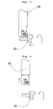
- Figs. 2 to 4 are schematic diagrams illustrating a cutting method according to the present invention.
- a cutting tool 15 and a work 20 to be cut are prepared. While the work 20 is rotated, the cutting tool 15 approaches the work 20. Alternatively, the work 20 may approach the cutting tool 15 to bring the tool 15 and the work 20 closer to each other.
- the work is cut by allowing the cutting tool 15 to make contact with the work material 20.
- the cutting tool 15 is separated from the work 20.
- the cutting tool 15 can repeatedly make contact with different spots on the work 20 while the work is continuously rotated.
Landscapes
- Chemical & Material Sciences (AREA)
- Mechanical Engineering (AREA)
- Engineering & Computer Science (AREA)
- Materials Engineering (AREA)
- Organic Chemistry (AREA)
- Metallurgy (AREA)
- Chemical Kinetics & Catalysis (AREA)
- General Chemical & Material Sciences (AREA)
- Composite Materials (AREA)
- Manufacturing & Machinery (AREA)
- Inorganic Chemistry (AREA)
- Cutting Tools, Boring Holders, And Turrets (AREA)
- Chemical Vapour Deposition (AREA)
- Powder Metallurgy (AREA)
Abstract
Description
- The present invention relates to a cutting tool used in metal cutting or the like, a method of producing the same, and a cutting method using the same.
- Hard materials obtained by coating TiC, TiCN, TiN, or Al2O3, on a surface of a substrate made of, for example, cemented carbide or cermet using a chemical vapor deposition (CVD) or a physical vapor deposition (PVD) are conventionally used in a cutting tool. Such a cutting tool is widely used in a variety of fields such as metal cutting work due to wear resistance of its coating layer(s) and toughness of its substrate.
- However, there has been a problem that if such a cutting tool has weak adhesion between the substrate and the coating layer (s) deposited thereon, the coating layer (s) may be peeled from the substrate during the cutting process, and the cutting tool may rapidly wear down, reducing its lifetime. There has been another problem that if hard impact is applied to the cutting edge during the cutting process, the coating layer(s) may be peeled due to the weak adhesion between the substrate and the coating layer(s) deposited thereon, and the cutting tool may be fractured.
- In order to solve the aforementioned problems, a method of improving adhesion between the substrate and the coating layer(s), in which the surface of the substrate is roughened to increase its surface area so as to obtain an anchor effect (refer to Patent Document 1), have been conventionally proposed. Also, there has been proposed a method of improving adhesion between the substrate and the coating layer(s) by diffusing constitutive elements of the substrate to the coating layer(s)(refer to
Patent Documents 2 or 3). - Specifically, a first layer of TiC or TiN, a second layer of TiCN including columnar crystal, a third layer of TiC, TiCO or the like, and a fourth layer of Al2O3 are sequentially coated on the surface made of WC-based cemented carbide containing Co using the CVD method, in which components W and Co contained in the substrate are diffused to the first and second layers or to the first to third layers.
- Patent Document 1: Japanese Patent Application Laid-Open No.
5-44012 - Patent Document 2: Japanese Patent Application Laid-Open No.
7-243023 - Patent Document 3: Japanese Patent Application Laid-Open No.
8-118105 - However, in the method of improving adhesion between the substrate and the coating layer(s) by roughening the surface of the substrate to obtain an anchor effect, there has been a problem that the crystalline state of the coating layer(s) deposited on the roughened surface of the substrate varies and thus, the adhesion between the substrate and the coating layer (s) cannot be sufficiently improved.
- In the method of diffusing compositional materials of the substrate to the coating layer(s) to improve adhesion between the substrate and the coating layer(s), it can be seen that the diffusion layer is obviously non-uniform when closely observing the diffusion inside of the coating layer(s) from the surface of the substrate. Specifically, a diffusion amount is very high in a part where a Co component serving as a binding metal is exposed on the surface of the substrate. However, the diffusion is not sufficient in a part having the surface of a cubic structure compound such as tungsten carbide. Therefore, there has been a problem that the adhesion between the substrate and the coating layer(s) cannot be sufficiently improved.
- In view of the aforementioned problems, the invention aims to provide a cutting tool made of hard materials having improved adhesion between a substrate made of cemented carbide obtained by combining a hard phase with a binding metal and a TiN layer deposited on the surface of the substrate, and a method of processing the same.
- A cutting tool according to the present invention is made of a hard material, wherein: the hard material has a substrate including a hard material and a binding metal and a TiN layer deposited thereon; the substrate has a β-phase of solid solution of at least one type selected from a group consisting of carbide, nitride, and carbonitride containing W and a material selected from a group consisting of Ti, Ta, Nb, and Zr; at least part of the β-phase is formed on the surface of the substrate; and the TiN layer has crystals, which have the same orientation as the β-phase, right above the β-phase.
- A method of producing a cutting tool made of a hard material according to the present invention includes: a process for grinding a substrate including a hard material, a binding metal, and a β-phase made of solid solution of at least one type selected from a group consisting of carbide, nitride, and carbonitride containing W and a material selected from a group consisting of Ti, Ta, Nb, and Zr to expose the β-phase on a surface of the substrate; a pre-process process for oxidization reduction of the surface of the substrate and generation of N dangling bonds on the surface of the substrate; and a forming process of a TiN layer for forming a TiN layer having an epitaxial growth portion right above the β-phase exposed on the surface of the substrate using chemical vapor deposition.
- According to the present invention, it is possible to improve adhesion between the substrate and the coating layer(s). This makes it possible to prevent defects caused by film peeling that can occur in the cutting process, and to provide a cutting tool having improved fracture resistance.
- The invention relates to a cutting tool used in cutting metals or the like. Particularly, the invention relates to a cutting tool made of hard materials which include a substrate made of cemented carbide obtained by combining a hard phase with a binding metal, and at least a TiN layer deposited on the surface of the substrate.
- The cutting tool described above may include tools having a cutting egde part to contribute to the cutting, such as a solid type drill or an a solid type endmill, or a chip used in a soldering type or throw-away type turning tool.
- A substrate of the present invention includes a hard phase and binding metal. Preferably, the hard phase of the present invention includes at least one type of material selected from a carbide, nitride, and carbonitride of metal in groups IV, V, and VI of the periodic table. Specifically, it contains tungsten carbide (WC) as a main component, and also contains titanium carbide, tantalum carbide, niobium carbide, zirconium carbide, or the like as subsidiary components. Any binding metal conventionally used in the art can be used. For example, iron group metals such as Fe, Ni, or Co can be used.
- A coating layer is deposited on the surface of the substrate. The coating layer may be a single layer or a multilayer. According to the present invention, a TiN layer is deposited closest to the substrate in the coating layer(s). Preferably, a TiCN layer e.g, including columnar crystal, a TiC layer, a TiCO layer, an Al2O3 layer are appropriately deposited on the TiN layer.
- A substrate according to the present invention has a β-phase made of solid solution of at least one type selected from a group consisting of carbide, nitride, and carbonitride containing W and a material selected from a group consisting of Ti, Ta, Nb, and Zr.
- According to the present invention, the TiN layer has a crystal, right above the β-phase at the surface of the substrate, having the same orientation as that of the β-phase (i.e., an epitaxial). That is, the TiN layer has portions epitaxially grown on the β-phase in an interface with the substrate. This improves adhesion between the substrate and the coating layer (s).
- Epitaxial growth means a process of growing crystals on a substrate, the crystals having the same orientation as the substrate.
- Epitaxially grown crystals can be examined by analyzing that the stripes (lattice fringes) of the crystal lattices are apparently continuous from the β-phase of the substrate to grains of the TiN layer right above thereof when observing the β-phase and grains of the TiN layer with a magnification of x2, 000,000 using a transmission electron microscope and analyzing that the β-phase and the TiN grain can be seen as images indicating the same lattice structure in selected-area electron diffraction images thereof.
- Preferably, the substrate contains the β-phase crystals within the range of 1 to 8 wt%. Within this range, the adhesion between the TiN layer and the substrate and the strength of the substrate are well balanced. For this reason, wear resistance and defect resistance of the cutting tool are improved. In addition, when the substrate contains 1 wt% or more of β-phase crystals, the area occupied by the TiN layer epitaxially grown on the β-phase increases. Also, the adhesion between the substrate and the TiN layer is likely to be improved. When the substrate contains 8 wt% or less β-phase crystals, they are appropriately distributed and seldom agglomerated in the substrate. This restrains generation of agglomerated portions of the β-phase that may act as an origin for destruction, and allows the tool to attain further improved fracture resistance.
- Preferably, the interface between the substrate and the TiN layer has Rmax of 0. 05 to 0. 35 µm with respect to a reference length of 10 µm. Particularly, it is more preferable to have Rmax of 0.1 to 0.2 µm.
- When Rmax is 0.05 µm or higher, the processed surface is appropriately active, and the surface of the substrate can be prevented from being excessively oxidized after processing, therefore the TiN layer can epitaxially grow on the β-phases readily. When Rmax is 0.35 µm or lower, the surface is kept smooth, and thus, the TiN layer can epitaxially grow on the β-phase readily.
- When the average width of TiN crystals in a perpendicular direction with respect to the direction of the thickness of the TiN layer is within 10 to 50 nm, adhesion can be much improved to allow for easier epitaxial growth. Particularly, the average width of TiN crystals is preferably set to 10 to 30 nm.
- When the average width of TiN crystals in a perpendicular direction with respect to the direction of the thickness of the TiN layer is 10 nm or more, grain boundaries in a unit area are not excessively increased and thus an area for epitaxial growth is ensured. When the average width of TiN crystals in a perpendicular direction with respect to the direction of the thickness of the TiN layer is 50 nm or less, the strength of the TiN grain is still maintained and thus the TiN layer is hard to destroy or render to fracture, even when a hard impact is applied.
- An example of a method of producing cemented carbide included in a cutting tool according to the present invention will be described.
- First, tungsten carbide (WC) powder is mixed with metal cobalt powder (Co) of 5.0 to 15.0 vol% and, as compound powder for forming the β-phase, titanium carbide powder of 0.8 to 4.5 vol%, and tantalum carbide of 0.5 to 7.0 vol%.
- The powder mixed as described above is blended and pulverized into slurry, a binder is added to the slurry, and then, the slurry is dried using a spray drier or the like, so as to granulate the blended powder. Subsequently, press-molding is performed using the granulized powder to mold a cutting tool. Then, the molded powder compact is degreased in a sintering furnace, and then sintered at a temperature of 1420 to 1550 degrees in Celsius for 1 to 1.5 hours, thereby producing cemented carbide.
- Subsequently, as a grinding process, the surface of the substrate made of the cemented carbide is ground with a brush using an abrasive grain having the size of about #400 to 1000. This allows the β-phase of solid solution of at least one type selected from a group consisting of carbide, nitride, and carbonitride containing W and a material selected from a group consisting of Ti, Ta, Nb, and Zr to be exposed. Also, this makes it possible to prepare the substrate in a state such that the TiN layer can epitaxially grow on the β-phase readily. Specifically, the rotation number, the pressure and the like of the brush in the grinding process are adequately adjusted so as to provide an interface between the substrate and the TiN layer having Rmax of 0.05 to 0.35 µm with respect to the reference length of 10µm.
- In addition, the grinding process using the brush is preferable in comparison with other methods such as sand blasting or etching, by which surface roughness is likely to increase, since the surface roughness can be adjusted to within the aforementioned range by the grinding process using the brush.
- Subsequently, as a pre-process, a mixed gas containing H2 of 50 to 75 vol% and N2 of 25 to 50 vol% totalized to 100 vol% is introduced to a CVD furnace. The CVD furnace is controlled so that the value Vg/Vr (l/min) is in the range from 0.1 to 0.3 when the volume of the introduced gas at ordinary temperature and pressure is Vg (L/min), and the volume of the CVD furnace is Vr(L). Then the substrate is held in the CVD furnace. The object of this pre-process is reduction of oxidization of the surface of the substrate and generation of N dangling bonds on the surface of the substrate. This allows the TiN layer deposited on the surface of the substrate to have the crystal of the same orientation as that of the β-phase of the surface of the substrate. That is, it is possible to make the TiN layer to epitaxially grow with the β-phase on the surface of the substrate readily.
- Preferably, the pre-process is performed in a time period of 10 to 60 minutes, with the pressure in the CVD furnace of 10 to 30 kPa, and a processing temperature of 850 to 950 degrees in Celsius. Within these ranges, the surface of the substrate will be in a condition that allows epitaxial growth to occur readily.
- Then, as a forming process of the TiN layer, a mixed gas containing TiCl4 of 0.3 to 1.2 vol%, H2 of 35 to 65 vol%, and N2 of 35 to 65 vol% totalized to 100 vol% is introduced to a CVD furnace. The CVD furnace is controlled so that the value Vg/Vr (l/min) is in the range from 0.7 to 1.1 under a constant pressure. Then, the TiN layer having an epitaxially grown part on the β-phase exposed at the surface of the substrate is deposited using a CVD method.
- In this forming process of the TiN layer, the value of Vg (L/min) is large. That is, the amount of the introduced gas significantly increases in comparison with the pre-process. In this condition, the velocity of the gas flowing through the CVD furnace increases in a constant pressure atmosphere. This makes it possible to supply the energy required for epitaxial growth of the TiN layer deposited by the CVD method as kinetic energy.
- Preferably, the pressure is set to 7 to 20kPa, and the processing temperature is set to 860 to 1000 degrees in Celsius. These ranges readily allow the TiN layer to grow epitaxially on the surface of the substrate.
- As described in the aforementioned producing method, it is possible for the TiN layer to grow epitaxially on the β-phase exposed at the surface of the substrate by performing a prescribed depositing process of the TiN layer after a prescribed grinding process and a prescribed pre-process. Also, it is possible to improve adhesion between the coating layer (s) including the TiN layer and the substrate.
- When the surface of the substrate is roughened as conventionally performed, hardly any epitaxial growth occurs. However, when the surface of the substrate is ground, oxidization of the surface progresses, so that the TiN layer can be epitaxially grown on the β-phase at the surface of the substrate. Preferably, the grinding process according to the present invention provides a mirror finished surface or Rmax of 0.05 µm or less.
- While cemented carbide, which is the material of the substrate, has a hexagonal crystal such as tungsten carbide, the TiN layer has a cubical crystal. Since they have different crystal structures, it has been very difficult to match the crystal orientation of the TiN layer deposited on the surface of the substrate with that of the β-phase, and it has been necessary to form mismatch dislocations or the like.
- Further, in order to allow for epitaxial growth of the TiN layer deposited on the surface of the substrate with the β-phase of the substrate, it has been necessary to match the width of the crystal lattice of the substrate with that of the TiN layer. However, significant energy is required to match the widths of the crystal lattices and it has been difficult to apply sufficient energy in the forming process of the TiN layer when the TiN layer was deposited using a CVD method.
- Thereupon, as a result of repeated experiments, the applicant succeeded in epitaxial growth of the TiN layer on the β-phase in the interface with the substrate, which has not been possible conventionally, by sequentially performing: (1) a grinding process for exposing the β-phase made of at least one type of solid solution selected from a group consisting of carbide, nitride, and carbonitride containing W and a material selected from a group consisting of Ti, Ta, Nb, and Zr at the surface of the substrate and smoothing the surface of the substrate; (2) a pre-process for oxidization reduction of the surface of the substrate and generation of N dangling bonds on the surface of the substrate; and (3) a forming process of the TiN layer by generating gas flow in the CVD furnace in a prescribed condition to supply energy required for the epitaxial growth of the TiN layer.
- Hereinafter, examples of the present invention will be described with reference to tables.
- Tungsten carbide (WC) powder having an average particle diameter of 1.4 µm, metal cobalt (Co) powder having an average particle diameter of 1. 6 µm, titanium carbide (TiC) powder having an average particle diameter of 1.5 µm, TaC powder having an average particle diameter of 1.4 µm, and other compositions such as ZrC or NbC are added and mixed in the respective compositions shown in Table 1. The mixed powder is molded in the shape of a cutting tool (CNMG120408) using a press-molding. After a binder removal process, the molded cutting tool is sintered under the conditions shown in Table 1, thereby producing cemented carbide (sample Nos. A to D).
[Table 1] Sample No. Composition (mass%) Sintering WC Co TiC TaC ZrC NbC Maximum Temperature (°C) Holding Time (hr) A 90.6 8 0.2 1.2 0 0 1460 1 B 84.5 7.5 1.8 4.7 0.3 1.2 1440 1.2 C 90.8 8.2 0.2 0.3 0.1 0.4 1500 1 D 92 8 0 0 0 0 1450 1.4 - The amount of β-phase crystals included in the cemented carbide was measured for sample Nos. A to D using X-ray fluorescence (XRF), and carbide conversion and volume conversion were calculated to obtain No. A sample of 1.4 vol%, No. B sample of 8 vol%, No. C sample of 1 vol%, and No. D sample of 0 vol%.
- Samples No. 1 to 15 were prepared using the cemented carbide samples Nos. A to D as substrates, and the respective grinding processes were applied to the surfaces of samples as shown in Table 2. Here, the layer thicknesses in Table 2 were obtained by: taking scanning electron microscope (SEM) photos for 5 points in arbitrary cross-sections, each of which includes an interface between the substrate and the coating layer(s) or an interface between coating layers; measuring respective layer thicknesses for some points; and averaging the measured values.
[Table 2] Sample No Substrate Processing Pre-ProcessNote2 Film CompositionNote1 Epitaxial Relationship Exists or Not Base Material Type Abrasive Grain Size Rmaxµm TiNNote3 TiCN HT-TiCN TiCNO Al203 TiN 1 A Brush 400 1.5 Pre-Process 1 [15] TiN1 (0.2) <20> TiCN1 (2.1) TiCN3 (0.3) TiCNO1 (0.05) α-Al2O3 (0.4) TiN5 (0.5) ○ 2 A Brush 400 1.6 Pro-Process 2 [30] TiN2 (0.3)<25> TiCN1 (2.2) TiCN3 (0.5) TiCNO2 (0.1) α-Al2O3 (0.5) TiN6 (1.0-0.5) ○ 3 B Brush 1000 0.1 Pre-Process 1 [25] TiN1 (0.4)<20> TiCN2 (3.2) TiCN3 (0.5) TiCNO2 (0.1) α-Al2O3 (0.7) TiN5 (0.7) ○ 4 B Brush 600 1.2 Pre-Process 2 [15] TiN1 (0.5)<25> TiCN2 (1.7) TiCN4 (0.2) TiCNO1 (0.05) α-Al2O3 (0.9) TiN5 (0.7) ○ 5 C Brush 600 1.4 Pre-Precess 2 [10] TiN2 (0.2) <50> TiCN1 (3.4) TiCN4 (0.2) TiCNO2 (0.1) α-Al2O3 (0.4) TiN5 (0.4) ○ 6 C Brush 1000 0.1 Pro-Process 1 [45] TiN2 (0.3) <40> TiCN2 (2.6) TiCN3 (0.5) TiCNO1 (0.05) α-Al2O3 (0.8) TiN5 (0.8) ○ 7 A Brush 400 2.0 Pre-Process 2 [35] TiN1 (0.2)<10> TiCN1 (2.4) TiCN4 (0.5) TiCNO2 (0.1) α-Al2O3 (0.9) TiN6 (0.5) ○ 8 B Brush 400 1.5 Pre-Process 1 [15] TiN2 (0.4)<35> TiCN2 (3.8) TiCN4 (0.5) TiCNO2 (0.1) α-Al2O3 (0.5) TiN5 (0.56) ○ 9 C Brush 600 1.3 Pre-Process 1 [20] TiN1 (0.7) <25> TiCN1 (3.8) TiCN3 (0.5) TiCNO1 (0.05) α-Al2O3 (0.5) TiN5 (0.3) ○ 10 A Brush 1000 1.0 Pre-Process 2 [45] TiN2 (0.9) <30> TiCN2 (2.2) TiCN4 (0.5) TiCN02 (0.1) α-Al2O3 (0.2) TiN6 (0.7) ○ 11 A Brush 400 1.5 - TiN1 (0.3)<20> TiCN2 (2.5) TiCN4 (0.5) TiCN02 (0.1) α-Al2O3 (0.3) TiN6 (0.8) × 12 B Brush 1000 0.9 Pre-Process 2 [20] TiN4 (0.4)<60> TiCN1 (2.8) TiCN3 (0.5) TiCNO1 (0.05) α-Al2O3 (0.4) TiN5 (0.2) × 13 C Brush 600 1.4 Pre-Process 1 [60] TiN1 (0.6) <25> TiCN1 (3.5) TiCN3 (0.5) TiCNO2 (0.1) α-Al2O3 (0.5) TiN5 (0.4) × 14 D Blast 400 30 Pre-Process 1 [25] TiN1 (0.1)<15> TiCN2 (3.3) TiCN4 (0.5) - κ/C-Al2O3 (0.3) TiN5 (0.5) × 15 A Brush 600 1.3 Pre-Process 3 [15] TiN3 (0.8)<70> TiCN2 (2.8) TiCN3 (0.5) TiCN02 (0.1) α-Al2O3 (0.3) TiN6 (0.7) × 16 D Brush 1000 1.0 Pro-Process 1 [20] TiN1 (0.4)<20> TiCN1 (3.4) TiCN4 (0.5) TiCNO1 (0.05) α-Al2O3 (0.3) TiN5 (0.7) × Note 1: [] means a processing time in minute.
Note 2: () means a layer thickness in µm.
Note 3: < > means a particle diameter in nm. - The pre-process was performed under the conditions shown in Tables 2 and 3. Then, a forming process of layers shown in Table 2 was performed using the CVD method under the conditions of Table 3 to produce the cutting tools of No. 1 to 15 samples.
[Table 3] Coating Gas Mixture Composision (vol%) Vg/VrNote 4 Film depositing Temperature (°C) Pressure (kPa) Pre-process 1 N2:33, H2: For Remaining 0.19 860 12 Pre-process 2 N2:29, H2: For Remaining 0.12 900 20 Pre-process 3 N2:0, H2: For Remaining 0.26 880 15 TiN1 TiCl4:1.0, N2:50, H2: For Remaining 0.83 900 10 TiN2 TiCl4:0.8, N2:40, H2: For Remaining 0.9 880 16 TiN3 TiCl4:1.0, N2:50, H2: For Remaining 0.56 880 18 TiN4 TiCl4:4.0, N2:35, H2: For Remaining 0.45 800 12 TiCN1 TiCl4:2.0, N2:23, CH3CN:0.6, H2: For Remaining - 865 9 TiCN2 TiCl4:2.5, N2:30, CH3CN:0.9, H2: For Remaining - 840 9 TiCN3 TiCl4:3.0, N2:20, CH4:6.0, H2: For Remaining - 1010 15 TiCN4 TiCl4:1.7, N2:35, CH4:6.0, H2: For Remaining - 1010 30 TiCNO1 TiCl4:1.6, CH4:3.3, N2:16.5, CO2:4.0, H2: For Remaining - 1010 7.0 TiCN02 TiCl4:2.0, CH4:4.0, N2:20, CO2:2.5, H2: For Remaining - 1010 7.0 Al2O31 AlCl3:1.6, CO2:3.8, H2S:0.03, H2: For Remaining - 1010 9 TiN5 TiCl4:2.0, N2:30, H2: For Remaining - 1010 50 TiN6 TiCl4:2.0, N2:40, H2: For Remaining - 1010 20 Note 4: Vg/Vr is obtained by dividing a supply flow rate Vg(L/min) by an effective volume Vr(L) inside the furnace. - Whether or not the TiN layer includes the crystals, which have the same orientation as the β-phase, right above the β-phase on the surface of the substrate, i.e., whether or not epitaxial growth is achieved, was examined by using selected-area electron diffraction. In addition, the inventors observed cross-sections of an interface between each base material and the TiN layer by using high resolution transmission electron microscope analysis (HR-TEM) to determine that the TiN layer has the same orientation as the β-phase if TiN has an area having lattice fringes apparently continuous from the β-phase of the base material in a multiple wave interference image. By contrast, the inventors determined that the TiN layer on the β-phase does not have the same orientation as β-phase if lattice fringes in TiN are not continuous from the β-phase of the base material and the orientations of respective crystals are mismatched.
Fig. 1 is a schematic diagram illustrating a cross-section for examining epitaxial growth in an interface between the substrate and the coating layer(s). - As can be seen from the result shown in Table 2, regarding No. 1 to 10 samples obtained by using a producing method according to the present invention, an area having lattice fringes apparently continuous from the β-phase of the base material could be found in the TiN layer, i.e., a portion having the same orientation with that of the β-phase was found right above the β-phase. By contrast, regarding No. 11 to 15 samples, the lattice fringes or the TiN layer were discontinuous from the β-phase right above the β-phase and thus a portion having the same orientation with that of the β-phase could not be found right above the β-phase.
- A cutting test was performed under the conditions described below using No. 1 to 15 samples. Wear resistance (flank wear, boundary wear), defect resistance, and cutting edge states were measured for each sample. The results are shown in Table 4.
- Work Material: SUS304 Cylindrical Material
Tool Shape: CNMG120408
Cutting Speed: 200 m/min
Cutting feed rate: 0. 2 mm/rev
Cutting Depth: 1.5 mm
Cutting Time: 20 min
Cutting Condition: Wet Type Cutting - Work Material: SUS304 Cylindrical Material (grooved)
Tool Shape: CNMG120408
Cutting Speed: 170 m/min
Cutting feed rate: 0. 3 mm/rev
Cutting Depth: 1.5 mm
Cutting Condition: Wet Type cutting[Table 4] Sample No. Wear Test: Wear Amount (mm) Fracture Resistance Number of Impacts at which Fracture Form Cutting Edge State Flank Wear Boundary Wear 1 0.14 0.24 1600 No Damage 2 0.16 0.25 1400 No Damage 3 0.15 0.24 1500 No Damage 4 0.15 0.26 1450 No Damage 5 0.16 0.25 1550 No Damage 6 0.17 0.27 1400 No Damage 7 0.17 0.26 1450 No Damage 8 0.15 0.25 1500 No Damage 9 0.16 0.24 1550 No Damage 10 0.15 0.25 1450 No Damage 11 0.22 0.34 900 Layer peeling 12 0.23 0.33 850 Chipping, Layer peeling 13 0.22 0.38 800 Chipping, Layer peeling 14 0.24 0.40 850 Layer peeling 15 0.26 0.39 700 Chipping 16 0.25 0.37 800 Chipping, Layer peeling Wear Condition : SUS304, 200 m/min f=0.2 d=1.5 wet
Cutting Interrupted Condition: SUS304 (grooved) 170 m/min f=0.3 d=1.5mm wet - As can be seen from Table 4, satisfactory results could be obtained for every one of the flank face wear test, the periphery wear test, the defect resistance test, and the cutting edge test with No. 1 to 10 samples having the TiN layer including crystals, which have the same orientation with the β-phase, on the β-phase at the surface of the substrate in comparison to the results obtained with No. 11 to 15 samples, in which an epitaxial growth portion was not found.
- From the result, it can be considered that since the TiN layer includes crystals, which have the same orientation with the β-phase, on the β-phase, adhesion between the substrate and the coating layer(s) is improved in the portion and thus any fracture that could have been generated during cutting was prevented. Also it can be considered that pressure in a part where the pressure is usually concentrated could be suppressed, and thus durability of the cutting tool could be improved.
- Now, a cutting method using the cutting tool according to the present invention will be described with reference to the accompanying drawings.
-
Figs. 2 to 4 are schematic diagrams illustrating a cutting method according to the present invention. First, as shown inFig. 2 , acutting tool 15 and awork 20 to be cut are prepared. While thework 20 is rotated, the cuttingtool 15 approaches thework 20. Alternatively, thework 20 may approach thecutting tool 15 to bring thetool 15 and thework 20 closer to each other. - Subsequently, as shown in
Fig. 3 , the work is cut by allowing thecutting tool 15 to make contact with thework material 20. Then, as shown inFig. 4 , the cuttingtool 15 is separated from thework 20. When cutting is to be performed continuously, the cuttingtool 15 can repeatedly make contact with different spots on thework 20 while the work is continuously rotated. - While external diameter machining, particularly, alongside machining, has been described as an example, the present invention may be applied to any other cutting, such as inner diameter machining.
-
-
Fig. 1 is a schematic diagram illustrating a cross-section including an interface between a base material and a coating layer(s). -
Fig. 2 is a schematic diagram illustrating a process of a cutting method according to the present invention. -
Fig. 3 is a schematic diagram illustrating a process of a cutting method according to the present invention. -
Fig. 4 is a schematic diagram illustrating a process of a cutting method according to the present invention. -
- 1:
- BASE MATERIAL
- 2:
- TiN LAYER
- 3:
- INTERFACE
- 4:
- β-phase
- A:
- EPITAXIAL GROWTH PORTION IN TiN LAYER (portion including crystals having the same orientation as that of the β-phase)
Claims (10)
- A cutting tool made of a hard material, wherein:the hard material comprises a substrate including a hard phase, and a binding metal and a TiN layer deposited on the surface of the substrate;the substrate contains a β-phase of solid solution of at least one type selected from a group consisting of carbide, nitride, and carbonitride containing W and a material selected from a group consisting of Ti, Ta, Nb, and Zr;at least part of the β-phase is formed on the surface of the substrate; andthe TiN layer comprises crystals, which have the same orientation as the β-phase crystals, on the β-phase.
- A cutting tool made of a hard material, wherein:the hard material comprises a substrate including a hard material and a binding metal and a TiN layer deposited on the surface of the substrate;wherein the substrate has a β-phase of solid solution of at least one type selected from a group consisting of carbide, nitride, and carbonitride containing W and a material selected from a group consisting of Ti, Ta, Nb, and Zr;
at least part of the β-phase is formed on the surface of the substrate; and
the TiN layer comprises an epitaxially grown portion on the β-phase at the surface of the substrate in an interface with the substrate. - The cutting tool according to claim 1, wherein the substrate contains the β-phase of 1 to 8 wt%.
- The cutting tool according to claim 1 or 2, wherein Rmax with respect to a reference length of 10 µm in an interface between the substrate and the TiN layer is 0.05 to 0.35 µm.
- The cutting tool according to any one of claims 1 to 3, wherein an average crystal width in a direction perpendicular to a thickness direction of the TiN layer is 10 to 50 nm.
- A method of producing a cutting tool made of a hardmaterial, the method comprising:a grinding process for grinding a substrate including a β-phase of solid solution of at least one type selected from a group consisting of carbide, nitride, and carbonitride containing W and a material selected from a group consisting of Ti, Ta, Nb, and Zr to expose the β-phase on a surface of the substrate;a pre-processing process for oxidization reduction of the surface of the substrate and generation of N dangling bonds on the surface of the substrate; anda forming process of a TiN layer for forming a TiN layer including an epitaxial growth portion right above the β-phase exposed on the surface of the substrate using a chemical vapor deposition.
- The method according to claim 6, wherein the pre-processing is performed by introducing a mixed gas containing H2 of 50 to 75 vol% and N2 of 25 to 50 vol% totalized to 100 vol% into a CVD furnace, controlling the CVD furnace so that the value Vg/Vr(l/min) is in the range from 0.1 to 0.3, where the volume of the introduced gas at ordinary temperature and pressure is Vg(L/min), and the volume of the CVD furnace is Vr(L), and holding the substrate in the CVD furnace.
- The method according to claim 6 or 7, wherein the forming process of the TiN layer is performed by introducing a mixed gas containing TiCl4 of 0.3 to 1.2 vol%, H2 of 35 to 65 vol%, N2 of 35 to 65 vol% totalized to e 100 vol% into the CVD furnace, controlling the CVD furnace so that the value Vg/Vr is in the range from 0.7 to 1.1(l/min), and forming a TiN layer having an epitaxially grown portion on the β-phase exposed on the surface of the substrate using a CVD method.
- The method according to claim 7 or 8, wherein in the pre-processing, the substrate is held inside the CVD furnace for 10 to 60 minutes.
- A cutting method for cutting a work using the cutting tool according to any one of claims 1 to 5, the cutting method comprising:an approaching process for relatively approaching the cutting tool to the work material;a cutting process for cutting the work material by allowing the cutting tool to contact with the work material while either of the work material or the cutting tool is rotated; anda separating process for relatively separating the work material from the cutting tool.
Applications Claiming Priority (2)
| Application Number | Priority Date | Filing Date | Title |
|---|---|---|---|
| JP2006234916 | 2006-08-31 | ||
| PCT/JP2007/066922 WO2008026700A1 (en) | 2006-08-31 | 2007-08-30 | Cutting tool, process for producing the same, and method of cutting |
Publications (3)
| Publication Number | Publication Date |
|---|---|
| EP2058070A1 true EP2058070A1 (en) | 2009-05-13 |
| EP2058070A4 EP2058070A4 (en) | 2010-07-14 |
| EP2058070B1 EP2058070B1 (en) | 2014-02-26 |
Family
ID=39135982
Family Applications (1)
| Application Number | Title | Priority Date | Filing Date |
|---|---|---|---|
| EP20070806399 Ceased EP2058070B1 (en) | 2006-08-31 | 2007-08-30 | Cutting tool, process for producing the same, and method of cutting |
Country Status (4)
| Country | Link |
|---|---|
| US (1) | US8252435B2 (en) |
| EP (1) | EP2058070B1 (en) |
| JP (1) | JP5111379B2 (en) |
| WO (1) | WO2008026700A1 (en) |
Cited By (1)
| Publication number | Priority date | Publication date | Assignee | Title |
|---|---|---|---|---|
| EP3202515A4 (en) * | 2014-09-30 | 2018-06-13 | Mitsubishi Materials Corporation | Surface-coated cutting tool having excellent chip resistance |
Families Citing this family (12)
| Publication number | Priority date | Publication date | Assignee | Title |
|---|---|---|---|---|
| JP5229487B2 (en) * | 2009-03-06 | 2013-07-03 | 三菱マテリアル株式会社 | Surface-coated cutting tool with excellent chip evacuation |
| BR112015020524B1 (en) * | 2013-02-27 | 2021-03-16 | Kyocera Corporation | snipping tool |
| WO2016052479A1 (en) * | 2014-09-30 | 2016-04-07 | 三菱マテリアル株式会社 | Surface-coated cutting tool having excellent chip resistance |
| JP6756819B2 (en) * | 2016-04-13 | 2020-09-16 | 京セラ株式会社 | Cutting inserts and cutting tools |
| WO2019181792A1 (en) * | 2018-03-20 | 2019-09-26 | 京セラ株式会社 | Insert and cutting tool provided with same |
| KR102412791B1 (en) | 2018-03-20 | 2022-06-24 | 교세라 가부시키가이샤 | Covered tool and cutting tool having same |
| JP7092867B2 (en) * | 2018-03-20 | 2022-06-28 | 京セラ株式会社 | Tools and cutting tools equipped with them |
| CN111867759B (en) * | 2018-03-20 | 2023-05-26 | 京瓷株式会社 | Cutting insert and cutting tool provided with same |
| CN111886096A (en) * | 2018-03-20 | 2020-11-03 | 京瓷株式会社 | Insert and cutting tool provided with same |
| CN111886097B (en) * | 2018-03-20 | 2023-06-23 | 京瓷株式会社 | Cutting insert and cutting tool provided with same |
| JP7415222B2 (en) * | 2020-02-12 | 2024-01-17 | 三菱マテリアル株式会社 | surface coated cutting tools |
| CN119421754A (en) * | 2022-07-21 | 2025-02-11 | 京瓷株式会社 | Coated tools and cutting tools |
Family Cites Families (24)
| Publication number | Priority date | Publication date | Assignee | Title |
|---|---|---|---|---|
| DE2717842C2 (en) * | 1977-04-22 | 1983-09-01 | Fried. Krupp Gmbh, 4300 Essen | Process for the surface treatment of sintered hard metal bodies |
| JPS575860A (en) * | 1980-06-11 | 1982-01-12 | Ngk Spark Plug Co Ltd | Preparation of coating tip for cutting |
| JPS5716161A (en) * | 1980-07-02 | 1982-01-27 | Ngk Spark Plug Co Ltd | Preparation of coating tip for cutting |
| JPS5867859A (en) * | 1981-10-19 | 1983-04-22 | Hitachi Metals Ltd | Coated sintered hard alloy and preparation thereof |
| JPS60108253A (en) * | 1983-11-15 | 1985-06-13 | Matsushita Electric Works Ltd | Apparatus for producing moire forming press die |
| US4649084A (en) * | 1985-05-06 | 1987-03-10 | General Electric Company | Process for adhering an oxide coating on a cobalt-enriched zone, and articles made from said process |
| DE4037480A1 (en) * | 1990-11-24 | 1992-05-27 | Krupp Widia Gmbh | METHOD FOR PRODUCING A COATED CARBIDE CUTTING BODY |
| EP0665308B1 (en) * | 1993-08-16 | 2000-01-05 | Sumitomo Electric Industries, Ltd. | Cemented carbide alloy for cutting tool and coated cemented carbide alloy |
| JP3170993B2 (en) | 1994-02-28 | 2001-05-28 | 三菱マテリアル株式会社 | Surface-coated tungsten carbide based cemented carbide cutting tool with excellent fracture resistance |
| JP2861832B2 (en) | 1994-10-20 | 1999-02-24 | 三菱マテリアル株式会社 | Surface coated tungsten carbide based cemented carbide cutting tool with excellent interlayer adhesion with hard coating layer |
| SE9701859D0 (en) * | 1997-05-15 | 1997-05-15 | Sandvik Ab | Titanium based carbonitride alloy with nitrogen enriched surface zone |
| US6017488A (en) | 1998-05-11 | 2000-01-25 | Sandvik Ab | Method for nitriding a titanium-based carbonitride alloy |
| US20010016273A1 (en) * | 1998-05-08 | 2001-08-23 | Krishnan Narasimhan | Multilayer cvd coated article and process for producing same |
| US6221469B1 (en) | 1998-12-09 | 2001-04-24 | Seco Tools Ab | Grade for steel |
| US6251508B1 (en) * | 1998-12-09 | 2001-06-26 | Seco Tools Ab | Grade for cast iron |
| JP2000297342A (en) * | 1999-04-12 | 2000-10-24 | Toshiba Tungaloy Co Ltd | Surface-refined cemented carbide, coated surface-refined cemented carbide, and their manufacture |
| JP2001179507A (en) * | 1999-12-24 | 2001-07-03 | Kyocera Corp | Cutting tools |
| US6797369B2 (en) | 2001-09-26 | 2004-09-28 | Kyocera Corporation | Cemented carbide and cutting tool |
| JP2003094207A (en) * | 2001-09-26 | 2003-04-03 | Kyocera Corp | Cutting tools |
| JP4077739B2 (en) * | 2003-02-18 | 2008-04-23 | 京セラ株式会社 | Surface-coated Ti-based cermet cutting tool and method for manufacturing the same |
| JP2005036565A (en) * | 2003-07-17 | 2005-02-10 | Sekisui Chem Co Ltd | Rehabilitation pipe manhole rehabilitation method |
| JP4083102B2 (en) | 2003-10-03 | 2008-04-30 | 日立ツール株式会社 | Multilayer coating tool and method for coating the same |
| JP2005271193A (en) * | 2004-02-23 | 2005-10-06 | Hitachi Tool Engineering Ltd | Surface-coated cemented carbide cutting tool |
| JP5031182B2 (en) | 2004-05-27 | 2012-09-19 | 京セラ株式会社 | Cemented carbide |
-
2007
- 2007-08-30 US US12/305,241 patent/US8252435B2/en not_active Expired - Fee Related
- 2007-08-30 JP JP2008532123A patent/JP5111379B2/en active Active
- 2007-08-30 EP EP20070806399 patent/EP2058070B1/en not_active Ceased
- 2007-08-30 WO PCT/JP2007/066922 patent/WO2008026700A1/en not_active Ceased
Cited By (1)
| Publication number | Priority date | Publication date | Assignee | Title |
|---|---|---|---|---|
| EP3202515A4 (en) * | 2014-09-30 | 2018-06-13 | Mitsubishi Materials Corporation | Surface-coated cutting tool having excellent chip resistance |
Also Published As
| Publication number | Publication date |
|---|---|
| US8252435B2 (en) | 2012-08-28 |
| WO2008026700A1 (en) | 2008-03-06 |
| JP5111379B2 (en) | 2013-01-09 |
| EP2058070A4 (en) | 2010-07-14 |
| US20090223333A1 (en) | 2009-09-10 |
| EP2058070B1 (en) | 2014-02-26 |
| JPWO2008026700A1 (en) | 2010-01-21 |
Similar Documents
| Publication | Publication Date | Title |
|---|---|---|
| EP2058070B1 (en) | Cutting tool, process for producing the same, and method of cutting | |
| EP3444052B1 (en) | Surface-coated cutting tool and manufacturing method therefor | |
| EP3441167B1 (en) | Surface-coated cutting tool and method for producing same | |
| EP2638993B1 (en) | Surface-coated cutting tool | |
| KR102033188B1 (en) | Surface-coated cutting tool with hard coating that exhibits excellent chipping resistance and abrasion resistance | |
| EP2570511B2 (en) | Grain boundary engineered alpha-alumina coated cutting tool | |
| EP2497590B1 (en) | Coated tool | |
| JP3675577B2 (en) | Method for producing diamond-coated article | |
| EP3470153B1 (en) | Surface-coated cutting tool | |
| KR102198745B1 (en) | Surface-coated cutting tool and its manufacturing method | |
| KR102320077B1 (en) | Surface-coated cutting tool and method of producing the same | |
| JP7649467B2 (en) | Surface-coated cutting tools | |
| WO2009011650A1 (en) | Fine grained cemented carbide for turning in heat resistant super alloys (hrsa) | |
| CN104053517A (en) | Diamond Coated Tools | |
| JP4711714B2 (en) | Surface coated cutting tool | |
| WO2017175400A1 (en) | Surface-coated cutting tool and method for producing same | |
| EP1253124B2 (en) | Highly adhesive surface-coated cemented carbide and method for producing the same | |
| US20210001409A1 (en) | Surface-coated cutting tool | |
| KR20090037345A (en) | Coated cutting tool inserts for milling | |
| JP5861982B2 (en) | Surface coated cutting tool whose hard coating layer exhibits excellent peeling resistance in high-speed intermittent cutting | |
| JP3282592B2 (en) | Surface-coated cemented carbide cutting tool that demonstrates excellent wear resistance in high-speed cutting | |
| WO2021250842A1 (en) | Cutting tool | |
| JPH08118105A (en) | Surface coated tungsten carbide based cemented carbide cutting tool with excellent interlayer adhesion with hard coating layer | |
| JP3360565B2 (en) | Surface coated cemented carbide cutting tool with a hard coating layer exhibiting excellent wear resistance | |
| JP6940815B2 (en) | Surface coating cutting tool with excellent wear resistance and peeling resistance for the hard coating layer |
Legal Events
| Date | Code | Title | Description |
|---|---|---|---|
| PUAI | Public reference made under article 153(3) epc to a published international application that has entered the european phase |
Free format text: ORIGINAL CODE: 0009012 |
|
| 17P | Request for examination filed |
Effective date: 20090218 |
|
| AK | Designated contracting states |
Kind code of ref document: A1 Designated state(s): AT BE BG CH CY CZ DE DK EE ES FI FR GB GR HU IE IS IT LI LT LU LV MC MT NL PL PT RO SE SI SK TR |
|
| AX | Request for extension of the european patent |
Extension state: AL BA HR MK RS |
|
| RBV | Designated contracting states (corrected) |
Designated state(s): DE |
|
| A4 | Supplementary search report drawn up and despatched |
Effective date: 20100616 |
|
| DAX | Request for extension of the european patent (deleted) | ||
| 17Q | First examination report despatched |
Effective date: 20130215 |
|
| RIC1 | Information provided on ipc code assigned before grant |
Ipc: C23C 16/30 20060101ALI20130205BHEP Ipc: B22F 7/08 20060101ALI20130205BHEP Ipc: C23C 16/34 20060101ALI20130205BHEP Ipc: B23B 51/00 20060101ALI20130205BHEP Ipc: B23C 5/16 20060101ALI20130205BHEP Ipc: C23C 16/44 20060101AFI20130205BHEP Ipc: C22C 29/02 20060101ALI20130205BHEP Ipc: C23C 30/00 20060101ALI20130205BHEP Ipc: B23B 27/14 20060101ALI20130205BHEP |
|
| REG | Reference to a national code |
Ref country code: DE Ref legal event code: R079 Ref document number: 602007035243 Country of ref document: DE Free format text: PREVIOUS MAIN CLASS: B23B0027140000 Ipc: B22F0005000000 |
|
| GRAP | Despatch of communication of intention to grant a patent |
Free format text: ORIGINAL CODE: EPIDOSNIGR1 |
|
| RIC1 | Information provided on ipc code assigned before grant |
Ipc: C23C 16/44 20060101ALI20130809BHEP Ipc: C23C 30/00 20060101ALI20130809BHEP Ipc: C23C 16/30 20060101ALI20130809BHEP Ipc: B23B 5/16 20060101ALI20130809BHEP Ipc: B23B 27/14 20060101ALI20130809BHEP Ipc: B23B 51/00 20060101ALI20130809BHEP Ipc: C23C 16/34 20060101ALI20130809BHEP Ipc: B22F 7/08 20060101ALI20130809BHEP Ipc: B22F 5/00 20060101AFI20130809BHEP Ipc: C22C 29/02 20060101ALI20130809BHEP |
|
| INTG | Intention to grant announced |
Effective date: 20130919 |
|
| GRAS | Grant fee paid |
Free format text: ORIGINAL CODE: EPIDOSNIGR3 |
|
| GRAA | (expected) grant |
Free format text: ORIGINAL CODE: 0009210 |
|
| AK | Designated contracting states |
Kind code of ref document: B1 Designated state(s): DE |
|
| REG | Reference to a national code |
Ref country code: DE Ref legal event code: R096 Ref document number: 602007035243 Country of ref document: DE Effective date: 20140410 |
|
| REG | Reference to a national code |
Ref country code: DE Ref legal event code: R097 Ref document number: 602007035243 Country of ref document: DE |
|
| PLBE | No opposition filed within time limit |
Free format text: ORIGINAL CODE: 0009261 |
|
| STAA | Information on the status of an ep patent application or granted ep patent |
Free format text: STATUS: NO OPPOSITION FILED WITHIN TIME LIMIT |
|
| 26N | No opposition filed |
Effective date: 20141127 |
|
| REG | Reference to a national code |
Ref country code: DE Ref legal event code: R097 Ref document number: 602007035243 Country of ref document: DE Effective date: 20141127 |
|
| REG | Reference to a national code |
Ref country code: DE Ref legal event code: R082 Ref document number: 602007035243 Country of ref document: DE Representative=s name: VIERING, JENTSCHURA & PARTNER MBB PATENT- UND , DE |
|
| P01 | Opt-out of the competence of the unified patent court (upc) registered |
Effective date: 20230505 |
|
| PGFP | Annual fee paid to national office [announced via postgrant information from national office to epo] |
Ref country code: DE Payment date: 20230705 Year of fee payment: 17 |
|
| REG | Reference to a national code |
Ref country code: DE Ref legal event code: R119 Ref document number: 602007035243 Country of ref document: DE |
|
| PG25 | Lapsed in a contracting state [announced via postgrant information from national office to epo] |
Ref country code: DE Free format text: LAPSE BECAUSE OF NON-PAYMENT OF DUE FEES Effective date: 20250301 |