EP2051411A1 - Vorrichtung, system und verfahren zur quantenkommunikation - Google Patents
Vorrichtung, system und verfahren zur quantenkommunikation Download PDFInfo
- Publication number
- EP2051411A1 EP2051411A1 EP06782348A EP06782348A EP2051411A1 EP 2051411 A1 EP2051411 A1 EP 2051411A1 EP 06782348 A EP06782348 A EP 06782348A EP 06782348 A EP06782348 A EP 06782348A EP 2051411 A1 EP2051411 A1 EP 2051411A1
- Authority
- EP
- European Patent Office
- Prior art keywords
- signal
- quantum
- heralding
- photon
- clock
- Prior art date
- Legal status (The legal status is an assumption and is not a legal conclusion. Google has not performed a legal analysis and makes no representation as to the accuracy of the status listed.)
- Granted
Links
Images


Classifications
-
- H—ELECTRICITY
- H04—ELECTRIC COMMUNICATION TECHNIQUE
- H04L—TRANSMISSION OF DIGITAL INFORMATION, e.g. TELEGRAPHIC COMMUNICATION
- H04L9/00—Cryptographic mechanisms or cryptographic arrangements for secret or secure communications; Network security protocols
- H04L9/08—Key distribution or management, e.g. generation, sharing or updating, of cryptographic keys or passwords
- H04L9/0816—Key establishment, i.e. cryptographic processes or cryptographic protocols whereby a shared secret becomes available to two or more parties, for subsequent use
- H04L9/0852—Quantum cryptography
-
- H—ELECTRICITY
- H04—ELECTRIC COMMUNICATION TECHNIQUE
- H04B—TRANSMISSION
- H04B10/00—Transmission systems employing electromagnetic waves other than radio-waves, e.g. infrared, visible or ultraviolet light, or employing corpuscular radiation, e.g. quantum communication
- H04B10/70—Photonic quantum communication
Definitions
- the present invention relates to a quantum communication apparatus, a quantum communication system and a quantum communication method. Particularly, the present invention relates to a quantum encryption communication apparatus.
- a conventional quantum encryption communication apparatus utilizing a heralded single-photon source transmits a heralding signal output from the single-photon source from a transmitting apparatus to a receiving apparatus.
- a quantum signal modulating operation is performed by using the heralding signal as a trigger.
- a photon detecting operation and a quantum signal demodulating operation are implemented by using the transmitted heralding signal as a trigger (e.g., refer to non-patent documents 1 and 2).
- a heralded single-photon source is a system that generates a twin-photon pair by using a parametric down conversion and the like, confirms, by measuring one photon of the pair, a presence of the other photon of the pair without having to measure it, and uses it as a single-photon source.
- a measurement output of one photon of the pair that has been measured is output as a heralding signal notifying an output of the other photon of the pair.
- a continuous wave (CW) laser e.g., non-patent document 1
- a pulse laser is utilized as a pulse laser.
- CW continuous wave
- a twin-photon pair is generated as a probabilistic generation phenomenon.
- a single photon ends up being generated at an irregular time interval.
- the heralded single-photon source is preferably used in quantum encryption is because it is a light source having less probability of generating a multi-photon state and having greater single-photon property than a conventional one that reduces laser light.
- a typical photon detector currently being utilized in quantum encryption is used, a security cannot be assured over a communication distance of about 25 km (kilometers) if the laser light is utilized as the single-photon source.
- a security is assured even at a distance exceeding 50 km since it has greater single-photon property.
- heralded single-photon source in general, by reducing an intensity of the pump light, two-photon presence probability P(2) for an optical pulse specified by the heralding signal can arbitrarily be made small while maintaining one-photon presence probability P(1). Therefore, a security of the quantum encryption similar to the case of using an ideal single-photon source can be realized.
- a heralding signal is generated by measuring one photon of the twin-photon pair with a photon detector and, therefore, there is a problem in that a precision of the heralding signal is restricted by a performance of the photon detector used for this measurement.
- a light having a short wavelength of 850nm (nanometers) or less is used as a photon which is measured as the heralding signal
- SiAPD Silicon Avalanche Photodiode
- SPCM Single Photon Counting Module
- the heralding signal has a jitter of 500 ps.
- the photon detector in this wavelength band (a communication wavelength band photon detector) adopts a system operating in timing with a photon incidence, which is known as a gate type geigar mode, and thus the jitter of the heralding signal gives an influence that cannot be ignored.
- the communication wavelength band photon detector realizes an optimal operation by setting a timing in 100-ps units and, therefore, a jitter of SPCM above has a size that cannot be ignored.
- the present invention is directed to provide a stable and highly-efficient quantum communication without being influenced by the jitter of the heralding signal.
- a quantum communication apparatus is a quantum communication apparatus for transmitting a photon output as a quantum signal, from a single-photon source that outputs a photon by pulse driving, via a quantum communication path, including:
- the quantum communication apparatus further includes:
- the quantum communication apparatus further includes:
- the quantum communication apparatus further includes:
- the quantum communication apparatus wherein the signal generating unit generates the photon pair by a parametric down conversion.
- the quantum communication apparatus wherein the signal generating unit performs a logical AND operation of the heralding signal output from the single-photon source and the clock signal, and outputs a result of the logical AND operation once again as the heralding signal.
- the quantum communication apparatus wherein the signal generating unit controls the heralding signal output from the single-photon source by the clock signal, and outputs a heralding signal controlled.
- a quantum communication apparatus is a quantum communication apparatus for receiving a photon output as a quantum signal, from a single-photon source that outputs a photon by pulse driving, via a quantum communication path, including:
- the quantum communication apparatus further includes:
- the quantum communication apparatus further includes:
- the quantum communication apparatus wherein the quantum signal detecting unit includes a quantum signal demodulating unit that implements a signal demodulation to the quantum signal present on the quantum communication path, in timing with the trigger signal output from the timing adjusting unit, and detects a quantum signal to which the signal demodulation has been implemented by the quantum signal demodulating unit, in timing with the trigger signal output from the timing adjusting unit.
- the quantum signal detecting unit includes a quantum signal demodulating unit that implements a signal demodulation to the quantum signal present on the quantum communication path, in timing with the trigger signal output from the timing adjusting unit, and detects a quantum signal to which the signal demodulation has been implemented by the quantum signal demodulating unit, in timing with the trigger signal output from the timing adjusting unit.
- the quantum communication apparatus wherein the quantum signal detecting unit includes a quantum signal diverging unit for diverging the quantum communication path, and detects a quantum signal present on a quantum communication path which is diverged by the quantum signal diverging unit, in timing with the trigger signal output from the timing adjusting unit.
- a quantum communication system is a quantum communication system for transmitting and receiving a photon output as a quantum signal, from a single-photon source that outputs a photon by pulse driving, including:
- the quantum communication system further includes: a clock communication path for conveying the clock signal; wherein the first quantum communication apparatus further includes a clock signal transmitting unit that transmits the clock signal via the clock communication path, the second quantum communication apparatus further includes a clock signal receiving unit that receives the clock signal transmitted by the clock signal transmitting unit, via the clock communication path, and the second timing adjusting unit outputs as the second trigger signal, the heralding signal received at the heralding signal receiving unit in synchronization with the clock signal received at the clock signal receiving unit.
- the quantum communication system further including: a clock communication path for conveying the clock signal, wherein the second quantum communication apparatus further includes a clock signal transmitting unit that transmits the clock signal via the clock communication path, the first quantum communication apparatus further includes a clock signal receiving unit that receives the clock signal transmitted by the clock signal transmitting unit via the clock communication path, the first timing adjusting unit outputs as the first trigger signal, the heralding signal in synchronization with the clock signal received by the clock signal receiving unit.
- the quantum communication system wherein the quantum communication path uses a dispersion compensation fiber subsequently to an optical fiber.
- a quantum communication method is a quantum communication method for transmitting and receiving a photon output as a quantum signal, from a single-photon source that outputs a photon by pulse driving, via a quantum communication path, including:
- the timing adjusting unit outputs as a trigger signal, the heralding signal in synchronization with the clock signal for pulse driving the single-photon source.
- the quantum communication modulating unit implements a signal modulation to the quantum signal, in timing with the trigger signal, and transmits the quantum signal via the quantum communication path.
- the heralding signal transmitting unit transmits the heralding signal via the heralding signal communication path. Therefore, without being influenced by the jitter of the heralding signal, a stable and highly-efficient quantum communication can be provided.
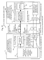
- Fig. 1 is a block diagram showing a configuration of a quantum communication system 100 of the present embodiment.
- the quantum communication system 100 (also referred to as “quantum encryption communication system”) includes a quantum encryption transmitting apparatus 200, a quantum encryption receiving apparatus 300, a quantum communication path 101 (also referred to as “quantum signal communication path”), a heralding signal communication path 102, and a clock communication path 103 (also referred to as “pulse clock communication path” or “pulse clock signal communication path”) that connect the two apparatuses.
- the quantum communication path 101 is a communication path that conveys a photon as a quantum signal.
- a dispersion compensation fiber 104 may be connected subsequently to it in order to compensate a collapse in an optical pulse waveform, which is associated with a wavelength dispersion peculiar to the optical fiber.
- the heralding signal communication path 102 is a communication path that conveys a heralding signal which will be described later.
- the clock communication path 103 is a communication path that conveys a clock signal (also referred to as "pulse clock signal”) which will be described later.
- the heralding signal communication path 102 and the clock communication path 103 may be optical communication paths or may be communication paths of electric signals.
- the quantum encryption transmitting apparatus 200 is one example of the quantum communication apparatus, and it includes a pulse-driven heralded single-photon source 201, a quantum signal modulating unit 203, a heralding signal transmitting unit 205, a clock signal transmitting unit 206, and a timing adjuster 202.
- the pulse-driven heralded single-photon source 201 is one example of a signal generating unit.
- the quantum signal modulating unit 203 includes a quantum signal modulator 204 which adds the signal modulation to a quantum state of a single photon output from the pulse-driven heralded single-photon source 201.
- the heralding signal transmitting unit 205 is a transceiver or a transmitter for transmitting the heralding signal output from the pulse-driven heralded single-photon source 201 to the heralding signal communication path 102.
- the clock signal transmitting unit 206 is a transceiver or a transmitter for transmitting the clock signal of a pulse laser serving as a pump source of the pulse-driven heralded single-photon source 201 to the clock communication path 103.
- the timing adjuster 202 is one example of a first timing adjusting unit and it generates a first trigger signal (also simply referred to as "trigger signal”) given to the quantum signal modulator 204 by synchronizing the heralding signal with the pulse clock signal.
- the heralding signal is a signal output at irregular intervals in synchronization with the single photon, which has a jitter in between itself and the single photon that cannot be ignored.
- the pulse clock signal is a clock signal of the pulse laser of the pump light source, it is output regularly even at a time slot where the single photon is not output. Note that a jitter in between the pulse clock signal and the single photon is extremely small. In case of using a femtosecond pulse laser as the pump light source, the jitter is 1 ps or less.
- the quantum encryption receiving apparatus 300 is one example of the quantum communication apparatus, and it includes a quantum signal detecting unit 304, a heralding signal receiving unit 301, a clock signal receiving unit 302, and a timing adjuster 303.
- the quantum signal detecting unit 304 includes a photon detector 306 for detecting a photon that is transferred through the quantum communication path 101, and a quantum signal demodulator 305 for performing a signal demodulation to the quantum state of the photon that is transferred through the quantum communication path 101.
- the quantum signal demodulator 305 is one example of a quantum signal demodulating unit.
- the heralding signal receiving unit 301 is a receiver or a transceiver for receiving the heralding signal that is transferred through the heralding signal communication path 102.
- the clock signal receiving unit 302 is a receiver or a transceiver for receiving the pulse clock signal that is transferred through the clock communication path 103.
- the timing adjuster 303 is one example of a second timing adjusting unit, and it synchronizes the heralding signal received at the heralding signal receiving unit 301 with the pulse clock signal received at the clock signal receiving unit 302, and generates a second trigger signal (also simply referred to as "trigger signal”) given to the photon detector 306 and the quantum signal demodulator 305.
- a high-speed operation with a low jitter is desired in a transmitter (i.e., the clock signal transmitting unit 206) and a receiver (i.e., the clock signal receiving unit 302) used for the clock communication path 103. Therefore, depending on the circumstances, a configuration of the clock communication path 103, in which a part of the pulse laser light output from the pump light source of the pulse-driven heralded single-photon source 201 is diverged, its wavelength is converted into a wavelength appropriate for the communication path if needed, and it is transferred by using an optical fiber, may be employed.
- a secure communication is realized by randomly selecting mutually conjugate measurement means.
- the quantum signal demodulator 305 is used in case of actively selecting the measurement means at the receiving side.
- the quantum signal demodulator 305 is used in case of passively selecting the measurement means.
- a configuration where the photon detectors 306 used for the measurement are increased instead of using the quantum signal demodulator 305, is employed.
- the former configuration is illustrated in Fig. 1 .
- the latter configuration is described in a third embodiment and onwards.
- Fig. 2 is a drawing showing one example of a quantum encryption optical system that actively selects a measurement means at the receiving side. For simplicity, a control system is omitted in Fig. 2.
- Fig. 2 illustrates one example of a configuration of the quantum signal modulating unit 203 and the quantum signal detecting unit 304, especially.
- the quantum state is actively specified and transmitted by using a phase modulator 208. Also in the quantum encryption receiving apparatus 300, the quantum state is actively measured by using a phase demodulator 307. Moreover, a non-symmetrical Mach-Zehnder interferometer 308 corresponding to previously set and fixed measurement means is placed next to the phase demodulator 307, and it leads to photon detectors 306a and 306b corresponding to the measurement means. In this example, in the quantum signal modulating unit 203 of the quantum encryption transmitting apparatus 200, a non-symmetrical Mach-Zehnder interferometer 207 is used before the phase modulator 208, in order to perform processing of the signal modulation.
- phase modulator 208 is used as one example of the quantum signal modulator 204, but a polarization modulator and the like may be used instead.
- phase demodulator 307 is used as one example of the quantum signal demodulating unit, but a polarization demodulator and the like may be used instead.
- an input device which is not illustrated inputs the 2-bit information to a processing device which is not illustrated.
- a storage device which is not illustrated may store this 2-bit information, and the processing device may read this 2-bit information from the storage device.
- the processing device converts the 2-bit information into an electric signal, and inputs it to the quantum signal modulating unit 203.
- the quantum signal modulating unit 203 implements the signal modulation to one photon of the photon pair output from the pulse-driven heralded single-photon source 201, based on the electric signal input from the processing device, by using the non-symmetrical Mach-Zehnder interferometer 207 and the phase demodulator 208.
- the phase modulator 208 performs a phase modulation of the photon at four kinds of phase differences ⁇ 0, ⁇ /2, ⁇ , (3/2) ⁇ . In this way, 2-bit signal modulation is implemented to that photon.
- the photon to which such a signal modulation has been implemented is transferred from the quantum encryption transmitting apparatus 200 to the quantum encryption receiving apparatus 300, via the quantum communication path 101.
- the quantum signal detecting unit 304 In the quantum encryption receiving apparatus 300, the quantum signal detecting unit 304 generates a 1-bit random number by using a random number generator which is not illustrated, and inputs the generated 1-bit random number to the phase demodulator 307.
- the quantum signal detecting unit 304 implements the signal demodulation to the photon transferred through the quantum communication path 101, based on an electric signal of the inputted 1-bit random number, by using the phase demodulator 307.
- the phase demodulator 307 performs 0 or ⁇ /2 phase modulation (i.e., the phase demodulation) of a photon depending on a value of the 1-bit random number (e.g., if the value of the 1-bit random number is "1," ⁇ /2 phase modulation is performed).
- the photon detector 306a and the photon detector 306b are connected to the phase demodulator 307 via the non-symmetrical Mach-Zehnder interferometer 308.
- the quantum signal detecting unit 304 specifies a value of one bit of the 2-bit information, depending on whether the photon detector 306a or the photon detector 306b has detected the photon to which the signal demodulation has been implemented. The bit specified here becomes valid if the remaining one bit of the 2-bit information carries the same value as the 1-bit random number.
- the photon detector 306a may detect a photon having a phase difference of 0, and the photon detector 306b may detect a photon having a phase difference of ⁇ .
- phase difference of the photon transferred through the quantum communication path 101 is either 0 or ⁇ and the phase demodulator 307 carries out 0 phase modulation (i.e., does not carry out phase modulation), a bit specified by the quantum signal detecting unit 304 becomes valid.
- phase difference of the photon transferred through the quantum communication path 101 is either ⁇ /2 or (3/2) ⁇ and the phase demodulator 307 carries out ⁇ /2 phase demodulation, a bit specified by the quantum signal detecting unit 304 becomes valid.
- An output device which is not illustrated outputs the bit specified by the quantum signal detecting unit 304.
- the processing device which is not illustrated may carry out a predetermined processing by using this bit. This bit, for example, can be utilized as key information or a part of key information.
- Fig. 3 is a timing chart illustrating one example of the quantum encryption communication of the present embodiment.
- pulse clock signals (“transmitting side clock signals”) are regularly output from the pulse-driven heralded single-photon source 201 included in the quantum encryption transmitting apparatus 200.
- generation of a single photon occurs probabilistically, and thus outputs of the single photon and the heralding signal ("transmitting side heralding signal") associated with it occur irregularly.
- a timing of the generation of the single photon is synchronous with the pulse clock signal very precisely.
- the heralding signal has a jitter in 500-ps units.
- the timing adjuster 202 included in the quantum encryption transmitting apparatus 200 takes in the heralding signal and the pulse clock signal, and it outputs a first trigger signal ("quantum signal modulation trigger signal") precisely synchronous to the pulse clock signal, only when the heralding signal is input, and operates the quantum signal modulator 204. In this way, the single photon output from the pulse-driven heralded single-photon source 201 precisely receives the signal modulation.
- the pulse clock signal and the heralding signal are transferred to the quantum encryption receiving apparatus 300 via the clock communication path 103 and the heralding signal communication path 102, respectively.
- the single photon that received the signal modulation is transferred to the quantum encryption receiving apparatus 300 via the quantum communication path 101.
- the pulse clock signal (“receiving side clock signal”) and the heralding signal (“receiving side heralding signal”) transferred to the quantum encryption receiving apparatus 300 are received at the clock signal receiving unit 302 and the heralding signal receiving unit 301, respectively, and are input to the timing adjuster 303 included in the quantum encryption receiving apparatus 300.
- the timing adjuster 303 outputs a second trigger signal ("a photon detecting trigger signal”) precisely synchronous to the pulse clock signal, only when the heralding signal is input, and operates the photon detector 306.
- a timing of inputting the single photon transferred to the quantum encryption receiving apparatus 300 into the photon detector 306 and an operation timing of the photon detector 306, are precisely synchronous at a low jitter, and thereby a stable and highly-efficient photon detection is possible.
- the timing adjuster 303 outputs a second trigger signal (a quantum signal demodulation trigger signal) precisely synchronous to the pulse clock signal, only when the heralding signal is input, in the same manner as the second trigger signal for the photon detector 306, and operates the quantum signal demodulator 305. In this way, a signal demodulation operation can be implemented in precise synchronization with the single photon transferred to the quantum encryption receiving apparatus 300.
- a second trigger signal a quantum signal demodulation trigger signal
- a clock frequency of the pulse clock signal is set to 80 MHz
- an unit time of the clock is 12.5 ns.
- the heralding signal can be synchronized to the pulse clock signal.
- the jitter of the heralding signal is about 500 ps and, therefore, it is sufficiently possible to synchronize the heralding signal with the pulse clock signal.
- the jitter of the pulse clock signal can be suppressed to about 1 ps, it is possible to suppress the jitter of the trigger signal generated by synchronizing the heralding signal with the pulse clock signal to about 100 ps. In this way, it becomes possible to reduce an influence of the performance of the photon detector 306 on stability and efficiency of the quantum communication.
- a timing of the quantum signal modulation of the quantum encryption transmitting apparatus 200, a timing of the quantum signal demodulation of the quantum encryption receiving apparatus 300, and a timing of the photon detection are synchronized not only with the heralding signal having a jitter that cannot be ignored against a transfer timing of the single photon, but also with the pulse clock signal having an extremely small jitter against the transfer timing of the single photon. Therefore, for each single photon transferred, respective operations of the quantum signal modulation, the quantum signal demodulation, and the photon detection can be stabilized and implemented at high efficiency.
- the single photon is generated probabilistically and irregularly, it is generated in precise synchronization with the pulse clock signal which is output regularly. Therefore, two photon measurement such as a Bell measurement with a photon generated from another photon source can be realized easily.
- the quantum communication system 100 of the present embodiment is a preferred system in using the quantum repeater and the quantum relay, making it capable of remarkably extending the communication distance.
- Fig. 4 is a drawing showing one example of a hardware resource of the quantum communication apparatus (i.e., the quantum encryption transmitting apparatus 200 or the quantum encryption receiving apparatus 300) of the present embodiment.
- the quantum communication apparatus is a computer that includes the hardware resource such as a display apparatus 901 having a display screen such as a CRT (Cathode Ray Tube) and a LCD (Liquid Crystal Display), a keyboard 902 (K/B), a mouse 903, a FDD 904 (Flexible Disk Drive), a CDD 905 (Compact Disc Drive), and a printer apparatus 906, which are connected by cables or signal lines. Moreover, it is connected to the Internet via a LAN (Local Area Network) and a gateway.
- a display apparatus 901 having a display screen such as a CRT (Cathode Ray Tube) and a LCD (Liquid Crystal Display), a keyboard 902 (K/B), a mouse 903, a FDD 904 (Flexible Disk Drive), a CDD 905 (Compact Disc Drive), and a printer apparatus 906, which are connected by cables or signal lines.
- a printer apparatus 906 which are connected by cables or signal lines.
- the quantum communication apparatus includes a CPU 911 (Central Processing Unit) for executing programs.
- the CPU 911 is one example of the processing device.
- the CPU 911 is connected to a ROM 913 (Read Only Memory), a RAM 914 (Random Access Memory), a communication board 915, the display apparatus 901, the keyboard 902, the mouse 903, the FDD 904, the CDD 905, the printer apparatus 906, and a magnetic disk apparatus 920, via a bus 912, and controls these hardware devices.
- a storage medium such as an optical disk apparatus and a memory card reader/writer may be used.
- Example of a volatile memory includes the RAM 914.
- Examples of a non-volatile memory include the storage media such as the ROM 913, the FDD 904, the CDD 905 and the magnetic disk apparatus 920. These are examples of storage devices.
- Examples of the input device include the communication board 915, the keyboard 902, and the FDD 904.
- examples of the output device include the communication board 915, the display apparatus 901, and the printer apparatus 906.
- the communication board 915 is connected to the LAN and the like.
- the communication board 915 may also be connected to the Internet, or a WAN (Wide Area Network) such as an ISDN (Integrated Services Digital Network).
- the gateway is not needed in case of being connected to the Internet or the WAN.
- the magnetic disk apparatus 920 stores an operating system 921 (OS), programs 923, and files 924.
- a program of the programs 923 is executed by the CPU 911 and the operating system 921.
- the programs 923 store programs that process data or information.
- the programs are read and executed by the CPU 911.
- the files 924 store data, information, signal values, variable values or parameters, which are described as “... data”, “information”, “ ... ID (IDentifier)", “... flag”, “... result” in the description of the present embodiment, as each item of "... file,” “... database” or “...table.” "...file,” “...database” or “...table” are stored on the storage medium such as disk or memory.
- the data, information, signal values, variable values or parameters stored on the storage media such as disk or memory are read to a main memory or a cash memory by the CPU 911 via a read-write circuit, to be used in processes (operations) of the CPU 911 such as extracting, searching, referring, comparing, operating, calculating, controlling, outputing, printing, displaying and so forth on.
- processes (operations) of the CPU 911 such as extracting, searching, referring, comparing, operating, calculating, controlling, outputing, printing, displaying and so forth on.
- the data, information, signal values, variable values or parameters are temporarily stored on the main memory, the cash memory or a buffer memory.
- those elements being described as “... unit” and “...means” in the description of the present embodiment can also be “...circuit,” “...apparatus” and “...equipment”, and it can also be “ ... step,” “...process,” “...procedure” and “...processing.”
- those elements described as “... unit” or “... means” may be implemented as a firmware stored on the ROM 913.
- they may be implemented as a combination of the software and the hardware such as elements, devices, substrates and wirings, or a combination further with the firmware.
- Firmware and software are stored on the storage media such as magnetic disk, flexible disk, optical disk, compact disc, mini disk, and DVD as programs. These programs are read by the CPU 911, and executed by the CPU 911.
- Fig. 5 is a flow chart showing a quantum communication method of the transmitting side in which the quantum encryption transmitting apparatus 200 transmits the photon output as the quantum signal from the single-photon source where the photon is output by pulse driving, via the quantum communication path 101.
- the pulse-driven heralded single-photon source 201 generates the photon pair by the parametric down conversion and the like, and outputs one photon of the photon pair as the quantum signal, and also outputs the other photon of the photon pair as the heralding signal (step S101).
- the timing adjuster 202 outputs as the first trigger signal, the heralding signal indicating a presence of the quantum signal output from the pulse-driven heralded single-photon source 201 on the quantum communication path 101 in synchronization with the clock signal for pulse driving the pulse-driven heralded single-photon source 201 (step S102).
- the quantum signal modulating unit 203 implements the signal modulation to the quantum signal output from the pulse-driven heralded single-photon source 201, in timing with the first trigger signal output from the timing adjuster 202 (step S103), and transmits the quantum signal to which the signal modulation has been implemented, via the quantum communication path 101 (step S104).
- the heralding signal transmitting unit 205 transmits the heralding signal output from the pulse-driven heralded single-photon source 201 via the heralding signal communication path 102 (step S105).
- the clock signal transmitting unit 206 transmits the clock signal via the clock communication path 103 (step S106).
- Fig. 6 is a flow chart showing a quantum communication method of the receiving side in which the quantum encryption receiving apparatus 300 receives the photon output as the quantum signal from the single-photon source (i.e., the pulse-driven heralded single-photon source 201 included in the quantum encryption transmitting apparatus 200) that outputs the photon by pulse driving from the quantum encryption transmitting apparatus 200, via the quantum communication path 101.
- the single-photon source i.e., the pulse-driven heralded single-photon source 201 included in the quantum encryption transmitting apparatus 200
- the heralding signal receiving unit 301 receives a heralding signal indicating the presence of the quantum signal output from the single-photon source on the quantum communication path 101, from the quantum encryption transmitting apparatus 200, via the heralding signal communication path 102 (step S201).
- the clock signal receiving unit 302 receives the clock signal for pulse driving the single-photon source, from the quantum encryption transmitting apparatus 200, via the clock communication path 103 (step S202).
- the timing adjuster 303 outputs as the second trigger signal, the heralding signal received by the heralding signal receiving unit 301 in synchronization with the clock signal received at the clock signal receiving unit 302 (step S203).
- the quantum signal demodulator 305 included in the quantum signal detecting unit 304 implements the signal demodulation to the quantum signal present on the quantum communication path 101, in timing with the second trigger signal output from the timing adjuster 303 (step S204).
- the quantum signal detecting unit 304 detects the quantum signal to which the signal demodulation has been implemented by the quantum signal demodulator 305, in timing with the second trigger signal output from the timing adjuster 303 (step S205).
- the quantum communication system 100 that performs the quantum encryption communication by using the pulse-driven heralded single-photon source 201 which outputs the heralding signal generated by the parametric down conversion and the like, is characterized in that, as well as the quantum communication path 101, the heralding signal communication path 102, and other communication paths for transferring control signals, the clock communication path 103 for transferring the clock signal of the pulse laser used as the pump source for the parametric down conversion and the like, from the quantum encryption transmitting apparatus 200 to the quantum encryption receiving apparatus 300, are provided.
- the quantum encryption transmitting apparatus 200 is characterized in that the pulse-driven heralded single-photon source 201, the quantum signal modulator 204 that adds the signal modulation to the quantum state of the single photon, the heralding signal transmitting unit 205 that transmits the heralding signal output from the pulse-driven heralded single-photon source 201 to the heralding signal communication path 102, the clock signal transmitting unit 206 that transmits the pulse clock signal output from the pulse-driven heralded single-photon source 201 to the clock communication path 103, and the timing adjuster 202 that generates the trigger signal to the quantum signal modulator 204 by synchronizing, with a high precision, the heralding signal to the pulse clock signal, are provided.
- the quantum encryption receiving apparatus 300 is characterized in that the photon detector 306 that detects a photon transferred through the quantum communication path 101, the heralding signal receiving unit 301 that receives the heralding signal transferred through the heralding signal communication path 102, the clock signal receiving unit 302 that receives the pulse clock signal transferred through the clock communication path 103, and the timing adjuster 303 that generates the trigger signal to the photon detector 306 by synchronizing, with a high precision, the heralding signal to the pulse clock signal, are provided.
- the quantum encryption receiving apparatus 300 is characterized in that the quantum signal demodulator 305 that implements the signal demodulation to the photon propagating through the quantum communication path 101, and the timing adjuster 303 that generates the trigger signal to the quantum signal modulator 305 by synchronizing, with a high precision, the heralding signal to the pulse clock signal, are provided.
- the quantum communication system 100 is characterized in that the dispersion compensation fiber 104 is used subsequently to the optical fiber serving as the quantum communication path 101.
- the quantum communication apparatus of the present embodiment a stable and highly-efficient quantum communication can be realized without being influenced by the jitter of the heralding signal.
- the quantum communication apparatus of the receiving side employs a configuration having a small number of photon detectors and, therefore, the configuration becomes relatively compact. The cost also becomes relatively low.
- the present embodiment mainly differences from the first embodiment, will be described.
- the first embodiment employs the configuration in which the pulse laser serving as the pump light source of the pulse-driven heralded single-photon source 201 is used as a master clock.
- a clock is shared at a low jitter in between the two quantum encryption communication apparatuses, and the pulse laser serving as the pump light source is synchronized and driven by using the shared clock as a master.
- the clock signal that synchronizes the heralding signal for generating the trigger signal is transmitted from the quantum encryption transmitting apparatus 200 to the quantum encryption receiving apparatus 300.
- it is transmitted from the quantum encryption receiving apparatus 300 to the quantum encryption transmitting apparatus 200.
- Fig. 7 is a block diagram showing a configuration of the quantum communication system 100 of the present embodiment.
- the quantum encryption transmitting apparatus 200 includes a clock signal receiving unit 209 in place of the clock signal transmitting unit 206
- the quantum encryption transmitting apparatus 300 includes a clock signal transmitting unit 309 in place of the clock signal receiving unit 302.
- the clock signal transmitting unit 309 is a transceiver or a transmitter for transmitting a clock signal generated by a built-in clock in the timing modulator 303 to the clock communication path 103.
- the timing adjuster 303 synchronizes a heralding signal received by the heralding signal receiving unit 301 with the clock signal generated by a built-in clock in itself, and generates a second trigger signal given to the photon detector 306 and the quantum signal demodulator 305.
- the clock signal receiving unit 209 is a receiver or a transceiver for receiving the clock signal transferred through the clock communication path 103.
- the timing adjuster 202 synchronizes the heralding signal output from the pulse-driven heralded single-photon source 201 with the clock signal received at the clock signal receiving unit 209, and generates a first trigger signal given to the quantum signal modulator 204.
- Fig. 8 is a flow chart illustrating the quantum communication method of the transmitting side.
- the clock signal receiving unit 209 receives the clock signal for pulse driving the pulse-driven heralded single-photon source 201, from the quantum encryption receiving apparatus 300, via the clock communication path 103 (step S111).
- the pulse-driven heralded single-photon source 201 is driven in synchronization with the clock signal received by the clock signal receiving unit 209, and generates the photon pair by the parametric down conversion and the like (step S 112). Then, it outputs one photon of the photon pair as the quantum signal, and outputs the other photon of the photon pair as the heralding signal.
- the timing adjuster 202 outputs as a first trigger signal, a heralding signal indicating a presence of the quantum signal output from the pulse-driven heralded single-photon source 201 on the quantum communication path 101 in synchronization with the clock signal received at the clock signal receiving unit 209 (step S113).
- the quantum signal modulating unit 203 implements a signal modulation to the quantum signal output from the pulse-driven heralded single-photon source 201, in timing with the first trigger signal output from the timing adjuster 202 (step S 114), and transmits the quantum signal to which the signal modulation has been implemented via the quantum communication path 101 (step S 115).
- the heralding signal transmitting unit 205 transmits the heralding signal output from the pulse-driven heralded single-photon source 201, via the heralding signal communication path 102 (step S 116).
- Fig. 9 is a flow chart illustrating the quantum communication method of the receiving side.
- the clock signal transmitting unit 309 transmits the clock signal for pulse driving the single-photon source, via the clock communication path 103 (step S211).
- the heralding signal receiving unit 301 receives the heralding signal indicating the presence of the quantum signal output from the single-photon source on the quantum communication path 101, from the quantum encryption transmitting apparatus 200, via the heralding signal communication path 102 (step S212).
- the timing adjuster 303 outputs as the second trigger signal, the heralding signal received at the heralding signal receiving unit 301 in synchronization with the clock signal (step S213).
- the quantum signal demodulator 305 included in the quantum signal detecting unit 304 implements the signal demodulation to the quantum signal which is present on the quantum communication path 101, in timing with the second trigger signal output from the timing adjuster 303 (step S214).
- the quantum signal detecting unit 304 detects the quantum signal to which the signal demodulation has been implemented by the quantum signal demodulator 305, in timing with the second trigger signal output from the timing adjuster 303 (step S215).
- a stable and highly-efficient quantum communication can be realized without being influenced by the jitter of the heralding signal.
- a supply source of the clock signal used for that purpose can be installed somewhere other than the quantum communication apparatus of the transmitting side.
- the present embodiment mainly differences from the first embodiment, will be described.
- the first embodiment employs the configuration in which, in the quantum signal detecting unit 304 of the quantum encryption receiving apparatus 300, the quantum signal demodulator 305 is used, and the measurement means of the quantum state of the photon transmitted from the quantum encryption transmitting apparatus 200 is selected actively.
- the present embodiment employs a configuration in which, instead of using the quantum signal demodulator 305, the photon detectors 306 used for the measurement are increased, and the measurement means of the quantum state is selected passively.
- Fig. 10 is a block diagram showing a configuration of the quantum communication system 100 of the present embodiment.
- the main difference from Fig. 1 described in the first embodiment resides in that the quantum signal detecting unit 304 of the quantum encryption receiving apparatus 300 includes a beam splitter 310 in place of the quantum signal demodulator 305.
- the beam splitter 310 passively and randomly selects an optical path of the photon which is transferred from the quantum encryption transmitting apparatus 200, via the quantum communication path 101.
- the photon detector 306 detects a photon on the optical path selected by the beam splitter 310. Since the quantum signal detecting unit 304 does not include the quantum signal demodulator 305, the timing adjuster 303 need give a second trigger signal only to the photon detector 306.
- Fig. 11 is a drawing showing one example of the quantum encryption optical system that passively selects a measurement means at the receiving side.
- the control system is omitted in Fig. 11.
- Fig. 11 illustrates one example of a configuration of the quantum signal modulating unit 203 and the quantum signal detecting unit 304, especially.
- the quantum state is actively specified and transmitted by using the phase modulator 208.
- the optical path is passively and randomly selected at the beam splitter 310.
- the non-symmetrical Mach-Zehnder interferometer 207 is used before the phase modulator 208.
- the phase modulator 208 is used as one example of the quantum signal modulator 204, but the polarization modulator and the like may be used instead.
- the beam splitter 310 is used as one example of a quantum signal diverging unit.
- the input device which is not illustrated inputs the 2-bit information to the processing device which is not illustrated.
- the storage device which is not illustrated may store this 2-bit information, and the processing device may read this 2-bit information from the storage device.
- the processing device converts the 2-bit information into the electric signal, and inputs it to the quantum signal modulating unit 203.
- the quantum signal modulating unit 203 implements the signal modulation to one photon of the photon pair output from the pulse-driven heralded single-photon source 201, based on the electric signal input from the processing device, by using the non-symmetrical Mach-Zehnder interferometer 207 and the phase demodulator 208.
- the phase demodulator 208 performs the phase modulation of the photon at four kinds of phase differences ⁇ 0, ⁇ /2, ⁇ , (3/2) ⁇ . In this way, 2-bit signal modulation is implemented to that photon.
- the photon to which such a signal modulation has been implemented is transferred from the quantum encryption transmitting apparatus 200 to the quantum encryption receiving apparatus 300, via the quantum communication path 101.
- the quantum signal detecting unit 304 diverges the optical path of the photon transferred through the quantum communication path 101 into two optical paths by the beam splitter 310.
- the beam splitter 310 is a 50-50 nonpolarization beam splitter.
- One of the optical paths diverged by this beam splitter 310 is connected with the photon detector 306a and the photon detector 306b via the non-symmetrical Mach-Zehnder interferometer 308a.
- the other one of the optical paths is connected with the photon detector 306c and the photon detector 306d via the non-symmetrical Mach-Zehnder interferometer 308a.
- the quantum signal detecting unit 304 specifies values of two bits of the 2-bit information, depending on which of the photon detectors 306a to 306d has detected the photon transferred through the quantum communication path 101.
- One bit of the two bits specified here becomes valid if an optical path corresponding to a value of the remaining one bit and an optical path selected at the beam splitter 310 coincides.
- the non-symmetrical Mach-Zehnder interferometer 308a may be set up to output a photon having a phase difference of 0 or ⁇
- the non-symmetrical Mach-Zehnder interferometer 308b may be set up to output a photon having a phase difference of ⁇ /2 or (3/2) ⁇ .
- the photon detector 306a may detect a photon having a phase difference of 0, the photon detector 306b may detect a photon having a phase difference of ⁇ , the photon detector 306c may detect a photon having a phase difference of ⁇ /2, and the photon detector 306d may detect a photon having a phase difference of (3/2) ⁇ .
- the phase difference of the photon transferred through the quantum communication path 101 is either 0 or ⁇
- the beam splitter 310 selects an optical path to which the non-symmetrical Mach-Zehnder interferometer 308a is connected, a bit specified by the quantum signal detecting unit 304 becomes valid.
- the beam splitter 310 selects an optical path to which the non-symmetrical Mach-Zehnder interferometer 308b is connected, a bit specified by the quantum signal detecting unit 304 becomes valid.
- the output device which is not illustrated outputs the bit specified by the quantum signal detecting unit 304.
- the processing device which is not illustrated may carry out a predetermined processing by using this bit. This bit, for example, can be utilized as key information or a part of key information.
- Fig. 12 is a timing chart illustrating one example of the quantum encryption communication of the present embodiment.
- Fig. 12 is similar to Fig. 3 described in the first embodiment, except that the second trigger signal ("quantum signal demodulation trigger signal") for operating the quantum signal demodulator 305 at the receiving side is not needed.
- Fig. 13 is a flow chart illustrating the quantum communication method of the receiving side.
- the quantum communication method of the transmitting side is similar to that shown in Fig. 5 of the first embodiment.
- the heralding signal receiving unit 301 receives the heralding signal indicating the presence of the quantum signal output from the single-photon source on the quantum communication path 101, from the quantum encryption transmitting apparatus 200, via the heralding signal communication path 102 (step S221).
- the clock signal receiving unit 302 receives the clock signal for pulse driving the single-photon source, from the quantum encryption transmitting apparatus 200, via the clock communication path 103 (step S222).
- the timing adjuster 303 outputs as the second trigger signal, the heralding signal received at the heralding signal receiving unit 301 in synchronization with the clock signal received at the clock signal receiving unit 302 (step S223).
- a beam splitter 310 included in the quantum signal detecting unit 304 diverges the quantum communication path 101 (step S224).
- the quantum signal detecting unit 304 detects the quantum signal which is present on the quantum communication path 101 diverged by the beam splitter 310, in timing with the second trigger signal output from the timing adjuster 303 (step S225).
- the quantum communication apparatus of the present embodiment by using the quantum communication apparatus of the present embodiment, a stable and highly-efficient quantum communication can be realized without being influenced by the jitter of the heralding signal. Moreover, as for the quantum communication apparatus of the receiving side, since it employs the configuration that does not use the quantum signal demodulator, the trigger signal given to the quantum signal demodulator is not needed, and a control becomes relatively easy.
- the clock signal which synchronizes the heralding signal for generating the trigger signal is transmitted from the quantum encryption transmitting apparatus 200 to the quantum encryption receiving apparatus 300.
- it is transmitted from the quantum encryption receiving apparatus 300 to the quantum encryption transmitting apparatus 200.
- Fig. 14 is a block diagram showing a configuration of the quantum communication system 100 of the present embodiment.
- the main difference from Fig. 10 of the third embodiment resides in that the quantum encryption transmitting apparatus 200 includes the clock signal receiving unit 209 in place of the clock signal transmitting unit 206, and that the quantum encryption receiving apparatus 300 includes a clock signal transmitting unit 309 in place of the clock signal receiving unit 302. Function of the clock signal transmitting unit 309 and the clock signal receiving unit 209 is similar to that illustrated in Fig. 7 of the second embodiment.
- Fig. 15 is a flow chart illustrating a quantum communication method of the receiving side.
- the quantum communication method of the transmitting side is similar to that illustrated in Fig. 8 of the second embodiment.
- the clock signal transmitting unit 309 transmits the clock signal for pulse driving the single-photon source, via the clock communication path 103 (step S231).
- the heralding signal receiving unit 301 receives the heralding signal indicating the presence of the quantum signal output from the single-photon source on the quantum communication path 101, from the quantum encryption transmitting apparatus 200, via the heralding signal communication path 102 (step S232).
- the timing adjuster 303 outputs as the second trigger signal, the heralding signal received by the heralding signal receiving unit 301 in synchronization with the clock signal (step S233).
- the beam splitter 310 included in the quantum signal detecting unit 304 diverges the quantum communication path 101 (step S234).
- the quantum signal detecting unit 304 detects the quantum signal present on the quantum communication path 101 which is diverged by the beam splitter 310, in timing with the second trigger signal output from the timing adjuster 303 (step S235).
- a stable and highly-efficient quantum communication can be realized.
- a supply source of the clock signal used for that purpose can be installed somewhere other than the quantum communication apparatus of the transmitting side.
- the present embodiment mainly differences from the first embodiment, will be described.
- the heralding signal output from the pulse-driven heralded single-photon source 201 is used as it is, as the heralding signal.
- the heralding signal output from the pulse-driven heralded single-photon source 201 and the pulse clock signal output from the same are input into an AND operation gate, and a signal output from the gate is used as the heralding signal.
- Fig. 16 is a block diagram showing a configuration of the quantum communication system 100 of the present embodiment.
- the quantum encryption transmitting unit 200 includes not only the pulse-driven heralded single-photon source 201 but also an AND gate 210 (a logical AND operation gate) as the signal generating unit.
- the signal generating unit generates the photon pair with the pulse-driven heralded single-photon source 201, and outputs one photon of the photon pair as the quantum signal.
- the signal generating unit also performs a logical AND operation of the other photon of the photon pair (i.e., the heralding signal) and the clock signal with the AND gate 210, and outputs a result of the logical AND operation as a new heralding signal.
- the AND gate 210 performs the logical AND operation of the heralding signal and the pulse clock signal, and its result is set as a heralding signal once again.
- an influence due to the error of such heralding signal can be restricted to a timing of the pulse clock signal. That is, by using the quantum communication apparatus of the present embodiment, the influence due to the error of the heralding signal can be reduced. As a result, S/N ratio (signal-to-noise ratio) becomes high.
- the differences between the first embodiment and the present embodiment can also be applied to the second to fourth embodiments. That is, in the second to fourth embodiments, in the quantum encryption transmitting apparatus 200, the heralding signal output from the pulse-driven heralded single-photon source 201 is used as it is, as the heralding signal. However, in the second to fourth embodiments, similar to the present embodiment, the heralding signal output from the pulse-driven heralded single-photon source 201 and the clock signal output from the same (alternatively, received from the quantum encryption receiving apparatus 300) are input into the logical AND operation gate, and a signal output from the gate may be used as the heralding signal.
- the logical AND operation of the heralding signal and the pulse clock signal output from the pulse-driven heralded single-photon source 201 is performed by using the AND gate 210, so that the heralding signal is output (from the signal generating unit) only at a rising edge of the pulse clock signal.
- the influence due to the error of the heralding signal can be restricted to the timing of the pulse clock signal.
- the signal generating unit may perform the logical AND operation of the heralding signal and the pulse clock signal by using a means other than the AND gate 210, and output a result of the AND operation as a heralding signal once again.
- the signal generating unit may use a method other than the logical AND operation (e.g., logical NOR operation, logical NAND operation, logical OR operation, or an arbitrary combination of these), to control the heralding signal with the pulse clock signal, and output a controlled heralding signal.
- each quantum communication apparatus may include both configurations of the transmitting side and the receiving side.
- 100 quantum communication system; 101: quantum communication path; 102: heralding signal communication path; 103: clock communication path; 104: dispersion compensation fiber; 200: quantum encryption transmitting apparatus; 201: pulse-driven heralded single-photon source; 202: timing adjuster; 203: quantum signal modulating unit; 204: quantum communication modulator; 205: heralding signal transmitting unit; 206: clock signal transmitting unit; 207: non-symmetrical Mach-Zehnder interferometer; 208: phase modulator; 209: clock signal receiving unit; 210: AND gate; 300: quantum encryption receiving apparatus; 301: heralding signal receiving unit; 302: clock signal receiving unit; 303: timing adjuster; 304: quantum signal detecting unit; 305: quantum signal demodulator; 306: photon detector; 307: phase modulator; 308: non-symmetrical Mach-Zehnder interferometer; 309: clock signal transmitting unit; 310: beam splitter; 901: display apparatus; 902:
Applications Claiming Priority (1)
| Application Number | Priority Date | Filing Date | Title |
|---|---|---|---|
| PCT/JP2006/315490 WO2008015758A1 (fr) | 2006-08-04 | 2006-08-04 | Appareil, système et procédé de communication quantique |
Publications (3)
| Publication Number | Publication Date |
|---|---|
| EP2051411A1 true EP2051411A1 (de) | 2009-04-22 |
| EP2051411A4 EP2051411A4 (de) | 2010-11-24 |
| EP2051411B1 EP2051411B1 (de) | 2012-03-07 |
Family
ID=38996946
Family Applications (1)
| Application Number | Title | Priority Date | Filing Date |
|---|---|---|---|
| EP06782348A Not-in-force EP2051411B1 (de) | 2006-08-04 | 2006-08-04 | Vorrichtung, system und verfahren zur quantenkommunikation |
Country Status (4)
| Country | Link |
|---|---|
| US (1) | US8270841B2 (de) |
| EP (1) | EP2051411B1 (de) |
| JP (1) | JP4775919B2 (de) |
| WO (1) | WO2008015758A1 (de) |
Cited By (1)
| Publication number | Priority date | Publication date | Assignee | Title |
|---|---|---|---|---|
| US11588613B1 (en) | 2021-10-26 | 2023-02-21 | Eagle Technology, Llc | Systems and methods for synchronization of photons over quantum channels with co-propagating clock pulses |
Families Citing this family (49)
| Publication number | Priority date | Publication date | Assignee | Title |
|---|---|---|---|---|
| JP5019979B2 (ja) * | 2007-07-05 | 2012-09-05 | 三菱電機株式会社 | 量子暗号受信装置およびそれを使用する量子暗号受信方法 |
| GB0801408D0 (en) * | 2008-01-25 | 2008-03-05 | Qinetiq Ltd | Multi-community network with quantum key distribution |
| GB0801395D0 (en) * | 2008-01-25 | 2008-03-05 | Qinetiq Ltd | Network having quantum key distribution |
| US8855316B2 (en) * | 2008-01-25 | 2014-10-07 | Qinetiq Limited | Quantum cryptography apparatus |
| GB0801492D0 (en) * | 2008-01-28 | 2008-03-05 | Qinetiq Ltd | Optical transmitters and receivers for quantum key distribution |
| GB0809038D0 (en) * | 2008-05-19 | 2008-06-25 | Qinetiq Ltd | Quantum key device |
| GB0809045D0 (en) * | 2008-05-19 | 2008-06-25 | Qinetiq Ltd | Quantum key distribution involving moveable key device |
| GB0809044D0 (en) * | 2008-05-19 | 2008-06-25 | Qinetiq Ltd | Multiplexed QKD |
| GB0819665D0 (en) * | 2008-10-27 | 2008-12-03 | Qinetiq Ltd | Quantum key dsitribution |
| GB0822253D0 (en) * | 2008-12-05 | 2009-01-14 | Qinetiq Ltd | Method of establishing a quantum key for use between network nodes |
| GB0822254D0 (en) * | 2008-12-05 | 2009-01-14 | Qinetiq Ltd | Method of performing authentication between network nodes |
| GB0822356D0 (en) * | 2008-12-08 | 2009-01-14 | Qinetiq Ltd | Non-linear optical device |
| GB2470069A (en) * | 2009-05-08 | 2010-11-10 | Hewlett Packard Development Co | Quantum Repeater and System and Method for Creating Extended Entanglements |
| GB2471471A (en) * | 2009-06-30 | 2011-01-05 | Hewlett Packard Development Co | Quantum repeater and method for creating extended entanglements utilising triggering control signals from neighbouring repeater relay nodes |
| GB2471470A (en) * | 2009-06-30 | 2011-01-05 | Hewlett Packard Development Co | Quantum repeater and system and method for creating extended entanglements utilising cyclic synchronised control signals at repeater relay nodes |
| WO2011028857A2 (en) * | 2009-09-04 | 2011-03-10 | Telcordia Technologies, Inc. | High-probability heralded single-photon source and related method |
| GB0917060D0 (en) | 2009-09-29 | 2009-11-11 | Qinetiq Ltd | Methods and apparatus for use in quantum key distribution |
| US8483394B2 (en) | 2010-06-15 | 2013-07-09 | Los Alamos National Security, Llc | Secure multi-party communication with quantum key distribution managed by trusted authority |
| US9002009B2 (en) | 2010-06-15 | 2015-04-07 | Los Alamos National Security, Llc | Quantum key distribution using card, base station and trusted authority |
| JP5488342B2 (ja) * | 2010-08-27 | 2014-05-14 | 沖電気工業株式会社 | 量子相関光子対発生方法及び量子相関光子対発生装置 |
| JP5541004B2 (ja) * | 2010-08-27 | 2014-07-09 | 沖電気工業株式会社 | 量子鍵配送方法及び量子鍵配送システム |
| GB201020424D0 (en) | 2010-12-02 | 2011-01-19 | Qinetiq Ltd | Quantum key distribution |
| US9866379B2 (en) | 2011-09-30 | 2018-01-09 | Los Alamos National Security, Llc | Polarization tracking system for free-space optical communication, including quantum communication |
| FR2980933B1 (fr) * | 2011-09-30 | 2016-12-23 | Centre Nat De La Rech Scient - Cnrs | Methode et dispositif de synchronisation de sources d'intrication pour reseau de communication quantique |
| US9287994B2 (en) | 2011-09-30 | 2016-03-15 | Los Alamos National Security, Llc | Great circle solution to polarization-based quantum communication (QC) in optical fiber |
| US9509506B2 (en) | 2011-09-30 | 2016-11-29 | Los Alamos National Security, Llc | Quantum key management |
| CN102739394B (zh) * | 2012-06-07 | 2013-11-06 | 中国科学技术大学 | 光量子相位调制系统 |
| ES2717708T3 (es) | 2012-08-17 | 2019-06-24 | Triad Nat Security Llc | Sistema de comunicaciones cuánticas con dispositivos fotónicos integrados |
| US8842987B2 (en) * | 2012-10-03 | 2014-09-23 | Fmr Llc | Security in multiwavelength optical networks |
| US9258114B2 (en) * | 2012-12-05 | 2016-02-09 | Intel Corporation | Quantum key distribution (QSD) scheme using photonic integrated circuit (PIC) |
| JP6181434B2 (ja) * | 2013-06-11 | 2017-08-16 | 日本電信電話株式会社 | 量子中継ネットワークシステム |
| US10044504B2 (en) * | 2013-07-16 | 2018-08-07 | Los Alamos National Security, Llc | Long-haul high rate quantum key distribution |
| KR101610747B1 (ko) * | 2014-08-19 | 2016-04-08 | 한국과학기술연구원 | 양자 암호 통신 장치 및 방법 |
| US10056983B2 (en) | 2014-11-24 | 2018-08-21 | New York University | Quantum-assisted load balancing in communication-constrained wide-area physical networks |
| CN105871538B (zh) | 2015-01-22 | 2019-04-12 | 阿里巴巴集团控股有限公司 | 量子密钥分发系统、量子密钥分发方法及装置 |
| CN105991285B (zh) | 2015-02-16 | 2019-06-11 | 阿里巴巴集团控股有限公司 | 用于量子密钥分发过程的身份认证方法、装置及系统 |
| US11362817B2 (en) | 2016-09-05 | 2022-06-14 | National University Corporation Hokkaido University | Quantum cryptographic key output apparatus, quantum cryptographic key communication system, and quantum cryptographic key output method |
| KR101831767B1 (ko) * | 2016-11-18 | 2018-02-28 | 한국표준과학연구원 | 광 생성 장치 |
| US10447472B2 (en) * | 2017-02-21 | 2019-10-15 | Bank Of America Corporation | Block computing for information silo |
| US10454892B2 (en) | 2017-02-21 | 2019-10-22 | Bank Of America Corporation | Determining security features for external quantum-level computing processing |
| CN110574310B (zh) * | 2017-03-01 | 2023-06-23 | 康宁股份有限公司 | 量子通信系统和量子密钥生成系统 |
| US10862678B2 (en) * | 2017-05-12 | 2020-12-08 | Corning Incorporated | Methods and systems for empty pulse mitigation in quantum key distribution systems using entangled photons |
| US10506312B1 (en) | 2018-08-20 | 2019-12-10 | At&T Intellectual Property I, L.P. | Optical networking with hybrid optical vortices |
| CA3112785C (en) * | 2018-09-13 | 2023-03-14 | Psiquantum, Corp. | Method and system for multirail encoding of quantum bits |
| EP3888272A1 (de) * | 2018-11-27 | 2021-10-06 | Corning Incorporated | Quantenschlüsselverteilungssysteme mit verlustarmen dispersionslimitierenden fasern |
| US11424835B2 (en) * | 2019-01-30 | 2022-08-23 | Cable Television Laboratories, Inc. | Quantum internet router |
| US10903396B1 (en) | 2019-08-20 | 2021-01-26 | International Business Machines Corporation | Layered material based quantum light emitting device |
| US11569919B2 (en) * | 2020-06-22 | 2023-01-31 | Psiquantum, Corp. | Quantum tomography and photon source optimization |
| CN112787807B (zh) * | 2020-12-31 | 2022-03-18 | 清华大学 | 一种基于安全中继的量子通信方法和通信网络 |
Citations (2)
| Publication number | Priority date | Publication date | Assignee | Title |
|---|---|---|---|---|
| WO1994015422A1 (en) * | 1992-12-24 | 1994-07-07 | British Telecommunications Public Limited Company | System and method for key distribution using quantum cryptography |
| GB2419248A (en) * | 2003-04-22 | 2006-04-19 | Univ Nihon | Single-photon generator |
Family Cites Families (7)
| Publication number | Priority date | Publication date | Assignee | Title |
|---|---|---|---|---|
| US7227955B2 (en) * | 2003-02-07 | 2007-06-05 | Magiq Technologies, Inc. | Single-photon watch dog detector for folded quantum key distribution system |
| US7242774B1 (en) * | 2003-03-21 | 2007-07-10 | Bbn Technologies Corp. | Quantum cryptography based on phase entangled photons |
| JP4632652B2 (ja) * | 2003-10-10 | 2011-02-16 | 日本電気株式会社 | 量子暗号鍵配布システム及びそれに用いる同期方法 |
| US7437081B2 (en) * | 2004-11-01 | 2008-10-14 | Magiq Technologies, Inc | System and method for providing two-way communication of quantum signals, timing signals, and public data |
| US7502476B1 (en) * | 2005-05-27 | 2009-03-10 | Magiq Technologies, Inc. | Systems and methods of enhancing QKD security using a heralded photon source |
| US7359514B2 (en) * | 2005-10-27 | 2008-04-15 | Magiq Technologies, Inc. | Narrow-band single-photon source and QKD system using same |
| US7248695B1 (en) * | 2006-02-10 | 2007-07-24 | Magiq Technologies, Inc. | Systems and methods for transmitting quantum and classical signals over an optical network |
-
2006
- 2006-08-04 EP EP06782348A patent/EP2051411B1/de not_active Not-in-force
- 2006-08-04 WO PCT/JP2006/315490 patent/WO2008015758A1/ja active Application Filing
- 2006-08-04 JP JP2008527629A patent/JP4775919B2/ja not_active Expired - Fee Related
- 2006-08-04 US US12/376,343 patent/US8270841B2/en not_active Expired - Fee Related
Patent Citations (2)
| Publication number | Priority date | Publication date | Assignee | Title |
|---|---|---|---|---|
| WO1994015422A1 (en) * | 1992-12-24 | 1994-07-07 | British Telecommunications Public Limited Company | System and method for key distribution using quantum cryptography |
| GB2419248A (en) * | 2003-04-22 | 2006-04-19 | Univ Nihon | Single-photon generator |
Non-Patent Citations (6)
| Title |
|---|
| HORIKIRI T ET AL: "Quantum key distribution with a heralded single photon source and a photon number resolving detector" LASERS AND ELECTRO-OPTICS AND 2006 QUANTUM ELECTRONICS AND LASER SCIENCE CONFERENCE. CLEO/QELS 2006. CONFERENCE ON, IEEE, PISCATAWAY, NJ, USA, 21 May 2006 (2006-05-21), pages 1-2, XP031394918 ISBN: 978-1-55752-813-1 * |
| HORIKIRI T ET AL: "Quantum key distribution with a heralded single photon source" QUANTUM ELECTRONICS CONFERENCE, 2005. INTERNATIONAL JULY 11, 2005, PISCATAWAY, NJ, USA,IEEE LNKD- DOI:10.1109/IQEC.2005.1561134, 11 July 2005 (2005-07-11), pages 1617-1618, XP010865888 ISBN: 978-0-7803-9240-3 * |
| PITTMAN T B ET AL: "Heralding single photons from pulsed parametric down-conversion" OPTICS COMMUNICATIONS, NORTH-HOLLAND PUBLISHING CO. AMSTERDAM, NL LNKD- DOI:10.1016/J.OPTCOM.2004.11.027, vol. 246, no. 4-6, 15 February 2005 (2005-02-15), pages 545-550, XP004749293 ISSN: 0030-4018 * |
| See also references of WO2008015758A1 * |
| SYLVAIN FASEL ET AL: "High-quality asynchronous heralded single-photon source at telecom wavelength; High-quality asynchronous heralded single-photon source at telecom wavelength" NEW JOURNAL OF PHYSICS, INSTITUTE OF PHYSICS PUBLISHING, BRISTOL, GB LNKD- DOI:10.1088/1367-2630/6/1/163, vol. 6, no. 1, 1 November 2004 (2004-11-01), pages 163-163, XP020080521 ISSN: 1367-2630 * |
| TRIFONOV A ET AL: "Secure communication with a heralded single-photon source; Secure communication with a heralded single-photon source" JOURNAL OF OPTICS B: QUANTUM AND SEMICLASSICAL OPTICS, INSTITUTE OF PHYSICS PUBLISHING, BRISTOL, GB LNKD- DOI:10.1088/1464-4266/7/12/050, vol. 7, no. 12, 1 December 2005 (2005-12-01), pages S772-S777, XP020093280 ISSN: 1464-4266 * |
Cited By (2)
| Publication number | Priority date | Publication date | Assignee | Title |
|---|---|---|---|---|
| US11588613B1 (en) | 2021-10-26 | 2023-02-21 | Eagle Technology, Llc | Systems and methods for synchronization of photons over quantum channels with co-propagating clock pulses |
| EP4175202A1 (de) * | 2021-10-26 | 2023-05-03 | Eagle Technology, LLC | Systeme und verfahren zur synchronisation von photonen über quantenkanäle mit sich gemeinsam ausbreitenden taktimpulsen |
Also Published As
| Publication number | Publication date |
|---|---|
| EP2051411B1 (de) | 2012-03-07 |
| EP2051411A4 (de) | 2010-11-24 |
| WO2008015758A1 (fr) | 2008-02-07 |
| US20100226659A1 (en) | 2010-09-09 |
| JP4775919B2 (ja) | 2011-09-21 |
| US8270841B2 (en) | 2012-09-18 |
| JPWO2008015758A1 (ja) | 2009-12-17 |
Similar Documents
| Publication | Publication Date | Title |
|---|---|---|
| EP2051411B1 (de) | Vorrichtung, system und verfahren zur quantenkommunikation | |
| US10972189B2 (en) | Long-haul high rate quantum key distribution | |
| US10333622B2 (en) | Method and system for transmitter optimization of an optical PAM serdes based on receiver feedback | |
| Han et al. | Coherent optical communication using polarization multiple-input-multiple-output | |
| US8116636B2 (en) | Transceiver and method for high-speed auto-compensating quantum cryptography | |
| US6744992B2 (en) | Synchronous amplitude modulation for improved performance of optical transmission systems | |
| US6266457B1 (en) | System and method for differential group delay compensation | |
| JP3886147B2 (ja) | 分散の補償 | |
| JP3501824B2 (ja) | 非常に長い距離にわたってソリトンの流れを送るための光学的伝送方法および装置 | |
| CN102388550A (zh) | 光学路径的非线性效应的测量 | |
| JP4554519B2 (ja) | 光送信器 | |
| US20030169473A1 (en) | Apparatus and method for regenerating optical signals | |
| JP2007528173A (ja) | 光変調変換器及び光変調変換法 | |
| US9461813B2 (en) | Optical data interface with electrical forwarded clock | |
| CN209072533U (zh) | 一种基于光网络物理层安全的密钥同步装置 | |
| US10720999B2 (en) | System and method of de-skewing electrical signals | |
| Karunya et al. | Analysis of WDM system using DCF | |
| CN112019334A (zh) | 一种同步传输量子加密密钥以及光通信信号的通信系统 | |
| Czegledi | Modeling and compensation of polarization effects in fiber-optic communication systems | |
| Richter et al. | Optical interconnects for datacenter links: design and modeling challenges | |
| Das et al. | A novel signal regeneration technique for high speed DPSK communication systems | |
| KR102555228B1 (ko) | 광 세기 변조기의 바이어스 전압 제어 장치 및 방법 | |
| CN109995525A (zh) | 用于量子密钥分配系统的信号传输方法、装置及系统 | |
| CN220421833U (zh) | 一种基于密钥管理的量子融合通信网络系统 | |
| Papapanos et al. | Studies on the readability and on the detection rate in a Mach–Zehnder interferometer-based implementation for high-rate, long-distance QKD protocols |
Legal Events
| Date | Code | Title | Description |
|---|---|---|---|
| PUAI | Public reference made under article 153(3) epc to a published international application that has entered the european phase |
Free format text: ORIGINAL CODE: 0009012 |
|
| 17P | Request for examination filed |
Effective date: 20090204 |
|
| AK | Designated contracting states |
Kind code of ref document: A1 Designated state(s): AT BE BG CH CY CZ DE DK EE ES FI FR GB GR HU IE IS IT LI LT LU LV MC NL PL PT RO SE SI SK TR |
|
| AX | Request for extension of the european patent |
Extension state: AL BA HR MK RS |
|
| RBV | Designated contracting states (corrected) |
Designated state(s): CH DE FR GB LI |
|
| A4 | Supplementary search report drawn up and despatched |
Effective date: 20101022 |
|
| GRAP | Despatch of communication of intention to grant a patent |
Free format text: ORIGINAL CODE: EPIDOSNIGR1 |
|
| RIC1 | Information provided on ipc code assigned before grant |
Ipc: H04L 9/12 20060101ALI20110719BHEP Ipc: H04B 10/00 20060101AFI20110719BHEP |
|
| DAX | Request for extension of the european patent (deleted) | ||
| GRAS | Grant fee paid |
Free format text: ORIGINAL CODE: EPIDOSNIGR3 |
|
| GRAA | (expected) grant |
Free format text: ORIGINAL CODE: 0009210 |
|
| AK | Designated contracting states |
Kind code of ref document: B1 Designated state(s): CH DE FR GB LI |
|
| REG | Reference to a national code |
Ref country code: GB Ref legal event code: FG4D |
|
| REG | Reference to a national code |
Ref country code: CH Ref legal event code: EP |
|
| REG | Reference to a national code |
Ref country code: DE Ref legal event code: R096 Ref document number: 602006028066 Country of ref document: DE Effective date: 20120503 |
|
| PLBE | No opposition filed within time limit |
Free format text: ORIGINAL CODE: 0009261 |
|
| STAA | Information on the status of an ep patent application or granted ep patent |
Free format text: STATUS: NO OPPOSITION FILED WITHIN TIME LIMIT |
|
| 26N | No opposition filed |
Effective date: 20121210 |
|
| REG | Reference to a national code |
Ref country code: CH Ref legal event code: PL |
|
| REG | Reference to a national code |
Ref country code: DE Ref legal event code: R097 Ref document number: 602006028066 Country of ref document: DE Effective date: 20121210 |
|
| PG25 | Lapsed in a contracting state [announced via postgrant information from national office to epo] |
Ref country code: LI Free format text: LAPSE BECAUSE OF NON-PAYMENT OF DUE FEES Effective date: 20120831 Ref country code: CH Free format text: LAPSE BECAUSE OF NON-PAYMENT OF DUE FEES Effective date: 20120831 |
|
| REG | Reference to a national code |
Ref country code: FR Ref legal event code: PLFP Year of fee payment: 11 |
|
| PGFP | Annual fee paid to national office [announced via postgrant information from national office to epo] |
Ref country code: GB Payment date: 20160803 Year of fee payment: 11 Ref country code: DE Payment date: 20160726 Year of fee payment: 11 |
|
| PGFP | Annual fee paid to national office [announced via postgrant information from national office to epo] |
Ref country code: FR Payment date: 20160712 Year of fee payment: 11 |
|
| REG | Reference to a national code |
Ref country code: DE Ref legal event code: R119 Ref document number: 602006028066 Country of ref document: DE |
|
| GBPC | Gb: european patent ceased through non-payment of renewal fee |
Effective date: 20170804 |
|
| REG | Reference to a national code |
Ref country code: FR Ref legal event code: ST Effective date: 20180430 |
|
| PG25 | Lapsed in a contracting state [announced via postgrant information from national office to epo] |
Ref country code: DE Free format text: LAPSE BECAUSE OF NON-PAYMENT OF DUE FEES Effective date: 20180301 Ref country code: GB Free format text: LAPSE BECAUSE OF NON-PAYMENT OF DUE FEES Effective date: 20170804 |
|
| PG25 | Lapsed in a contracting state [announced via postgrant information from national office to epo] |
Ref country code: FR Free format text: LAPSE BECAUSE OF NON-PAYMENT OF DUE FEES Effective date: 20170831 |