EP2045954A2 - Hochfrequenzmodul zur Ausführung effektiver Phasenkompensation des Taktes für ein digitales Eingangssignal - Google Patents
Hochfrequenzmodul zur Ausführung effektiver Phasenkompensation des Taktes für ein digitales Eingangssignal Download PDFInfo
- Publication number
- EP2045954A2 EP2045954A2 EP08015950A EP08015950A EP2045954A2 EP 2045954 A2 EP2045954 A2 EP 2045954A2 EP 08015950 A EP08015950 A EP 08015950A EP 08015950 A EP08015950 A EP 08015950A EP 2045954 A2 EP2045954 A2 EP 2045954A2
- Authority
- EP
- European Patent Office
- Prior art keywords
- clock
- signal
- input
- phase
- digital signal
- Prior art date
- Legal status (The legal status is an assumption and is not a legal conclusion. Google has not performed a legal analysis and makes no representation as to the accuracy of the status listed.)
- Withdrawn
Links
Images


Classifications
-
- H—ELECTRICITY
- H04—ELECTRIC COMMUNICATION TECHNIQUE
- H04L—TRANSMISSION OF DIGITAL INFORMATION, e.g. TELEGRAPHIC COMMUNICATION
- H04L7/00—Arrangements for synchronising receiver with transmitter
- H04L7/02—Speed or phase control by the received code signals, the signals containing no special synchronisation information
- H04L7/033—Speed or phase control by the received code signals, the signals containing no special synchronisation information using the transitions of the received signal to control the phase of the synchronising-signal-generating means, e.g. using a phase-locked loop
-
- H—ELECTRICITY
- H04—ELECTRIC COMMUNICATION TECHNIQUE
- H04L—TRANSMISSION OF DIGITAL INFORMATION, e.g. TELEGRAPHIC COMMUNICATION
- H04L7/00—Arrangements for synchronising receiver with transmitter
- H04L7/0016—Arrangements for synchronising receiver with transmitter correction of synchronization errors
- H04L7/0033—Correction by delay
- H04L7/0037—Delay of clock signal
-
- H—ELECTRICITY
- H04—ELECTRIC COMMUNICATION TECHNIQUE
- H04L—TRANSMISSION OF DIGITAL INFORMATION, e.g. TELEGRAPHIC COMMUNICATION
- H04L7/00—Arrangements for synchronising receiver with transmitter
- H04L7/0008—Synchronisation information channels, e.g. clock distribution lines
Definitions
- the present invention relates to a high-frequency module for processing a high-frequency digital signal which has a frequency of several tens of GHz or a transmission rate of several tens of Gbps.
- the present applicant has manufactured electronic modules which can process a digital signal belonging to a 40 GHz band, by using a technique relating to ultra-high-speed compound semiconductors (see the URL (uniform resource locator) as Non-Patent Document 1).
- the electronic modules have several types which may be (i) of a multiplexer type for converting parallel signals, which belong to a 40 Gbps band, into a serial signal by using a clock (signal) belonging to a 40 GHz band, (ii) of a demultiplexer type for converting a serial signal, which belongs to a 40 Gbps band, into parallel signals by using a clock belonging to a 40 GHz band, and (iii) of a D flip-flop type for latching a digital signal (of any type), which belongs to a 40 Gbps band, by using a clock belonging to a 40 GHz band, and outputting the latched signal.
- a multiplexer type for converting parallel signals, which belong to a 40 Gbps band, into a serial
- Patent Document 1 discloses an optical transmission apparatus for reliably compensating a delay difference due to a temperature variation between driving signals for a plurality of optical modulation parts.
- the amount of delay of the driving signal for driving each optical modulation part is controlled by a modulation signal, which is provided from a delay-amount varying part allocated to the relevant optical modulation part.
- the optical transmission apparatus acquires lots of delay data corresponding to temperatures of target parts. Based on the delay data, the optical transmission apparatus produces a function for defining relationships between the temperatures of the target parts and the amounts of delay, and inputs each target-point temperature, which has been monitored by a temperature monitoring part, into the function, so as to obtain delay data corresponding to the target-point temperature.
- the obtained delay data (i.e., digital signal) is converted into the above-described modulation signal (i.e., analog signal) by using an A/D converter, and each converted signal is supplied to the corresponding driving part, so as to generate the above-described driving signal.
- Non-Patent Document 1
- Patent Document 1 Japanese Unexamined Patent Application, First Publication No. 2007-158415 .
- Patent Document 1 may be applied to the phase control of the clock and the input digital signal in the above-described electronic module.
- the production of the function for defining the relationships between the target-point temperatures and the amounts of delay is very complex, and requires a considerable amount of time. That is, in order to obtain the above function, the optical transmission apparatus must (i) be contained in a constant-temperature vessel, so as to set a plurality of temperatures in turn, and (ii) measure the delay time of each driving signal at each temperature, so as to store each measured value as delay data into memory. Such processes require a large amount of time.
- such a delay-data table uses a single parameter (i.e., temperature), and does not consider a (phase) variation in the delay of each driving signal due to a factor other than the temperature (e.g., due to a change with the passage of time). Therefore, the desired effect may not be obtained.
- an object of the present invention is to provide a high-frequency module for performing a more-highly-effective phase compensation of the clock with respect to the input electrical signal by a simpler method, in comparison with the conventional technique.
- the present invention provides a high-frequency module into which an input digital signal having a transmission rate of several tens of Gbps and a clock having a frequency of several tens of GHz are input, the high-frequency module comprising:
- a wiring line for inputting the clock into the phase comparator and a wiring line for inputting the input digital signal into the phase comparator have the same wiring length.
- the predetermined transition point of the clock may be each rising point.
- the amount of delay provided by the variable delay circuit is variably set based on the phase difference (measured by the phase comparator) between the input electrical signal and the clock which is input from the variable delay circuit into the high-speed logic circuit. Therefore, even when the phase difference varies due to a variation in the peripheral temperature or another factor, such a phase variation is quickly corrected by means of a phase control loop formed by the phase comparator, the filter, the controller, and the variable delay circuit. Accordingly, a more-highly-effective phase compensation of the clock for the input serial data can be performed by a simpler method in comparison with the conventional technique.
- Fig. 1 is a block diagram of a high-frequency module A as the embodiment.
- the high-frequency module A is a high-frequency circuit having two input signals, that is, (i) an input serial data (signal) of a balance type (transmission rate: 44 Gbps), and (ii) a clock (signal) having a frequency of 22 GHz (i.e., corresponding to half of the transmission rate of the input serial data). From the high-frequency module A, output parallel data (signals) along two lines are output, which has a transmission rate of 22 Gbps (i.e., a 1/2 multiple of the above serial data).
- the high-frequency module A is installed in a metal package.
- the high-frequency module A has an input capacitor 1, an input amplifier 2, a clock management unit 3 (i.e., CMU 3), an amplifier 4, a demultiplexer 5 (i.e., DEMUX 5), output amplifiers 6A and 6B, output capacitors 7A to 7D, a phase comparator 8, an error amplifier 9, and an error amplifier controller 10.
- a clock management unit 3 i.e., CMU 3
- an amplifier 4 i.e., DEMUX 5
- output amplifiers 6A and 6B output capacitors 7A to 7D
- a phase comparator 8 an error amplifier 9
- an error amplifier controller 10 an error amplifier controller 10.
- the CMU 3, the phase comparator 8, the error amplifier 9, and the error amplifier controller 10 form a phase control loop for controlling the phase of the clock input into the DEMUX 5, so as to keep a specific relationship between the phase of the clock input into the DEMUX 5 and the phase of the input serial data.
- the input capacitor 1 removes the DC (direct current) component of the clock, and outputs the clock into the input amplifier 2.
- the input amplifier 2 amplifies the clock, and outputs the clock into the CMU 3.
- the CMU 3 is a variable delay circuit for adding a predetermined amount of delay, which is defined in accordance with a manipulation signal input from the error amplifier controller 10, to the clock, and outputting the processed clock to the amplifier 4.
- the amplifier 4 amplifies the clock, which has attenuated through the CMU 3, and outputs the amplified clock to the DEMUX 5 and the phase comparator 8.
- the DEMUX 5 converts the input serial data (transmission rate: 44 Gbps) into the output parallel data along two lines, which has a transmission rate (22 Gbps) half as much as that of the serial data, by detecting the level of the serial data at each transition point (e.g., rising point) of the clock having a frequency (22 GHz) corresponding to half of the transmission rate of the serial data. That is, the DEMUX 5 is a high-speed logic circuit for outputting the output parallel data as a balance-type signal.
- the output amplifiers 6A and 6B are amplifiers of a balance-input/balance-output type.
- the amplifiers 6A and 6B thus amplify balance-type parallel data, which is received from the DEMUX 5, and outputs the amplified parallel data to the output capacitors 7A to 7D.
- the output capacitors 7A to 7D cut the DC component of the balance-type parallel data, which is input from the output amplifiers 6A and 6B, and output the processed parallel data to the outside of the module.
- the phase comparator 8 measures the phase difference between the clock, which is input from the CMU 3 to the DEMUX 5, and the input serial data, and outputs a phase-difference signal, which corresponds to the phase difference, to the error amplifier 9.
- a phase control oscillation circuit which is disclosed in Reference Document 1 ( Charles R. Hogge, Jr, "A Self Correcting Clock Recovery Circuit", IEEE Journal of Lightwave Technology, Vol. LT-3, No. 6, pp. 1312-1314, December, 1985 " (see Fig. 1 )), may be used.
- the disclosed phase control oscillation circuit detects the level of data at each transition point of the relevant clock, so as to measure the phase difference between the clock and the data, and automatically controls the oscillation frequency (i.e., clock frequency) of a VCXO (voltage-controlled xtal oscillator) which generates the clock.
- This phase control oscillation circuit has a phase comparison circuit, which can be used as the phase comparator 8.
- reference symbol L 1 indicates a wiring line for inputting the clock into the phase comparator 8
- reference symbol L 2 indicates a wiring line for inputting the input serial data into the phase comparator 8, where both wiring lines have the same wiring length. That is, in the present high-frequency module A, the delay time of the clock along the wiring line L 1 is identical to that of the input serial data along the wiring line L 2 . As the wiring lines L 1 and L 2 have the same wiring length, it is possible to highly accurately establish a desired phase relationship between the phase of the input serial data and the phase of the clock.
- the error amplifier 9 is an amplifier having a filtering function, that is, corresponds to the filter of the present invention.
- the error amplifier 9 receives the phase-difference signal, and extracts a DC (direct current) signal, which indicates the phase difference between the lock and the input serial data, from the phase-difference signal. That is, the phase-difference signal includes (i) a frequency-difference component which indicates the frequency difference between the clock and the input serial data, and (ii) a frequency component which is the sum of the frequency of the clock and the frequency of the input serial data.
- the error amplifier 9 extracts only the frequency-difference component, and amplifies the corresponding DC signal.
- the amplified DC signal is output into the error amplifier controller 10. In the relevant DC signal, the DC voltage varies in accordance with the frequency difference between the clock and the input serial data.
- the error amplifier controller 10 Based on the above DC signal, the error amplifier controller 10 generates a manipulation signal assigned to the CMU 3. That is, the error amplifier controller 10 generates the manipulation signal in consideration that the variable range of the delay amount provided by the CMU 3 is a finite specific range.
- the manipulation signal will be explained in more detail later.
- the input serial data is a serial data in which A-line data (A0, A1, A2, ...) and B-line data (B0, B1, B2, ...) are alternately arranged along time.
- the DEMUX 5 detects the level of each data (i.e., A0, B0, A1, B1, A2, B2, ...) at each rising point (t0, t1, t2, ...) of the clock, which is input via the CMU 3 and the like, so that the A-line data and the B-line data are separated and the output parallel data formed by two lines is generated.
- the input serial data is an electrical signal having an extremely high transmission rate (44 Gbps). Therefore, when detecting the level of each data (i.e., A0, B0, A1, B1, A2, B2, ...) at each rising point (t0, t1, t2, ...) of the clock, the width (see “2T” in Fig. 3 ) in which the level of the data is stable is very short, and the aperture ratio of the relevant eye pattern is small. As shown in Fig. 3 , in order to accurately detect the level of each data (i.e., A0, B0, A1, B1, A2, B2, ...), the rising point t of the clock should be positioned at the midpoint of the temporal width 2T as accurate as possible.
- the error amplifier controller 10 controls the amount of delay provided by the CMU 3 in a manner such that the rising point t of the clock is positioned at the midpoint of the above-described temporal width 2T.
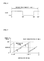
- Fig. 4 is a diagram showing the variable range of the amount of delay provided by the CMU 3.
- the CMU 3 has an ability of delaying the clock within a range of, for example, 0 to 400 degrees, as converted values corresponding to the phase of the clock. That is, as shown in Fig. 5 , in the delay characteristics of the CMU 3, if the DC voltage (i.e., manipulation voltage) of the manipulation signal varies within a range from 0 to 5 V, the phase of the clock input from the input amplifier 2 is shifted within a range from 0 to 400 degrees.
- DC voltage i.e., manipulation voltage
- the error amplifier controller 10 generates the manipulation voltage (as the manipulation signal for controlling the CMU 3 having the above-mentioned delay characteristics), which varies in a sawtooth waveform, by using the DC signal input from the error amplifier 9.
- the error amplifier controller 10 defines a lower limit LIM1 and an upper limit LIM2 on the delay characteristics of the CMU 3, and generates the manipulation voltage (i.e., manipulation signal) in a manner such that (i) when the manipulation voltage corresponding to the DC signal input from the error amplifier 9 falls below the lower limit LIM1, the error amplifier controller 10 shifts the manipulation voltage to the upper limit LIM2, and (ii) when the manipulation voltage corresponding to the DC signal input from the error amplifier 9 exceeds the upper limit LIM2, the error amplifier controller 10 shifts the manipulation voltage to the lower limit LIM1.
- manipulation voltage i.e., manipulation signal
- the amount of delay of the clock is determined by the above manipulation signal. Therefore, even if the rising point t of the clock is positioned at a phase-lead point (see Pa in Fig. 5 ) or a phase-lag point (see Pb in Fig. 5 ) with respect to the midpoint within the temporal width 2T of the input serial data, the amount of delay provided by the CMU 3 is controlled (see the arrows in Fig. 5 ) so that the rising point t of the clock is positioned at the midpoint of the temporal width 2T.
- the high-speed logic circuit is the DEMUX 5 in the above embodiment, it is not limited thereto. That is, the high-speed logic circuit may be (i) a multiplexer for converting parallel data, which belongs to a 40 GHz band, to serial data by using a clock belonging to a 40 GHz band, or (ii) a D flip-flop for latching a digital signal (of any type), which belongs to a 40 GHz band, by using a clock belonging to a 40 GHz band, and outputting the latched signal.
- Fig. 1 all structural elements shown in Fig. 1 are installed in the metal package.
- the error amplifier 9 and the error amplifier controller 10 are circuits which handle not a high-frequency signal belonging to a "GHz" band, but direct voltage. Therefore, they may be installed in a package other than the above metal package.
Landscapes
- Engineering & Computer Science (AREA)
- Computer Networks & Wireless Communication (AREA)
- Signal Processing (AREA)
- Synchronisation In Digital Transmission Systems (AREA)
- Stabilization Of Oscillater, Synchronisation, Frequency Synthesizers (AREA)
Applications Claiming Priority (1)
| Application Number | Priority Date | Filing Date | Title |
|---|---|---|---|
| JP2007261166A JP2009094638A (ja) | 2007-10-04 | 2007-10-04 | 高周波モジュール |
Publications (1)
| Publication Number | Publication Date |
|---|---|
| EP2045954A2 true EP2045954A2 (de) | 2009-04-08 |
Family
ID=39767173
Family Applications (1)
| Application Number | Title | Priority Date | Filing Date |
|---|---|---|---|
| EP08015950A Withdrawn EP2045954A2 (de) | 2007-10-04 | 2008-09-10 | Hochfrequenzmodul zur Ausführung effektiver Phasenkompensation des Taktes für ein digitales Eingangssignal |
Country Status (3)
| Country | Link |
|---|---|
| US (1) | US20090091480A1 (de) |
| EP (1) | EP2045954A2 (de) |
| JP (1) | JP2009094638A (de) |
Citations (2)
| Publication number | Priority date | Publication date | Assignee | Title |
|---|---|---|---|---|
| JP2007158415A (ja) | 2005-11-30 | 2007-06-21 | Fujitsu Ltd | 光送信装置 |
| JP2007261166A (ja) | 2006-03-29 | 2007-10-11 | Oki Electric Ind Co Ltd | 印刷確認シート作成装置,印刷確認シート,印刷確認シートの作成方法,コンピュータプログラムおよび2次元コード作成装置 |
Family Cites Families (4)
| Publication number | Priority date | Publication date | Assignee | Title |
|---|---|---|---|---|
| JP3077661B2 (ja) * | 1998-03-12 | 2000-08-14 | 日本電気株式会社 | オーバーサンプリング型クロックリカバリ回路 |
| US6292116B1 (en) * | 1999-05-17 | 2001-09-18 | Altera Corporation | Techniques and circuitry for accurately sampling high frequency data signals input to an integrated circuit |
| DE60231266D1 (de) * | 2001-03-07 | 2009-04-09 | Nippon Telegraph & Telephone | Schaltung zur Daten-und Taktrückgewinnung |
| US7139348B1 (en) * | 2002-04-09 | 2006-11-21 | Applied Micro Circuits Corporation | Distributed clock network using all-digital master-slave delay lock loops |
-
2007
- 2007-10-04 JP JP2007261166A patent/JP2009094638A/ja active Pending
-
2008
- 2008-09-09 US US12/207,053 patent/US20090091480A1/en not_active Abandoned
- 2008-09-10 EP EP08015950A patent/EP2045954A2/de not_active Withdrawn
Patent Citations (2)
| Publication number | Priority date | Publication date | Assignee | Title |
|---|---|---|---|---|
| JP2007158415A (ja) | 2005-11-30 | 2007-06-21 | Fujitsu Ltd | 光送信装置 |
| JP2007261166A (ja) | 2006-03-29 | 2007-10-11 | Oki Electric Ind Co Ltd | 印刷確認シート作成装置,印刷確認シート,印刷確認シートの作成方法,コンピュータプログラムおよび2次元コード作成装置 |
Non-Patent Citations (1)
| Title |
|---|
| CHARLES R. HOGGE, JR: "A Self Correcting Clock Recovery Circuit", IEEE JOURNAL OF LIGHTWAVE TECHNOLOGY, vol. LT-3, no. 6, December 1985 (1985-12-01), pages 1312 - 1314 |
Also Published As
| Publication number | Publication date |
|---|---|
| US20090091480A1 (en) | 2009-04-09 |
| JP2009094638A (ja) | 2009-04-30 |
Similar Documents
| Publication | Publication Date | Title |
|---|---|---|
| CN107024855B (zh) | 用于校准数字到时间转换器(dtc)的系统和方法 | |
| US8259888B2 (en) | Method of processing signal data with corrected clock phase offset | |
| JP5235190B2 (ja) | クロックデータリカバリ回路、方法ならびにそれらを利用した試験装置 | |
| JP6594710B2 (ja) | クロックデータリカバリ回路 | |
| US8781054B2 (en) | Semiconductor device | |
| KR100884170B1 (ko) | 위상동기루프용 디지털 위상 검출기 | |
| KR100367111B1 (ko) | 자기 보상 위상 검출기 | |
| CN102694760A (zh) | 调谐数字补偿滤波器的方法和数字补偿滤波器 | |
| US20050062505A1 (en) | Clock generating circuit | |
| US7139347B2 (en) | Parallel signal automatic phase adjusting circuit | |
| EP1988634B1 (de) | Pll-schaltung | |
| CN112671402B (zh) | 一种基于级联式sogi的改进型单相锁相环算法 | |
| US8971468B1 (en) | Increasing the resolution of serial data recovery units (DRUs) based on interleaved free running oversamplers | |
| CN101498761A (zh) | 锁相环系统的阶跃响应性能的测试方法 | |
| US20050141636A1 (en) | Modulator and semiconductor integrated circuit including modulator and wired or wireless communication device including modulator and semiconductor device | |
| JP4971861B2 (ja) | クロックアンドデータリカバリ回路 | |
| CN112350726A (zh) | 基于二阶跟踪环的插值系统及方法 | |
| US20090091480A1 (en) | High-frequency module for performing effective phase compensation of clock for input digital signal | |
| CN117767948B (zh) | 相位插值器非线性响应校正方法 | |
| US7453323B2 (en) | Circuit, control system, IC, transmitting and receiving apparatus, control method and program | |
| US8917129B1 (en) | Generating signals with accurate quarter-cycle intervals using digital delay locked loop | |
| JP2009014363A (ja) | 半導体試験装置 | |
| US20060203947A1 (en) | Method and apparatus for detecting linear phase error | |
| US10305499B2 (en) | Frequency synthesizer | |
| EP1271838B1 (de) | Verfahren und Vorrichtungen zum Verbessern der Jitter-Übertragung in optischen Modulen |
Legal Events
| Date | Code | Title | Description |
|---|---|---|---|
| PUAI | Public reference made under article 153(3) epc to a published international application that has entered the european phase |
Free format text: ORIGINAL CODE: 0009012 |
|
| AK | Designated contracting states |
Kind code of ref document: A2 Designated state(s): AT BE BG CH CY CZ DE DK EE ES FI FR GB GR HR HU IE IS IT LI LT LU LV MC MT NL NO PL PT RO SE SI SK TR |
|
| AX | Request for extension of the european patent |
Extension state: AL BA MK RS |
|
| RIN1 | Information on inventor provided before grant (corrected) |
Inventor name: KODAKA, HIROTOSHIC/O YOGOGAWA ELECTRIC CORPORATION Inventor name: SHIRAZAWA, FUTOSHIC/O YOGOGAWA ELECTRIC CORPORATIO Inventor name: OHASHI, MASAMICHIC/O YOGOGAWA ELECTRIC CORPORATION Inventor name: OHTA, ATSUNOBUC/O YOGOGAWA ELECTRIC CORPORATION Inventor name: KYAKUNO, TOSHIHIKOC/O YOGOGAWA ELECTRIC CORPORATIO |
|
| STAA | Information on the status of an ep patent application or granted ep patent |
Free format text: STATUS: THE APPLICATION IS DEEMED TO BE WITHDRAWN |
|
| 18D | Application deemed to be withdrawn |
Effective date: 20110401 |