EP2045643A1 - Assembly for examining microscopic preparations with a scanning microscope and lighting device for same - Google Patents
Assembly for examining microscopic preparations with a scanning microscope and lighting device for same Download PDFInfo
- Publication number
- EP2045643A1 EP2045643A1 EP08163497A EP08163497A EP2045643A1 EP 2045643 A1 EP2045643 A1 EP 2045643A1 EP 08163497 A EP08163497 A EP 08163497A EP 08163497 A EP08163497 A EP 08163497A EP 2045643 A1 EP2045643 A1 EP 2045643A1
- Authority
- EP
- European Patent Office
- Prior art keywords
- laser
- light
- optical fiber
- optical
- scanning microscope
- Prior art date
- Legal status (The legal status is an assumption and is not a legal conclusion. Google has not performed a legal analysis and makes no representation as to the accuracy of the status listed.)
- Granted
Links
- 238000002360 preparation method Methods 0.000 title 1
- 230000003287 optical effect Effects 0.000 claims abstract description 44
- 239000013307 optical fiber Substances 0.000 claims abstract description 30
- 238000005286 illumination Methods 0.000 claims abstract description 22
- 239000000463 material Substances 0.000 claims abstract description 14
- 230000006641 stabilisation Effects 0.000 claims description 7
- 238000011105 stabilization Methods 0.000 claims description 7
- 238000005562 fading Methods 0.000 claims 1
- 239000000835 fiber Substances 0.000 abstract description 26
- 230000003595 spectral effect Effects 0.000 abstract description 8
- 239000011521 glass Substances 0.000 description 6
- 238000001514 detection method Methods 0.000 description 4
- 238000001228 spectrum Methods 0.000 description 4
- 241000264877 Hippospongia communis Species 0.000 description 3
- 239000013078 crystal Substances 0.000 description 3
- 230000005284 excitation Effects 0.000 description 2
- 239000003365 glass fiber Substances 0.000 description 2
- 238000005086 pumping Methods 0.000 description 2
- 230000003716 rejuvenation Effects 0.000 description 2
- 241001631457 Cannula Species 0.000 description 1
- 238000004624 confocal microscopy Methods 0.000 description 1
- 239000003989 dielectric material Substances 0.000 description 1
- 238000000295 emission spectrum Methods 0.000 description 1
- 238000001914 filtration Methods 0.000 description 1
- 238000012423 maintenance Methods 0.000 description 1
- 230000000873 masking effect Effects 0.000 description 1
- 238000005259 measurement Methods 0.000 description 1
- 238000000034 method Methods 0.000 description 1
- 238000000386 microscopy Methods 0.000 description 1
- 238000012986 modification Methods 0.000 description 1
- 230000004048 modification Effects 0.000 description 1
- 238000004621 scanning probe microscopy Methods 0.000 description 1
- 239000004065 semiconductor Substances 0.000 description 1
- 230000001629 suppression Effects 0.000 description 1
- 239000012780 transparent material Substances 0.000 description 1
Images


Classifications
-
- G—PHYSICS
- G02—OPTICS
- G02B—OPTICAL ELEMENTS, SYSTEMS OR APPARATUS
- G02B6/00—Light guides; Structural details of arrangements comprising light guides and other optical elements, e.g. couplings
- G02B6/02—Optical fibres with cladding with or without a coating
- G02B6/02295—Microstructured optical fibre
- G02B6/02314—Plurality of longitudinal structures extending along optical fibre axis, e.g. holes
- G02B6/02342—Plurality of longitudinal structures extending along optical fibre axis, e.g. holes characterised by cladding features, i.e. light confining region
- G02B6/02376—Longitudinal variation along fibre axis direction, e.g. tapered holes
-
- G—PHYSICS
- G01—MEASURING; TESTING
- G01J—MEASUREMENT OF INTENSITY, VELOCITY, SPECTRAL CONTENT, POLARISATION, PHASE OR PULSE CHARACTERISTICS OF INFRARED, VISIBLE OR ULTRAVIOLET LIGHT; COLORIMETRY; RADIATION PYROMETRY
- G01J3/00—Spectrometry; Spectrophotometry; Monochromators; Measuring colours
- G01J3/02—Details
- G01J3/0205—Optical elements not provided otherwise, e.g. optical manifolds, diffusers, windows
- G01J3/0218—Optical elements not provided otherwise, e.g. optical manifolds, diffusers, windows using optical fibers
-
- G—PHYSICS
- G01—MEASURING; TESTING
- G01J—MEASUREMENT OF INTENSITY, VELOCITY, SPECTRAL CONTENT, POLARISATION, PHASE OR PULSE CHARACTERISTICS OF INFRARED, VISIBLE OR ULTRAVIOLET LIGHT; COLORIMETRY; RADIATION PYROMETRY
- G01J3/00—Spectrometry; Spectrophotometry; Monochromators; Measuring colours
- G01J3/02—Details
- G01J3/10—Arrangements of light sources specially adapted for spectrometry or colorimetry
-
- G—PHYSICS
- G01—MEASURING; TESTING
- G01J—MEASUREMENT OF INTENSITY, VELOCITY, SPECTRAL CONTENT, POLARISATION, PHASE OR PULSE CHARACTERISTICS OF INFRARED, VISIBLE OR ULTRAVIOLET LIGHT; COLORIMETRY; RADIATION PYROMETRY
- G01J3/00—Spectrometry; Spectrophotometry; Monochromators; Measuring colours
- G01J3/12—Generating the spectrum; Monochromators
- G01J3/1256—Generating the spectrum; Monochromators using acousto-optic tunable filter
-
- G—PHYSICS
- G02—OPTICS
- G02B—OPTICAL ELEMENTS, SYSTEMS OR APPARATUS
- G02B21/00—Microscopes
- G02B21/0004—Microscopes specially adapted for specific applications
- G02B21/002—Scanning microscopes
-
- G—PHYSICS
- G02—OPTICS
- G02B—OPTICAL ELEMENTS, SYSTEMS OR APPARATUS
- G02B21/00—Microscopes
- G02B21/0004—Microscopes specially adapted for specific applications
- G02B21/002—Scanning microscopes
- G02B21/0024—Confocal scanning microscopes (CSOMs) or confocal "macroscopes"; Accessories which are not restricted to use with CSOMs, e.g. sample holders
- G02B21/0032—Optical details of illumination, e.g. light-sources, pinholes, beam splitters, slits, fibers
-
- G—PHYSICS
- G02—OPTICS
- G02B—OPTICAL ELEMENTS, SYSTEMS OR APPARATUS
- G02B21/00—Microscopes
- G02B21/0004—Microscopes specially adapted for specific applications
- G02B21/002—Scanning microscopes
- G02B21/0024—Confocal scanning microscopes (CSOMs) or confocal "macroscopes"; Accessories which are not restricted to use with CSOMs, e.g. sample holders
- G02B21/0052—Optical details of the image generation
- G02B21/0056—Optical details of the image generation based on optical coherence, e.g. phase-contrast arrangements, interference arrangements
-
- G—PHYSICS
- G02—OPTICS
- G02B—OPTICAL ELEMENTS, SYSTEMS OR APPARATUS
- G02B21/00—Microscopes
- G02B21/0004—Microscopes specially adapted for specific applications
- G02B21/002—Scanning microscopes
- G02B21/0024—Confocal scanning microscopes (CSOMs) or confocal "macroscopes"; Accessories which are not restricted to use with CSOMs, e.g. sample holders
- G02B21/0052—Optical details of the image generation
- G02B21/0064—Optical details of the image generation multi-spectral or wavelength-selective arrangements, e.g. wavelength fan-out, chromatic profiling
-
- G—PHYSICS
- G02—OPTICS
- G02B—OPTICAL ELEMENTS, SYSTEMS OR APPARATUS
- G02B21/00—Microscopes
- G02B21/0004—Microscopes specially adapted for specific applications
- G02B21/002—Scanning microscopes
- G02B21/0024—Confocal scanning microscopes (CSOMs) or confocal "macroscopes"; Accessories which are not restricted to use with CSOMs, e.g. sample holders
- G02B21/0052—Optical details of the image generation
- G02B21/0076—Optical details of the image generation arrangements using fluorescence or luminescence
-
- G—PHYSICS
- G02—OPTICS
- G02B—OPTICAL ELEMENTS, SYSTEMS OR APPARATUS
- G02B21/00—Microscopes
- G02B21/0004—Microscopes specially adapted for specific applications
- G02B21/002—Scanning microscopes
- G02B21/0024—Confocal scanning microscopes (CSOMs) or confocal "macroscopes"; Accessories which are not restricted to use with CSOMs, e.g. sample holders
- G02B21/008—Details of detection or image processing, including general computer control
-
- G—PHYSICS
- G02—OPTICS
- G02B—OPTICAL ELEMENTS, SYSTEMS OR APPARATUS
- G02B21/00—Microscopes
- G02B21/06—Means for illuminating specimens
-
- G—PHYSICS
- G02—OPTICS
- G02B—OPTICAL ELEMENTS, SYSTEMS OR APPARATUS
- G02B6/00—Light guides; Structural details of arrangements comprising light guides and other optical elements, e.g. couplings
- G02B6/24—Coupling light guides
- G02B6/255—Splicing of light guides, e.g. by fusion or bonding
- G02B6/2552—Splicing of light guides, e.g. by fusion or bonding reshaping or reforming of light guides for coupling using thermal heating, e.g. tapering, forming of a lens on light guide ends
-
- G—PHYSICS
- G02—OPTICS
- G02F—OPTICAL DEVICES OR ARRANGEMENTS FOR THE CONTROL OF LIGHT BY MODIFICATION OF THE OPTICAL PROPERTIES OF THE MEDIA OF THE ELEMENTS INVOLVED THEREIN; NON-LINEAR OPTICS; FREQUENCY-CHANGING OF LIGHT; OPTICAL LOGIC ELEMENTS; OPTICAL ANALOGUE/DIGITAL CONVERTERS
- G02F1/00—Devices or arrangements for the control of the intensity, colour, phase, polarisation or direction of light arriving from an independent light source, e.g. switching, gating or modulating; Non-linear optics
- G02F1/35—Non-linear optics
- G02F1/353—Frequency conversion, i.e. wherein a light beam is generated with frequency components different from those of the incident light beams
-
- B—PERFORMING OPERATIONS; TRANSPORTING
- B82—NANOTECHNOLOGY
- B82Y—SPECIFIC USES OR APPLICATIONS OF NANOSTRUCTURES; MEASUREMENT OR ANALYSIS OF NANOSTRUCTURES; MANUFACTURE OR TREATMENT OF NANOSTRUCTURES
- B82Y20/00—Nanooptics, e.g. quantum optics or photonic crystals
-
- G—PHYSICS
- G02—OPTICS
- G02B—OPTICAL ELEMENTS, SYSTEMS OR APPARATUS
- G02B6/00—Light guides; Structural details of arrangements comprising light guides and other optical elements, e.g. couplings
- G02B6/02—Optical fibres with cladding with or without a coating
- G02B6/02295—Microstructured optical fibre
- G02B6/02314—Plurality of longitudinal structures extending along optical fibre axis, e.g. holes
- G02B6/02342—Plurality of longitudinal structures extending along optical fibre axis, e.g. holes characterised by cladding features, i.e. light confining region
- G02B6/02366—Single ring of structures, e.g. "air clad"
-
- G—PHYSICS
- G02—OPTICS
- G02B—OPTICAL ELEMENTS, SYSTEMS OR APPARATUS
- G02B6/00—Light guides; Structural details of arrangements comprising light guides and other optical elements, e.g. couplings
- G02B6/02—Optical fibres with cladding with or without a coating
- G02B6/02295—Microstructured optical fibre
- G02B6/02314—Plurality of longitudinal structures extending along optical fibre axis, e.g. holes
- G02B6/02342—Plurality of longitudinal structures extending along optical fibre axis, e.g. holes characterised by cladding features, i.e. light confining region
- G02B6/02371—Cross section of longitudinal structures is non-circular
-
- G—PHYSICS
- G02—OPTICS
- G02F—OPTICAL DEVICES OR ARRANGEMENTS FOR THE CONTROL OF LIGHT BY MODIFICATION OF THE OPTICAL PROPERTIES OF THE MEDIA OF THE ELEMENTS INVOLVED THEREIN; NON-LINEAR OPTICS; FREQUENCY-CHANGING OF LIGHT; OPTICAL LOGIC ELEMENTS; OPTICAL ANALOGUE/DIGITAL CONVERTERS
- G02F1/00—Devices or arrangements for the control of the intensity, colour, phase, polarisation or direction of light arriving from an independent light source, e.g. switching, gating or modulating; Non-linear optics
- G02F1/35—Non-linear optics
- G02F1/3528—Non-linear optics for producing a supercontinuum
-
- G—PHYSICS
- G02—OPTICS
- G02F—OPTICAL DEVICES OR ARRANGEMENTS FOR THE CONTROL OF LIGHT BY MODIFICATION OF THE OPTICAL PROPERTIES OF THE MEDIA OF THE ELEMENTS INVOLVED THEREIN; NON-LINEAR OPTICS; FREQUENCY-CHANGING OF LIGHT; OPTICAL LOGIC ELEMENTS; OPTICAL ANALOGUE/DIGITAL CONVERTERS
- G02F2202/00—Materials and properties
- G02F2202/32—Photonic crystals
-
- H—ELECTRICITY
- H01—ELECTRIC ELEMENTS
- H01S—DEVICES USING THE PROCESS OF LIGHT AMPLIFICATION BY STIMULATED EMISSION OF RADIATION [LASER] TO AMPLIFY OR GENERATE LIGHT; DEVICES USING STIMULATED EMISSION OF ELECTROMAGNETIC RADIATION IN WAVE RANGES OTHER THAN OPTICAL
- H01S3/00—Lasers, i.e. devices using stimulated emission of electromagnetic radiation in the infrared, visible or ultraviolet wave range
- H01S3/005—Optical devices external to the laser cavity, specially adapted for lasers, e.g. for homogenisation of the beam or for manipulating laser pulses, e.g. pulse shaping
-
- H—ELECTRICITY
- H01—ELECTRIC ELEMENTS
- H01S—DEVICES USING THE PROCESS OF LIGHT AMPLIFICATION BY STIMULATED EMISSION OF RADIATION [LASER] TO AMPLIFY OR GENERATE LIGHT; DEVICES USING STIMULATED EMISSION OF ELECTROMAGNETIC RADIATION IN WAVE RANGES OTHER THAN OPTICAL
- H01S3/00—Lasers, i.e. devices using stimulated emission of electromagnetic radiation in the infrared, visible or ultraviolet wave range
- H01S3/14—Lasers, i.e. devices using stimulated emission of electromagnetic radiation in the infrared, visible or ultraviolet wave range characterised by the material used as the active medium
- H01S3/16—Solid materials
- H01S3/1601—Solid materials characterised by an active (lasing) ion
- H01S3/162—Solid materials characterised by an active (lasing) ion transition metal
- H01S3/1625—Solid materials characterised by an active (lasing) ion transition metal titanium
-
- H—ELECTRICITY
- H01—ELECTRIC ELEMENTS
- H01S—DEVICES USING THE PROCESS OF LIGHT AMPLIFICATION BY STIMULATED EMISSION OF RADIATION [LASER] TO AMPLIFY OR GENERATE LIGHT; DEVICES USING STIMULATED EMISSION OF ELECTROMAGNETIC RADIATION IN WAVE RANGES OTHER THAN OPTICAL
- H01S3/00—Lasers, i.e. devices using stimulated emission of electromagnetic radiation in the infrared, visible or ultraviolet wave range
- H01S3/14—Lasers, i.e. devices using stimulated emission of electromagnetic radiation in the infrared, visible or ultraviolet wave range characterised by the material used as the active medium
- H01S3/16—Solid materials
- H01S3/163—Solid materials characterised by a crystal matrix
- H01S3/1631—Solid materials characterised by a crystal matrix aluminate
- H01S3/1636—Al2O3 (Sapphire)
Definitions
- the invention relates to an arrangement for examining microscopic specimens with a scanning microscope.
- the invention relates to an arrangement for examining microscopic specimens with a scanning microscope comprising a laser and an optical means which images the light generated by the laser on a sample to be examined.
- the scanning microscope can also be designed as a confocal microscope.
- the invention relates to a lighting device for a scanning microscope.
- Confocal Microscope System for Multicolor Fluorescence is, for example, an arrangement with a single laser emitting a plurality of laser lines. At present, mostly mixed gas lasers, in particular ArKr lasers, are used for this purpose.
- diode lasers and solid-state lasers are used.
- the emission spectrum of lasers is limited to a narrow wavelength range, so that for simultaneous multi-line excitation, the light of several lasers must be combined into one illumination beam.
- the gas laser used most often as a multi-line laser are very complicated and expensive. In addition, they require a lot of maintenance, which makes continuous use difficult in many microscopic applications.
- the invention has for its object to provide a scanning microscope, which allows the sample examination with multiple spectral lines, without relying on the use of the multi-line laser.
- the objective object is achieved by an arrangement which is characterized in that an optical component is provided between the laser and the optical means, which widens spectrally the light generated by the laser with a single pass.
- a further object of the invention is to provide a lighting device for a scanning microscope, which makes available additional spectral ranges that were previously not addressable.
- the objective object is achieved by a lighting device, which is characterized in that at the light exit opening, an optical component is mounted, which consists of photonic band gap material.
- the optical component in the form of a "photonic band-gap material” has the advantage that a short laser pulse is widened by the optically non-linear structure of the fiber and thus a spectrally broad, continuous light spectrum is formed.
- Photonic-band-gap-material is a microstructured transparent material. Usually by combining different dielectrics, the resulting crystal can be given a band structure for photons reminiscent of the electronic band structure of semiconductors.
- the technique is now also being implemented in optical fibers.
- the fibers are made by removing structured glass tubes.
- the fibers are based on a special structure: In the fiber direction small needles are left free, which have a distance of about 2-3 microns and a diameter of about 1 micron and are usually filled with air. There is no cannula in the middle of the fiber.
- These types of fibers are known as "photon crystal fibers", “holey fibers” or "microstructured fibers”.
- Photon crystal fibers can be used to create a continuous spectral distribution over the entire visible wavelength range.
- the light of a short pulse laser is coupled into the fiber. Due to the optically non-linear structure of the fiber, the frequency spectrum of the laser widens. The result is a spectrally broad, continuous light spectrum.
- the optical component is constructed in a preferred embodiment of the scanning microscope of a plurality of micro-optical structural elements having at least two different optical densities.
- the optical element includes a first region and a second region, wherein the first region has a homogeneous structure and in the second region a microscopic structure of microoptical structural elements is formed. It is also advantageous if the first area encloses the second area.
- the micro-optical structural elements are preferably cannulas, webs, honeycombs, tubes or cavities.
- the optical component consists in another embodiment of juxtaposed glass or plastic material and cavities. Particularly preferred is the embodiment in which the optical component consists of photonic band gap material and designed as an optical fiber, wherein preferably an optical diode is provided which suppresses a back reflection of the light beam of the laser at the ends of the optical fiber
- a particularly preferred embodiment variant that is easy to implement includes as optical component a conventional optical fiber with a fiber core, which has a taper at least along a section.
- Optical fibers of this type are known as so-called "tapered fibers".
- the optical fiber is a total of 1 m long and has a taper to a length of 30 mm to 90 mm.
- the diameter of the fiber is in a preferred embodiment 150 microns outside the region of the taper and that of the fiber core in this area about 8 microns. In the area of rejuvenation is the diameter of the fiber reduced to approx. 2 ⁇ m.
- the fiber core diameter is correspondingly in the nanometer range.
- such a fiber laser can advantageously be combined with acousto-optical or electro-optical, adjustable filters (AOTF), with acousto-electro-optical deflectors (AOD), acousto-optical or electro-optical beam splitters (AOBS).
- AOTF adjustable filters
- AOD acousto-electro-optical deflectors
- AOBS electro-optical beam splitters
- the fiber exit end can be used as a point light source, making the use of an excitation diaphragm superfluous.
- devices for compensation of light power fluctuations are provided.
- a control loop for light power stabilization can be installed, which parasitically measures the light output in the beam path of the microscope and, for example, by varying the pumping light power or with the help of an acousto-or electro-optical element, the sample illumination light power keeps constant.
- LCD attenuators could also be used for this purpose.
- a further advantage of the invention is that, if the lighting device is already designed accordingly, it supplies a plurality of spectral regions for illumination.
- the laser which represents the illumination device for a scanning microscope, has attached to the light exit opening an optical component.
- the optical component consists of photonic band gap material.
- the photonic band gap material can be designed as an optical fiber.
- Fig. 1 shows a confocal microscope, which uses an optical device 3 for expanding a laser pulse generated by a pulse laser 1.
- the pulse laser 1 defines a pulsed laser beam 2, which is passed through the optical component 3.
- the optical component 3 is a "photonic band gap material.”
- a spectrally broadband illumination light 4 emerges from the optical component 3 and is imaged by a first optic 5 onto an illumination pinhole 6 and then impinges on a beam splitter 7. From the beam splitter 7, the spectrally broadband illumination light 4 passes to a second optical system 8, which generates a parallel light beam 4a which strikes a scanning mirror 9.
- the scanning mirror 9 is followed by a plurality of optics 10 and 11, which form the light beam 4a Lens 12 from which it is imaged onto a sample 13.
- the light reflected or emitted by the sample defines an observation beam path 4b.
- the light from the observation beam path 4b again passes through the second optics 8 and is imaged onto a detection pinhole 14 in front of a detector
- the optical component 3 it is possible that necessary for the examination of the sample 13 ige laser light according to the desired spectrum to produce.
- Fig. 2 illustrated embodiment shows a confocal microscope, was waived in the illumination pinhole 6. All elements made with the elements Fig. 1 are identical, are denoted by the same reference numeral.
- an AOTF 16 acousto-optical tunable filter
- the optical Component 3 can produce a broadband illumination light 4, it is necessary to provide means for wavelength selection and light power stabilization. It is advantageously possible to combine acousto-optically or electro-optically adjustable filters (AOTF) with acousto-optical or electro-optical deflectors (AOD) and acousto-optical or electro-optical beam splitters (AOBS). These can be used for wavelength selection as well as for masking the detection light.
- the AOTF 16 is also associated with a beam sump 18, which captures the unused spectral components of the illumination light to avoid unnecessary interference of the scanning microscope.
- FIG. 3 Another embodiment of the invention is in Fig. 3 shown.
- an optical fiber 20 is used which consists of the photonic band gap material.
- the pulsed laser beam 2 is coupled via an optical system 19 into an input end 20a of the optical fiber 20.
- the optical fiber 20 is composed of the photonic band-gap material, emerges from an outlet end 20b, a spectrally broadened laser pulse, which is coupled out via an optical system 21.
- a spectral filtering is performed before the spectrally broadened laser pulse impinges on the illumination pinhole 6, a spectral filtering is performed.
- a plurality of color filters 24 are arranged on a revolver 23.
- a motor 22 rotates the turret 23 so that the corresponding color filters 24 can be introduced into the beam path.
- a linear arrangement of the color filter 24 is conceivable, while the color filter 24 are moved by means of a linear movement in an illumination beam path 50.
- the illumination beam path 50 after the illumination pinhole 6 is aligned with the beam path Fig. 1 comparable.
- the beam splitter 7 directs the light onto the scanning mirror 9. Part of the light passes through the beam splitter 7 and defines a lost beam path 50a. This portion of the light is lost for observation or measurement.
- a detector 25 is provided in the loss beam path 50a, which determines the loss of light and determines therefrom an electronic variable, which is passed by means of a line 30 to a control electronics 26.
- the control electronics 26 is connected via a further line 32 to the pulse laser. 1 connected. Via the line 32, the control electronics 26 regulates the intensity of the pulse laser 1 in such a way that always a constant light output impinges on the sample 13.
- a control loop for light power stabilization may be provided such that it parasitically measures the light power in the beam path of the microscope and, for example, by varying the pumping light power or with the aid of an acousto-or electro-optical element, the sample illumination light power keeps constant.
- LCD attenuators could also be used for this purpose.
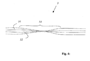
- Fig. 4 schematically shows an embodiment of the optical component 3.
- the optical component 3 consists of a conventional optical fiber 51 having an outer diameter of 125 microns and a fiber core 52 having a diameter of 6 microns.
- the outer diameter of the optical fiber 51 is reduced to 1.8 ⁇ m.
- the diameter of the fiber core 52 is only fractions of micrometers.
- Fig. 5 shows an embodiment of the optical device 3.
- This consists of photonic band gap material having a particular honeycomb microstructure 54.
- the honeycomb structure shown is particularly suitable for the generation of broadband light.
- the diameter of the inner cannula 55 is about 1.9 microns.
- the inner cannula 55 is surrounded by glass webs 56.
- the glass webs 56 form honeycomb-shaped cavities 57.
- These micro-optical structural elements together form a second region 58, which is surrounded by a first region 59, the glass jacket is executed.
Abstract
Description
Die Erfindung betrifft eine Anordnung zum Untersuchen mikroskopischer Präparate mit einem Scanmikroskop. Im Besonderen betrifft die Erfindung eine Anordnung zum Untersuchen mikroskopischer Präparate mit einem Scanmikroskop, das einen Laser und ein optisches Mittel umfasst, das das von dem Laser erzeugte Licht auf eine zu untersuchende Probe abbildet. Das Scanmikroskop kann auch als konfokales Mikroskop ausgestaltet sein.The invention relates to an arrangement for examining microscopic specimens with a scanning microscope. In particular, the invention relates to an arrangement for examining microscopic specimens with a scanning microscope comprising a laser and an optical means which images the light generated by the laser on a sample to be examined. The scanning microscope can also be designed as a confocal microscope.
Des Weiteren betrifft die Erfindung eine Beleuchtungseinrichtung für ein Scanmikroskop.Furthermore, the invention relates to a lighting device for a scanning microscope.
In der Scanmikroskopie wird eine Probe mit einem Lichtstrahl abgerastert. Hierzu werden oft Laser als Lichtquelle eingesetzt. Aus der
Im Einsatz sind auch Diodenlaser und Festkörperlaser.Also in use are diode lasers and solid-state lasers.
Aus der Patenschrift
Das Emissionsspektrum von Lasern ist auf einen schmalen Wellenlängenbereich eingegrenzt, so dass zur simultanen Mehrlinienanregung das Licht mehrerer Laser zu einem Beleuchtungsstrahl vereinigt werden muss.The emission spectrum of lasers is limited to a narrow wavelength range, so that for simultaneous multi-line excitation, the light of several lasers must be combined into one illumination beam.
Die als Mehrlinienlaser meist eingesetzten Gaslaser sind sehr aufwendig und teuer. Darüber hinaus sind sie sehr wartungsbedürftig, was den Dauereinsatz bei vielen mikroskopischen Anwendungen erschwert.The gas laser used most often as a multi-line laser are very complicated and expensive. In addition, they require a lot of maintenance, which makes continuous use difficult in many microscopic applications.
Der Erfindung liegt die Aufgabe zugrunde, ein Scanmikroskop zu schaffen, das die Probenuntersuchung mit mehreren spektralen Linien ermöglicht, ohne dabei auf den Einsatz vom Mehrlinienlaser angewiesen zu sein.The invention has for its object to provide a scanning microscope, which allows the sample examination with multiple spectral lines, without relying on the use of the multi-line laser.
Die objektive Aufgabe wird gelöst durch eine Anordnung, die dadurch gekennzeichnet ist, dass zwischen dem Laser und dem optischen Mittel ein optisches Bauelement vorgesehen ist, das das vom Laser erzeugte Licht bei einmaligem Durchlauf spektral verbreitert.The objective object is achieved by an arrangement which is characterized in that an optical component is provided between the laser and the optical means, which widens spectrally the light generated by the laser with a single pass.
Eine weitere Aufgabe der Erfindung ist es, eine Beleuchtungseinrichtung für ein Scanmikroskop zu schaffen, die weitere spektrale Bereiche zugänglich macht, die bisher nicht adressierbar waren.A further object of the invention is to provide a lighting device for a scanning microscope, which makes available additional spectral ranges that were previously not addressable.
Die objektive Aufgabe wird gelöst durch eine Beleuchtungseinrichtung, die dadurch gekennzeichnet ist, dass an der Lichtaustrittsöffnung ein optisches Bauelement angebracht ist, das aus photonic-band-gap-material besteht.The objective object is achieved by a lighting device, which is characterized in that at the light exit opening, an optical component is mounted, which consists of photonic band gap material.
Das optische Bauelement in der Form eines "photonic-band-gap-material" hat den Vorteil, dass durch den optisch nichtlinearen Aufbau der Faser ein kurzer Laserimpuls verbreitert wird und somit ein spektral breites, kontinuierliches Lichtspektrum entsteht. Bei "Photonic-band-gap-material" handelt es sich um mikrostrukturiertes durchsichtiges Material. Meist durch Zusammenfügen von verschiedenen Dielektrika lässt sich dem resultierenden Kristall eine Bandstruktur für Photonen aufprägen, die an die elektronische Bandstruktur von Halbleitern erinnert.The optical component in the form of a "photonic band-gap material" has the advantage that a short laser pulse is widened by the optically non-linear structure of the fiber and thus a spectrally broad, continuous light spectrum is formed. "Photonic-band-gap-material" is a microstructured transparent material. Mostly by combining different dielectrics, the resulting crystal can be given a band structure for photons reminiscent of the electronic band structure of semiconductors.
Die Technik wird neuerdings auch bei Lichtleitfasern verwirklicht. Die Fasern werden durch Ausziehen von strukturiert angeordneten Glasrohren hergestellt. Den Fasern liegt eine besondere Struktur zugrunde: In Faserrichtung sind kleine Kanülen frei gelassen, die einen Abstand von etwa 2-3 µm und einen Durchmesser von ca. 1 µm haben und meist mit Luft gefüllt sind. In der Mitte der Faser liegt keine Kanüle vor. Diese Art von Fasern sind als "photon crystal fibres", "holey fibers" oder "microstructured fibers" bekannt.The technique is now also being implemented in optical fibers. The fibers are made by removing structured glass tubes. The fibers are based on a special structure: In the fiber direction small needles are left free, which have a distance of about 2-3 microns and a diameter of about 1 micron and are usually filled with air. There is no cannula in the middle of the fiber. These types of fibers are known as "photon crystal fibers", "holey fibers" or "microstructured fibers".
"Photon crystal fibres" können für die Erzeugung einer kontinuierlichen spektralen Verteilung über den gesamten sichtbaren Wellenlängenbereich eingesetzt werden. Hierzu wird das Licht eines Kurzpulslasers in die Faser eingekoppelt. Durch den optisch nichtlinearen Aufbau der Faser verbreitert sich das Frequenzspektrum des Lasers. Es entsteht ein spektral breites, kontinuierliches Lichtspektrum."Photon crystal fibers" can be used to create a continuous spectral distribution over the entire visible wavelength range. For this purpose, the light of a short pulse laser is coupled into the fiber. Due to the optically non-linear structure of the fiber, the frequency spectrum of the laser widens. The result is a spectrally broad, continuous light spectrum.
Das optische Bauelement ist in einer bevorzugten Ausgestaltung des Scanmikroskops aus einer Vielzahl von mikrooptischen Strukturelementen aufgebaut, die zumindest zwei unterschiedliche optische Dichten aufweisen. Ganz besonders bevorzugt ist eine Ausgestaltung, bei der das optische Element einen ersten Bereich und einen zweiten Bereich beinhaltet, wobei der erste Bereich eine homogene Struktur aufweist und in dem zweiten Bereich eine mikroskopische Struktur aus mikrooptischen Strukturelementen gebildet ist. Von Vorteil ist es außerdem, wenn der erste Bereich den zweiten Bereich umschließt. Die mikrooptischen Strukturelemente sind vorzugsweise Kanülen, Stege, Waben, Röhren oder Hohlräume.The optical component is constructed in a preferred embodiment of the scanning microscope of a plurality of micro-optical structural elements having at least two different optical densities. Very particular preference is given to an embodiment in which the optical element includes a first region and a second region, wherein the first region has a homogeneous structure and in the second region a microscopic structure of microoptical structural elements is formed. It is also advantageous if the first area encloses the second area. The micro-optical structural elements are preferably cannulas, webs, honeycombs, tubes or cavities.
Das optische Bauelement besteht in einer anderen Ausgestaltung aus nebeneinander angeordnetem Glas- oder Kunststoffmaterial und Hohlräumen. Besonders zu bevorzugen ist die Ausführungsvariante, bei der das optische Bauelement aus Photonic-Band-Gap-Material besteht und als Lichtleitfaser ausgestaltet, wobei vorzugsweise eine optische Diode vorgesehen ist, die eine Rückreflexion des Lichtstrahles unterdrückt des Lasers an den Enden der LichtleitfaserThe optical component consists in another embodiment of juxtaposed glass or plastic material and cavities. Particularly preferred is the embodiment in which the optical component consists of photonic band gap material and designed as an optical fiber, wherein preferably an optical diode is provided which suppresses a back reflection of the light beam of the laser at the ends of the optical fiber
Eine ganz besonders bevorzugte und einfach zu realisierende Ausführungsvariante beinhaltet als optisches Bauelement eine herkömmliche Lichtleitfaser mit einem Faserkern, die zumindest entlang eines Teilstücks eine Verjüngung aufweist. Lichtleitfasern dieser Art sind als sog. "tapered fibers" bekannt. Vorzugsweise ist die Lichtleitfaser insgesamt 1 m lang und weist eine Verjüngung auf einer Länge von 30 mm bis 90 mm auf. Der Durchmesser der Faser beträgt in einer bevorzugten Ausgestaltung 150 µm außerhalb des Bereich der Verjüngung und der des Faserkerns in diesem Bereich ca. 8 µm. Im Bereich der Verjüngung ist der Durchmesser der Faser auf ca. 2 µm reduziert. Der Faserkern Durchmesser liegt entsprechend im Nanometerbereich.A particularly preferred embodiment variant that is easy to implement includes as optical component a conventional optical fiber with a fiber core, which has a taper at least along a section. Optical fibers of this type are known as so-called "tapered fibers". Preferably, the optical fiber is a total of 1 m long and has a taper to a length of 30 mm to 90 mm. The diameter of the fiber is in a preferred embodiment 150 microns outside the region of the taper and that of the fiber core in this area about 8 microns. In the area of rejuvenation is the diameter of the fiber reduced to approx. 2 μm. The fiber core diameter is correspondingly in the nanometer range.
Zum Einsatz in der Mikroskopie ist es wichtig, Mittel zur Wellenlängenauswahl und zur Lichtleistungsstabilisierung zu implementieren. Daher lässt sich in vorteilhafter Weise ein solcher Faserlaser mit akusto- oder elektrooptischen, einstellbaren Filtern (AOTF), mit akusto- oder elektrooptischen Deflektoren (AOD), akusto- oder elektrooptischen Strahlteilern (AOBS) kombinieren. Diese können zum einen zur Wellenlängenauswahl als auch zur Ausblendung des Detektionslichtes verwendet werden (unsere deutsche Anmeldung
Insbesondere in der konfokalen Mikroskopie läßt sich das Faseraustrittsende als Punktlichtquelle nutzen, wodurch die Verwendung einer Anregungsblende überflüssig wird. Bei einer solchen Ausgestaltung wäre es von besonderem Vorteil, das Faserende selbst teilreflektierend zu beschichten, so dass dieser Teilreflektor einen Resonatorendspiegel bildet.Particularly in confocal microscopy, the fiber exit end can be used as a point light source, making the use of an excitation diaphragm superfluous. In such an embodiment, it would be particularly advantageous to coat the fiber end itself partially reflective, so that this partial reflector forms a Resonatorendspiegel.
In weiteren Ausführungsformen sind Vorrichtungen zur Kompensation von Lichtleistungsschwankungen vorgesehen. Beispielsweise kann eine Regelschleife zur Lichtleistungsstabilisierung eingebaut werden, die parasitär die Lichtleistung im Strahlengang des Mikroskops misst und beispielsweise durch Variation der Pumplichtleistung oder mit Hilfe eines akusto- oder elektrooptischen Elements die Probenbeleuchtungslichtleistung konstant hält. Zu diesem Zweck könnten auch LCD-Abschwächer verwendet werden.In further embodiments, devices for compensation of light power fluctuations are provided. For example, a control loop for light power stabilization can be installed, which parasitically measures the light output in the beam path of the microscope and, for example, by varying the pumping light power or with the help of an acousto-or electro-optical element, the sample illumination light power keeps constant. LCD attenuators could also be used for this purpose.
Ein weiterer Vorteil der Erfindung ist, wenn die Beleuchtungeeinrichtung bereits entsprechend gestaltet ist, dass sie mehrere spektrale Bereiche zur Beleuchtung liefert. Der Laser, der die Beleuchtungseinrichtung für ein Scanmikroskop darstellt, hat an der Lichtaustrittsöffnung ein optisches Bauelement befestigt. Das optische Bauelement besteht aus photonic-band-gap-material. Ferner kann das photonic-band-gap-material als Lichtleitfaser ausgestaltet sein.A further advantage of the invention is that, if the lighting device is already designed accordingly, it supplies a plurality of spectral regions for illumination. The laser, which represents the illumination device for a scanning microscope, has attached to the light exit opening an optical component. The optical component consists of photonic band gap material. Furthermore, the photonic band gap material can be designed as an optical fiber.
In der Zeichnung ist der Erfindungsgegenstand schematisch dargestellt und wird anhand der Figuren nachfolgend beschrieben. Dabei zeigen:
- Fig. 1
- eine erfindungsgemäße Anordnung mit einem Konfokalmikroskop,
- Fig. 2
- eine Anordnung, bei der auf ein Beleuchtungspinhole verzichtet wurde,
- Fig. 3
- eine Anordnung mit Lichtleistungsstabilisierung,
- Fig. 4
- eine Ausführung des optischen Bauelements
- Fig. 5
- eine weitere Ausführung des optischen Bauelements.
- Fig. 1
- an arrangement according to the invention with a confocal microscope,
- Fig. 2
- an arrangement in which a lighting pinhole was dispensed with,
- Fig. 3
- an arrangement with light power stabilization,
- Fig. 4
- an embodiment of the optical component
- Fig. 5
- a further embodiment of the optical component.
Das in
Eine weitere Ausführungsform der Erfindung ist in
Die Erfindung wurde in Bezug auf eine besondere Ausführungsform beschrieben. Es ist jedoch selbstverständlich, dass Änderungen und Abwandlungen durchgeführt werden können, ohne dabei den Schutzbereich der nachstehenden Ansprüche zu verlassen.The invention has been described with reference to a particular embodiment. However, it is to be understood that changes and modifications may be made without departing from the scope of the following claims.
- 11
- Pulslaserpulse laser
- 22
- Gepulster LaserstrahlPulsed laser beam
- 33
- optisches Bauelementoptical component
- 44
- Spektral breitbandiges BeleuchtungslichtSpectral broadband illumination light
- 4a4a
- Lichtstrahlbeam of light
- 4b4b
- BeobachtungsstrahlengangObservation beam path
- 55
- Optikoptics
- 66
- BeleuchtungspinholeIllumination pinhole
- 77
- Strahlteilerbeamsplitter
- 88th
- Optikoptics
- 99
- Scanspiegelscanning mirror
- 1010
- Optikoptics
- 1111
- Optikoptics
- 1212
- Objektivlens
- 1313
- Probesample
- 1414
- DetektionspinholeDetection pinhole
- 1515
- Detektordetector
- 1616
- AOTF (acousto optical tunable filter)AOTF (acousto optical tunable filter)
- 1717
- AOTF-AnsteuerungAOTF control
- 1818
- Strahlsumpfray marsh
- 1919
- Optikoptics
- 2020
- photonic-band-gap-LichtleitfaserPhotonic-band-gap optical fiber
- 20a20a
- Eintrittsendeentry end
- 20b20b
- Austrittsendeexit end
- 2121
- Optikoptics
- 2222
- Motorengine
- 2323
- Revolverrevolver
- 2424
- Farbfiltercolor filter
- 2525
- Detektordetector
- 2626
- Regelungselektronikcontrol electronics
- 3030
- Leitungmanagement
- 3232
- Leitungmanagement
- 5050
- BeleuchtungsstrahlengangIllumination beam path
- 50a50a
- VerluststrahlengangLoss optical path
- 5151
- Lichtleitfaseroptical fiber
- 5252
- Faserkernfiber core
- 5353
- Verjüngungrejuvenation
- 5454
- Mikrostrukturmicrostructure
- 5555
- Kanülecannula
- 5656
- Glasstegeglass webs
- 5757
- Hohlräumecavities
- 5858
- zweiter Bereichsecond area
- 5959
- erster Bereichfirst area
Claims (8)
das einen Laser (1) und ein optisches Mittel (12) umfasst, das das von dem Laser (1) erzeugte Licht auf eine zu untersuchende Probe (13) abbildet,
wobei ein akustooptisches Filter (AOTF 16) mit einer AOTF-Ansteuerung als Mittel zur Wellenlängenauswahl (16) und eine Lichtleitfaser (3, 20, 51) vorgesehen sind,
dadurch gekennzeichnet, dass zwischen dem als Pulslaser (1) ausgebildeten Laser und dem optischen Mittel (12) ein optisches Bauelement (3, 20, 51) vorgesehen ist, das das vom Pulslaser (1) erzeugte Licht bei einmaligem Durchlauf spektral verbreitert, derart, dass aus ihm ein spektral breitbandiges Beleuchtungslicht (4) austritt,
wobei die Lichtleitfaser (3, 20, 51) das optische Bauelement bildet,
die Mittel zur Wellenlängenauswahl Mittel (16) zum Abschwächen und/oder Ausblenden des Lichts mindestens einer Wellenlänge oder mindestens eines Wellenlängenbereichs umfassen und der Lichtleitfaser (3, 20, 51) nachgeordnet sind,
dass die Lichtleitfaser aus Photonic-Band-Gap-Material besteht,
und dass eine optische Diode zwischen dem Laser und der Lichtleitfaser vorgesehen ist, die eine Rückreflexion des Lichtstrahls des Lasers, die von den Enden der Lichtleitfaser herrührt, unterdrückt.Arrangement for examining microscopic specimens with a scanning microscope,
which comprises a laser (1) and an optical means (12) which images the light generated by the laser (1) onto a sample (13) to be examined,
an acoustooptic filter (AOTF 16) having an AOTF drive as wavelength selection means (16) and an optical fiber (3, 20, 51) being provided,
characterized in that an optical component (3, 20, 51) is provided between the laser formed as a pulse laser (1) and the optical means (12), which spectrally broadens the light generated by the pulse laser (1) in a single pass, in such a way in that a spectrally broadband illumination light (4) emerges from it,
wherein the optical fiber (3, 20, 51) forms the optical component,
the means for wavelength selection comprise means (16) for attenuating and / or fading out the light of at least one wavelength or at least one wavelength range and are arranged downstream of the optical fiber (3, 20, 51),
that the optical fiber consists of photonic band gap material,
and that an optical diode is provided between the laser and the optical fiber, which suppresses back reflection of the light beam of the laser originating from the ends of the optical fiber.
mit einem Laser (1), der eine Lichtaustrittsöffnung umfasst,
wobei ein akustooptisches Filter (AOTF 16) mit einer AOTF-Ansteuerung als Mittel zur Wellenlängenauswahl (16) und eine Lichtleitfaser (3, 20, 51) vorgesehen sind,
dadurch gekennzeichnet, dass der Laser als Pulslaser (1) ausgebildet ist, dessen Licht über die Lichtaustrittsöffnung einem optischen Bauelement (3, 20, 51) zugeführt ist, das das vom Pulslaser (1) erzeugte Licht bei einmaligem Durchlauf spektral verbreitert, derart, dass aus ihm ein spektral breitbandiges Beleuchtungslicht (4) austritt,
wobei die Lichtleitfaser (3, 20, 51) das optische Bauelement bildet,
die Mittel zur Wellenlängenauswahl Mittel (16, 18; 23, 24) zum Abschwächen und/oder Ausblenden des Lichts mindestens einer Wellenlänge oder mindestens eines Wellenlängenbereichs umfassen und der Lichtleitfaser (3, 20, 51) nachgeordnet sind,
dass die Lichtleitfaser aus Photonic-Band-Gap-Material besteht,
und dass eine optische Diode zwischen dem Laser und der Lichtleitfaser vorgesehen ist, die eine Rückreflexion des Lichtstrahls des Lasers, die von den Enden der Lichtleitfaser herrührt, unterdrückt.Illumination device for a scanning microscope,
with a laser (1) comprising a light exit opening,
an acoustooptic filter (AOTF 16) having an AOTF drive as wavelength selection means (16) and an optical fiber (3, 20, 51) being provided,
characterized in that the laser is designed as a pulse laser (1) whose light is supplied via the light exit opening to an optical component (3, 20, 51) which spectrally widens the light generated by the pulsed laser (1) in a single pass such that a spectrally broadband illumination light (4) emerges from it,
wherein the optical fiber (3, 20, 51) forms the optical component,
the means for wavelength selection means (16, 18; 23, 24) for attenuating and / or hiding the light of at least one wavelength or at least one wavelength range and are arranged downstream of the optical fiber (3, 20, 51),
that the optical fiber consists of photonic band gap material,
and that an optical diode is provided between the laser and the optical fiber, which suppresses back reflection of the light beam of the laser originating from the ends of the optical fiber.
Applications Claiming Priority (3)
| Application Number | Priority Date | Filing Date | Title |
|---|---|---|---|
| DE10030013 | 2000-06-17 | ||
| DE10115509A DE10115509A1 (en) | 2000-06-17 | 2001-03-29 | Arrangement for examining microscopic specimens with a scanning microscope and illumination device for a scanning microscope |
| EP01112880A EP1164400B1 (en) | 2000-06-17 | 2001-06-01 | Device for investigating microscopic slide preparations with a scanning microscope and illuminating device for a scanning microscope |
Related Parent Applications (2)
| Application Number | Title | Priority Date | Filing Date |
|---|---|---|---|
| EP01112880.8 Division | 2001-06-01 | ||
| EP01112880A Division EP1164400B1 (en) | 2000-06-17 | 2001-06-01 | Device for investigating microscopic slide preparations with a scanning microscope and illuminating device for a scanning microscope |
Publications (3)
| Publication Number | Publication Date |
|---|---|
| EP2045643A1 true EP2045643A1 (en) | 2009-04-08 |
| EP2045643B1 EP2045643B1 (en) | 2010-04-28 |
| EP2045643B2 EP2045643B2 (en) | 2013-10-30 |
Family
ID=7646174
Family Applications (3)
| Application Number | Title | Priority Date | Filing Date |
|---|---|---|---|
| EP08163497.4A Expired - Lifetime EP2045643B2 (en) | 2000-06-17 | 2001-06-01 | Scanning microscope for examining microscopic preparations and lighting device for same |
| EP08163494A Ceased EP2045642A1 (en) | 2000-06-17 | 2001-06-09 | Scanning microscope |
| EP08163492A Ceased EP2045641A3 (en) | 2000-06-17 | 2001-06-15 | Illumination device |
Family Applications After (2)
| Application Number | Title | Priority Date | Filing Date |
|---|---|---|---|
| EP08163494A Ceased EP2045642A1 (en) | 2000-06-17 | 2001-06-09 | Scanning microscope |
| EP08163492A Ceased EP2045641A3 (en) | 2000-06-17 | 2001-06-15 | Illumination device |
Country Status (6)
| Country | Link |
|---|---|
| US (1) | US7679822B2 (en) |
| EP (3) | EP2045643B2 (en) |
| JP (1) | JP5111480B2 (en) |
| AT (1) | ATE407381T1 (en) |
| DE (13) | DE10115589B4 (en) |
| DK (1) | DK1184701T3 (en) |
Families Citing this family (26)
| Publication number | Priority date | Publication date | Assignee | Title |
|---|---|---|---|---|
| WO2003060610A1 (en) * | 2002-01-16 | 2003-07-24 | Carl Zeiss Jena Gmbh | Methods and systems for microscopic imaging |
| DE10211458A1 (en) * | 2002-03-12 | 2003-09-25 | Zeiss Carl Jena Gmbh | Laser scanning microscope has photon correlated light source and a heterodyne detection arrangement that act in conjunction to improve the resolution of a confocal microscope |
| DE10221365A1 (en) * | 2002-05-08 | 2003-11-27 | Jenoptik Laser Optik Sys Gmbh | Optical arrangement for generating a broadband spectrum |
| DE10227111B4 (en) | 2002-06-17 | 2007-09-27 | Leica Microsystems Cms Gmbh | Spectral microscope and method for data acquisition with a spectral microscope |
| DE10313987B4 (en) * | 2003-03-27 | 2007-07-12 | Leica Microsystems Cms Gmbh | Device and method for illuminating an object |
| DE10314750A1 (en) * | 2003-03-31 | 2004-11-04 | Leica Microsystems Heidelberg Gmbh | Scanning microscope for biological applications has an objective with a contrast device which enables use of the microscope in a Hoffman-modulation contrast mode |
| DE10324478B3 (en) | 2003-05-30 | 2004-12-09 | Leica Microsystems Heidelberg Gmbh | Device for determining the light output of a light beam and scanning microscope |
| DE10331906B4 (en) * | 2003-07-15 | 2005-06-16 | Leica Microsystems Heidelberg Gmbh | Light source with a microstructured optical element and microscope with light source |
| DE10340964A1 (en) | 2003-09-05 | 2005-03-31 | Leica Microsystems Heidelberg Gmbh | Light source with a microstructured optical element |
| DE102004032463B4 (en) * | 2004-06-30 | 2011-05-19 | Jenoptik Laser Gmbh | Method and optical arrangement for generating a broadband spectrum by means of mode-locked picosecond laser pulses |
| AU2005313736A1 (en) * | 2004-12-08 | 2006-06-15 | Thomas Buehrer | Optical device for producing lines of light from quasi-point sources of light by means of slit-like cavities |
| DE102005010887A1 (en) * | 2005-03-09 | 2006-09-14 | Leica Microsystems (Schweiz) Ag | lighting device |
| DE102006004075B4 (en) * | 2006-01-28 | 2008-01-03 | Leica Microsystems Cms Gmbh | An apparatus and method for reducing intensity noise and a microscope having an intensity noise reduction device |
| DE102006053187A1 (en) | 2006-11-09 | 2008-05-15 | Leica Microsystems Cms Gmbh | Acousto-optic component |
| DE102007024075B4 (en) | 2007-05-22 | 2022-06-09 | Leica Microsystems Cms Gmbh | Tunable acousto-optic filter element, adjustable light source, microscope and acousto-optic beam splitter |
| DE102007028337B4 (en) * | 2007-06-15 | 2019-08-29 | Leica Microsystems Cms Gmbh | Beam combiner and a light source with such a beam combiner |
| DE102007039498B4 (en) | 2007-08-21 | 2017-08-03 | Leica Microsystems Cms Gmbh | Method and device for illuminating and / or irradiating an object or a sample |
| DE102007053199A1 (en) | 2007-11-06 | 2009-05-14 | Leica Microsystems Cms Gmbh | Device and method for controlling an acousto-optic component |
| GB0800936D0 (en) | 2008-01-19 | 2008-02-27 | Fianium Ltd | A source of optical supercontinuum generation having a selectable pulse repetition frequency |
| DE202009007789U1 (en) | 2009-06-03 | 2009-08-20 | Carl Zeiss Microimaging Gmbh | Broadband light source and microscope |
| DE102009056092B4 (en) | 2009-11-30 | 2013-02-28 | PicoQuant GmbH. Unternehmen für optoelektronische Forschung und Entwicklung | Light source with a diode laser |
| US9229294B2 (en) | 2010-05-06 | 2016-01-05 | Leica Microsystems Cms Gmbh | Apparatus and method for operating an acousto-optical component |
| DE102010026205A1 (en) * | 2010-07-06 | 2012-01-12 | Carl Zeiss Microlmaging Gmbh | Microscope, in particular fluorescence microscope, dichroic beam splitter and its use |
| US8385699B2 (en) | 2010-07-29 | 2013-02-26 | Jian Liu | Amplified broadband fiber laser source |
| DE102011000905A1 (en) | 2011-02-24 | 2012-08-30 | Leica Microsystems Cms Gmbh | Pulse combiner for the different spectral colors of a supercontinuum laser |
| DE102013008075A1 (en) * | 2013-05-10 | 2014-11-13 | Volkswagen Aktiengesellschaft | Lighting device with nonlinear light guide for a motor vehicle |
Citations (7)
| Publication number | Priority date | Publication date | Assignee | Title |
|---|---|---|---|---|
| EP0495930A1 (en) | 1990-08-10 | 1992-07-29 | The Regents Of The University Of Minnesota | Laser for confocal microscope |
| US5161053A (en) | 1988-08-01 | 1992-11-03 | Commonwealth Scientific & Industrial Research | Confocal microscope |
| DE19702753A1 (en) * | 1997-01-27 | 1998-07-30 | Zeiss Carl Jena Gmbh | System for coupling radiation, preferably laser beam, in scanning head |
| EP0886174A2 (en) * | 1997-06-18 | 1998-12-23 | Nippon Telegraph And Telephone Corporation | White optical pulse source and applications |
| DE19906757A1 (en) | 1998-02-19 | 1999-12-02 | Leica Microsystems | Optical arrangement with spectrally selective element for use in the beam path of a light source suitable for stimulation of fluorescence, pref. a confocal laser-scanning microscope |
| DE19829944A1 (en) * | 1998-07-04 | 2000-01-05 | Zeiss Carl Jena Gmbh | Equipment configuration method for confocal microscopes |
| WO2000049435A1 (en) * | 1999-02-19 | 2000-08-24 | Balzephotonics Limited | Improvements in and relating to photonic crystal fibres |
Family Cites Families (73)
| Publication number | Priority date | Publication date | Assignee | Title |
|---|---|---|---|---|
| US659074A (en) * | 1899-08-24 | 1900-10-02 | Hippolyte Joseph La Force | Journal-box. |
| US3720822A (en) | 1971-01-29 | 1973-03-13 | Xenotech Inc | Xenon photography light |
| US4011403A (en) | 1976-03-30 | 1977-03-08 | Northwestern University | Fiber optic laser illuminators |
| US4063106A (en) | 1977-04-25 | 1977-12-13 | Bell Telephone Laboratories, Incorporated | Optical fiber Raman oscillator |
| DE3912914A1 (en) * | 1989-04-20 | 1990-10-25 | Douw Serge | DEVICE FOR DEFINING THE COLOR AND DIRECTION INFLUENCING A WHITE LIGHT LASER BEAM |
| US5034613A (en) | 1989-11-14 | 1991-07-23 | Cornell Research Foundation, Inc. | Two-photon laser microscopy |
| JP2516859Y2 (en) | 1990-04-23 | 1996-11-13 | 三菱電線工業株式会社 | Optical fiber amplifier |
| US5288998A (en) | 1990-11-19 | 1994-02-22 | At&T Bell Laboratories | Manufacturing method including photoresist processing using a near-field optical probe |
| US5286970A (en) | 1990-11-19 | 1994-02-15 | At&T Bell Laboratories | Near field optical microscopic examination of a biological specimen |
| US5272330A (en) | 1990-11-19 | 1993-12-21 | At&T Bell Laboratories | Near field scanning optical microscope having a tapered waveguide |
| US5784162A (en) | 1993-08-18 | 1998-07-21 | Applied Spectral Imaging Ltd. | Spectral bio-imaging methods for biological research, medical diagnostics and therapy |
| US5155792A (en) | 1991-06-27 | 1992-10-13 | Hughes Aircraft Company | Low index of refraction optical fiber with tubular core and/or cladding |
| JP2777505B2 (en) | 1992-07-29 | 1998-07-16 | 株式会社日立製作所 | Automatic analytical electron microscope and analytical evaluation method |
| US5283433A (en) | 1992-10-05 | 1994-02-01 | The Regents Of The University Of California | Scanning confocal microscope providing a continuous display |
| US5394268A (en) | 1993-02-05 | 1995-02-28 | Carnegie Mellon University | Field synthesis and optical subsectioning for standing wave microscopy |
| US5764845A (en) | 1993-08-03 | 1998-06-09 | Fujitsu Limited | Light guide device, light source device, and liquid crystal display device |
| US5537247A (en) | 1994-03-15 | 1996-07-16 | Technical Instrument Company | Single aperture confocal imaging system |
| DE4414940C2 (en) | 1994-04-28 | 1998-07-02 | Pekka Haenninen | Luminescence scanning microscope with two photons excitation |
| WO1996006377A1 (en) | 1994-08-25 | 1996-02-29 | Leica Lasertechnik Gmbh | Device for feeding the light beam from a uv laser into a laser scanning microscope |
| DE4446185C2 (en) | 1994-08-25 | 1997-03-27 | Leica Lasertechnik | Device for coupling a UV laser beam into a confocal laser scanning microscope |
| US5541613A (en) | 1994-11-03 | 1996-07-30 | Hughes Aircraft Company, Hughes Electronics | Efficient broadband antenna system using photonic bandgap crystals |
| JPH08211296A (en) | 1995-02-03 | 1996-08-20 | Shimadzu Corp | Confocal scanning type optical microscope |
| US5784152A (en) | 1995-03-16 | 1998-07-21 | Bio-Rad Laboratories | Tunable excitation and/or tunable detection microplate reader |
| US5861984A (en) | 1995-03-31 | 1999-01-19 | Carl Zeiss Jena Gmbh | Confocal scanning microscope and beamsplitter therefor |
| KR100209608B1 (en) | 1995-09-15 | 1999-07-15 | 구자홍 | Optical power detecting device |
| DE69635521T2 (en) * | 1995-09-19 | 2006-08-17 | Cornell Research Foundation, Inc. | MULTI-PHOTON LASER MICROSCOPY |
| US5802236A (en) | 1997-02-14 | 1998-09-01 | Lucent Technologies Inc. | Article comprising a micro-structured optical fiber, and method of making such fiber |
| DE19622359B4 (en) * | 1996-06-04 | 2007-11-22 | Carl Zeiss Jena Gmbh | Device for coupling the radiation of short-pulse lasers in a microscopic beam path |
| US6005709A (en) | 1996-06-05 | 1999-12-21 | Marine Biological Laboratory | Microscope system for using transmitted light to observe living organisms |
| US6002522A (en) | 1996-06-11 | 1999-12-14 | Kabushiki Kaisha Toshiba | Optical functional element comprising photonic crystal |
| EP0819963B1 (en) * | 1996-07-16 | 2003-09-17 | Perkin-Elmer Limited | Control of IR microscope |
| US5862287A (en) | 1996-12-13 | 1999-01-19 | Imra America, Inc. | Apparatus and method for delivery of dispersion compensated ultrashort optical pulses with high peak power |
| JPH10293094A (en) * | 1997-02-24 | 1998-11-04 | Olympus Optical Co Ltd | Sight meter |
| US5796477A (en) | 1997-02-27 | 1998-08-18 | Trustees Of Boston University | Entangled-photon microscopy, spectroscopy, and display |
| US5995281A (en) | 1997-04-09 | 1999-11-30 | Carl Zeiss Jena Gmbh | Device for coupling the radiation of short-pulse lasers in an optical beam path of a microscope |
| US6108127A (en) | 1997-05-15 | 2000-08-22 | 3M Innovative Properties Company | High resolution confocal microscope |
| GB9713422D0 (en) | 1997-06-26 | 1997-08-27 | Secr Defence | Single mode optical fibre |
| US5973316A (en) | 1997-07-08 | 1999-10-26 | Nec Research Institute, Inc. | Sub-wavelength aperture arrays with enhanced light transmission |
| US6356088B1 (en) | 1997-08-01 | 2002-03-12 | Carl Zeiss Jena Gmbh | Highly compact laser scanning microscope with integrated short-pulse laser |
| DE19733195B4 (en) * | 1997-08-01 | 2006-04-06 | Carl Zeiss Jena Gmbh | Highly compact laser scanning microscope with integrated short pulse laser |
| US5967653A (en) | 1997-08-06 | 1999-10-19 | Miller; Jack V. | Light projector with parabolic transition format coupler |
| US6744555B2 (en) | 1997-11-21 | 2004-06-01 | Imra America, Inc. | Ultrashort-pulse source with controllable wavelength output |
| US6154310A (en) | 1997-11-21 | 2000-11-28 | Imra America, Inc. | Ultrashort-pulse source with controllable multiple-wavelength output |
| US6108474A (en) | 1997-12-11 | 2000-08-22 | Lucent Technologies Inc. | Optical pulse compressor for optical communications systems |
| JPH11174332A (en) | 1997-12-11 | 1999-07-02 | Nikon Corp | Laser microscope |
| JP4406108B2 (en) | 1998-03-11 | 2010-01-27 | オリンパス株式会社 | Multiphoton excitation laser microscope |
| US6404966B1 (en) | 1998-05-07 | 2002-06-11 | Nippon Telegraph And Telephone Corporation | Optical fiber |
| DE19861383B4 (en) | 1998-06-18 | 2008-03-27 | Carl Zeiss Jena Gmbh | Laser scanning microscope |
| DE19829981C2 (en) | 1998-07-04 | 2002-10-17 | Zeiss Carl Jena Gmbh | Method and arrangement for confocal microscopy |
| DE19829954A1 (en) | 1998-07-04 | 2000-01-05 | Zeiss Carl Jena Gmbh | Beam splitter for use in a laser scanning microscope |
| KR100328291B1 (en) | 1998-07-14 | 2002-08-08 | 노베라 옵틱스 인코포레이티드 | Fiber-optic light source with active amplifier-specific gain and variable output spectrum |
| DE19835068A1 (en) | 1998-08-04 | 2000-02-10 | Zeiss Carl Jena Gmbh | Microscope, esp. laser-scanning microscope, has illumination with intensity of wavelength(s) controlled via rotatable interference filter(s) in illumination beam path |
| DE19840926B4 (en) | 1998-09-08 | 2013-07-11 | Hell Gravure Systems Gmbh & Co. Kg | Arrangement for material processing by means of laser beams and their use |
| JP2000199855A (en) | 1998-11-02 | 2000-07-18 | Olympus Optical Co Ltd | Scanning type optical microscopic device |
| US6243522B1 (en) | 1998-12-21 | 2001-06-05 | Corning Incorporated | Photonic crystal fiber |
| US6424665B1 (en) | 1999-04-30 | 2002-07-23 | The Regents Of The University Of California | Ultra-bright source of polarization-entangled photons |
| US6097870A (en) | 1999-05-17 | 2000-08-01 | Lucent Technologies Inc. | Article utilizing optical waveguides with anomalous dispersion at vis-nir wavelenghts |
| US6252665B1 (en) | 1999-05-20 | 2001-06-26 | California Institute Of Technology | Lithography using quantum entangled particles |
| US6236779B1 (en) | 1999-05-24 | 2001-05-22 | Spectra Physics Lasers, Inc. | Photonic crystal fiber system for sub-picosecond pulses |
| GB0010950D0 (en) | 2000-05-05 | 2000-06-28 | Univ Bath | A nonlinear optical device |
| US6885683B1 (en) | 2000-05-23 | 2005-04-26 | Imra America, Inc. | Modular, high energy, widely-tunable ultrafast fiber source |
| US6898367B2 (en) | 2000-06-17 | 2005-05-24 | Leica Microsystems Heidelberg Gmbh | Method and instrument for microscopy |
| DE20122782U1 (en) | 2000-06-17 | 2007-11-15 | Leica Microsystems Cms Gmbh | lighting device |
| EP1164401B1 (en) | 2000-06-17 | 2005-03-09 | Leica Microsystems Heidelberg GmbH | Entangled-photon microscope |
| EP1164402B1 (en) | 2000-06-17 | 2010-04-28 | Leica Microsystems CMS GmbH | Scanning microscope with multiband illumination and optical element for a scanning microsscope with multiband illumination |
| EP1164406B1 (en) | 2000-06-17 | 2019-04-17 | Leica Microsystems CMS GmbH | Method and device for illuminating an object |
| DE50108370D1 (en) | 2000-06-17 | 2006-01-19 | Leica Microsystems | Arrangement for examining microscopic specimens with a scanning microscope |
| DE20122791U1 (en) | 2000-06-17 | 2007-11-29 | Leica Microsystems Cms Gmbh | scanning microscope |
| US6514784B1 (en) | 2000-09-01 | 2003-02-04 | National Research Council Of Canada | Laser-induced bandgap shifting for photonic device integration |
| US6658183B1 (en) | 2000-10-20 | 2003-12-02 | Lucent Technologies Inc. | Process for fabricating tapered microstructured fiber system and resultant system |
| US6369928B1 (en) | 2000-11-01 | 2002-04-09 | Optical Biopsy Technologies, Inc. | Fiber-coupled, angled-dual-illumination-axis confocal scanning microscopes for performing reflective and two-photon fluorescence imaging |
| DE10139754B4 (en) | 2001-08-13 | 2004-07-08 | Leica Microsystems Heidelberg Gmbh | Illumination method for a scanning microscope and scanning microscope |
| US6721476B2 (en) | 2001-12-03 | 2004-04-13 | Honeywell International Inc. | Optical demultiplexer based on three-dimensionally periodic photonic crystals |
-
2001
- 2001-03-29 DE DE10115589.1A patent/DE10115589B4/en not_active Expired - Lifetime
- 2001-03-29 DE DE10115487A patent/DE10115487A1/en not_active Ceased
- 2001-03-29 DE DE10115590.5A patent/DE10115590B4/en not_active Expired - Lifetime
- 2001-03-29 DE DE10115509A patent/DE10115509A1/en not_active Ceased
- 2001-03-29 DE DE10115577A patent/DE10115577A1/en not_active Ceased
- 2001-03-29 DE DE10115486A patent/DE10115486A1/en not_active Withdrawn
- 2001-03-29 DE DE10115488A patent/DE10115488A1/en not_active Ceased
- 2001-06-01 DE DE50115456T patent/DE50115456D1/en not_active Expired - Lifetime
- 2001-06-01 DE DE50114274T patent/DE50114274D1/en not_active Expired - Lifetime
- 2001-06-01 EP EP08163497.4A patent/EP2045643B2/en not_active Expired - Lifetime
- 2001-06-01 DE DE50115464T patent/DE50115464D1/en not_active Expired - Lifetime
- 2001-06-01 DE DE50105513T patent/DE50105513D1/en not_active Expired - Lifetime
- 2001-06-09 DE DE50114275T patent/DE50114275D1/en not_active Expired - Lifetime
- 2001-06-09 EP EP08163494A patent/EP2045642A1/en not_active Ceased
- 2001-06-15 EP EP08163492A patent/EP2045641A3/en not_active Ceased
- 2001-06-15 AT AT01114437T patent/ATE407381T1/en not_active IP Right Cessation
- 2001-06-15 DE DE50114278T patent/DE50114278D1/en not_active Expired - Lifetime
- 2001-06-15 DK DK01114437T patent/DK1184701T3/en active
-
2008
- 2008-12-09 US US12/330,954 patent/US7679822B2/en not_active Expired - Fee Related
-
2009
- 2009-11-27 JP JP2009269993A patent/JP5111480B2/en not_active Expired - Lifetime
Patent Citations (7)
| Publication number | Priority date | Publication date | Assignee | Title |
|---|---|---|---|---|
| US5161053A (en) | 1988-08-01 | 1992-11-03 | Commonwealth Scientific & Industrial Research | Confocal microscope |
| EP0495930A1 (en) | 1990-08-10 | 1992-07-29 | The Regents Of The University Of Minnesota | Laser for confocal microscope |
| DE19702753A1 (en) * | 1997-01-27 | 1998-07-30 | Zeiss Carl Jena Gmbh | System for coupling radiation, preferably laser beam, in scanning head |
| EP0886174A2 (en) * | 1997-06-18 | 1998-12-23 | Nippon Telegraph And Telephone Corporation | White optical pulse source and applications |
| DE19906757A1 (en) | 1998-02-19 | 1999-12-02 | Leica Microsystems | Optical arrangement with spectrally selective element for use in the beam path of a light source suitable for stimulation of fluorescence, pref. a confocal laser-scanning microscope |
| DE19829944A1 (en) * | 1998-07-04 | 2000-01-05 | Zeiss Carl Jena Gmbh | Equipment configuration method for confocal microscopes |
| WO2000049435A1 (en) * | 1999-02-19 | 2000-08-24 | Balzephotonics Limited | Improvements in and relating to photonic crystal fibres |
Non-Patent Citations (1)
| Title |
|---|
| RANKA J K ET AL: "VISIBLE CONTINUUM GENERATION IN AIR-SILICA MICROSTRUCTURE OPTICAL FIBERS WITH ANOMALOUS DISPERSION AT 800 NM", OPTICS LETTERS, OPTICAL SOCIETY OF AMERICA, WASHINGTON, US, vol. 25, no. 1, 1 January 2000 (2000-01-01), pages 25 - 27, XP000928530, ISSN: 0146-9592 * |
Also Published As
| Publication number | Publication date |
|---|---|
| ATE407381T1 (en) | 2008-09-15 |
| DE10115488A1 (en) | 2001-12-20 |
| DE10115577A1 (en) | 2001-12-20 |
| DE10115590B4 (en) | 2020-11-05 |
| DE10115589B4 (en) | 2020-07-30 |
| DE10115487A1 (en) | 2001-12-20 |
| EP2045643B1 (en) | 2010-04-28 |
| EP2045643B2 (en) | 2013-10-30 |
| EP2045641A3 (en) | 2009-10-28 |
| US20090086315A1 (en) | 2009-04-02 |
| US7679822B2 (en) | 2010-03-16 |
| DE50115464D1 (en) | 2010-06-10 |
| DE10115509A1 (en) | 2001-12-20 |
| EP2045642A1 (en) | 2009-04-08 |
| DE10115589A1 (en) | 2001-12-20 |
| DK1184701T3 (en) | 2009-01-26 |
| JP2010102345A (en) | 2010-05-06 |
| DE50115456D1 (en) | 2010-06-10 |
| DE50114278D1 (en) | 2008-10-16 |
| DE10115486A1 (en) | 2001-12-20 |
| DE10115590A1 (en) | 2001-12-20 |
| DE50105513D1 (en) | 2005-04-14 |
| JP5111480B2 (en) | 2013-01-09 |
| DE50114274D1 (en) | 2008-10-16 |
| DE50114275D1 (en) | 2008-10-16 |
| EP2045641A2 (en) | 2009-04-08 |
Similar Documents
| Publication | Publication Date | Title |
|---|---|---|
| EP2045643B2 (en) | Scanning microscope for examining microscopic preparations and lighting device for same | |
| EP1184701B1 (en) | Lighting device | |
| EP1714187B1 (en) | Microscope having a light source comprising a plurality of microstructured optical elements | |
| DE10243449B4 (en) | CARS microscope and method for CARS microscopy | |
| EP1164406B1 (en) | Method and device for illuminating an object | |
| EP1164401B1 (en) | Entangled-photon microscope | |
| EP1164400B1 (en) | Device for investigating microscopic slide preparations with a scanning microscope and illuminating device for a scanning microscope | |
| EP1164403B1 (en) | Scanning microscope | |
| DE10120425C2 (en) | scanning microscope | |
| EP1186929B2 (en) | System for investigating microscopic samples using a scanning microscope | |
| DE10016361B4 (en) | Optical arrangement | |
| DE10137158B4 (en) | Method for scanning microscopy and scanning microscope | |
| DE10150542B4 (en) | Method for fluorescence microscopy | |
| WO2010003506A1 (en) | Lighting arrangement for tirf microscopy | |
| WO2008086996A1 (en) | Illuminating apparatus with nonlinear optical elements for producing laser light in a broad spectral range with homogeneous spectral power density | |
| DE20022256U1 (en) | Arrangement for examining microscopic preparations with laser scanning microscope, has optical component between laser and optical device for expanding light generated from laser | |
| EP2492737B1 (en) | Pulse unifier for different spectral colours of a super-continuum laser | |
| DE102006004075A1 (en) | Device for reducing intensity hissing of pulsating laser light has input and output each with beam splitter and deflectors forming different optical stretches measured so that laser pulses coincide at output of device | |
| DE20122785U1 (en) | Device for illuminating an object | |
| DE10044647A1 (en) | Optical device for illuminating objects in scanning microscopy uses light induced by excitation transitions in fiber to illuminate objects |
Legal Events
| Date | Code | Title | Description |
|---|---|---|---|
| PUAI | Public reference made under article 153(3) epc to a published international application that has entered the european phase |
Free format text: ORIGINAL CODE: 0009012 |
|
| AC | Divisional application: reference to earlier application |
Ref document number: 1164400 Country of ref document: EP Kind code of ref document: P |
|
| AK | Designated contracting states |
Kind code of ref document: A1 Designated state(s): DE FR GB |
|
| 17P | Request for examination filed |
Effective date: 20090722 |
|
| RIC1 | Information provided on ipc code assigned before grant |
Ipc: G02F 1/365 20060101AFI20091014BHEP |
|
| RTI1 | Title (correction) |
Free format text: SCANNING MICROSCOPE FOR EXAMINING MICROSCOPIC PREPARATIONS AND LIGHTING DEVICE FOR SAME |
|
| GRAP | Despatch of communication of intention to grant a patent |
Free format text: ORIGINAL CODE: EPIDOSNIGR1 |
|
| AKX | Designation fees paid |
Designated state(s): DE FR GB |
|
| GRAS | Grant fee paid |
Free format text: ORIGINAL CODE: EPIDOSNIGR3 |
|
| GRAA | (expected) grant |
Free format text: ORIGINAL CODE: 0009210 |
|
| AC | Divisional application: reference to earlier application |
Ref document number: 1164400 Country of ref document: EP Kind code of ref document: P |
|
| AK | Designated contracting states |
Kind code of ref document: B1 Designated state(s): DE FR GB |
|
| REG | Reference to a national code |
Ref country code: GB Ref legal event code: FG4D Free format text: NOT ENGLISH |
|
| REF | Corresponds to: |
Ref document number: 50115464 Country of ref document: DE Date of ref document: 20100610 Kind code of ref document: P |
|
| PLBI | Opposition filed |
Free format text: ORIGINAL CODE: 0009260 |
|
| PLAX | Notice of opposition and request to file observation + time limit sent |
Free format text: ORIGINAL CODE: EPIDOSNOBS2 |
|
| 26 | Opposition filed |
Opponent name: FIANIUM LTD. Effective date: 20110127 |
|
| PLAF | Information modified related to communication of a notice of opposition and request to file observations + time limit |
Free format text: ORIGINAL CODE: EPIDOSCOBS2 |
|
| PLBB | Reply of patent proprietor to notice(s) of opposition received |
Free format text: ORIGINAL CODE: EPIDOSNOBS3 |
|
| PLAY | Examination report in opposition despatched + time limit |
Free format text: ORIGINAL CODE: EPIDOSNORE2 |
|
| PLBP | Opposition withdrawn |
Free format text: ORIGINAL CODE: 0009264 |
|
| PLAH | Information related to despatch of examination report in opposition + time limit modified |
Free format text: ORIGINAL CODE: EPIDOSCORE2 |
|
| PLBC | Reply to examination report in opposition received |
Free format text: ORIGINAL CODE: EPIDOSNORE3 |
|
| RIC2 | Information provided on ipc code assigned after grant |
Ipc: G02F 1/365 20060101AFI20130122BHEP Ipc: G02B 21/06 20060101ALI20130122BHEP Ipc: B82Y 20/00 20110101ALI20130122BHEP Ipc: G02B 6/02 20060101ALI20130122BHEP Ipc: G01J 3/10 20060101ALI20130122BHEP Ipc: G02B 21/00 20060101ALI20130122BHEP Ipc: G01J 3/02 20060101ALI20130122BHEP Ipc: G02B 6/255 20060101ALI20130122BHEP Ipc: G01J 3/12 20060101ALI20130122BHEP Ipc: G02F 1/35 20060101ALI20130122BHEP |
|
| PUAH | Patent maintained in amended form |
Free format text: ORIGINAL CODE: 0009272 |
|
| STAA | Information on the status of an ep patent application or granted ep patent |
Free format text: STATUS: PATENT MAINTAINED AS AMENDED |
|
| 27A | Patent maintained in amended form |
Effective date: 20131030 |
|
| AK | Designated contracting states |
Kind code of ref document: B2 Designated state(s): DE FR GB |
|
| REG | Reference to a national code |
Ref country code: DE Ref legal event code: R102 Ref document number: 50115464 Country of ref document: DE Effective date: 20131030 |
|
| REG | Reference to a national code |
Ref country code: DE Ref legal event code: R082 Ref document number: 50115464 Country of ref document: DE Representative=s name: SCHAUMBURG & PARTNER PATENTANWAELTE GBR, DE Ref country code: DE Ref legal event code: R082 Ref document number: 50115464 Country of ref document: DE Representative=s name: SCHAUMBURG UND PARTNER PATENTANWAELTE MBB, DE |
|
| REG | Reference to a national code |
Ref country code: FR Ref legal event code: PLFP Year of fee payment: 16 |
|
| REG | Reference to a national code |
Ref country code: FR Ref legal event code: PLFP Year of fee payment: 17 |
|
| REG | Reference to a national code |
Ref country code: FR Ref legal event code: PLFP Year of fee payment: 18 |
|
| PGFP | Annual fee paid to national office [announced via postgrant information from national office to epo] |
Ref country code: FR Payment date: 20200626 Year of fee payment: 20 |
|
| PGFP | Annual fee paid to national office [announced via postgrant information from national office to epo] |
Ref country code: GB Payment date: 20200630 Year of fee payment: 20 |
|
| PGFP | Annual fee paid to national office [announced via postgrant information from national office to epo] |
Ref country code: DE Payment date: 20200827 Year of fee payment: 20 |
|
| REG | Reference to a national code |
Ref country code: DE Ref legal event code: R071 Ref document number: 50115464 Country of ref document: DE |
|
| REG | Reference to a national code |
Ref country code: GB Ref legal event code: PE20 Expiry date: 20210531 |
|
| PG25 | Lapsed in a contracting state [announced via postgrant information from national office to epo] |
Ref country code: GB Free format text: LAPSE BECAUSE OF EXPIRATION OF PROTECTION Effective date: 20210531 |