EP2040294B1 - Method of manufacturing a semiconductor device - Google Patents
Method of manufacturing a semiconductor device Download PDFInfo
- Publication number
- EP2040294B1 EP2040294B1 EP08164619.2A EP08164619A EP2040294B1 EP 2040294 B1 EP2040294 B1 EP 2040294B1 EP 08164619 A EP08164619 A EP 08164619A EP 2040294 B1 EP2040294 B1 EP 2040294B1
- Authority
- EP
- European Patent Office
- Prior art keywords
- metal layer
- connecting terminal
- internal connecting
- wiring pattern
- support plate
- Prior art date
- Legal status (The legal status is an assumption and is not a legal conclusion. Google has not performed a legal analysis and makes no representation as to the accuracy of the status listed.)
- Expired - Fee Related
Links
Images


Classifications
-
- H—ELECTRICITY
- H01—ELECTRIC ELEMENTS
- H01L—SEMICONDUCTOR DEVICES NOT COVERED BY CLASS H10
- H01L23/00—Details of semiconductor or other solid state devices
- H01L23/544—Marks applied to semiconductor devices or parts, e.g. registration marks, alignment structures, wafer maps
-
- H—ELECTRICITY
- H01—ELECTRIC ELEMENTS
- H01L—SEMICONDUCTOR DEVICES NOT COVERED BY CLASS H10
- H01L23/00—Details of semiconductor or other solid state devices
- H01L23/48—Arrangements for conducting electric current to or from the solid state body in operation, e.g. leads, terminal arrangements ; Selection of materials therefor
-
- G—PHYSICS
- G03—PHOTOGRAPHY; CINEMATOGRAPHY; ANALOGOUS TECHNIQUES USING WAVES OTHER THAN OPTICAL WAVES; ELECTROGRAPHY; HOLOGRAPHY
- G03F—PHOTOMECHANICAL PRODUCTION OF TEXTURED OR PATTERNED SURFACES, e.g. FOR PRINTING, FOR PROCESSING OF SEMICONDUCTOR DEVICES; MATERIALS THEREFOR; ORIGINALS THEREFOR; APPARATUS SPECIALLY ADAPTED THEREFOR
- G03F9/00—Registration or positioning of originals, masks, frames, photographic sheets or textured or patterned surfaces, e.g. automatically
- G03F9/70—Registration or positioning of originals, masks, frames, photographic sheets or textured or patterned surfaces, e.g. automatically for microlithography
- G03F9/7073—Alignment marks and their environment
- G03F9/7076—Mark details, e.g. phase grating mark, temporary mark
-
- G—PHYSICS
- G03—PHOTOGRAPHY; CINEMATOGRAPHY; ANALOGOUS TECHNIQUES USING WAVES OTHER THAN OPTICAL WAVES; ELECTROGRAPHY; HOLOGRAPHY
- G03F—PHOTOMECHANICAL PRODUCTION OF TEXTURED OR PATTERNED SURFACES, e.g. FOR PRINTING, FOR PROCESSING OF SEMICONDUCTOR DEVICES; MATERIALS THEREFOR; ORIGINALS THEREFOR; APPARATUS SPECIALLY ADAPTED THEREFOR
- G03F9/00—Registration or positioning of originals, masks, frames, photographic sheets or textured or patterned surfaces, e.g. automatically
- G03F9/70—Registration or positioning of originals, masks, frames, photographic sheets or textured or patterned surfaces, e.g. automatically for microlithography
- G03F9/7073—Alignment marks and their environment
- G03F9/7084—Position of mark on substrate, i.e. position in (x, y, z) of mark, e.g. buried or resist covered mark, mark on rearside, at the substrate edge, in the circuit area, latent image mark, marks in plural levels
-
- H—ELECTRICITY
- H01—ELECTRIC ELEMENTS
- H01L—SEMICONDUCTOR DEVICES NOT COVERED BY CLASS H10
- H01L21/00—Processes or apparatus adapted for the manufacture or treatment of semiconductor or solid state devices or of parts thereof
- H01L21/67—Apparatus specially adapted for handling semiconductor or electric solid state devices during manufacture or treatment thereof; Apparatus specially adapted for handling wafers during manufacture or treatment of semiconductor or electric solid state devices or components ; Apparatus not specifically provided for elsewhere
- H01L21/683—Apparatus specially adapted for handling semiconductor or electric solid state devices during manufacture or treatment thereof; Apparatus specially adapted for handling wafers during manufacture or treatment of semiconductor or electric solid state devices or components ; Apparatus not specifically provided for elsewhere for supporting or gripping
- H01L21/6835—Apparatus specially adapted for handling semiconductor or electric solid state devices during manufacture or treatment thereof; Apparatus specially adapted for handling wafers during manufacture or treatment of semiconductor or electric solid state devices or components ; Apparatus not specifically provided for elsewhere for supporting or gripping using temporarily an auxiliary support
-
- H—ELECTRICITY
- H01—ELECTRIC ELEMENTS
- H01L—SEMICONDUCTOR DEVICES NOT COVERED BY CLASS H10
- H01L23/00—Details of semiconductor or other solid state devices
- H01L23/28—Encapsulations, e.g. encapsulating layers, coatings, e.g. for protection
- H01L23/31—Encapsulations, e.g. encapsulating layers, coatings, e.g. for protection characterised by the arrangement or shape
- H01L23/3107—Encapsulations, e.g. encapsulating layers, coatings, e.g. for protection characterised by the arrangement or shape the device being completely enclosed
- H01L23/3114—Encapsulations, e.g. encapsulating layers, coatings, e.g. for protection characterised by the arrangement or shape the device being completely enclosed the device being a chip scale package, e.g. CSP
-
- H—ELECTRICITY
- H01—ELECTRIC ELEMENTS
- H01L—SEMICONDUCTOR DEVICES NOT COVERED BY CLASS H10
- H01L24/00—Arrangements for connecting or disconnecting semiconductor or solid-state bodies; Methods or apparatus related thereto
- H01L24/01—Means for bonding being attached to, or being formed on, the surface to be connected, e.g. chip-to-package, die-attach, "first-level" interconnects; Manufacturing methods related thereto
- H01L24/10—Bump connectors ; Manufacturing methods related thereto
- H01L24/11—Manufacturing methods
-
- H—ELECTRICITY
- H01—ELECTRIC ELEMENTS
- H01L—SEMICONDUCTOR DEVICES NOT COVERED BY CLASS H10
- H01L24/00—Arrangements for connecting or disconnecting semiconductor or solid-state bodies; Methods or apparatus related thereto
- H01L24/01—Means for bonding being attached to, or being formed on, the surface to be connected, e.g. chip-to-package, die-attach, "first-level" interconnects; Manufacturing methods related thereto
- H01L24/10—Bump connectors ; Manufacturing methods related thereto
- H01L24/12—Structure, shape, material or disposition of the bump connectors prior to the connecting process
-
- H—ELECTRICITY
- H01—ELECTRIC ELEMENTS
- H01L—SEMICONDUCTOR DEVICES NOT COVERED BY CLASS H10
- H01L24/00—Arrangements for connecting or disconnecting semiconductor or solid-state bodies; Methods or apparatus related thereto
- H01L24/01—Means for bonding being attached to, or being formed on, the surface to be connected, e.g. chip-to-package, die-attach, "first-level" interconnects; Manufacturing methods related thereto
- H01L24/10—Bump connectors ; Manufacturing methods related thereto
- H01L24/15—Structure, shape, material or disposition of the bump connectors after the connecting process
- H01L24/16—Structure, shape, material or disposition of the bump connectors after the connecting process of an individual bump connector
-
- H—ELECTRICITY
- H01—ELECTRIC ELEMENTS
- H01L—SEMICONDUCTOR DEVICES NOT COVERED BY CLASS H10
- H01L2221/00—Processes or apparatus adapted for the manufacture or treatment of semiconductor or solid state devices or of parts thereof covered by H01L21/00
- H01L2221/67—Apparatus for handling semiconductor or electric solid state devices during manufacture or treatment thereof; Apparatus for handling wafers during manufacture or treatment of semiconductor or electric solid state devices or components; Apparatus not specifically provided for elsewhere
- H01L2221/683—Apparatus for handling semiconductor or electric solid state devices during manufacture or treatment thereof; Apparatus for handling wafers during manufacture or treatment of semiconductor or electric solid state devices or components; Apparatus not specifically provided for elsewhere for supporting or gripping
- H01L2221/68304—Apparatus for handling semiconductor or electric solid state devices during manufacture or treatment thereof; Apparatus for handling wafers during manufacture or treatment of semiconductor or electric solid state devices or components; Apparatus not specifically provided for elsewhere for supporting or gripping using temporarily an auxiliary support
- H01L2221/68359—Apparatus for handling semiconductor or electric solid state devices during manufacture or treatment thereof; Apparatus for handling wafers during manufacture or treatment of semiconductor or electric solid state devices or components; Apparatus not specifically provided for elsewhere for supporting or gripping using temporarily an auxiliary support used as a support during manufacture of interconnect decals or build up layers
-
- H—ELECTRICITY
- H01—ELECTRIC ELEMENTS
- H01L—SEMICONDUCTOR DEVICES NOT COVERED BY CLASS H10
- H01L2223/00—Details relating to semiconductor or other solid state devices covered by the group H01L23/00
- H01L2223/544—Marks applied to semiconductor devices or parts
- H01L2223/54453—Marks applied to semiconductor devices or parts for use prior to dicing
-
- H—ELECTRICITY
- H01—ELECTRIC ELEMENTS
- H01L—SEMICONDUCTOR DEVICES NOT COVERED BY CLASS H10
- H01L2223/00—Details relating to semiconductor or other solid state devices covered by the group H01L23/00
- H01L2223/544—Marks applied to semiconductor devices or parts
- H01L2223/54473—Marks applied to semiconductor devices or parts for use after dicing
- H01L2223/5448—Located on chip prior to dicing and remaining on chip after dicing
-
- H—ELECTRICITY
- H01—ELECTRIC ELEMENTS
- H01L—SEMICONDUCTOR DEVICES NOT COVERED BY CLASS H10
- H01L2224/00—Indexing scheme for arrangements for connecting or disconnecting semiconductor or solid-state bodies and methods related thereto as covered by H01L24/00
- H01L2224/01—Means for bonding being attached to, or being formed on, the surface to be connected, e.g. chip-to-package, die-attach, "first-level" interconnects; Manufacturing methods related thereto
- H01L2224/02—Bonding areas; Manufacturing methods related thereto
- H01L2224/023—Redistribution layers [RDL] for bonding areas
- H01L2224/0231—Manufacturing methods of the redistribution layers
- H01L2224/02313—Subtractive methods
-
- H—ELECTRICITY
- H01—ELECTRIC ELEMENTS
- H01L—SEMICONDUCTOR DEVICES NOT COVERED BY CLASS H10
- H01L2224/00—Indexing scheme for arrangements for connecting or disconnecting semiconductor or solid-state bodies and methods related thereto as covered by H01L24/00
- H01L2224/01—Means for bonding being attached to, or being formed on, the surface to be connected, e.g. chip-to-package, die-attach, "first-level" interconnects; Manufacturing methods related thereto
- H01L2224/02—Bonding areas; Manufacturing methods related thereto
- H01L2224/023—Redistribution layers [RDL] for bonding areas
- H01L2224/0231—Manufacturing methods of the redistribution layers
- H01L2224/02319—Manufacturing methods of the redistribution layers by using a preform
-
- H—ELECTRICITY
- H01—ELECTRIC ELEMENTS
- H01L—SEMICONDUCTOR DEVICES NOT COVERED BY CLASS H10
- H01L2224/00—Indexing scheme for arrangements for connecting or disconnecting semiconductor or solid-state bodies and methods related thereto as covered by H01L24/00
- H01L2224/01—Means for bonding being attached to, or being formed on, the surface to be connected, e.g. chip-to-package, die-attach, "first-level" interconnects; Manufacturing methods related thereto
- H01L2224/02—Bonding areas; Manufacturing methods related thereto
- H01L2224/023—Redistribution layers [RDL] for bonding areas
- H01L2224/0233—Structure of the redistribution layers
- H01L2224/02333—Structure of the redistribution layers being a bump
-
- H—ELECTRICITY
- H01—ELECTRIC ELEMENTS
- H01L—SEMICONDUCTOR DEVICES NOT COVERED BY CLASS H10
- H01L2224/00—Indexing scheme for arrangements for connecting or disconnecting semiconductor or solid-state bodies and methods related thereto as covered by H01L24/00
- H01L2224/01—Means for bonding being attached to, or being formed on, the surface to be connected, e.g. chip-to-package, die-attach, "first-level" interconnects; Manufacturing methods related thereto
- H01L2224/02—Bonding areas; Manufacturing methods related thereto
- H01L2224/04—Structure, shape, material or disposition of the bonding areas prior to the connecting process
- H01L2224/0401—Bonding areas specifically adapted for bump connectors, e.g. under bump metallisation [UBM]
-
- H—ELECTRICITY
- H01—ELECTRIC ELEMENTS
- H01L—SEMICONDUCTOR DEVICES NOT COVERED BY CLASS H10
- H01L2224/00—Indexing scheme for arrangements for connecting or disconnecting semiconductor or solid-state bodies and methods related thereto as covered by H01L24/00
- H01L2224/01—Means for bonding being attached to, or being formed on, the surface to be connected, e.g. chip-to-package, die-attach, "first-level" interconnects; Manufacturing methods related thereto
- H01L2224/02—Bonding areas; Manufacturing methods related thereto
- H01L2224/04—Structure, shape, material or disposition of the bonding areas prior to the connecting process
- H01L2224/05—Structure, shape, material or disposition of the bonding areas prior to the connecting process of an individual bonding area
- H01L2224/0554—External layer
- H01L2224/05599—Material
- H01L2224/056—Material with a principal constituent of the material being a metal or a metalloid, e.g. boron [B], silicon [Si], germanium [Ge], arsenic [As], antimony [Sb], tellurium [Te] and polonium [Po], and alloys thereof
- H01L2224/05617—Material with a principal constituent of the material being a metal or a metalloid, e.g. boron [B], silicon [Si], germanium [Ge], arsenic [As], antimony [Sb], tellurium [Te] and polonium [Po], and alloys thereof the principal constituent melting at a temperature of greater than or equal to 400°C and less than 950°C
- H01L2224/05624—Aluminium [Al] as principal constituent
-
- H—ELECTRICITY
- H01—ELECTRIC ELEMENTS
- H01L—SEMICONDUCTOR DEVICES NOT COVERED BY CLASS H10
- H01L2224/00—Indexing scheme for arrangements for connecting or disconnecting semiconductor or solid-state bodies and methods related thereto as covered by H01L24/00
- H01L2224/01—Means for bonding being attached to, or being formed on, the surface to be connected, e.g. chip-to-package, die-attach, "first-level" interconnects; Manufacturing methods related thereto
- H01L2224/02—Bonding areas; Manufacturing methods related thereto
- H01L2224/04—Structure, shape, material or disposition of the bonding areas prior to the connecting process
- H01L2224/06—Structure, shape, material or disposition of the bonding areas prior to the connecting process of a plurality of bonding areas
- H01L2224/061—Disposition
- H01L2224/0612—Layout
- H01L2224/0615—Mirror array, i.e. array having only a reflection symmetry, i.e. bilateral symmetry
-
- H—ELECTRICITY
- H01—ELECTRIC ELEMENTS
- H01L—SEMICONDUCTOR DEVICES NOT COVERED BY CLASS H10
- H01L2224/00—Indexing scheme for arrangements for connecting or disconnecting semiconductor or solid-state bodies and methods related thereto as covered by H01L24/00
- H01L2224/01—Means for bonding being attached to, or being formed on, the surface to be connected, e.g. chip-to-package, die-attach, "first-level" interconnects; Manufacturing methods related thereto
- H01L2224/10—Bump connectors; Manufacturing methods related thereto
- H01L2224/12—Structure, shape, material or disposition of the bump connectors prior to the connecting process
- H01L2224/13—Structure, shape, material or disposition of the bump connectors prior to the connecting process of an individual bump connector
- H01L2224/13001—Core members of the bump connector
- H01L2224/13099—Material
-
- H—ELECTRICITY
- H01—ELECTRIC ELEMENTS
- H01L—SEMICONDUCTOR DEVICES NOT COVERED BY CLASS H10
- H01L2224/00—Indexing scheme for arrangements for connecting or disconnecting semiconductor or solid-state bodies and methods related thereto as covered by H01L24/00
- H01L2224/80—Methods for connecting semiconductor or other solid state bodies using means for bonding being attached to, or being formed on, the surface to be connected
- H01L2224/81—Methods for connecting semiconductor or other solid state bodies using means for bonding being attached to, or being formed on, the surface to be connected using a bump connector
- H01L2224/8112—Aligning
- H01L2224/81121—Active alignment, i.e. by apparatus steering, e.g. optical alignment using marks or sensors
-
- H—ELECTRICITY
- H01—ELECTRIC ELEMENTS
- H01L—SEMICONDUCTOR DEVICES NOT COVERED BY CLASS H10
- H01L2224/00—Indexing scheme for arrangements for connecting or disconnecting semiconductor or solid-state bodies and methods related thereto as covered by H01L24/00
- H01L2224/80—Methods for connecting semiconductor or other solid state bodies using means for bonding being attached to, or being formed on, the surface to be connected
- H01L2224/81—Methods for connecting semiconductor or other solid state bodies using means for bonding being attached to, or being formed on, the surface to be connected using a bump connector
- H01L2224/818—Bonding techniques
- H01L2224/81801—Soldering or alloying
-
- H—ELECTRICITY
- H01—ELECTRIC ELEMENTS
- H01L—SEMICONDUCTOR DEVICES NOT COVERED BY CLASS H10
- H01L2924/00—Indexing scheme for arrangements or methods for connecting or disconnecting semiconductor or solid-state bodies as covered by H01L24/00
- H01L2924/01—Chemical elements
- H01L2924/01005—Boron [B]
-
- H—ELECTRICITY
- H01—ELECTRIC ELEMENTS
- H01L—SEMICONDUCTOR DEVICES NOT COVERED BY CLASS H10
- H01L2924/00—Indexing scheme for arrangements or methods for connecting or disconnecting semiconductor or solid-state bodies as covered by H01L24/00
- H01L2924/01—Chemical elements
- H01L2924/01006—Carbon [C]
-
- H—ELECTRICITY
- H01—ELECTRIC ELEMENTS
- H01L—SEMICONDUCTOR DEVICES NOT COVERED BY CLASS H10
- H01L2924/00—Indexing scheme for arrangements or methods for connecting or disconnecting semiconductor or solid-state bodies as covered by H01L24/00
- H01L2924/01—Chemical elements
- H01L2924/01013—Aluminum [Al]
-
- H—ELECTRICITY
- H01—ELECTRIC ELEMENTS
- H01L—SEMICONDUCTOR DEVICES NOT COVERED BY CLASS H10
- H01L2924/00—Indexing scheme for arrangements or methods for connecting or disconnecting semiconductor or solid-state bodies as covered by H01L24/00
- H01L2924/01—Chemical elements
- H01L2924/01029—Copper [Cu]
-
- H—ELECTRICITY
- H01—ELECTRIC ELEMENTS
- H01L—SEMICONDUCTOR DEVICES NOT COVERED BY CLASS H10
- H01L2924/00—Indexing scheme for arrangements or methods for connecting or disconnecting semiconductor or solid-state bodies as covered by H01L24/00
- H01L2924/01—Chemical elements
- H01L2924/01033—Arsenic [As]
-
- H—ELECTRICITY
- H01—ELECTRIC ELEMENTS
- H01L—SEMICONDUCTOR DEVICES NOT COVERED BY CLASS H10
- H01L2924/00—Indexing scheme for arrangements or methods for connecting or disconnecting semiconductor or solid-state bodies as covered by H01L24/00
- H01L2924/01—Chemical elements
- H01L2924/01047—Silver [Ag]
-
- H—ELECTRICITY
- H01—ELECTRIC ELEMENTS
- H01L—SEMICONDUCTOR DEVICES NOT COVERED BY CLASS H10
- H01L2924/00—Indexing scheme for arrangements or methods for connecting or disconnecting semiconductor or solid-state bodies as covered by H01L24/00
- H01L2924/01—Chemical elements
- H01L2924/01078—Platinum [Pt]
-
- H—ELECTRICITY
- H01—ELECTRIC ELEMENTS
- H01L—SEMICONDUCTOR DEVICES NOT COVERED BY CLASS H10
- H01L2924/00—Indexing scheme for arrangements or methods for connecting or disconnecting semiconductor or solid-state bodies as covered by H01L24/00
- H01L2924/01—Chemical elements
- H01L2924/01079—Gold [Au]
-
- H—ELECTRICITY
- H01—ELECTRIC ELEMENTS
- H01L—SEMICONDUCTOR DEVICES NOT COVERED BY CLASS H10
- H01L2924/00—Indexing scheme for arrangements or methods for connecting or disconnecting semiconductor or solid-state bodies as covered by H01L24/00
- H01L2924/013—Alloys
- H01L2924/014—Solder alloys
-
- H—ELECTRICITY
- H01—ELECTRIC ELEMENTS
- H01L—SEMICONDUCTOR DEVICES NOT COVERED BY CLASS H10
- H01L2924/00—Indexing scheme for arrangements or methods for connecting or disconnecting semiconductor or solid-state bodies as covered by H01L24/00
- H01L2924/10—Details of semiconductor or other solid state devices to be connected
- H01L2924/11—Device type
- H01L2924/14—Integrated circuits
-
- H—ELECTRICITY
- H01—ELECTRIC ELEMENTS
- H01L—SEMICONDUCTOR DEVICES NOT COVERED BY CLASS H10
- H01L2924/00—Indexing scheme for arrangements or methods for connecting or disconnecting semiconductor or solid-state bodies as covered by H01L24/00
- H01L2924/15—Details of package parts other than the semiconductor or other solid state devices to be connected
- H01L2924/181—Encapsulation
Definitions
- the present invention relates to a method of manufacturing a semiconductor device, and more particularly to a method of manufacturing a semiconductor device including a semiconductor chip including an electrode pad, an internal connecting terminal provided on the electrode pad, and a wiring pattern which is electrically connected to the internal connecting terminal.
- a conventional chip size package (for example, see Fig. 1 ) includes a semiconductor device including an electrode pad, an internal connecting terminal provided on the electrode pad, and a wiring pattern which is electrically connected to the internal connecting terminal, and has an almost equal size to the size of the semiconductor chip as seen on a plane.
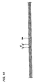
- Fig. 1 is a sectional view showing a conventional semiconductor device.
- a conventional semiconductor device 100 has a semiconductor chip 101, an internal connecting terminal 102, a resin layer 103, a wiring pattern 104, a solder resist 106, and an external connecting terminal 107.
- the semiconductor chip 101 has a semiconductor substrate 110 formed like a thin plate, a semiconductor integrated circuit 111, a plurality of electrode pads 112, and a protective film 113.
- the semiconductor integrated circuit 111 is provided on a surface side of the semiconductor substrate 110.
- the semiconductor integrated circuit 111 is constituted by a diffusion layer, an insulating layer and a wiring pattern (not shown).
- the electrode pads 112 are provided on the semiconductor integrated circuit 111.
- the electrode pads 112 are electrically connected to a wiring pattern provided on the semiconductor integrated circuit 111.
- the protective film 113 is provided on the semiconductor integrated circuit 111.
- the protective film 113 serves to protect the semiconductor integrated circuit 111.
- the internal connecting terminal 102 is provided on the electrode pad 112. An upper end of the internal connecting terminal 102 is exposed from the resin layer 103. The upper end of the internal connecting terminal 102 is connected to the wiring pattern 104.
- the resin layer 103 is provided to cover the semiconductor chip 101 on a side where the internal connecting terminal 102 is disposed.
- the wiring pattern 104 is provided on the resin layer 103.
- the wiring pattern 104 is connected to the internal connecting terminal 102.
- the wiring pattern 104 is electrically connected to the electrode pad 112 through the internal connecting terminal 102.
- the wiring pattern 104 has a pad 104A provided with an external connecting terminal 107.
- the solder resist 106 is provided on the resin layer 103 to cover the wiring pattern 104 in a portion excluding the pad 104A.
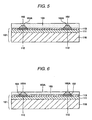
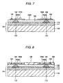
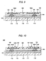
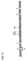
- Figs. 2 to 10 are views showing a process for manufacturing the conventional semiconductor device.
- the same components as those in the conventional semiconductor device 100 shown in Fig. 1 have the same reference numerals.
- the semiconductor chip 101 having the semiconductor integrated circuit 111, the electrode pads 112 and the protective film 113 on the surface side of the semiconductor substrate 110 which has not been formed into a thin plate.
- the internal connecting terminal 102 is formed on the electrode pads 112. In this stage, the internal connecting terminals 102 have a variation in a height.
- a flat plate 115 is pressed against the internal connecting terminals 102 to cause the heights of the internal connecting terminals 102 to be equal to each other. Consequently, upper surfaces 102A of the internal connecting terminals 102 are formed to be almost flat surfaces.
- the resin layer 103 is formed to cover the semiconductor chip 101 on the side where the internal connecting terminal 102 is formed and the internal connecting terminal 102.
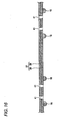
- the resin layer 103 is polished until the upper surface 102A of the internal connecting terminal 102 is exposed from the resin layer 103.
- the polishing is carried out in such a manner that an upper surface 103A of the resin layer 103 is almost on the level with the upper surface 102A of the internal connecting terminal 102. Consequently, an upper surface of the structure shown in Fig. 6 (more specifically, the upper surface 103A of the resin layer 103 and the upper surface 102A of the internal connecting terminal 102) is flat.
- the wiring pattern 104 is formed on the upper surface of the structure illustrated in Fig. 6 which is flat. More specifically, a metal foil (not shown) is stuck to the upper surface of the structure shown in Fig. 6 and a resist (not shown) is then applied to cover the metal foil, and subsequently, the resist is exposed and developed to form a resist film (not shown) on the metal foil in a part corresponding to the region in which the wiring pattern 104 is formed. Thereafter, the metal foil is etched by using the resist film as a mask so that the wiring pattern 104 is formed (a subtractive method). Then, the resist film is removed. An exposing region of the resist is determined by detecting a position of an alignment mark (not shown) formed on the semiconductor integrated circuit 111 through an exposing device (not shown) having infrared rays or an X-ray transmitting function.
- solder resist 106 covering the wiring pattern 104 in a portion other than the pad 104A is formed on the resin layer 103.
- the exposing device having the infrared rays or X-ray transmitting function which is to be used in the formation of the resist film for forming the wiring pattern 104 is expensive. For this reason, there is a problem in that the manufacturing cost of the semiconductor device 100 is increased.
- JP 2002 313985 discloses a method of manufacturing a chip size package.
- the method includes, among others, the step of preparing a semiconductor wafer with a plurality of semiconductor chip regions having integrated circuits and electrodes.
- a plurality of bumps connected with the plurality of electrodes is formed and a load is applied to level and to make uniform the height of the plurality of bumps.
- the semiconductor wafer is covered with a resin, and the resin is polished to expose the plurality of bumps.
- a plurality of solder balls is formed on the plurality of bumps.
- a method of manufacturing a semiconductor device including a plurality of semiconductor chips including an electrode pad, a semiconductor substrate having a plurality of semiconductor chip forming regions in which the semiconductor chips are formed, an internal connecting terminal provided on the electrode pad, and a wiring pattern which is electrically connected to the internal connecting terminal, the method including the steps of:
- the internal connecting terminal is formed on the electrode pad of the semiconductor chips, a through hole is formed in the support plate having a metal layer, which metal layer to be the base material of the wiring pattern is provided on a plate member, a conductive terminal is thereafter formed on the metal layer in an opposed part to the internal connecting terminal, the semiconductor chips and the support plate are subsequently disposed opposite to each other in such a manner that the internal connecting terminal and the conductive terminal are opposed to each other, and the support plate is pressed to pressure bond the internal connecting terminal to the metal layer, and a portion between the semiconductor chips and the support plate and the through hole are then sealed with a resin.
- the plate member is removed and thereby a protruded portion is formed of the resin in a corresponding part to the through hole of the support plate after the sealing step, the protruded portion is then used as an alignment mark to form a resist film covering the metal layer in a corresponding part to a region in which the wiring pattern is formed, and the metal layer is thereafter etched by using the resist film as a mask, thereby forming the wiring pattern. Consequently, it is possible to enhance precision in the position in which the wiring pattern is formed with respect to the internal connecting terminal.
- the resist film When forming the resist film, furthermore, it is possible to detect the position of the protruded portion to be the alignment mark by using an inexpensive exposing device including a CCD camera. Therefore, it is possible to reduce the manufacturing cost of the semiconductor device.
- a method of manufacturing a semiconductor device including a plurality of semiconductor chips including an electrode pad, a semiconductor substrate having a plurality of semiconductor chip forming regions in which the semiconductor chips are formed, an internal connecting terminal provided on the electrode pad, and a wiring pattern which is electrically connected to the internal connecting terminal, the method including the steps of:
- the internal connecting terminal is formed on the electrode pads of the semiconductor chips, through hole is formed in the support plate having a metal layer, which metal layer to be the base material of the wiring pattern is provided on a plate member, and a conductive terminal is thereafter formed on the metal layer in an opposed part to the internal connecting terminal, the semiconductor chips and the support plate are subsequently disposed opposite to each other in such a manner that the internal connecting terminal and the conductive terminal are opposed to each other, and the support plate is pressed to pressure bond the internal connecting terminal to the conductive terminal, and a portion between the semiconductor chips and the support plate and the penetrating portion are then sealed with a resin.
- the plate member is removed and a protruded portion is thereby formed of the resin in a corresponding part to the through hole of the support plate after the sealing step, the protruded portion is then used as an alignment mark to form a resist film having an opening portion in a corresponding part to a region in which the wiring pattern is to be formed on the metal layer, and a plated film is subsequently formed on the metal layer in an exposed part in the opening portion through an electrolytic plating method using the metal layer as a feeding layer, the resist film is then removed, and the metal layer in a part in which the plated film is not formed is thereafter removed to form the wiring pattern constituted by the metal layer and the plated film. Consequently, it is possible to enhance precision in a position in which the wiring pattern is formed with respect to the internal connecting terminal.
- an internal connecting terminal is formed on an electrode pad of a plurality of semiconductor chips formed on a semiconductor substrate, and there is formed a resin member having a resin member body and a protruded portion and covering the semiconductor chips on which the internal connecting terminal is formed, a metal layer is formed on the resin member body and the protruded portion is used as an alignment mark to form a resist film covering the metal layer in a part corresponding to a region in which a wiring pattern is to be formed and to then carry out etching over the metal layer by using the resist layer as a mask, thereby forming the wiring pattern which is electrically connected to the internal connecting terminal.
- the invention it is possible to reduce a manufacturing cost of the semiconductor device, and furthermore, to enhance precision in a position in which the wiring pattern is formed with respect to the internal connecting terminal.
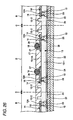
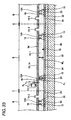
- FIG. 11 is a sectional view showing a semiconductor device made according to a first method of the invention.
- a semiconductor device 10 made according to the first method includes a semiconductor chip 11, an internal connecting terminal 12, a resin member 13, a wiring pattern 14, a conductive terminal 16, a solder resist 17, and an external connecting terminal 18.
- the semiconductor chip 11 includes a semiconductor substrate 21, a semiconductor integrated circuit 22, an electrode pad 23 and a protective film 24.
- the semiconductor substrate 21 serves to form the semiconductor integrated circuit 22 and is made thin.
- the semiconductor substrate 21 it is possible to use a substrate formed of silicon, for example.
- the semiconductor substrate 21 can be set to have a thickness of 100 ⁇ m to 300 ⁇ m, for example, in particular 150 ⁇ m to 250 ⁇ m.
- the semiconductor integrated circuit 22 is provided on a surface 21A side of the semiconductor substrate 21.
- the semiconductor integrated circuit 22 is constituted by a diffusion layer (not shown) formed on the semiconductor substrate 21, an insulating layer (not shown) laminated on the semiconductor substrate 21 and a wiring pattern (not shown) provided on the laminated insulating layer and connected electrically to the diffusion layer (not shown).
- a plurality of electrode pads 23 is provided on the semiconductor integrated circuit 22.
- the electrode pad 23 is electrically connected to the wiring pattern (not shown) provided on the semiconductor integrated circuit 22.
- the protective film 24 is provided on the semiconductor integrated circuit 22.
- the protective film 24 serves to protect the semiconductor integrated circuit 22.
- the protective film 24 it is possible to use an SiN film or a PSG film, for example.
- the internal connecting terminal 12 is provided on the electrode pad 23.
- the internal connecting terminal 12 serves to electrically connect the semiconductor integrated circuit 22 to the wiring pattern 14.
- An upper surface 12A of the upper end of the internal connecting terminal 12 is almost flat.
- the upper surface 12A of the upper end of the internal connecting terminal 12 is provided in contact with a lower surface of the wiring pattern 14. Consequently, the electrode pad 23 is electrically connected to the wiring pattern 14.
- the upper surface 12A of the upper end of the internal connecting terminal 12 is on almost the level with an upper surface 13-1A of a resin member body 13-1 (one of components of the resin member 13) which will be described below.
- the internal connecting terminal 12 can be set to have a height H 1 of 30 ⁇ m to 50 ⁇ m, for example, in particular 35 ⁇ m to 45 ⁇ m.
- the internal connecting terminal 12 it is possible to use a metal film constituted by an Au bump, an Au plated film, an Ni film formed by a nonelectrolytic plating method, and an Au film covering the Ni film, for example.
- the internal connecting terminal 12 can be formed by a bonding method or a plating method, for example.
- Fig. 12 is a plan view for explaining the resin member provided in the semiconductor device illustrated in Fig. 11 .
- the same components as those of the semiconductor device 10 illustrated in Fig. 11 have the same reference numerals.
- the resin member 13 has the resin member body 13-1 and a protruded portion 13-2.
- the resin member body 13-1 is provided to cover a side surface of the internal connecting terminal 12, an upper surface of the electrode pad 23 in a portion in which the internal connecting terminal 12 is not provided, and an upper surface of the protective film 24.
- the resin member body 13-1 takes a square shape seen on a plane.
- An upper surface 13-1A of the resin member body 13-1 is almost flat.
- the upper surface 13-1A of the resin member body 13-1 is almost on the level with the upper surface 12A of the upper end of the internal connecting terminal 12.
- the wiring pattern 14 is formed on the upper surface 13-1A of the resin member body 13-1.
- the resin member body 13-1 in a portion disposed between the solder resist 17 and the protective film 24 can be set to have a thickness M 1 of 30 ⁇ m to 50 ⁇ m, for example, in particular 35 ⁇ m to 45 ⁇ m.
- the protruded portion 13-2 takes a cylindrical shape and is provided on the upper surface 13-1A of the resin member body 13-1.
- the protruded portions 13-2 are disposed one by one in the vicinity of four corner portions of the resin member body 13-1.
- the protruded portion 13-2 is a member to be used as an alignment mark in a processing of exposing a resist film for patterning the wiring pattern 14 which will be described below.
- the protruded portion 13-2 can be set to have a diameter R 1 of 100 ⁇ m, for example.
- the protruded portion 13-2 can be set to have a height H 2 of 50 ⁇ m, for example.
- an underfill resin or a mold resin for example, an epoxy resin
- the protruded portion 13-2 By providing the protruded portion 13-2 on the upper surface 13-1A of the resin member body 13-1 on which the wiring pattern 14 is formed, thus, it is possible to use the protruded portion 13-2 as the alignment mark when executing the processing of exposing a resist film for patterning a metal layer to be a base material of the wiring pattern 14 (a metal layer formed on the upper surface 13-1A of the resin member body 13-1). Consequently, it is possible to enhance precision in a resist film forming position more greatly than that in the conventional art. Therefore, it is possible to enhance the precision in the position in which the wiring pattern 14 is formed with respect to the internal connecting terminal 12.
- the wiring pattern 14 is provided on the upper surface 13-1A of the resin member body 13-1 to come in contact with the upper surface 12A of the upper end of the internal connecting terminal 12.
- the wiring pattern 14 is electrically connected to the semiconductor integrated circuit 22 through the internal connecting terminal 12.
- the wiring pattern 14 has a pad portion 27.
- the pad portion 27 serves to provide the external connecting terminal 18 thereon and is disposed in a position placed apart from the internal connecting terminal 12.
- the wiring pattern 14 it is possible to use a Cu film, for example.
- the wiring pattern 14 can be set to have a thickness of 12 ⁇ m, for example.
- the conductive terminal 16 is provided on a lower surface of the wiring pattern 14 in an opposed part to the internal connecting terminal 12.
- the conductive terminal 16 is disposed to cover a side surface of the upper end of the internal connecting terminal 12.
- the conductive terminal 16 serves to fix the internal connecting terminal 12 to the wiring pattern 14.
- a conductive paste more specifically, for example, an Ag paste or a Cu paste
- a bump more specifically, for example, an Au bump or a Cu bump
- the solder resist 17 is provided on the resin member 13 to cover the wiring pattern 14 in a portion excluding the pad portion 27 and the protruded portion 13-2.
- the solder resist 17 has an opening portion 29 for exposing the pad portion 27 therefrom.
- the external connecting terminal 18 is provided on the pad portion 27.
- the external connecting terminal 18 is connected to an external connecting pad (not shown) provided on a mounting board (not shown) such as a mother board.
- a solder bump for example.
- the protruded portion 13-2 is provided on the upper surface 13-1A of the resin member body 13-1 on which the wiring pattern 14 is formed. Consequently, it is possible to use the protruded portion 13-2 as the alignment mark when executing the processing of exposing the resist film for patterning the metal layer to be the base material of the wiring pattern 14 (the metal layer formed on the upper surface 13-1A of the resin member body 13-1). Consequently, it is possible to enhance the precision in the resist film forming position more greatly than that in the conventional art. Therefore, it is possible to enhance the precision in the position in which the wiring pattern 14 is formed with respect to the internal connecting terminal 12.
- the resist film (not shown) for patterning the metal layer to be the base material of the wiring pattern 14 (the metal layer formed on the upper surface 13-1A of the resin member body 13-1)
- it is possible to detect the protruded portion 13-2 to be the alignment mark by using an inexpensive exposing apparatus (not shown) including a CCD camera (not shown). Therefore, it is possible to reduce a manufacturing cost of the semiconductor device 10.
- the four protruded portions 13-2 may be provided on the resin member body 13-1 in a corresponding part to a region other than the wiring pattern forming region in which the wiring pattern 14 is formed. In this case, it is possible to produce the same advantages as those in the semiconductor device 10 according to the embodiment.
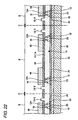
- Figs. 13 to 27 are views showing a process for manufacturing the semiconductor device according to the first method of the invention.
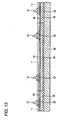
- Fig. 28 is a plan view for explaining a penetrating portion formed on a support having a metal layer.
- B denotes a region in which the semiconductor device 10 is formed (which will be hereinafter referred to as a “semiconductor device forming region B")
- C denotes a position in which a semiconductor substrate 35 is cut when dividing the semiconductor devices 10 into individual pieces (which will be hereinafter referred to as a "cutting position C").
- a method of manufacturing the semiconductor device according to Fig. 11 First of all, at the step shown in Fig. 13 , a plurality of semiconductor chips 11 having a semiconductor integrated circuit 22, an electrode pad 23 and a protective film 24 is formed on a semiconductor substrate 35 having a plurality of semiconductor chip forming regions, and an internal connecting terminal 12 is then formed on the electrode pad 23 (an internal connecting terminal forming step).
- the semiconductor substrate 35 is cut and divided into individual pieces at a step shown in Fig. 27 which will be described below and thus serves as the semiconductor substrate 21 described with reference to Fig. 11 .
- the semiconductor substrate 35 it is possible to use an Si wafer, for example.
- the semiconductor substrate 35 can be set to have a thickness of 500 ⁇ m to 775 ⁇ m, for example, in particular 550 ⁇ m to 650.
- a material of the electrode pad 23 it is possible to use Al or an Al alloy (for example, an Al - Si - Cu alloy).
- the protective film 24 it is possible to use an SiN film or a PSG film, for example.
- the internal connecting terminal 12 it is possible to use a metal film constituted by an Au bump, an Au plated film, an Ni film formed by a nonelectrolytic plating method, and an Au film covering the Ni film, for example.
- the internal connecting terminal 12 can be formed by a bonding method or a plating method, for example.
- the internal connecting terminals 12 have a variation in a height. In this stage, moreover, the upper surface of the upper end of the internal connecting terminal 12 is not flat.
- a support plate 37 having a metal layer in which a metal layer 39 to be the base material of the wiring pattern 14 is stuck to a surface 38A of a member plate 38 (a step of preparing a support plate having a metal layer).
- the metal layer 39 is stuck to the plate member plate 38 in a state in which it can be peeled from the plate member 38.
- the plate member 38 is a plate member capable of supporting the metal layer 39 and can easily be separated. More specifically, it is possible to use a metal plate (for example, a Cu plate), a metal foil (for example, a Cu foil) and a resin plate for the plate member 38, for example.
- the plate member 38 can be set to have a thickness of 35 ⁇ m, for example.
- the metal layer 39 it is possible to use the Cu layer, for example.
- the metal layer 39 can be set to have a thickness of 12 ⁇ m, for example.
- a through hole 41 is formed in the support plate 37 having a metal layer in an opposed part to a semiconductor chip 11 shown in Fig. 13 (a penetrating portion forming step).
- the penetrating portion 41 is formed in each support plate 37 having a metal layer in opposed parts of four corner portions in an external position A of the semiconductor chip 11 taking a square shape seen on a plane, for example.
- the penetrating portion 41 can be formed by a method such as a router processing, drilling or pressing, for example.
- the penetrating portion 41 For the shape of the penetrating portion 41, moreover, it is possible to use a shape of a cylinder, a square pole or a slit (a trench) (In Fig. 15 , the penetrating portion 41 taking a cylindrical shape is shown by taking an example.) In the case in which the penetrating portion 41 takes a cylindrical shape, the penetrating portion 41 can be set to have a diameter R 2 , for example, 100 ⁇ m.
- a conductive terminal 16 is formed on the metal layer 39 in the opposed part to the internal connecting terminal 12 provided in the structure shown in Fig. 13 (a conductive terminal forming step).
- a conductive paste more specifically, for example, an Ag paste or a Cu paste
- a bump more specifically, for example, an Au bump or a Cu bump
- the penetrating portion 41 formed in the support plate 37 having a metal layer is used as the alignment mark to dispose the semiconductor chips 11 formed on the semiconductor substrate 35 and the support plate 37 having a metal layer opposite to each other in such a manner that the internal connecting terminal 12 provided in the structure shown in Fig. 13 is opposed to the conductive terminal 16 provided in the structure shown in Fig. 16 .
- a heating temperature is 180°, for example, in the case in which the Au bump is used for the conductive terminal 16
- the support plate 37 having a metal layer is pressed in such a manner that the upper end of the internal connecting terminal 12 comes in contact with the metal layer 39 to pressure bond the internal connecting terminal 12 to the metal layer 39 (steps shown in Figs. 17 and 18 indicate the pressure bonding step).
- the internal connecting terminal 12 obtained after the pressure bonding step can be set to have a height H 1 of 30 ⁇ m to 50 ⁇ m, for example.
- a clearance between the protective film 24 and the metal layer 39 can be set to be 30 ⁇ m to 50 ⁇ m, for example.
- the penetrating portion 41 formed in the support plate 37 having a metal layer as the alignment mark when disposing the semiconductor chips 11 formed on the semiconductor substrate 35 and the support plate 37 having a metal layer opposite to each other, thus, it is possible to align the conductive terminal 16 with the internal connecting terminal 12 with high precision. Therefore, it is possible to enhance an electrical connecting reliability of the internal connecting terminal 12 and the metal layer 39 (the wiring pattern 14) in the portion in which the conductive terminal 16 is provided.
- a portion between the semiconductor chips 11 formed on the semiconductor substrate 35 and the support plate 37 having a metal layer and the penetrating portion 41 are sealed with a resin 46 (a sealing step).
- the resin 46 is a base material of the resin member 13 shown in Fig. 11 described above.
- the resin 46 it is possible to use an underfill resin or a mold resin (for example, an epoxy resin), for example.
- the resin 46 can be formed by a transfer mold method.
- the structure shown in Fig. 18 is accommodated between a lower metal mold 43 and an upper metal mold 44, and the resin 46 is then pressed into a portion between the lower metal mold 43 and the upper metal mold 44. Consequently, the portion between the semiconductor chips 11 and the support plate 37 having a metal layer and the penetrating portion 41 are sealed with the resin 46.
- the resin 46 is formed by using the transfer mold method
- a clearance is formed between the upper metal mold 44 and the plate member 38 so that the support plate 37 having a metal layer is not pressed by the upper metal mold 44. Therefore, it is possible to prevent the metal layer 39 to be the base material of the wiring pattern 14 from being flexed.
- the resin 46 is formed to cover an upper surface of the plate member 38.
- the case in which the resin 46 to be the base material of the resin member 13 is formed by the transfer mold method is taken as an example and is illustrated.
- the plate member 38 is peeled from the metal layer 39 provided in the structure shown in Fig. 20 , and the resin 46 formed on the plate member 38 is removed together with the plate member 38 so that the protruded portion 13-2 is formed (a protruded portion forming step). Consequently, the resin member 13 including the resin member body 13-1 and the protruded portion 13-2 is formed.
- a thickness M 1 of the resin member body 13-1 (a thickness of the resin member body 13-1 in a portion disposed between the protective film 24 and the metal layer 39) can be set to be 30 ⁇ m to 50 ⁇ m, for example.
- the protruded portions 13-2 are formed one by one in the vicinity of four corner portions of the resin member body 13-1.
- a diameter R 1 of the protruded portion 13-2 can be set to be 100 ⁇ m, for example.
- a height H 2 of the protruded portion 13-2 can be set to be 50 ⁇ m, for example.
- a protrusion amount E of the protruded portion 13-2 based on an upper surface 39A of the metal layer 39 can be set to be 38 ⁇ m, for example.
- the protruded portion 13-2 is used as the alignment mark to form a resist film 48 covering the metal layer 39 in a corresponding part to the region in which the wiring pattern 14 is formed (a resist film forming step).
- the resist film 48 serves as a mask for etching the metal layer 39.
- the resist film 48 is a positive resist
- the resist is applied onto the metal layer 39 and an inexpensive exposing device (not shown) including a CCD camera (not shown) is then used to detect the position of the protruded portion 13-2 to be the alignment mark, and a light is irradiated on the resist in the corresponding part to the region in which the wiring pattern 14 is formed to carry out an exposing treatment, and the resist obtained after the exposure is thereafter subjected to a developing treatment so that the resist film 48 is formed.
- the protruded portion 13-2 as the alignment mark when carrying out the exposing treatment over the resist film 48 for patterning the metal layer 39 to be the base material of the wiring pattern 14, thus, it is possible to enhance the precision in the position in which the resist film 48 is formed more greatly than that in the conventional art. Therefore, it is possible to enhance the precision in the position in which the wiring pattern 14 is formed with respect to the internal connecting terminal 12.
- the metal layer 39 shown in Fig. 22 is subjected to etching (more specifically, for example, anisotropic etching) by using the resist film 48 as a mask to form the wiring pattern 14 connected to the internal connecting terminal 12 (a wiring pattern forming step).
- etching more specifically, for example, anisotropic etching
- the wiring pattern 14 is formed by a subtractive method is taken as an example and is illustrated.
- the wiring pattern 14 has the pad portion 27 in which the external connecting terminal 18 is provided.
- a thickness of the wiring pattern 14 is almost equal to that of the metal layer 39.
- the thickness of the wiring pattern 14 can be set to be 12 ⁇ m, for example.
- the wiring pattern 14 in a portion excluding the pad portion 27 and the solder resist 17 covering the protruded portion 13-2 are formed on the upper surface 13-1A of the resin member body 13-1 by a well-known technique, and the external connecting terminal 18 is then formed on the pad portion 27.
- the solder resist 17 has the opening portion 29 for exposing the pad portion 27.
- the thickness of the semiconductor substrate 35 is reduced from a back face 35B side of the semiconductor substrate 35 shown in Fig. 25 . More specifically, the semiconductor substrate 35 is polished or ground from the back face 35B side of the semiconductor substrate 35, thereby changing the semiconductor substrate 35 into a thin plate. Consequently, a structure corresponding to the semiconductor device 10 is formed in the semiconductor device forming region B of the semiconductor substrate 35.
- a backside grinder In order to reduce the thickness of the semiconductor substrate 35, for example, it is possible to use a backside grinder.
- the thickness of the semiconductor substrate 35 obtained after reducing the thickness can be set to be 100 ⁇ m to 300 ⁇ m, for example, in particular 150 ⁇ m to 250 ⁇ m.
- a portion corresponding to the cutting position C of the structure shown in Fig. 26 is cut. Consequently, the structure is divided into individual pieces so that the semiconductor devices 10 are manufactured.
- the protruded portion 13-2 as the alignment mark when carrying out the exposing treatment over the resist film 48 serving as the mask for patterning the metal layer 39 to be the base material of the wiring pattern 14, moreover, it is possible to enhance the precision in the position in which the resist film 48 is formed more greatly than that in the conventional art. Therefore, it is possible to enhance the precision in the position in which the wiring pattern 14 is formed with respect to the internal connecting terminal 12.
- the resist film 48 serving as a mask for patterning the metal layer 39 to be the base material of the wiring pattern 14 furthermore, it is possible to detect the position of the protruded portion 13-2 serving as the alignment mark by using an inexpensive exposing device (not shown) including a CCD camera (not shown). Therefore, it is possible to reduce the manufacturing cost of the semiconductor device 10.
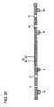
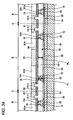
- Fig. 29 is a sectional view showing a semiconductor device made according to a second method of the invention.
- the same components as those in the semiconductor device 10 made according to the first method have the same reference numerals.
- a semiconductor device 50 made according to the second method has the same structure as that of the semiconductor device 10 except that a wiring pattern 51 is provided in place of the wiring pattern 14 disposed in the semiconductor device 10 according to the first embodiment (a wiring pattern formed by using a subtractive method).
- the wiring pattern 51 has such a structure that a metal layer 54 and a plated film 55 are laminated.
- the wiring pattern 51 has a pad portion 52 on which an external connecting terminal 18 is provided.
- the metal layer 54 is provided on an upper surface 12A of an upper end of an internal connecting terminal 12 and an upper surface 13-1A of a resin member body 13-1.
- a lower surface of the metal layer 54 is provided in contact with the upper surface 12A of the upper end of the internal connecting terminal 12.
- the lower surface of the metal layer 54 is provided with a conductive terminal 16 for connecting the internal connecting terminal 12 to the metal layer 54.
- the metal layer 54 is a feeding layer for forming the plated film 55.
- the metal layer 54 it is possible to use a Cu layer, for example. In the case in which the Cu layer is used as the metal layer 54, the metal layer 54 can be set to have a thickness of 2 ⁇ m to 3 ⁇ m, for example.
- the plated film 55 is laminated on the metal layer 54.
- the plated film 55 it is possible to use a Cu plated film, for example.
- the plated film 55 can be set to have a thickness of 10 ⁇ m, for example.
- the plated film 55 can be formed by an electrolytic method, for example.
- the wiring pattern 51 having the structure can be formed by a semiadditive method, for example.
- the semiconductor device 50 according to the second embodiment having the structure can produce the same advantages as those of the semiconductor device 10 according to the first embodiment.
- Figs. 30 to 37 are views showing a process for manufacturing the semiconductor device according to the second embodiment of the invention.
- the same components as those in the semiconductor device 50 according to the second embodiment have the same reference numerals.
- a method of manufacturing the semiconductor device 50 according to Fig. 29 First of all, the same step as that shown in Fig. 13 described in the first embodiment is carried out to form a plurality of semiconductor chips 11 having a semiconductor integrated circuit 22, an electrode pad 23 and a protective film 24 on a semiconductor substrate 35 having a plurality of semiconductor chip forming regions and to then form an internal connecting terminal 12 on the electrode pad 23 (an internal connecting terminal forming step).
- the support plate 57 having a metal layer in which the metal layer 54 serving as a feeding layer for forming the plated film 55 (see Fig. 29 ) is stuck to a surface 38A of a plate member 38 (a step of preparing a support plate having a metal layer).
- the metal layer 54 is stuck to the plate member 38 in a state in which it can be peeled from the plate member 38. It is sufficient that the plate member 38 can support the metal layer 54. More specifically, it is possible to use a metal plate (for example, a Cu plate), a metal foil (for example, a Cu foil) and a resin plate for the plate member 38, for example.
- the plate member 38 can be set to have a thickness of 35 ⁇ m, for example.
- a Cu layer can be used, for example.
- the metal layer 54 can be set to have a thickness of 2 ⁇ m to 3 ⁇ m, for example.
- a penetrating portion 41 i.e. a through hole, is formed in the support plate 57 having a metal layer in the opposed part to the semiconductor chip 11 shown in Fig. 13 described in the first embodiment (a penetrating portion forming step).
- the penetrating portions 41 are formed one by one on the support plates 57 having metal layers in opposed parts to four corner portions of an external position A of the semiconductor chip 11 taking a square shape seen on a plane, for example.
- the penetrating portion 41 can be formed by using a method such as a router processing, drilling or pressing.
- a shape of the penetrating portion 41 moreover, it is possible to use a shape of a cylinder, a square pole or a slit (a trench).
- a diameter R 2 of the penetrating portion 41 can be set to be 100 ⁇ m, for example.
- the conductive terminal 16 is formed on the metal layer 54 in the opposed part to the internal connecting terminal 12 provided in the structure shown in Fig. 13 described in the first embodiment (a conductive terminal forming step).
- a conductive terminal forming step it is possible to use a conductive paste (more specifically, for example, an Ag paste or a Cu paste) or a bump (more specifically, for example, an Au bump or a Cu bump), for example.
- a height H 1 of the internal connecting terminal 12 which is obtained after the pressure bonding step can be set to be 30 ⁇ m to 50 ⁇ m, for example.
- a clearance between the protective film 24 and the metal layer 54 can be set to be 30 ⁇ m to 50 ⁇ m, for example.
- a thickness M 1 of the resin member body 13-1 can be set to be 30 ⁇ m to 50 ⁇ m, for example.
- Protruded portions 13-2 are disposed one by one in the vicinity of the four corner portions of the resin member body 13-1.
- a diameter R 1 of the protruded portion 13-2 can be set to be 100 ⁇ m, for example.
- a height H 2 of the protruded portion 13-2 can be set to be 50 ⁇ m, for example.
- a protrusion amount E of the protruded portion 13-2 based on an upper surface 54A of the metal layer 54 can be set to be 48 ⁇ m, for example.
- the protruded portion 13-2 is used as an alignment mark to form, on a resin member 13 and the metal layer 54, a resist film 61 having an opening portion 61A in a corresponding part to the region in which the wiring pattern 51 is to be formed (more specifically, the region in which the plated film 55 to be one of components of the wiring pattern 51 is formed) (a resist film forming method).
- the resist film 61 is a positive resist
- the resist film 61 having the opening portion 61A is formed by irradiating a light on a resist in the corresponding part to the region in which the wiring pattern 51 is to be formed to carry out an exposing treatment by using the protruded portion 13-2 to be the alignment mark through an inexpensive exposing device (not shown) including a CCD camera (not shown) when applying the resist and then performing the exposing treatment through an exposing device (not shown) and then executing a developing treatment over the resist obtained after the exposure.
- the resist film 61 is a mask for forming the plated film 55 on only the metal layer 54 in the corresponding part to the region in which the wiring pattern 51 is to be formed.
- the protruded portion 13-2 as the alignment mark when executing the exposing treatment over the resist film 61 for patterning the metal layer 54 to be the base material of the wiring pattern 51, thus, it is possible to enhance precision in the position in which the opening portion 61A of the resist film 61 formed in the corresponding part to the region in which the wiring pattern 51 is to be formed (more specifically, the region in which the plated film 55 to be one of the components of the wiring pattern 51 is formed). Therefore, it is possible to enhance precision in the position in which the wiring pattern 51 is to be formed with respect to the internal connecting terminal 12.
- the resist film 61 serving as a mask for patterning the metal layer 54 to be the base material of the wiring pattern 51 furthermore, it is possible to detect the position of the protruded portion 13-2 serving as the alignment mark by using an inexpensive exposing device (not shown) including a CCD camera (not shown). Therefore, it is possible to reduce the manufacturing cost of the semiconductor device 50.
- the plated film 55 is formed on the metal layer 54 in an exposed part to the opening portion 61A through an electrolytic plating method using the metal layer 54 as a feeding layer (a plated film forming step).
- a plated film forming step it is possible to use a Cu plated film, for example.
- the plated film 55 can be set to have a thickness of 10 ⁇ m, for example.
- a step shown in Fig. 36 next, the resist film 61 shown in Fig. 35 is removed (a resist film removing step).
- a step shown in Fig. 37 subsequently, the metal layer 54 in a portion in which the plated film 55 is not formed is removed, and the wiring pattern 51 constituted by the metal layer 54 and the plated film 55 is formed (a wiring pattern forming step).
- the protruded portion 13-2 is used as the alignment mark for carrying out the exposing treatment over the resist film 61 for patterning the metal layer 54 to be the base material of the wiring pattern 51. Consequently, it is possible to enhance precision in the position in which the opening portion 61A of the resist film 61 is formed in the corresponding part to the region in which the wiring pattern 51 is formed (more specifically, the region in which the plated film 55 to be one of the components of the wiring pattern 51 is formed). Therefore, it is possible to enhance the precision in the position in which the wiring pattern 51 is formed with respect to the internal connecting terminal 12.
- the resist film 61 serving as the mask for patterning the metal layer 54 to be the base material of the wiring pattern 51 moreover, it is possible to detect the position of the protruded portion 13-2 to be the alignment mark by using an inexpensive exposing device (not shown) including a CCD camera (not shown). Therefore, it is possible to reduce the manufacturing cost of the semiconductor device 50.
- the invention can be applied to a method of manufacturing a semiconductor device including a semiconductor chip including an electrode pad, an internal connecting terminal provided on the electrode pad, and a wiring pattern which is electrically connected to the internal connecting terminal.
Description
- The present invention relates to a method of manufacturing a semiconductor device, and more particularly to a method of manufacturing a semiconductor device including a semiconductor chip including an electrode pad, an internal connecting terminal provided on the electrode pad, and a wiring pattern which is electrically connected to the internal connecting terminal.
- A conventional chip size package (for example, see
Fig. 1 ) includes a semiconductor device including an electrode pad, an internal connecting terminal provided on the electrode pad, and a wiring pattern which is electrically connected to the internal connecting terminal, and has an almost equal size to the size of the semiconductor chip as seen on a plane. -
Fig. 1 is a sectional view showing a conventional semiconductor device. - Referring to
Fig. 1 , aconventional semiconductor device 100 has asemiconductor chip 101, aninternal connecting terminal 102, aresin layer 103, awiring pattern 104, asolder resist 106, and anexternal connecting terminal 107. - The
semiconductor chip 101 has asemiconductor substrate 110 formed like a thin plate, a semiconductor integratedcircuit 111, a plurality ofelectrode pads 112, and aprotective film 113. The semiconductor integratedcircuit 111 is provided on a surface side of thesemiconductor substrate 110. The semiconductor integratedcircuit 111 is constituted by a diffusion layer, an insulating layer and a wiring pattern (not shown). Theelectrode pads 112 are provided on the semiconductor integratedcircuit 111. Theelectrode pads 112 are electrically connected to a wiring pattern provided on the semiconductor integratedcircuit 111. Theprotective film 113 is provided on the semiconductor integratedcircuit 111. Theprotective film 113 serves to protect the semiconductor integratedcircuit 111. - The internal connecting
terminal 102 is provided on theelectrode pad 112. An upper end of the internal connectingterminal 102 is exposed from theresin layer 103. The upper end of the internal connectingterminal 102 is connected to thewiring pattern 104. Theresin layer 103 is provided to cover thesemiconductor chip 101 on a side where the internal connectingterminal 102 is disposed. - The
wiring pattern 104 is provided on theresin layer 103. Thewiring pattern 104 is connected to theinternal connecting terminal 102. Thewiring pattern 104 is electrically connected to theelectrode pad 112 through theinternal connecting terminal 102. Thewiring pattern 104 has apad 104A provided with an externalconnecting terminal 107. Thesolder resist 106 is provided on theresin layer 103 to cover thewiring pattern 104 in a portion excluding thepad 104A. -
Figs. 2 to 10 are views showing a process for manufacturing the conventional semiconductor device. InFigs. 2 to 10 , the same components as those in theconventional semiconductor device 100 shown inFig. 1 have the same reference numerals. - First of all, at a step shown in
Fig. 2 , there is formed thesemiconductor chip 101 having the semiconductor integratedcircuit 111, theelectrode pads 112 and theprotective film 113 on the surface side of thesemiconductor substrate 110 which has not been formed into a thin plate. At a step shown inFig. 3 , next, the internal connectingterminal 102 is formed on theelectrode pads 112. In this stage, theinternal connecting terminals 102 have a variation in a height. - At a step shown in
Fig. 4 , subsequently, aflat plate 115 is pressed against theinternal connecting terminals 102 to cause the heights of the internal connectingterminals 102 to be equal to each other. Consequently,upper surfaces 102A of theinternal connecting terminals 102 are formed to be almost flat surfaces. At a step shown inFig. 5 , then, theresin layer 103 is formed to cover thesemiconductor chip 101 on the side where the internal connectingterminal 102 is formed and the internal connectingterminal 102. - At a step shown in
Fig. 6 , next, theresin layer 103 is polished until theupper surface 102A of the internal connectingterminal 102 is exposed from theresin layer 103. At this time, the polishing is carried out in such a manner that anupper surface 103A of theresin layer 103 is almost on the level with theupper surface 102A of the internal connectingterminal 102. Consequently, an upper surface of the structure shown inFig. 6 (more specifically, theupper surface 103A of theresin layer 103 and theupper surface 102A of the internal connecting terminal 102) is flat. - At a step shown in
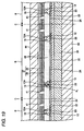
Fig. 7 , then, thewiring pattern 104 is formed on the upper surface of the structure illustrated inFig. 6 which is flat. More specifically, a metal foil (not shown) is stuck to the upper surface of the structure shown inFig. 6 and a resist (not shown) is then applied to cover the metal foil, and subsequently, the resist is exposed and developed to form a resist film (not shown) on the metal foil in a part corresponding to the region in which thewiring pattern 104 is formed. Thereafter, the metal foil is etched by using the resist film as a mask so that thewiring pattern 104 is formed (a subtractive method). Then, the resist film is removed. An exposing region of the resist is determined by detecting a position of an alignment mark (not shown) formed on the semiconductor integratedcircuit 111 through an exposing device (not shown) having infrared rays or an X-ray transmitting function. - At a step shown in
Fig. 8 , subsequently, the solder resist 106 covering thewiring pattern 104 in a portion other than thepad 104A is formed on theresin layer 103. - At a step shown in
Fig. 9 , next, thesemiconductor substrate 110 is polished from the back side of thesemiconductor substrate 110 so that thesemiconductor substrate 110 is made thin. At a step shown inFig. 10 , then, the external connectingterminal 107 is formed on thepad 104A. Consequently, thesemiconductor device 100 is manufactured (for example, see Patent Document 1). [Patent Document 1] Japanese Patent No.3614828 - In the method of manufacturing the
conventional semiconductor device 100, however, it is necessary to provide the step of causing the heights of the internal connectingterminals 102 to be equal to each other and the step of polishing theresin layer 103 to expose theupper surfaces 102A of theinternal connecting terminals 102 from theresin layer 103. For this reason, there is a problem in that a manufacturing cost of thesemiconductor device 100 is increased with an increase in the number of the steps. - Moreover, the exposing device having the infrared rays or X-ray transmitting function which is to be used in the formation of the resist film for forming the
wiring pattern 104 is expensive. For this reason, there is a problem in that the manufacturing cost of thesemiconductor device 100 is increased. - In the case in which the exposing device having the infrared rays or X-ray transmitting function is used, furthermore, precision in the detection of the alignment mark is not sufficient. For this reason, there is a problem in that precision in the position of the
wiring pattern 104 with respect to the internal connectingterminal 102 is reduced. - Further,
JP 2002 313985 - In light of the above, the method of manufacturing a semiconductor device according to independent claim 1, and the method according to independent claim 2 are provided. Further advantages, features, aspects and details are evident from the dependent claims, the description and the drawings.
In consideration of the problems, therefore, it is an object of the invention to provide a method of manufacturing a semiconductor device which can reduce a manufacturing cost of the semiconductor device and can enhance precision in a position of a wiring pattern with respect to an internal connecting terminal. - According to a first aspect of the invention, there is provided a method of manufacturing a semiconductor device including a plurality of semiconductor chips including an electrode pad, a semiconductor substrate having a plurality of semiconductor chip forming regions in which the semiconductor chips are formed, an internal connecting terminal provided on the electrode pad, and a wiring pattern which is electrically connected to the internal connecting terminal, the method including the steps of:
- forming the internal connecting terminal on the electrode pad of the semiconductor chips;
- preparing a support plate having a metal layer in which step a metal layer to be a base material of the wiring pattern is provided on a plate member;
- forming a through hole in the support plate in a part that will be opposite to the semiconductor chips;
- forming a conductive terminal on the metal layer in a part that will be opposite to the internal connecting terminal;
- disposing the semiconductor chips and the support plate opposite to each other in such a manner that the internal connecting terminal and the conductive terminal are opposed to each other and pressing the support plate to pressure bond the internal connecting terminal to the metal layer;
- sealing a portion between the semiconductor chips and the support plate and the through hole with a resin after the pressure bonding step;
- removing the plate member and thereby forming a protruded portion of the resin in a part corresponding to the through hole of the support plate after the sealing step;
- forming a resist film covering the metal layer in a part corresponding to a region in which the wiring pattern is to be formed by using the protruded portion as an alignment mark; and
- etching the metal layer by using the resist film as a mask to form the wiring pattern.
- According to features of the invention, the internal connecting terminal is formed on the electrode pad of the semiconductor chips, a through hole is formed in the support plate having a metal layer, which metal layer to be the base material of the wiring pattern is provided on a plate member, a conductive terminal is thereafter formed on the metal layer in an opposed part to the internal connecting terminal, the semiconductor chips and the support plate are subsequently disposed opposite to each other in such a manner that the internal connecting terminal and the conductive terminal are opposed to each other, and the support plate is pressed to pressure bond the internal connecting terminal to the metal layer, and a portion between the semiconductor chips and the support plate and the through hole are then sealed with a resin. Therefore, it is not necessary to provide a step of causing heights of the internal connecting terminals to be equal to each other and a resin polishing step of exposing the internal connecting terminal in a part connected to the wiring pattern from the resin. Consequently, it is possible to decrease the number of the steps. Thus, it is possible to reduce a manufacturing cost of the semiconductor device.
- Moreover, the plate member is removed and thereby a protruded portion is formed of the resin in a corresponding part to the through hole of the support plate after the sealing step, the protruded portion is then used as an alignment mark to form a resist film covering the metal layer in a corresponding part to a region in which the wiring pattern is formed, and the metal layer is thereafter etched by using the resist film as a mask, thereby forming the wiring pattern. Consequently, it is possible to enhance precision in the position in which the wiring pattern is formed with respect to the internal connecting terminal.
- When forming the resist film, furthermore, it is possible to detect the position of the protruded portion to be the alignment mark by using an inexpensive exposing device including a CCD camera. Therefore, it is possible to reduce the manufacturing cost of the semiconductor device.
- According to a sixth aspect of the invention, there is provided a method of manufacturing a semiconductor device including a plurality of semiconductor chips including an electrode pad, a semiconductor substrate having a plurality of semiconductor chip forming regions in which the semiconductor chips are formed, an internal connecting terminal provided on the electrode pad, and a wiring pattern which is electrically connected to the internal connecting terminal, the method including the steps of:
- forming the internal connecting terminal on the electrode pad of the semiconductor chips;
- preparing a support plate having a metal layer in which step the metal layer is provided on a plate member;
- forming a through hole in the support plate in a part that will be opposite to the semiconductor chips;
- forming a conductive terminal on the metal layer in a part that will be opposite to the internal connecting terminal;
- disposing the semiconductor chips and the support plate opposite to each other in such a manner that the internal connecting terminal and the conductive terminal are opposed to each other and pressing the support plate to pressure bond the internal connecting terminal to the metal layer;
- sealing a portion between the semiconductor chips and the support plate and the through hole with a resin after the pressure bonding step;
- removing the plate member and thereby forming a protruded portion of the resin in a part corresponding to the through hole of the support plate after the sealing step;
- forming a resist film having an opening portion in a part corresponding to a region in which the wiring pattern is to be formed on the metal layer by using the protruded portion as an alignment mark;
- forming a plated film on the metal layer in an exposed part in the opening portion by an electrolytic plating method using the metal layer as a feeding layer;
- removing the resist film after the plated film forming step; and
- removing the metal layer in a part in which the plated film is not formed to form the wiring pattern constituted by the metal layer and the plated film.
- According to features of the sixth aspect of the invention, the internal connecting terminal is formed on the electrode pads of the semiconductor chips, through hole is formed in the support plate having a metal layer, which metal layer to be the base material of the wiring pattern is provided on a plate member, and a conductive terminal is thereafter formed on the metal layer in an opposed part to the internal connecting terminal, the semiconductor chips and the support plate are subsequently disposed opposite to each other in such a manner that the internal connecting terminal and the conductive terminal are opposed to each other, and the support plate is pressed to pressure bond the internal connecting terminal to the conductive terminal, and a portion between the semiconductor chips and the support plate and the penetrating portion are then sealed with a resin. Therefore, it is not necessary to provide a step of causing heights of the internal connecting terminals to be equal to each other and a resin polishing step of exposing the internal connecting terminal in a portion connected to the wiring pattern from the resin. Consequently, it is possible to decrease the number of the steps. Thus, it is possible to reduce a manufacturing cost of the semiconductor device.
- Moreover, the plate member is removed and a protruded portion is thereby formed of the resin in a corresponding part to the through hole of the support plate after the sealing step, the protruded portion is then used as an alignment mark to form a resist film having an opening portion in a corresponding part to a region in which the wiring pattern is to be formed on the metal layer, and a plated film is subsequently formed on the metal layer in an exposed part in the opening portion through an electrolytic plating method using the metal layer as a feeding layer, the resist film is then removed, and the metal layer in a part in which the plated film is not formed is thereafter removed to form the wiring pattern constituted by the metal layer and the plated film. Consequently, it is possible to enhance precision in a position in which the wiring pattern is formed with respect to the internal connecting terminal.
- When forming the resist film, furthermore, it is possible to detect the position of the protruded portion to be the alignment mark by using an inexpensive exposing device including a CCD camera. Therefore, it is possible to reduce the manufacturing cost of the semiconductor device.
In one embodiment, an internal connecting terminal is formed on an electrode pad of a plurality of semiconductor chips formed on a semiconductor substrate, and there is formed a resin member having a resin member body and a protruded portion and covering the semiconductor chips on which the internal connecting terminal is formed, a metal layer is formed on the resin member body and the protruded portion is used as an alignment mark to form a resist film covering the metal layer in a part corresponding to a region in which a wiring pattern is to be formed and to then carry out etching over the metal layer by using the resist layer as a mask, thereby forming the wiring pattern which is electrically connected to the internal connecting terminal. - According to the invention, it is possible to reduce a manufacturing cost of the semiconductor device, and furthermore, to enhance precision in a position in which the wiring pattern is formed with respect to the internal connecting terminal.
- So that the manner in which the above recited features of the present invention can be understood in detail, a more particular description of the invention, briefly summarized above, may be had by reference to embodiments. The accompanying drawings relate to embodiments of the invention and are described in the following:
-
Fig. 1 is a sectional view showing a conventional semiconductor device. -
Fig. 2 is a view (No. 1) showing a step of manufacturing the conventional semiconductor device. -
Fig. 3 is a view (No. 2) showing the step of manufacturing the conventional semiconductor device. -
Fig. 4 is a view (No. 3) showing the step of manufacturing the conventional semiconductor device. -
Fig. 5 is a view (No. 4) showing the step of manufacturing the conventional semiconductor device. -
Fig. 6 is a view (No. 5) showing the step of manufacturing the conventional semiconductor device. -
Fig. 7 is a view (No. 6) showing the step of manufacturing the conventional semiconductor device. -
Fig. 8 is a view (No. 7) showing the step of manufacturing the conventional semiconductor device. -
Fig. 9 is a view (No. 8) showing the step of manufacturing the conventional semiconductor device. -
Fig. 10 is a view (No. 9) showing the step of manufacturing the conventional semiconductor device. -
Fig. 11 is a sectional view showing a semiconductor device manufactured according to a first method of the invention. -
Fig. 12 is a plan view for explaining a resin member provided in the semiconductor device illustrated inFig. 11 . -
Fig. 13 is a view (No. 1) showing a step of manufacturing the semiconductor device according to the first method of the invention. -
Fig. 14 is a view (No. 2) showing the step of manufacturing the semiconductor device according to the first method of the invention. -
Fig. 15 is a view (No. 3) showing the step of manufacturing the semiconductor device according to the first method of the invention. -
Fig. 16 is a view (No. 4) showing the step of manufacturing the semiconductor device according to the first method of the invention. -
Fig. 17 is a view (No. 5) showing the step of manufacturing the semiconductor device according to the first method of the invention. -
Fig. 18 is a view (No. 6) showing the step of manufacturing the semiconductor device according to the first method of the invention. -
Fig. 19 is a view (No. 7) showing the step of manufacturing the semiconductor device according to the first method of the invention. -
Fig. 20 is a view (No. 8) showing the step of manufacturing the semiconductor device according to the first method of the invention. -
Fig. 21 is a view (No. 9) showing the step of manufacturing the semiconductor device according to the first method of the invention. -
Fig. 22 is a view (No. 10) showing the step of manufacturing the semiconductor device according to the first method of the invention. -
Fig. 23 is a view (No. 11) showing the step of manufacturing the semiconductor device according to the first method of the invention. -
Fig. 24 is a view (No. 12) showing the step of manufacturing the semiconductor device according to the first method of the invention. -
Fig. 25 is a view (No. 13) showing the step of manufacturing the semiconductor device according to the first method of the invention. -
Fig. 26 is a view (No. 14) showing the step of manufacturing the semiconductor device according to the first method of the invention. -
Fig. 27 is a view (No. 15) showing the step of manufacturing the semiconductor device according to the first method of the invention. -
Fig. 28 is a plan view for explaining a penetrating portion formed on a support plate having a metal layer. -
Fig. 29 is a sectional view showing a semiconductor device manufactured according to a second method of the invention. -
Fig. 30 is a view (No. 1) showing a step of manufacturing the semiconductor device according to the second method of the invention. -
Fig. 31 is a view (No. 2) showing the step of manufacturing the semiconductor device according to the second method of the invention. -
Fig. 32 is a view (No. 3) showing the step of manufacturing the semiconductor device according to the second method of the invention. -
Fig. 33 is a view (No. 4) showing the step of manufacturing the semiconductor device according to the second method of the invention. -
Fig. 34 is a view (No. 5) showing the step of manufacturing the semiconductor device according to the second method of the invention. -
Fig. 35 is a view (No. 6) showing the step of manufacturing the semiconductor device according to the second method of the invention. -
Fig. 36 is a view (No. 7) showing the step of manufacturing the semiconductor device according to the second method of the invention. -
Fig. 37 is a view (No. 8) showing the step of manufacturing the semiconductor device according to the second method of the invention. - Next, a method according to the invention will be described with reference to the drawings.
- (First Embodiment)
Fig. 11 is a sectional view showing a semiconductor device made according to a first method of the invention. - Referring to
Fig. 11 , asemiconductor device 10 made according to the first method includes asemiconductor chip 11, an internal connectingterminal 12, aresin member 13, awiring pattern 14, aconductive terminal 16, a solder resist 17, and an external connectingterminal 18. - The
semiconductor chip 11 includes asemiconductor substrate 21, a semiconductor integratedcircuit 22, anelectrode pad 23 and aprotective film 24. Thesemiconductor substrate 21 serves to form the semiconductor integratedcircuit 22 and is made thin. For thesemiconductor substrate 21, it is possible to use a substrate formed of silicon, for example. Thesemiconductor substrate 21 can be set to have a thickness of 100µm to 300µm, for example, in particular 150µm to 250µm. - The semiconductor integrated
circuit 22 is provided on asurface 21A side of thesemiconductor substrate 21. The semiconductor integratedcircuit 22 is constituted by a diffusion layer (not shown) formed on thesemiconductor substrate 21, an insulating layer (not shown) laminated on thesemiconductor substrate 21 and a wiring pattern (not shown) provided on the laminated insulating layer and connected electrically to the diffusion layer (not shown). - A plurality of
electrode pads 23 is provided on the semiconductor integratedcircuit 22. Theelectrode pad 23 is electrically connected to the wiring pattern (not shown) provided on the semiconductor integratedcircuit 22. As a material of theelectrode pad 23, for example, it is possible to use Al or an Al alloy (such as an Al - Si - Cu alloy). - The
protective film 24 is provided on the semiconductor integratedcircuit 22. Theprotective film 24 serves to protect the semiconductor integratedcircuit 22. For theprotective film 24, it is possible to use an SiN film or a PSG film, for example. - The internal connecting
terminal 12 is provided on theelectrode pad 23. The internal connectingterminal 12 serves to electrically connect the semiconductor integratedcircuit 22 to thewiring pattern 14. Anupper surface 12A of the upper end of the internal connectingterminal 12 is almost flat. Theupper surface 12A of the upper end of the internal connectingterminal 12 is provided in contact with a lower surface of thewiring pattern 14. Consequently, theelectrode pad 23 is electrically connected to thewiring pattern 14.
Moreover, theupper surface 12A of the upper end of the internal connectingterminal 12 is on almost the level with an upper surface 13-1A of a resin member body 13-1 (one of components of the resin member 13) which will be described below. The internal connectingterminal 12 can be set to have a height H1 of 30µm to 50µm, for example, in particular 35µm to 45µm. - For the internal connecting
terminal 12, it is possible to use a metal film constituted by an Au bump, an Au plated film, an Ni film formed by a nonelectrolytic plating method, and an Au film covering the Ni film, for example. In the case in which the Au bump is used as the internal connectingterminal 12, the internal connectingterminal 12 can be formed by a bonding method or a plating method, for example. -
Fig. 12 is a plan view for explaining the resin member provided in the semiconductor device illustrated inFig. 11 . InFig. 12 , the same components as those of thesemiconductor device 10 illustrated inFig. 11 have the same reference numerals. - With reference to
Figs. 11 and12 , theresin member 13 has the resin member body 13-1 and a protruded portion 13-2. The resin member body 13-1 is provided to cover a side surface of the internal connectingterminal 12, an upper surface of theelectrode pad 23 in a portion in which the internal connectingterminal 12 is not provided, and an upper surface of theprotective film 24. The resin member body 13-1 takes a square shape seen on a plane. An upper surface 13-1A of the resin member body 13-1 is almost flat. The upper surface 13-1A of the resin member body 13-1 is almost on the level with theupper surface 12A of the upper end of the internal connectingterminal 12. Thewiring pattern 14 is formed on the upper surface 13-1A of the resin member body 13-1. The resin member body 13-1 in a portion disposed between the solder resist 17 and theprotective film 24 can be set to have a thickness M1 of 30µm to 50µm, for example, in particular 35µm to 45µm. - The protruded portion 13-2 takes a cylindrical shape and is provided on the upper surface 13-1A of the resin member body 13-1. The protruded portions 13-2 are disposed one by one in the vicinity of four corner portions of the resin member body 13-1. The protruded portion 13-2 is a member to be used as an alignment mark in a processing of exposing a resist film for patterning the
wiring pattern 14 which will be described below. The protruded portion 13-2 can be set to have a diameter R1 of 100µm, for example. Moreover, the protruded portion 13-2 can be set to have a height H2 of 50µm, for example. For theresin member 13 having the structure, it is possible to use an underfill resin or a mold resin (for example, an epoxy resin), for example. - By providing the protruded portion 13-2 on the upper surface 13-1A of the resin member body 13-1 on which the
wiring pattern 14 is formed, thus, it is possible to use the protruded portion 13-2 as the alignment mark when executing the processing of exposing a resist film for patterning a metal layer to be a base material of the wiring pattern 14 (a metal layer formed on the upper surface 13-1A of the resin member body 13-1). Consequently, it is possible to enhance precision in a resist film forming position more greatly than that in the conventional art. Therefore, it is possible to enhance the precision in the position in which thewiring pattern 14 is formed with respect to the internal connectingterminal 12. - The
wiring pattern 14 is provided on the upper surface 13-1A of the resin member body 13-1 to come in contact with theupper surface 12A of the upper end of the internal connectingterminal 12. Thewiring pattern 14 is electrically connected to the semiconductor integratedcircuit 22 through the internal connectingterminal 12. Thewiring pattern 14 has apad portion 27. Thepad portion 27 serves to provide the external connectingterminal 18 thereon and is disposed in a position placed apart from the internal connectingterminal 12. For thewiring pattern 14, it is possible to use a Cu film, for example. In the case in which the Cu film is used as thewiring pattern 14, thewiring pattern 14 can be set to have a thickness of 12µm, for example. - The
conductive terminal 16 is provided on a lower surface of thewiring pattern 14 in an opposed part to the internal connectingterminal 12. Theconductive terminal 16 is disposed to cover a side surface of the upper end of the internal connectingterminal 12. Theconductive terminal 16 serves to fix the internal connectingterminal 12 to thewiring pattern 14. For theconductive terminal 16, it is possible to use a conductive paste (more specifically, for example, an Ag paste or a Cu paste) or a bump (more specifically, for example, an Au bump or a Cu bump), for instance. - The solder resist 17 is provided on the
resin member 13 to cover thewiring pattern 14 in a portion excluding thepad portion 27 and the protruded portion 13-2. The solder resist 17 has an openingportion 29 for exposing thepad portion 27 therefrom. - The external connecting
terminal 18 is provided on thepad portion 27. The external connectingterminal 18 is connected to an external connecting pad (not shown) provided on a mounting board (not shown) such as a mother board. For the external connectingterminal 18, it is possible to use a solder bump, for example. - According to the semiconductor device in accordance with
Fig. 11 , the protruded portion 13-2 is provided on the upper surface 13-1A of the resin member body 13-1 on which thewiring pattern 14 is formed. Consequently, it is possible to use the protruded portion 13-2 as the alignment mark when executing the processing of exposing the resist film for patterning the metal layer to be the base material of the wiring pattern 14 (the metal layer formed on the upper surface 13-1A of the resin member body 13-1). Consequently, it is possible to enhance the precision in the resist film forming position more greatly than that in the conventional art. Therefore, it is possible to enhance the precision in the position in which thewiring pattern 14 is formed with respect to the internal connectingterminal 12. - When forming the resist film (not shown) for patterning the metal layer to be the base material of the wiring pattern 14 (the metal layer formed on the upper surface 13-1A of the resin member body 13-1), moreover, it is possible to detect the protruded portion 13-2 to be the alignment mark by using an inexpensive exposing apparatus (not shown) including a CCD camera (not shown). Therefore, it is possible to reduce a manufacturing cost of the
semiconductor device 10. - While the description is given by taking, as an example, the case in which the four protruded portions 13-2 are provided in the corner portions of the resin member body 13-1 taking the square shape seen on a plane in the embodiment, the four protruded portions 13-2 may be provided on the resin member body 13-1 in a corresponding part to a region other than the wiring pattern forming region in which the
wiring pattern 14 is formed. In this case, it is possible to produce the same advantages as those in thesemiconductor device 10 according to the embodiment. - Although the description is given by taking, as an example, the case in which the four protruded portions 13-2 are provided in the embodiment, moreover, it is sufficient that at least two protruded portions 13-2 are provided. Also in this case, it is possible to produce the same advantages as those in the
semiconductor device 10 according to the embodiment. -
Figs. 13 to 27 are views showing a process for manufacturing the semiconductor device according to the first method of the invention.Fig. 28 is a plan view for explaining a penetrating portion formed on a support having a metal layer. InFigs. 13 to 28 , the same components as those in thesemiconductor device 10 according toFig. 11 have the same reference numerals. InFigs. 18 to 27 , moreover, B denotes a region in which thesemiconductor device 10 is formed (which will be hereinafter referred to as a "semiconductor device forming region B") and C denotes a position in which asemiconductor substrate 35 is cut when dividing thesemiconductor devices 10 into individual pieces (which will be hereinafter referred to as a "cutting position C"). - With reference to
Figs. 13 to 28 , description will be given to a method of manufacturing the semiconductor device according toFig. 11 . First of all, at the step shown inFig. 13 , a plurality ofsemiconductor chips 11 having a semiconductor integratedcircuit 22, anelectrode pad 23 and aprotective film 24 is formed on asemiconductor substrate 35 having a plurality of semiconductor chip forming regions, and an internal connectingterminal 12 is then formed on the electrode pad 23 (an internal connecting terminal forming step). Thesemiconductor substrate 35 is cut and divided into individual pieces at a step shown inFig. 27 which will be described below and thus serves as thesemiconductor substrate 21 described with reference toFig. 11 . For thesemiconductor substrate 35, it is possible to use an Si wafer, for example. Thesemiconductor substrate 35 can be set to have a thickness of 500µm to 775µm, for example, in particular 550µm to 650. For a material of theelectrode pad 23, it is possible to use Al or an Al alloy (for example, an Al - Si - Cu alloy). For theprotective film 24, it is possible to use an SiN film or a PSG film, for example. - For the internal connecting
terminal 12, it is possible to use a metal film constituted by an Au bump, an Au plated film, an Ni film formed by a nonelectrolytic plating method, and an Au film covering the Ni film, for example. In the case in which the Au bump is used as the internal connectingterminal 12, the internal connectingterminal 12 can be formed by a bonding method or a plating method, for example. In this stage, the internal connectingterminals 12 have a variation in a height. In this stage, moreover, the upper surface of the upper end of the internal connectingterminal 12 is not flat. - At a step shown in
Fig. 14 , subsequently, there is prepared asupport plate 37 having a metal layer in which ametal layer 39 to be the base material of thewiring pattern 14 is stuck to asurface 38A of a member plate 38 (a step of preparing a support plate having a metal layer). Themetal layer 39 is stuck to theplate member plate 38 in a state in which it can be peeled from theplate member 38. It is sufficient that theplate member 38 is a plate member capable of supporting themetal layer 39 and can easily be separated. More specifically, it is possible to use a metal plate (for example, a Cu plate), a metal foil (for example, a Cu foil) and a resin plate for theplate member 38, for example. In the case in which the Cu foil is used for theplate member 38, theplate member 38 can be set to have a thickness of 35µm, for example. For themetal layer 39, it is possible to use the Cu layer, for example. In the case in which the Cu layer is used for themetal layer 39, themetal layer 39 can be set to have a thickness of 12µm, for example. - At a step shown in
Fig. 15 , next, a throughhole 41, hereinafter named a penetrating portion, is formed in thesupport plate 37 having a metal layer in an opposed part to asemiconductor chip 11 shown inFig. 13 (a penetrating portion forming step). As shown inFig. 28 , the penetratingportion 41 is formed in eachsupport plate 37 having a metal layer in opposed parts of four corner portions in an external position A of thesemiconductor chip 11 taking a square shape seen on a plane, for example. The penetratingportion 41 can be formed by a method such as a router processing, drilling or pressing, for example. For the shape of the penetratingportion 41, moreover, it is possible to use a shape of a cylinder, a square pole or a slit (a trench) (InFig. 15 , the penetratingportion 41 taking a cylindrical shape is shown by taking an example.) In the case in which the penetratingportion 41 takes a cylindrical shape, the penetratingportion 41 can be set to have a diameter R2, for example, 100µm. - At a step shown in
Fig. 16 , then, aconductive terminal 16 is formed on themetal layer 39 in the opposed part to the internal connectingterminal 12 provided in the structure shown inFig. 13 (a conductive terminal forming step). For theconductive terminal 16, it is possible to use a conductive paste (more specifically, for example, an Ag paste or a Cu paste) or a bump (more specifically, for example, an Au bump or a Cu bump), for example. - At a step shown in
Fig. 17 , thereafter, the penetratingportion 41 formed in thesupport plate 37 having a metal layer is used as the alignment mark to dispose the semiconductor chips 11 formed on thesemiconductor substrate 35 and thesupport plate 37 having a metal layer opposite to each other in such a manner that the internal connectingterminal 12 provided in the structure shown inFig. 13 is opposed to theconductive terminal 16 provided in the structure shown inFig. 16 . - At a step shown in
Fig. 18 , subsequently, in a state in which the internal connectingterminal 12 and theconductive terminal 16 are heated (a heating temperature is 180°, for example, in the case in which the Au bump is used for the conductive terminal 16) , thesupport plate 37 having a metal layer is pressed in such a manner that the upper end of the internal connectingterminal 12 comes in contact with themetal layer 39 to pressure bond the internal connectingterminal 12 to the metal layer 39 (steps shown inFigs. 17 and18 indicate the pressure bonding step). At this time, the upper ends of the internal connectingterminals 12 and themetal layer 39 come in contact with each other so that the heights of the internal connecting terminals can be set to be equal to each other and thesurfaces 12A of the upper ends of the internal connectingterminals 12 are almost flat. The internal connectingterminal 12 obtained after the pressure bonding step can be set to have a height H1 of 30µm to 50µm, for example. Moreover, a clearance between theprotective film 24 and themetal layer 39 can be set to be 30µm to 50µm, for example. - By using the penetrating
portion 41 formed in thesupport plate 37 having a metal layer as the alignment mark when disposing the semiconductor chips 11 formed on thesemiconductor substrate 35 and thesupport plate 37 having a metal layer opposite to each other, thus, it is possible to align theconductive terminal 16 with the internal connectingterminal 12 with high precision. Therefore, it is possible to enhance an electrical connecting reliability of the internal connectingterminal 12 and the metal layer 39 (the wiring pattern 14) in the portion in which theconductive terminal 16 is provided. - By pressing the
support plate 37 having a metal layer to pressure bond the internal connectingterminal 12 to themetal layer 39 in a state in which the internal connectingterminal 12 and theconductive terminal 16 are heated, moreover, it is possible to simultaneously carry out a step of causing the heights of the internal connectingterminals 12 to be equal to each other and a step of connecting the internal connectingterminal 12 to thewiring pattern 14 which are conventionally executed separately. Therefore, it is possible to reduce the manufacturing cost of thesemiconductor device 10. - At a step shown in
Fig. 19 , subsequently, a portion between the semiconductor chips 11 formed on thesemiconductor substrate 35 and thesupport plate 37 having a metal layer and the penetratingportion 41 are sealed with a resin 46 (a sealing step). Theresin 46 is a base material of theresin member 13 shown inFig. 11 described above. For theresin 46, it is possible to use an underfill resin or a mold resin (for example, an epoxy resin), for example. - In the case in which the mold resin is used as the
resin 46, theresin 46 can be formed by a transfer mold method. In this case, as shown inFig. 19 , the structure shown inFig. 18 is accommodated between alower metal mold 43 and anupper metal mold 44, and theresin 46 is then pressed into a portion between thelower metal mold 43 and theupper metal mold 44. Consequently, the portion between the semiconductor chips 11 and thesupport plate 37 having a metal layer and the penetratingportion 41 are sealed with theresin 46. - In the case in which the
resin 46 is formed by using the transfer mold method, moreover, it is preferable to form a clearance between theupper metal mold 44 and theplate member 38 in such a manner that theupper metal mold 44 and theplate member 38 do not come in contact with each other. Thus, a clearance is formed between theupper metal mold 44 and theplate member 38 so that thesupport plate 37 having a metal layer is not pressed by theupper metal mold 44. Therefore, it is possible to prevent themetal layer 39 to be the base material of thewiring pattern 14 from being flexed. In this case, theresin 46 is formed to cover an upper surface of theplate member 38. At a step shown inFig. 19 , the case in which theresin 46 to be the base material of theresin member 13 is formed by the transfer mold method is taken as an example and is illustrated. - At a step shown in
Fig. 20 , subsequently, thelower metal mold 43 and theupper metal mold 44 shown inFig. 19 are removed from the structure shown inFig. 18 in which theresin 46 is formed. - At a step shown in
Fig. 21 , subsequently, theplate member 38 is peeled from themetal layer 39 provided in the structure shown inFig. 20 , and theresin 46 formed on theplate member 38 is removed together with theplate member 38 so that the protruded portion 13-2 is formed (a protruded portion forming step). Consequently, theresin member 13 including the resin member body 13-1 and the protruded portion 13-2 is formed. - A thickness M1 of the resin member body 13-1 (a thickness of the resin member body 13-1 in a portion disposed between the
protective film 24 and the metal layer 39) can be set to be 30 µm to 50µm, for example. The protruded portions 13-2 are formed one by one in the vicinity of four corner portions of the resin member body 13-1. In the case in which the protruded portion 13-2 takes a cylindrical shape, a diameter R1 of the protruded portion 13-2 can be set to be 100µm, for example. A height H2 of the protruded portion 13-2 can be set to be 50µm, for example. Moreover, a protrusion amount E of the protruded portion 13-2 based on anupper surface 39A of themetal layer 39 can be set to be 38µm, for example. - At a step shown in
Fig. 22 , subsequently, the protruded portion 13-2 is used as the alignment mark to form a resistfilm 48 covering themetal layer 39 in a corresponding part to the region in which thewiring pattern 14 is formed (a resist film forming step). The resistfilm 48 serves as a mask for etching themetal layer 39. More specifically, in the case in which the resistfilm 48 is a positive resist, the resist is applied onto themetal layer 39 and an inexpensive exposing device (not shown) including a CCD camera (not shown) is then used to detect the position of the protruded portion 13-2 to be the alignment mark, and a light is irradiated on the resist in the corresponding part to the region in which thewiring pattern 14 is formed to carry out an exposing treatment, and the resist obtained after the exposure is thereafter subjected to a developing treatment so that the resistfilm 48 is formed. - By using the protruded portion 13-2 as the alignment mark when carrying out the exposing treatment over the resist
film 48 for patterning themetal layer 39 to be the base material of thewiring pattern 14, thus, it is possible to enhance the precision in the position in which the resistfilm 48 is formed more greatly than that in the conventional art. Therefore, it is possible to enhance the precision in the position in which thewiring pattern 14 is formed with respect to the internal connectingterminal 12. - When forming a resist film (not shown) serving as a mask for patterning the
metal layer 39 to be the base material of thewiring pattern 14, moreover, it is possible to detect the position of the protruded portion 13-2 serving as the alignment mark by using an inexpensive exposing device (not shown) including a CCD camera (not shown). Therefore, it is possible to reduce the manufacturing cost of thesemiconductor device 10. - At a step shown in
Fig. 23 , next, themetal layer 39 shown inFig. 22 is subjected to etching (more specifically, for example, anisotropic etching) by using the resistfilm 48 as a mask to form thewiring pattern 14 connected to the internal connecting terminal 12 (a wiring pattern forming step). InFigs. 21 to 23 , the case in which thewiring pattern 14 is formed by a subtractive method is taken as an example and is illustrated. - The
wiring pattern 14 has thepad portion 27 in which the external connectingterminal 18 is provided. A thickness of thewiring pattern 14 is almost equal to that of themetal layer 39. The thickness of thewiring pattern 14 can be set to be 12µm, for example. At a step shown inFig. 24 , subsequently, the resistfilm 48 shown inFig. 23 is removed. - At a step shown in
Fig. 25 , next, thewiring pattern 14 in a portion excluding thepad portion 27 and the solder resist 17 covering the protruded portion 13-2 are formed on the upper surface 13-1A of the resin member body 13-1 by a well-known technique, and the external connectingterminal 18 is then formed on thepad portion 27. The solder resist 17 has the openingportion 29 for exposing thepad portion 27. For example, it is possible to use a solder bump as the external connectingterminal 18. - At a step shown in
Fig. 26 , subsequently, the thickness of thesemiconductor substrate 35 is reduced from aback face 35B side of thesemiconductor substrate 35 shown inFig. 25 . More specifically, thesemiconductor substrate 35 is polished or ground from theback face 35B side of thesemiconductor substrate 35, thereby changing thesemiconductor substrate 35 into a thin plate. Consequently, a structure corresponding to thesemiconductor device 10 is formed in the semiconductor device forming region B of thesemiconductor substrate 35. In order to reduce the thickness of thesemiconductor substrate 35, for example, it is possible to use a backside grinder. The thickness of thesemiconductor substrate 35 obtained after reducing the thickness can be set to be 100µm to 300µm, for example, in particular 150 µm to 250µm. - At a step shown in
Fig. 27 , next, a portion corresponding to the cutting position C of the structure shown inFig. 26 is cut. Consequently, the structure is divided into individual pieces so that thesemiconductor devices 10 are manufactured. - According to the method of manufacturing a semiconductor device in accordance with
Fig. 11 , by pressing thesupport plate 37 having a metal layer to pressure bond the internal connectingterminal 12 to themetal layer 39 in a state in which the internal connectingterminal 12 and theconductive terminal 16 are heated, it is possible to simultaneously carry out a step of causing the heights of the internal connectingterminals 12 to be equal to each other and a step of connecting the internal connectingterminal 12 to thewiring pattern 14 which are conventionally executed separately. Therefore, it is possible to reduce the manufacturing cost of thesemiconductor device 10. - By using the protruded portion 13-2 as the alignment mark when carrying out the exposing treatment over the resist
film 48 serving as the mask for patterning themetal layer 39 to be the base material of thewiring pattern 14, moreover, it is possible to enhance the precision in the position in which the resistfilm 48 is formed more greatly than that in the conventional art. Therefore, it is possible to enhance the precision in the position in which thewiring pattern 14 is formed with respect to the internal connectingterminal 12. - When forming the resist
film 48 serving as a mask for patterning themetal layer 39 to be the base material of thewiring pattern 14, furthermore, it is possible to detect the position of the protruded portion 13-2 serving as the alignment mark by using an inexpensive exposing device (not shown) including a CCD camera (not shown). Therefore, it is possible to reduce the manufacturing cost of thesemiconductor device 10. - (Second Embodiment)
Fig. 29 is a sectional view showing a semiconductor device made according to a second method of the invention. InFig. 29 , the same components as those in thesemiconductor device 10 made according to the first method have the same reference numerals. - Referring to
Fig. 29 , asemiconductor device 50 made according to the second method has the same structure as that of thesemiconductor device 10 except that awiring pattern 51 is provided in place of thewiring pattern 14 disposed in thesemiconductor device 10 according to the first embodiment (a wiring pattern formed by using a subtractive method). - The
wiring pattern 51 has such a structure that ametal layer 54 and a platedfilm 55 are laminated. Thewiring pattern 51 has apad portion 52 on which an external connectingterminal 18 is provided. Themetal layer 54 is provided on anupper surface 12A of an upper end of an internal connectingterminal 12 and an upper surface 13-1A of a resin member body 13-1. A lower surface of themetal layer 54 is provided in contact with theupper surface 12A of the upper end of the internal connectingterminal 12. The lower surface of themetal layer 54 is provided with aconductive terminal 16 for connecting the internal connectingterminal 12 to themetal layer 54. Themetal layer 54 is a feeding layer for forming the platedfilm 55. For themetal layer 54, it is possible to use a Cu layer, for example. In the case in which the Cu layer is used as themetal layer 54, themetal layer 54 can be set to have a thickness of 2µm to 3µm, for example. - The plated
film 55 is laminated on themetal layer 54. For the platedfilm 55, it is possible to use a Cu plated film, for example. In the case in which the Cu plated film is used for the platedfilm 55, the platedfilm 55 can be set to have a thickness of 10µm, for example. The platedfilm 55 can be formed by an electrolytic method, for example. Thewiring pattern 51 having the structure can be formed by a semiadditive method, for example. - The
semiconductor device 50 according to the second embodiment having the structure can produce the same advantages as those of thesemiconductor device 10 according to the first embodiment. -
Figs. 30 to 37 are views showing a process for manufacturing the semiconductor device according to the second embodiment of the invention. InFigs. 30 and37 , the same components as those in thesemiconductor device 50 according to the second embodiment have the same reference numerals. - With reference to
Figs. 30 to 37 , description will be given to a method of manufacturing thesemiconductor device 50 according toFig. 29 . First of all, the same step as that shown inFig. 13 described in the first embodiment is carried out to form a plurality ofsemiconductor chips 11 having a semiconductor integratedcircuit 22, anelectrode pad 23 and aprotective film 24 on asemiconductor substrate 35 having a plurality of semiconductor chip forming regions and to then form an internal connectingterminal 12 on the electrode pad 23 (an internal connecting terminal forming step). - At a step shown in
Fig. 30 , subsequently, there is prepared thesupport plate 57 having a metal layer in which themetal layer 54 serving as a feeding layer for forming the plated film 55 (seeFig. 29 ) is stuck to asurface 38A of a plate member 38 (a step of preparing a support plate having a metal layer). Themetal layer 54 is stuck to theplate member 38 in a state in which it can be peeled from theplate member 38. It is sufficient that theplate member 38 can support themetal layer 54. More specifically, it is possible to use a metal plate (for example, a Cu plate), a metal foil (for example, a Cu foil) and a resin plate for theplate member 38, for example. In the case in which the Cu foil is used as theplate member 38, theplate member 38 can be set to have a thickness of 35µm, for example. For themetal layer 54, a Cu layer can be used, for example. In the case in which the Cu layer is used as themetal layer 54, themetal layer 54 can be set to have a thickness of 2µm to 3µm, for example. - At a step shown in
Fig. 31 , next, a penetratingportion 41, i.e. a through hole, is formed in thesupport plate 57 having a metal layer in the opposed part to thesemiconductor chip 11 shown inFig. 13 described in the first embodiment (a penetrating portion forming step). The penetratingportions 41 are formed one by one on thesupport plates 57 having metal layers in opposed parts to four corner portions of an external position A of thesemiconductor chip 11 taking a square shape seen on a plane, for example. The penetratingportion 41 can be formed by using a method such as a router processing, drilling or pressing. For the shape of the penetratingportion 41, moreover, it is possible to use a shape of a cylinder, a square pole or a slit (a trench). In the case in which the penetratingportion 41 takes the cylindrical shape, a diameter R2 of the penetratingportion 41 can be set to be 100µm, for example. - At a step shown in
Fig. 32 , then, theconductive terminal 16 is formed on themetal layer 54 in the opposed part to the internal connectingterminal 12 provided in the structure shown inFig. 13 described in the first embodiment (a conductive terminal forming step). For theconductive terminal 16, it is possible to use a conductive paste (more specifically, for example, an Ag paste or a Cu paste) or a bump (more specifically, for example, an Au bump or a Cu bump), for example. - At a step shown in
Fig. 33 , thereafter, the same processing as that in the steps shown inFigs. 17 to 21 (including the pressure bonding step, the sealing step and the protruded portion forming step) described in the first embodiment is carried out to form the structure shown inFig. 33 . A height H1 of the internal connectingterminal 12 which is obtained after the pressure bonding step can be set to be 30µm to 50µm, for example. Moreover, a clearance between theprotective film 24 and themetal layer 54 can be set to be 30µm to 50µm, for example. A thickness M1 of the resin member body 13-1 can be set to be 30µm to 50µm, for example. Protruded portions 13-2 are disposed one by one in the vicinity of the four corner portions of the resin member body 13-1. In the case in which the protruded portion 13-2 takes the cylindrical shape, a diameter R1 of the protruded portion 13-2 can be set to be 100µm, for example. A height H2 of the protruded portion 13-2 can be set to be 50µm, for example. Moreover, a protrusion amount E of the protruded portion 13-2 based on an upper surface 54A of themetal layer 54 can be set to be 48µm, for example. - At a step shown in
Fig. 34 , subsequently, the protruded portion 13-2 is used as an alignment mark to form, on aresin member 13 and themetal layer 54, a resistfilm 61 having an openingportion 61A in a corresponding part to the region in which thewiring pattern 51 is to be formed (more specifically, the region in which the platedfilm 55 to be one of components of thewiring pattern 51 is formed) (a resist film forming method). More specifically, in the case in which the resistfilm 61 is a positive resist, the resistfilm 61 having the openingportion 61A is formed by irradiating a light on a resist in the corresponding part to the region in which thewiring pattern 51 is to be formed to carry out an exposing treatment by using the protruded portion 13-2 to be the alignment mark through an inexpensive exposing device (not shown) including a CCD camera (not shown) when applying the resist and then performing the exposing treatment through an exposing device (not shown) and then executing a developing treatment over the resist obtained after the exposure. The resistfilm 61 is a mask for forming the platedfilm 55 on only themetal layer 54 in the corresponding part to the region in which thewiring pattern 51 is to be formed. - 1 By using the protruded portion 13-2 as the alignment mark when executing the exposing treatment over the resist
film 61 for patterning themetal layer 54 to be the base material of thewiring pattern 51, thus, it is possible to enhance precision in the position in which theopening portion 61A of the resistfilm 61 formed in the corresponding part to the region in which thewiring pattern 51 is to be formed (more specifically, the region in which the platedfilm 55 to be one of the components of thewiring pattern 51 is formed). Therefore, it is possible to enhance precision in the position in which thewiring pattern 51 is to be formed with respect to the internal connectingterminal 12. - When forming the resist
film 61 serving as a mask for patterning themetal layer 54 to be the base material of thewiring pattern 51, furthermore, it is possible to detect the position of the protruded portion 13-2 serving as the alignment mark by using an inexpensive exposing device (not shown) including a CCD camera (not shown). Therefore, it is possible to reduce the manufacturing cost of thesemiconductor device 50. - At a step shown in
Fig. 35 , subsequently, the platedfilm 55 is formed on themetal layer 54 in an exposed part to theopening portion 61A through an electrolytic plating method using themetal layer 54 as a feeding layer (a plated film forming step). For the platedfilm 55, it is possible to use a Cu plated film, for example. In the case in which the Cu plated film is used as the platedfilm 55, the platedfilm 55 can be set to have a thickness of 10µm, for example. - At a step shown in
Fig. 36 , next, the resistfilm 61 shown inFig. 35 is removed (a resist film removing step). At a step shown inFig. 37 , subsequently, themetal layer 54 in a portion in which the platedfilm 55 is not formed is removed, and thewiring pattern 51 constituted by themetal layer 54 and the platedfilm 55 is formed (a wiring pattern forming step). - Thereafter, the same processing as that of the steps shown in
Figs. 25 to 27 described in the first embodiment is carried out so that thesemiconductor devices 50 are formed. - According to the method of manufacturing the semiconductor device in accordance with the embodiment, the protruded portion 13-2 is used as the alignment mark for carrying out the exposing treatment over the resist
film 61 for patterning themetal layer 54 to be the base material of thewiring pattern 51. Consequently, it is possible to enhance precision in the position in which theopening portion 61A of the resistfilm 61 is formed in the corresponding part to the region in which thewiring pattern 51 is formed (more specifically, the region in which the platedfilm 55 to be one of the components of thewiring pattern 51 is formed). Therefore, it is possible to enhance the precision in the position in which thewiring pattern 51 is formed with respect to the internal connectingterminal 12. - When forming the resist
film 61 serving as the mask for patterning themetal layer 54 to be the base material of thewiring pattern 51, moreover, it is possible to detect the position of the protruded portion 13-2 to be the alignment mark by using an inexpensive exposing device (not shown) including a CCD camera (not shown). Therefore, it is possible to reduce the manufacturing cost of thesemiconductor device 50. - While the preferred embodiments according to the invention are described above in detail, the invention is not restricted to the specific embodiments but various changes and modifications can be made without departing from the scope of the invention described in the claims.
- The invention can be applied to a method of manufacturing a semiconductor device including a semiconductor chip including an electrode pad, an internal connecting terminal provided on the electrode pad, and a wiring pattern which is electrically connected to the internal connecting terminal.
According to a third aspect of the invention, there is provided the method of manufacturing a semiconductor device according to the first or second aspect, wherein the through hole is formed in the through hole forming step in the support plate in a part corresponding to a region other than the region in which the wiring pattern is to be formed.
According to a forth aspect of the invention, there is provided the method of manufacturing a semiconductor device according to any one of the first to third aspects,wherein
the through hole formed in the support plate is used as the alignment mark to dispose the semiconductor chips and the support plate opposite to each other in the pressure bonding step.
According to a fifth aspect of the invention, there is provided the method of manufacturing a semiconductor device according to any one of the first to forth aspects,
wherein the resin is formed by a transfer mold method in the sealing step.
wherein at least two through holes are formed in the through hole forming step.
According to an eighth aspect of the invention, there is provided the method of manufacturing a semiconductor device according to the sixth or seventh aspect, wherein
the through hole is formed in the penetrating portion forming step in the support plate in a part corresponding to a region other than the region in which the wiring pattern is formed.
According to a ninth aspect of the invention, there is provided the method of manufacturing a semiconductor device according to any one of the sixth to eighth aspects,wherein
the through hole formed in the support plate is used as the alignment mark to dispose the semiconductor chips and the support plate opposite to each other in the pressure bonding step.
According to a tenth aspect of the invention, there is provided the method of manufacturing a semiconductor device according to any one of the sixth to ninth aspects,wherein
the resin is formed by a transfer mold method in the sealing step.
Claims (6)
- A method of manufacturing a semiconductor device (10) comprising a plurality of semiconductor chips (11) including an electrode pad (23), a semiconductor substrate (21, 35) having a plurality of semiconductor chip forming regions in which the semiconductor chips (11) are formed, an internal connecting terminal (12) provided on the electrode pad (23), and a wiring pattern (14) which is electrically connected to the internal connecting terminal (12),
the method comprising the steps of:forming the internal connecting terminal (12) on the electrode pad (23) of the semiconductor chips (11);preparing a support plate (37) having a metal layer, in which step a metal layer (39) to be a base material of the wiring pattern is provided on a plate member (38);forming a through hole (41) in the support plate (37) in a part that will be opposite to the semiconductor chips (11);forming a conductive terminal (16) on the metal layer (39) in a part that will be opposite to the internal connecting terminal (12);disposing the semiconductor chips (11) and the support plate (37) opposite to each other in such a manner that the internal connecting terminal (12) and the conductive terminal (16) are opposed to each other and pressing the support plate (37) to pressure bond the internal connecting terminal (12) to the metal layer (39);sealing a portion between the semiconductor chips (11) and the support plate (37) and the through hole (41) with a resin (46) after the pressure bonding step;removing the plate member (38) and thereby forming a protruded portion (13-2) of the resin (46) in a part corresponding to the through hole (41) of the support plate (37) after the sealing step;forming a resist film (48) covering the metal layer (39) in a part corresponding to a region in which the wiring pattern (14) is to be formed by using the protruded portion (13-2) as an alignment mark; andetching the metal layer (39) by using the resist film (48) as a mask to form the wiring pattern (14). - A method of manufacturing a semiconductor device (50) comprising a plurality of semiconductor chips (11) including an electrode pad (23), a semiconductor substrate (21, 35) having a plurality of semiconductor chip forming regions in which the semiconductor chips (11) are formed, an internal connecting terminal (12) provided on the electrode pad (23), and a wiring pattern (52) which is electrically connected to the internal connecting terminal (12),
the method comprising the steps of:forming the internal connecting terminal (12) on the electrode pad (23) of the semiconductor chips (11);preparing a support plate (57) having a metal layer, in which step the metal layer (54) is provided on a plate member (38);forming a through hole (41) in the support plate (57) in a part that will be opposite to the semiconductor chips (11);forming a conductive terminal (16) on the metal layer (54) in a part opposite that will be to the internal connecting terminal (12);disposing the semiconductor chips (11) and the support plate (57) opposite to each other in such a manner that the internal connecting terminal (11) and the conductive terminal (16) are opposed to each other and pressing the support plate (57) to pressure bond the internal connecting terminal (12) to the metal layer (54);sealing a portion between the semiconductor chips and the support plate (57) and the through hole (41) with a resin (46) after the pressure bonding step;removing the plate member (38) and thereby forming a protruded portion (13-2) of the resin (46) in a part corresponding to the through hole (41) of the support plate (57) after the sealing step;forming a resist film (48) having an opening portion (61-A) in a part corresponding to a region in which the wiring pattern (52) is to be formed on the metal layer (54) by using the protruded portion (13-2) as an alignment mark;forming a plated film (55) on the metal layer (54) in an exposed part in the opening portion (61-A) by an electrolytic plating method using the metal layer (34) as a feeding layer;removing the resist film (48) after the plated film (55) forming step; andremoving the metal layer (54) in a part in which the plated film (55) is not formed to form the wiring pattern (52) constituted by the metal layer and the plated film. - The method of manufacturing a semiconductor device according to any of the precedent claims, wherein
at least two through holes (41) are formed in the through hole forming step. - The method of manufacturing a semiconductor device according to any of the precedent claims, wherein
the through hole is formed in the through hole forming step in the support plate (37, 57) in a part corresponding to a region other than the region in which the wiring pattern (14, 52) is to be formed. - The method of manufacturing a semiconductor device according to any of the precedent claims, wherein
the through hole formed in the support plate (37, 57) is used as the alignment mark to dispose the semiconductor chips (11) and the support plate (37, 57) opposite to each other in the pressure bonding step. - The method of manufacturing a semiconductor device according to any of the precedent claims, wherein
the resin (46) is formed by a transfer mold method in the sealing step.
Applications Claiming Priority (1)
| Application Number | Priority Date | Filing Date | Title |
|---|---|---|---|
| JP2007241375A JP5064158B2 (en) | 2007-09-18 | 2007-09-18 | Semiconductor device and manufacturing method thereof |
Publications (2)
| Publication Number | Publication Date |
|---|---|
| EP2040294A1 EP2040294A1 (en) | 2009-03-25 |
| EP2040294B1 true EP2040294B1 (en) | 2013-11-06 |
Family
ID=40227776
Family Applications (1)
| Application Number | Title | Priority Date | Filing Date |
|---|---|---|---|
| EP08164619.2A Expired - Fee Related EP2040294B1 (en) | 2007-09-18 | 2008-09-18 | Method of manufacturing a semiconductor device |
Country Status (6)
| Country | Link |
|---|---|
| US (1) | US7615408B2 (en) |
| EP (1) | EP2040294B1 (en) |
| JP (1) | JP5064158B2 (en) |
| KR (1) | KR20090029646A (en) |
| CN (1) | CN101393877A (en) |
| TW (1) | TW200917365A (en) |
Families Citing this family (7)
| Publication number | Priority date | Publication date | Assignee | Title |
|---|---|---|---|---|
| CN102246605B (en) * | 2008-12-16 | 2013-08-07 | 株式会社村田制作所 | Circuit module |
| JP5160498B2 (en) * | 2009-05-20 | 2013-03-13 | ルネサスエレクトロニクス株式会社 | Semiconductor device |
| JP2011258867A (en) * | 2010-06-11 | 2011-12-22 | Casio Comput Co Ltd | Semiconductor device and method of manufacturing the same |
| CN103205701A (en) * | 2012-01-16 | 2013-07-17 | 昆山允升吉光电科技有限公司 | A vapor deposition mask plate and a production method thereof |
| US9235674B2 (en) | 2013-03-05 | 2016-01-12 | Oracle International Corporation | Mitigating electromigration effects using parallel pillars |
| US10551165B2 (en) * | 2015-05-01 | 2020-02-04 | Adarza Biosystems, Inc. | Methods and devices for the high-volume production of silicon chips with uniform anti-reflective coatings |
| JP6741264B2 (en) * | 2017-03-31 | 2020-08-19 | 国立研究開発法人産業技術総合研究所 | Method of manufacturing semiconductor package using alignment mark on wafer |
Family Cites Families (14)
| Publication number | Priority date | Publication date | Assignee | Title |
|---|---|---|---|---|
| EP0734059B1 (en) * | 1995-03-24 | 2005-11-09 | Shinko Electric Industries Co., Ltd. | Chip sized semiconductor device and a process for making it |
| JP2843315B1 (en) * | 1997-07-11 | 1999-01-06 | 株式会社日立製作所 | Semiconductor device and manufacturing method thereof |
| US20040061220A1 (en) * | 1996-03-22 | 2004-04-01 | Chuichi Miyazaki | Semiconductor device and manufacturing method thereof |
| JPH10256306A (en) | 1997-03-12 | 1998-09-25 | Hitachi Chem Co Ltd | Preparation of circuit board |
| US20030001286A1 (en) * | 2000-01-28 | 2003-01-02 | Ryoichi Kajiwara | Semiconductor package and flip chip bonding method therein |
| JP3732378B2 (en) * | 2000-03-03 | 2006-01-05 | 新光電気工業株式会社 | Manufacturing method of semiconductor device |
| JP3638250B2 (en) * | 2000-10-11 | 2005-04-13 | シャープ株式会社 | Alignment mark and method for manufacturing semiconductor device |
| JP3614828B2 (en) * | 2002-04-05 | 2005-01-26 | 沖電気工業株式会社 | Manufacturing method of chip size package |
| JP2004193497A (en) * | 2002-12-13 | 2004-07-08 | Nec Electronics Corp | Chip-size package and manufacturing method thereof |
| TWI221330B (en) * | 2003-08-28 | 2004-09-21 | Phoenix Prec Technology Corp | Method for fabricating thermally enhanced semiconductor device |
| US8067823B2 (en) * | 2004-11-15 | 2011-11-29 | Stats Chippac, Ltd. | Chip scale package having flip chip interconnect on die paddle |
| JP2006013533A (en) * | 2005-07-28 | 2006-01-12 | Oki Electric Ind Co Ltd | Semiconductor device |
| JP2008108849A (en) | 2006-10-24 | 2008-05-08 | Shinko Electric Ind Co Ltd | Semiconductor device, and manufacturing method of semiconductor device |
| JP2008235555A (en) * | 2007-03-20 | 2008-10-02 | Shinko Electric Ind Co Ltd | Manufacturing method of electronic device, substrate, and semiconductor device |
-
2007
- 2007-09-18 JP JP2007241375A patent/JP5064158B2/en not_active Expired - Fee Related
-
2008
- 2008-09-11 KR KR1020080089605A patent/KR20090029646A/en not_active Application Discontinuation
- 2008-09-17 US US12/212,171 patent/US7615408B2/en active Active
- 2008-09-17 TW TW097135581A patent/TW200917365A/en unknown
- 2008-09-18 CN CNA2008101612052A patent/CN101393877A/en active Pending
- 2008-09-18 EP EP08164619.2A patent/EP2040294B1/en not_active Expired - Fee Related
Also Published As
| Publication number | Publication date |
|---|---|
| US20090075422A1 (en) | 2009-03-19 |
| EP2040294A1 (en) | 2009-03-25 |
| KR20090029646A (en) | 2009-03-23 |
| US7615408B2 (en) | 2009-11-10 |
| JP5064158B2 (en) | 2012-10-31 |
| TW200917365A (en) | 2009-04-16 |
| JP2009076497A (en) | 2009-04-09 |
| CN101393877A (en) | 2009-03-25 |
Similar Documents
| Publication | Publication Date | Title |
|---|---|---|
| EP1354351B1 (en) | Direct build-up layer on an encapsulated die package | |
| US8410614B2 (en) | Semiconductor device having a semiconductor element buried in an insulating layer and method of manufacturing the same | |
| US6271469B1 (en) | Direct build-up layer on an encapsulated die package | |
| US8169065B2 (en) | Stackable circuit structures and methods of fabrication thereof | |
| US8063490B2 (en) | Semiconductor device including semiconductor constituent | |
| US7772091B2 (en) | Manufacturing method of semiconductor apparatus comprising alignment patterns in scribe regions | |
| EP2040294B1 (en) | Method of manufacturing a semiconductor device | |
| US8759685B2 (en) | Wiring substrate and method of manufacturing the wiring substrate | |
| CN110838452A (en) | Packaging method, panel assembly, wafer package and chip package | |
| US6930392B2 (en) | Electronic parts packaging structure and method of manufacturing the same | |
| JP5734624B2 (en) | Manufacturing method of semiconductor package | |
| US7964493B2 (en) | Method of manufacturing semiconductor device | |
| JP2005353837A (en) | Semiconductor device and its manufacturing method | |
| JP3618330B2 (en) | Semiconductor device and manufacturing method thereof | |
| US8232639B2 (en) | Semiconductor-device mounted board and method of manufacturing the same | |
| KR20090052282A (en) | Semiconductor device and manufacturing method thereof | |
| US20100112786A1 (en) | Method of manufacturing semiconductor device | |
| US8148254B2 (en) | Method of manufacturing semiconductor device | |
| JP2006100666A (en) | Semiconductor device and manufacturing method thereof | |
| JP5175823B2 (en) | Manufacturing method of semiconductor package | |
| JP2004356649A (en) | Method of manufacturing semiconductor device | |
| JP2006191152A (en) | Semiconductor device and manufacturing method thereof | |
| JP2004320061A (en) | Semiconductor device and its manufacturing method |
Legal Events
| Date | Code | Title | Description |
|---|---|---|---|
| PUAI | Public reference made under article 153(3) epc to a published international application that has entered the european phase |
Free format text: ORIGINAL CODE: 0009012 |
|
| AK | Designated contracting states |
Kind code of ref document: A1 Designated state(s): AT BE BG CH CY CZ DE DK EE ES FI FR GB GR HR HU IE IS IT LI LT LU LV MC MT NL NO PL PT RO SE SI SK TR |
|
| AX | Request for extension of the european patent |
Extension state: AL BA MK RS |
|
| 17P | Request for examination filed |
Effective date: 20090922 |
|
| AKX | Designation fees paid |
Designated state(s): DE |
|
| RBV | Designated contracting states (corrected) |
Designated state(s): DE |
|
| GRAP | Despatch of communication of intention to grant a patent |
Free format text: ORIGINAL CODE: EPIDOSNIGR1 |
|
| INTG | Intention to grant announced |
Effective date: 20130503 |
|
| GRAS | Grant fee paid |
Free format text: ORIGINAL CODE: EPIDOSNIGR3 |
|
| GRAA | (expected) grant |
Free format text: ORIGINAL CODE: 0009210 |
|
| AK | Designated contracting states |
Kind code of ref document: B1 Designated state(s): DE |
|
| REG | Reference to a national code |
Ref country code: DE Ref legal event code: R096 Ref document number: 602008028517 Country of ref document: DE Effective date: 20140102 |
|
| REG | Reference to a national code |
Ref country code: DE Ref legal event code: R097 Ref document number: 602008028517 Country of ref document: DE |
|
| PLBE | No opposition filed within time limit |
Free format text: ORIGINAL CODE: 0009261 |
|
| STAA | Information on the status of an ep patent application or granted ep patent |
Free format text: STATUS: NO OPPOSITION FILED WITHIN TIME LIMIT |
|
| 26N | No opposition filed |
Effective date: 20140807 |
|
| REG | Reference to a national code |
Ref country code: DE Ref legal event code: R097 Ref document number: 602008028517 Country of ref document: DE Effective date: 20140807 |
|
| PGFP | Annual fee paid to national office [announced via postgrant information from national office to epo] |
Ref country code: DE Payment date: 20200909 Year of fee payment: 13 |
|
| REG | Reference to a national code |
Ref country code: DE Ref legal event code: R119 Ref document number: 602008028517 Country of ref document: DE |
|
| PG25 | Lapsed in a contracting state [announced via postgrant information from national office to epo] |
Ref country code: DE Free format text: LAPSE BECAUSE OF NON-PAYMENT OF DUE FEES Effective date: 20220401 |