CN101393877A - Method of manufacturing a semiconductor device - Google Patents
Method of manufacturing a semiconductor device Download PDFInfo
- Publication number
- CN101393877A CN101393877A CNA2008101612052A CN200810161205A CN101393877A CN 101393877 A CN101393877 A CN 101393877A CN A2008101612052 A CNA2008101612052 A CN A2008101612052A CN 200810161205 A CN200810161205 A CN 200810161205A CN 101393877 A CN101393877 A CN 101393877A
- Authority
- CN
- China
- Prior art keywords
- metal level
- supporting bracket
- semiconductor device
- splicing ear
- wiring pattern
- Prior art date
- Legal status (The legal status is an assumption and is not a legal conclusion. Google has not performed a legal analysis and makes no representation as to the accuracy of the status listed.)
- Pending
Links
Images


Classifications
-
- H—ELECTRICITY
- H01—ELECTRIC ELEMENTS
- H01L—SEMICONDUCTOR DEVICES NOT COVERED BY CLASS H10
- H01L23/00—Details of semiconductor or other solid state devices
- H01L23/544—Marks applied to semiconductor devices or parts, e.g. registration marks, alignment structures, wafer maps
-
- H—ELECTRICITY
- H01—ELECTRIC ELEMENTS
- H01L—SEMICONDUCTOR DEVICES NOT COVERED BY CLASS H10
- H01L23/00—Details of semiconductor or other solid state devices
- H01L23/48—Arrangements for conducting electric current to or from the solid state body in operation, e.g. leads, terminal arrangements ; Selection of materials therefor
-
- G—PHYSICS
- G03—PHOTOGRAPHY; CINEMATOGRAPHY; ANALOGOUS TECHNIQUES USING WAVES OTHER THAN OPTICAL WAVES; ELECTROGRAPHY; HOLOGRAPHY
- G03F—PHOTOMECHANICAL PRODUCTION OF TEXTURED OR PATTERNED SURFACES, e.g. FOR PRINTING, FOR PROCESSING OF SEMICONDUCTOR DEVICES; MATERIALS THEREFOR; ORIGINALS THEREFOR; APPARATUS SPECIALLY ADAPTED THEREFOR
- G03F9/00—Registration or positioning of originals, masks, frames, photographic sheets or textured or patterned surfaces, e.g. automatically
- G03F9/70—Registration or positioning of originals, masks, frames, photographic sheets or textured or patterned surfaces, e.g. automatically for microlithography
- G03F9/7073—Alignment marks and their environment
- G03F9/7076—Mark details, e.g. phase grating mark, temporary mark
-
- G—PHYSICS
- G03—PHOTOGRAPHY; CINEMATOGRAPHY; ANALOGOUS TECHNIQUES USING WAVES OTHER THAN OPTICAL WAVES; ELECTROGRAPHY; HOLOGRAPHY
- G03F—PHOTOMECHANICAL PRODUCTION OF TEXTURED OR PATTERNED SURFACES, e.g. FOR PRINTING, FOR PROCESSING OF SEMICONDUCTOR DEVICES; MATERIALS THEREFOR; ORIGINALS THEREFOR; APPARATUS SPECIALLY ADAPTED THEREFOR
- G03F9/00—Registration or positioning of originals, masks, frames, photographic sheets or textured or patterned surfaces, e.g. automatically
- G03F9/70—Registration or positioning of originals, masks, frames, photographic sheets or textured or patterned surfaces, e.g. automatically for microlithography
- G03F9/7073—Alignment marks and their environment
- G03F9/7084—Position of mark on substrate, i.e. position in (x, y, z) of mark, e.g. buried or resist covered mark, mark on rearside, at the substrate edge, in the circuit area, latent image mark, marks in plural levels
-
- H—ELECTRICITY
- H01—ELECTRIC ELEMENTS
- H01L—SEMICONDUCTOR DEVICES NOT COVERED BY CLASS H10
- H01L21/00—Processes or apparatus adapted for the manufacture or treatment of semiconductor or solid state devices or of parts thereof
- H01L21/67—Apparatus specially adapted for handling semiconductor or electric solid state devices during manufacture or treatment thereof; Apparatus specially adapted for handling wafers during manufacture or treatment of semiconductor or electric solid state devices or components ; Apparatus not specifically provided for elsewhere
- H01L21/683—Apparatus specially adapted for handling semiconductor or electric solid state devices during manufacture or treatment thereof; Apparatus specially adapted for handling wafers during manufacture or treatment of semiconductor or electric solid state devices or components ; Apparatus not specifically provided for elsewhere for supporting or gripping
- H01L21/6835—Apparatus specially adapted for handling semiconductor or electric solid state devices during manufacture or treatment thereof; Apparatus specially adapted for handling wafers during manufacture or treatment of semiconductor or electric solid state devices or components ; Apparatus not specifically provided for elsewhere for supporting or gripping using temporarily an auxiliary support
-
- H—ELECTRICITY
- H01—ELECTRIC ELEMENTS
- H01L—SEMICONDUCTOR DEVICES NOT COVERED BY CLASS H10
- H01L23/00—Details of semiconductor or other solid state devices
- H01L23/28—Encapsulations, e.g. encapsulating layers, coatings, e.g. for protection
- H01L23/31—Encapsulations, e.g. encapsulating layers, coatings, e.g. for protection characterised by the arrangement or shape
- H01L23/3107—Encapsulations, e.g. encapsulating layers, coatings, e.g. for protection characterised by the arrangement or shape the device being completely enclosed
- H01L23/3114—Encapsulations, e.g. encapsulating layers, coatings, e.g. for protection characterised by the arrangement or shape the device being completely enclosed the device being a chip scale package, e.g. CSP
-
- H—ELECTRICITY
- H01—ELECTRIC ELEMENTS
- H01L—SEMICONDUCTOR DEVICES NOT COVERED BY CLASS H10
- H01L24/00—Arrangements for connecting or disconnecting semiconductor or solid-state bodies; Methods or apparatus related thereto
- H01L24/01—Means for bonding being attached to, or being formed on, the surface to be connected, e.g. chip-to-package, die-attach, "first-level" interconnects; Manufacturing methods related thereto
- H01L24/10—Bump connectors ; Manufacturing methods related thereto
- H01L24/11—Manufacturing methods
-
- H—ELECTRICITY
- H01—ELECTRIC ELEMENTS
- H01L—SEMICONDUCTOR DEVICES NOT COVERED BY CLASS H10
- H01L24/00—Arrangements for connecting or disconnecting semiconductor or solid-state bodies; Methods or apparatus related thereto
- H01L24/01—Means for bonding being attached to, or being formed on, the surface to be connected, e.g. chip-to-package, die-attach, "first-level" interconnects; Manufacturing methods related thereto
- H01L24/10—Bump connectors ; Manufacturing methods related thereto
- H01L24/12—Structure, shape, material or disposition of the bump connectors prior to the connecting process
-
- H—ELECTRICITY
- H01—ELECTRIC ELEMENTS
- H01L—SEMICONDUCTOR DEVICES NOT COVERED BY CLASS H10
- H01L24/00—Arrangements for connecting or disconnecting semiconductor or solid-state bodies; Methods or apparatus related thereto
- H01L24/01—Means for bonding being attached to, or being formed on, the surface to be connected, e.g. chip-to-package, die-attach, "first-level" interconnects; Manufacturing methods related thereto
- H01L24/10—Bump connectors ; Manufacturing methods related thereto
- H01L24/15—Structure, shape, material or disposition of the bump connectors after the connecting process
- H01L24/16—Structure, shape, material or disposition of the bump connectors after the connecting process of an individual bump connector
-
- H—ELECTRICITY
- H01—ELECTRIC ELEMENTS
- H01L—SEMICONDUCTOR DEVICES NOT COVERED BY CLASS H10
- H01L2221/00—Processes or apparatus adapted for the manufacture or treatment of semiconductor or solid state devices or of parts thereof covered by H01L21/00
- H01L2221/67—Apparatus for handling semiconductor or electric solid state devices during manufacture or treatment thereof; Apparatus for handling wafers during manufacture or treatment of semiconductor or electric solid state devices or components; Apparatus not specifically provided for elsewhere
- H01L2221/683—Apparatus for handling semiconductor or electric solid state devices during manufacture or treatment thereof; Apparatus for handling wafers during manufacture or treatment of semiconductor or electric solid state devices or components; Apparatus not specifically provided for elsewhere for supporting or gripping
- H01L2221/68304—Apparatus for handling semiconductor or electric solid state devices during manufacture or treatment thereof; Apparatus for handling wafers during manufacture or treatment of semiconductor or electric solid state devices or components; Apparatus not specifically provided for elsewhere for supporting or gripping using temporarily an auxiliary support
- H01L2221/68359—Apparatus for handling semiconductor or electric solid state devices during manufacture or treatment thereof; Apparatus for handling wafers during manufacture or treatment of semiconductor or electric solid state devices or components; Apparatus not specifically provided for elsewhere for supporting or gripping using temporarily an auxiliary support used as a support during manufacture of interconnect decals or build up layers
-
- H—ELECTRICITY
- H01—ELECTRIC ELEMENTS
- H01L—SEMICONDUCTOR DEVICES NOT COVERED BY CLASS H10
- H01L2223/00—Details relating to semiconductor or other solid state devices covered by the group H01L23/00
- H01L2223/544—Marks applied to semiconductor devices or parts
- H01L2223/54453—Marks applied to semiconductor devices or parts for use prior to dicing
-
- H—ELECTRICITY
- H01—ELECTRIC ELEMENTS
- H01L—SEMICONDUCTOR DEVICES NOT COVERED BY CLASS H10
- H01L2223/00—Details relating to semiconductor or other solid state devices covered by the group H01L23/00
- H01L2223/544—Marks applied to semiconductor devices or parts
- H01L2223/54473—Marks applied to semiconductor devices or parts for use after dicing
- H01L2223/5448—Located on chip prior to dicing and remaining on chip after dicing
-
- H—ELECTRICITY
- H01—ELECTRIC ELEMENTS
- H01L—SEMICONDUCTOR DEVICES NOT COVERED BY CLASS H10
- H01L2224/00—Indexing scheme for arrangements for connecting or disconnecting semiconductor or solid-state bodies and methods related thereto as covered by H01L24/00
- H01L2224/01—Means for bonding being attached to, or being formed on, the surface to be connected, e.g. chip-to-package, die-attach, "first-level" interconnects; Manufacturing methods related thereto
- H01L2224/02—Bonding areas; Manufacturing methods related thereto
- H01L2224/023—Redistribution layers [RDL] for bonding areas
- H01L2224/0231—Manufacturing methods of the redistribution layers
- H01L2224/02313—Subtractive methods
-
- H—ELECTRICITY
- H01—ELECTRIC ELEMENTS
- H01L—SEMICONDUCTOR DEVICES NOT COVERED BY CLASS H10
- H01L2224/00—Indexing scheme for arrangements for connecting or disconnecting semiconductor or solid-state bodies and methods related thereto as covered by H01L24/00
- H01L2224/01—Means for bonding being attached to, or being formed on, the surface to be connected, e.g. chip-to-package, die-attach, "first-level" interconnects; Manufacturing methods related thereto
- H01L2224/02—Bonding areas; Manufacturing methods related thereto
- H01L2224/023—Redistribution layers [RDL] for bonding areas
- H01L2224/0231—Manufacturing methods of the redistribution layers
- H01L2224/02319—Manufacturing methods of the redistribution layers by using a preform
-
- H—ELECTRICITY
- H01—ELECTRIC ELEMENTS
- H01L—SEMICONDUCTOR DEVICES NOT COVERED BY CLASS H10
- H01L2224/00—Indexing scheme for arrangements for connecting or disconnecting semiconductor or solid-state bodies and methods related thereto as covered by H01L24/00
- H01L2224/01—Means for bonding being attached to, or being formed on, the surface to be connected, e.g. chip-to-package, die-attach, "first-level" interconnects; Manufacturing methods related thereto
- H01L2224/02—Bonding areas; Manufacturing methods related thereto
- H01L2224/023—Redistribution layers [RDL] for bonding areas
- H01L2224/0233—Structure of the redistribution layers
- H01L2224/02333—Structure of the redistribution layers being a bump
-
- H—ELECTRICITY
- H01—ELECTRIC ELEMENTS
- H01L—SEMICONDUCTOR DEVICES NOT COVERED BY CLASS H10
- H01L2224/00—Indexing scheme for arrangements for connecting or disconnecting semiconductor or solid-state bodies and methods related thereto as covered by H01L24/00
- H01L2224/01—Means for bonding being attached to, or being formed on, the surface to be connected, e.g. chip-to-package, die-attach, "first-level" interconnects; Manufacturing methods related thereto
- H01L2224/02—Bonding areas; Manufacturing methods related thereto
- H01L2224/04—Structure, shape, material or disposition of the bonding areas prior to the connecting process
- H01L2224/0401—Bonding areas specifically adapted for bump connectors, e.g. under bump metallisation [UBM]
-
- H—ELECTRICITY
- H01—ELECTRIC ELEMENTS
- H01L—SEMICONDUCTOR DEVICES NOT COVERED BY CLASS H10
- H01L2224/00—Indexing scheme for arrangements for connecting or disconnecting semiconductor or solid-state bodies and methods related thereto as covered by H01L24/00
- H01L2224/01—Means for bonding being attached to, or being formed on, the surface to be connected, e.g. chip-to-package, die-attach, "first-level" interconnects; Manufacturing methods related thereto
- H01L2224/02—Bonding areas; Manufacturing methods related thereto
- H01L2224/04—Structure, shape, material or disposition of the bonding areas prior to the connecting process
- H01L2224/05—Structure, shape, material or disposition of the bonding areas prior to the connecting process of an individual bonding area
- H01L2224/0554—External layer
- H01L2224/05599—Material
- H01L2224/056—Material with a principal constituent of the material being a metal or a metalloid, e.g. boron [B], silicon [Si], germanium [Ge], arsenic [As], antimony [Sb], tellurium [Te] and polonium [Po], and alloys thereof
- H01L2224/05617—Material with a principal constituent of the material being a metal or a metalloid, e.g. boron [B], silicon [Si], germanium [Ge], arsenic [As], antimony [Sb], tellurium [Te] and polonium [Po], and alloys thereof the principal constituent melting at a temperature of greater than or equal to 400°C and less than 950°C
- H01L2224/05624—Aluminium [Al] as principal constituent
-
- H—ELECTRICITY
- H01—ELECTRIC ELEMENTS
- H01L—SEMICONDUCTOR DEVICES NOT COVERED BY CLASS H10
- H01L2224/00—Indexing scheme for arrangements for connecting or disconnecting semiconductor or solid-state bodies and methods related thereto as covered by H01L24/00
- H01L2224/01—Means for bonding being attached to, or being formed on, the surface to be connected, e.g. chip-to-package, die-attach, "first-level" interconnects; Manufacturing methods related thereto
- H01L2224/02—Bonding areas; Manufacturing methods related thereto
- H01L2224/04—Structure, shape, material or disposition of the bonding areas prior to the connecting process
- H01L2224/06—Structure, shape, material or disposition of the bonding areas prior to the connecting process of a plurality of bonding areas
- H01L2224/061—Disposition
- H01L2224/0612—Layout
- H01L2224/0615—Mirror array, i.e. array having only a reflection symmetry, i.e. bilateral symmetry
-
- H—ELECTRICITY
- H01—ELECTRIC ELEMENTS
- H01L—SEMICONDUCTOR DEVICES NOT COVERED BY CLASS H10
- H01L2224/00—Indexing scheme for arrangements for connecting or disconnecting semiconductor or solid-state bodies and methods related thereto as covered by H01L24/00
- H01L2224/01—Means for bonding being attached to, or being formed on, the surface to be connected, e.g. chip-to-package, die-attach, "first-level" interconnects; Manufacturing methods related thereto
- H01L2224/10—Bump connectors; Manufacturing methods related thereto
- H01L2224/12—Structure, shape, material or disposition of the bump connectors prior to the connecting process
- H01L2224/13—Structure, shape, material or disposition of the bump connectors prior to the connecting process of an individual bump connector
- H01L2224/13001—Core members of the bump connector
- H01L2224/13099—Material
-
- H—ELECTRICITY
- H01—ELECTRIC ELEMENTS
- H01L—SEMICONDUCTOR DEVICES NOT COVERED BY CLASS H10
- H01L2224/00—Indexing scheme for arrangements for connecting or disconnecting semiconductor or solid-state bodies and methods related thereto as covered by H01L24/00
- H01L2224/80—Methods for connecting semiconductor or other solid state bodies using means for bonding being attached to, or being formed on, the surface to be connected
- H01L2224/81—Methods for connecting semiconductor or other solid state bodies using means for bonding being attached to, or being formed on, the surface to be connected using a bump connector
- H01L2224/8112—Aligning
- H01L2224/81121—Active alignment, i.e. by apparatus steering, e.g. optical alignment using marks or sensors
-
- H—ELECTRICITY
- H01—ELECTRIC ELEMENTS
- H01L—SEMICONDUCTOR DEVICES NOT COVERED BY CLASS H10
- H01L2224/00—Indexing scheme for arrangements for connecting or disconnecting semiconductor or solid-state bodies and methods related thereto as covered by H01L24/00
- H01L2224/80—Methods for connecting semiconductor or other solid state bodies using means for bonding being attached to, or being formed on, the surface to be connected
- H01L2224/81—Methods for connecting semiconductor or other solid state bodies using means for bonding being attached to, or being formed on, the surface to be connected using a bump connector
- H01L2224/818—Bonding techniques
- H01L2224/81801—Soldering or alloying
-
- H—ELECTRICITY
- H01—ELECTRIC ELEMENTS
- H01L—SEMICONDUCTOR DEVICES NOT COVERED BY CLASS H10
- H01L2924/00—Indexing scheme for arrangements or methods for connecting or disconnecting semiconductor or solid-state bodies as covered by H01L24/00
- H01L2924/01—Chemical elements
- H01L2924/01005—Boron [B]
-
- H—ELECTRICITY
- H01—ELECTRIC ELEMENTS
- H01L—SEMICONDUCTOR DEVICES NOT COVERED BY CLASS H10
- H01L2924/00—Indexing scheme for arrangements or methods for connecting or disconnecting semiconductor or solid-state bodies as covered by H01L24/00
- H01L2924/01—Chemical elements
- H01L2924/01006—Carbon [C]
-
- H—ELECTRICITY
- H01—ELECTRIC ELEMENTS
- H01L—SEMICONDUCTOR DEVICES NOT COVERED BY CLASS H10
- H01L2924/00—Indexing scheme for arrangements or methods for connecting or disconnecting semiconductor or solid-state bodies as covered by H01L24/00
- H01L2924/01—Chemical elements
- H01L2924/01013—Aluminum [Al]
-
- H—ELECTRICITY
- H01—ELECTRIC ELEMENTS
- H01L—SEMICONDUCTOR DEVICES NOT COVERED BY CLASS H10
- H01L2924/00—Indexing scheme for arrangements or methods for connecting or disconnecting semiconductor or solid-state bodies as covered by H01L24/00
- H01L2924/01—Chemical elements
- H01L2924/01029—Copper [Cu]
-
- H—ELECTRICITY
- H01—ELECTRIC ELEMENTS
- H01L—SEMICONDUCTOR DEVICES NOT COVERED BY CLASS H10
- H01L2924/00—Indexing scheme for arrangements or methods for connecting or disconnecting semiconductor or solid-state bodies as covered by H01L24/00
- H01L2924/01—Chemical elements
- H01L2924/01033—Arsenic [As]
-
- H—ELECTRICITY
- H01—ELECTRIC ELEMENTS
- H01L—SEMICONDUCTOR DEVICES NOT COVERED BY CLASS H10
- H01L2924/00—Indexing scheme for arrangements or methods for connecting or disconnecting semiconductor or solid-state bodies as covered by H01L24/00
- H01L2924/01—Chemical elements
- H01L2924/01047—Silver [Ag]
-
- H—ELECTRICITY
- H01—ELECTRIC ELEMENTS
- H01L—SEMICONDUCTOR DEVICES NOT COVERED BY CLASS H10
- H01L2924/00—Indexing scheme for arrangements or methods for connecting or disconnecting semiconductor or solid-state bodies as covered by H01L24/00
- H01L2924/01—Chemical elements
- H01L2924/01078—Platinum [Pt]
-
- H—ELECTRICITY
- H01—ELECTRIC ELEMENTS
- H01L—SEMICONDUCTOR DEVICES NOT COVERED BY CLASS H10
- H01L2924/00—Indexing scheme for arrangements or methods for connecting or disconnecting semiconductor or solid-state bodies as covered by H01L24/00
- H01L2924/01—Chemical elements
- H01L2924/01079—Gold [Au]
-
- H—ELECTRICITY
- H01—ELECTRIC ELEMENTS
- H01L—SEMICONDUCTOR DEVICES NOT COVERED BY CLASS H10
- H01L2924/00—Indexing scheme for arrangements or methods for connecting or disconnecting semiconductor or solid-state bodies as covered by H01L24/00
- H01L2924/013—Alloys
- H01L2924/014—Solder alloys
-
- H—ELECTRICITY
- H01—ELECTRIC ELEMENTS
- H01L—SEMICONDUCTOR DEVICES NOT COVERED BY CLASS H10
- H01L2924/00—Indexing scheme for arrangements or methods for connecting or disconnecting semiconductor or solid-state bodies as covered by H01L24/00
- H01L2924/10—Details of semiconductor or other solid state devices to be connected
- H01L2924/11—Device type
- H01L2924/14—Integrated circuits
-
- H—ELECTRICITY
- H01—ELECTRIC ELEMENTS
- H01L—SEMICONDUCTOR DEVICES NOT COVERED BY CLASS H10
- H01L2924/00—Indexing scheme for arrangements or methods for connecting or disconnecting semiconductor or solid-state bodies as covered by H01L24/00
- H01L2924/15—Details of package parts other than the semiconductor or other solid state devices to be connected
- H01L2924/181—Encapsulation
Abstract
The present invention discloses a method for manufacturing semiconductor device, wherein, an internal connecting terminal 12 is formed on electrode pads 23 of a plurality of semiconductor chips 11 formed on a semiconductor substrate 35, and there is formed a resin member 13 having a resin member body 13-1 and a protruded portion 13-2 and covering the semiconductor chips 11 on which the internal connecting terminal 12 is formed, a metal layer 39 is formed on the resin member body 13-1 and the protruded portion 13-2 is used as an alignment mark to form a resist film 48 covering the metal layer 39 in a part corresponding to a region in which a wiring pattern 14 is formed and to then carry out etching over the metal layer 39 by using the resist layer 48 as a mask, thereby forming the wiring pattern 14 which is electrically connected to the internal connecting terminal 12.
Description
Technical field
The present invention relates to make the method for semiconductor device, more particularly, the present invention relates to make the method for the semiconductor device that comprises semiconductor chip, wherein this semiconductor device comprises: electrode pad, the Wiring pattern that is arranged on the inside splicing ear on the electrode pad and is electrically connected with inner splicing ear.
Background technology
Conventional semiconductor device comprise be called wafer-level package semiconductor device (for example, see Fig. 1), wherein wafer-level package comprises a kind of like this semiconductor device, this semiconductor device comprises: electrode pad, the Wiring pattern that is arranged on the inside splicing ear on the electrode pad and is electrically connected with inner splicing ear, and watch in the plane, this size of semiconductor device and semiconductor chip size are almost equal.
Fig. 1 is the cutaway view that conventional semiconductor device is shown.
With reference to figure 1, conventional semiconductor device 100 has: semiconductor chip 101, inner splicing ear 102, resin bed 103, Wiring pattern 104, solder mask 106 and external connection terminals 107.
Fig. 2 to Figure 10 is the view that the operation of making conventional semiconductor device is shown.In Fig. 2 to Figure 10, has identical Reference numeral with the element components identical of the semiconductor device 100 of routine shown in Figure 1.
At first, in step shown in Figure 2, form semiconductor chip 101 in the face side that does not form laminal semiconductor substrate 110, this semiconductor chip has: semiconductor integrated circuit 111, electrode pad 112 and diaphragm 113.Next, in step shown in Figure 3, on electrode pad 112, form inner splicing ear 102.In this stage, the height of inner splicing ear 102 is different.
Subsequently, in step shown in Figure 4, flat board 115 is pressed on the inner splicing ear 102, makes that the height of inner splicing ear 102 is mutually the same.Therefore, make the upper surface 102A of inner splicing ear 102 become almost flat surface.Then, in step shown in Figure 5, form resin bed 103, with the side that is formed with inner splicing ear 102 that covers semiconductor chip 101 and cover inner splicing ear 102.
Next, in step shown in Figure 6, polishing resin bed 103 is till the upper surface 102A of inner splicing ear 102 exposes from resin bed 103.At this moment, polish by this way, that is: make the upper surface 102A of the upper surface 103A of resin bed 103 and inner splicing ear 102 almost contour.Therefore, the upper surface of structure shown in Figure 6 (more particularly, being the upper surface 103A of resin bed 103 and the upper surface 102A of inner splicing ear 102) is flat.
Then, in step shown in Figure 7, on the flat upper surface of structure shown in Figure 6, form Wiring pattern 104.More particularly, the metal forming (not shown) is sticked on the upper surface of structure shown in Figure 6, apply the resist layer (not shown) then to cover metal forming, make resist layer exposure subsequently and develop, thus metal forming with the regional corresponding part that forms Wiring pattern 104 on form the etchant resist (not shown).After this, as mask metal forming is carried out etching by using etchant resist, thereby form Wiring pattern 104 (subtractive process).Then, remove etchant resist.By surveying the position that is formed on the alignment mark (not shown) on the semiconductor integrated circuit 111, determine the exposure area of resist layer by exposure device (not shown) with infrared ray or X ray emission function.
Subsequently, in step shown in Figure 8, form solder mask 106 on resin bed 103, this solder mask covers the part except that pad 104A of Wiring pattern 104.
Next, in step shown in Figure 9, semiconductor substrate 110 is polished, so that make semiconductor substrate 110 attenuation from the back side of semiconductor substrate 110.Then, in step shown in Figure 10, on pad 104A, form external connection terminals 107.Therefore, made semiconductor device 100 (for example, seeing Japan Patent No.3614828).
Yet, in the method for making conventional semiconductor device 100, following steps must be provided, that is: make the mutually the same step of height of inner splicing ear 102, and polishing resin bed 103 is so that the step that the upper surface 102A of inner splicing ear 102 exposes from resin bed 103.Therefore, the problem that exists the manufacturing cost of semiconductor device 100 to increase along with the increase of number of steps.
In addition, owing to use exposure device to form etchant resist so that form Wiring pattern 104 with infrared ray or X ray emission function, and this exposure device is very expensive.Therefore, the problem that has the manufacturing cost increase of semiconductor device 100.
In addition, have in use under the situation of exposure device of infrared ray or X ray emission function, the accuracy of surveying alignment mark is not enough.Therefore, there be the problem of Wiring pattern 104 with respect to the positional precision reduction of inner splicing ear 102.
Summary of the invention
Therefore, consider the problems referred to above, target of the present invention provides a kind of method of making semiconductor device, and this method can reduce the manufacturing cost of semiconductor device, and can improve the positional precision of Wiring pattern with respect to inner splicing ear.
According to a first aspect of the invention, provide a kind of method of making semiconductor device, described semiconductor device comprises: a plurality of semiconductor chips, and it comprises electrode pad; Semiconductor substrate, it has a plurality of semiconductor chips and forms the zone, and described semiconductor chip forms in the zone at described semiconductor chip and forms; Inner splicing ear, it is arranged on the described electrode pad; And Wiring pattern, it is electrically connected with inner splicing ear,
Said method comprising the steps of:
On the electrode pad of described semiconductor chip, form inner splicing ear;
Preparation has the supporting bracket of metal level, and wherein the metal level as the Wiring pattern base material is arranged on the supporting bracket;
In the part relative of described supporting bracket with metal level, form penetrating component with described semiconductor chip;
In the part relative of described metal level, form conducting terminal with described inner splicing ear;
Described semiconductor chip and described supporting bracket with metal level are arranged to toward each other, make described inner splicing ear and described conducting terminal toward each other, push described supporting bracket then, described inner splicing ear is combined with described metal level pressure with metal level;
After the pressure integrating step, with resin-sealed part and described penetrating component between described semiconductor chip and described supporting bracket with metal level;
After the sealing step, remove described supporting bracket, and in the part relative described resin, form ledge with penetrating component supporting bracket;
Use described ledge as alignment mark, form and cover etchant resist metal level and the regional corresponding part formation Wiring pattern; And
Use described etchant resist to come metal level is carried out etching, thereby form Wiring pattern as mask.
According to a second aspect of the invention, provide method according to the described manufacturing semiconductor device of first aspect, wherein,
In the step of described formation penetrating component, form at least two penetrating components.
According to a third aspect of the invention we, provide according to first or the method for the described manufacturing semiconductor device of second aspect, wherein,
In the step of described formation penetrating component, the described penetrating component of formation in regional corresponding part described supporting bracket with metal level and except the zone that forms Wiring pattern.
According to a forth aspect of the invention, provide according to first to the third aspect the method for the described manufacturing semiconductor device of either side, wherein,
In described pressure integrating step, use the described penetrating component be formed on the described supporting bracket with metal level as alignment mark, described semiconductor chip and described supporting bracket with metal level are arranged to toward each other.
According to a fifth aspect of the invention, provide method according to the described manufacturing semiconductor device of either side in first to fourth aspect, wherein,
In described sealing step, form described resin by transmitting mechanography.
According to the present invention, on the electrode pad of semiconductor chip, form inner splicing ear; Form penetrating component having on the supporting bracket of metal level, wherein the metal level as the Wiring pattern base material is arranged on the supporting bracket; Afterwards, in the part relative of metal level, form conducting terminal with inner splicing ear; Subsequently, semiconductor chip and the supporting bracket with metal level are arranged to toward each other, make inner splicing ear and conducting terminal toward each other, and push supporting bracket, so that inner splicing ear combines with metal level pressure with metal level; Then, use resin-encapsulated semiconductor chip and have part and penetrating component between the supporting bracket of metal level.Therefore, the resin polishing step that does not need to provide mutually the same step of the height that makes inner splicing ear and the part that is connected with Wiring pattern that makes inner splicing ear to expose from resin.Thereby can reduce step number.Therefore, can reduce the manufacturing cost of semiconductor device.
In addition, after the sealing step, remove supporting bracket, and in the part relative resin, form ledge with penetrating component supporting bracket; Then, use ledge, form and cover etchant resist metal level and the regional corresponding part formation Wiring pattern as alignment mark; Afterwards, use etchant resist metal level to be carried out etching, thereby form Wiring pattern as mask.Therefore, can improve the positional precision that forms Wiring pattern with respect to inner splicing ear.
In addition, when forming etchant resist, can use cheap exposure sources to survey position as the ledge of alignment mark with CCD camera.Therefore, can reduce the manufacturing cost of semiconductor device.
According to a sixth aspect of the invention, provide a kind of method of making semiconductor device, described semiconductor device comprises: a plurality of semiconductor chips, and it comprises electrode pad; Semiconductor substrate, it has a plurality of semiconductor chips and forms the zone, and described semiconductor chip forms in the zone at described semiconductor chip and forms; Inner splicing ear, it is arranged on the electrode pad; And Wiring pattern, it is electrically connected with inner splicing ear,
Said method comprising the steps of:
On the electrode pad of described semiconductor chip, form inner splicing ear;
Preparation has the supporting bracket of metal level, and wherein metal level is arranged on the supporting bracket;
In the part relative of described supporting bracket with metal level, form penetrating component with described semiconductor chip;
In the part relative of described metal level, form conducting terminal with described inner splicing ear;
Described semiconductor chip and described supporting bracket with metal level are arranged to toward each other, make described inner splicing ear and described conducting terminal toward each other, push described supporting bracket then, described inner splicing ear is combined with described metal level pressure with metal level;
After the pressure integrating step, with resin-sealed part and described penetrating component between described semiconductor chip and described supporting bracket with metal level;
After the sealing step, remove described supporting bracket, and in the part relative described resin, form ledge with penetrating component supporting bracket;
Use described ledge as alignment mark, on described metal level, form etchant resist with opening portion, described opening portion be arranged in etchant resist with the regional corresponding part that forms Wiring pattern;
By using described metal level to form electroplating film in the part of exposing from described opening portion of described metal level as the electrolytic plating method of feed layer;
After the step that forms electroplating film, remove described etchant resist; And
Remove the part that does not form electroplating film of described metal level, so that form the Wiring pattern of forming by metal level and electroplating film.
According to a seventh aspect of the invention, provide method according to the described manufacturing semiconductor device in the 6th aspect, wherein,
In the step of described formation penetrating component, form at least two penetrating components.
According to an eighth aspect of the invention, provide method according to the described manufacturing semiconductor device in the 6th or the 7th aspect, wherein,
In the step of described formation penetrating component, the described penetrating component of formation in the supporting bracket with metal level and regional corresponding part except the zone that forms Wiring pattern.
According to ninth aspect present invention, provide according to the 6th to the eight aspect the method for the described manufacturing semiconductor device of either side, wherein,
In described pressure integrating step, use the described penetrating component be formed on the described supporting bracket with metal level as alignment mark, described semiconductor chip and described supporting bracket with metal level are arranged to toward each other.
According to tenth aspect present invention, the method according to the described manufacturing semiconductor device of either side in the 6th to the 9th aspect is provided, wherein,
In described sealing step, form described resin by transmitting mechanography.
According to the present invention, on the electrode pad of semiconductor chip, form inner splicing ear; Form penetrating component having on the supporting bracket of metal level, wherein the metal level as the Wiring pattern base material is arranged on the supporting bracket; Afterwards, in the part relative of metal level, form conducting terminal with inner splicing ear; Subsequently, semiconductor chip and the supporting bracket with metal level are arranged to toward each other, make inner splicing ear and conducting terminal toward each other, and push supporting bracket, inner splicing ear is combined with conducting terminal pressure with metal level; Then, use resin-encapsulated semiconductor chip and have part and penetrating component between the supporting bracket of metal level.Therefore, the resin polishing step that does not need to provide mutually the same step of the height that makes inner splicing ear and the part that is connected with Wiring pattern that makes inner splicing ear to expose from resin.Thereby can reduce step number.Therefore, can reduce the manufacturing cost of semiconductor device.
In addition, after the sealing step, remove supporting bracket, and in the part relative resin, form ledge with penetrating component supporting bracket; Then, use ledge, on metal level, form etchant resist with opening portion as alignment mark, wherein opening portion be positioned at etchant resist with the regional corresponding part that forms Wiring pattern; Subsequently, by using metal level to form electroplating film in the part of exposing from described opening portion of metal level as the electrolytic plating method of feed layer; Then, remove etchant resist, and remove the part that does not form electroplating film of metal level, so that form the Wiring pattern of forming by metal level and electroplating film.Therefore, can improve the positional precision that forms Wiring pattern with respect to inner splicing ear.
In addition, when forming etchant resist, can use cheap exposure sources to survey position as the ledge of alignment mark with CCD camera.Therefore, can reduce the manufacturing cost of semiconductor device.
According to the present invention, can reduce the manufacturing cost of semiconductor device, and can improve the positional precision that forms Wiring pattern with respect to inner splicing ear.
Description of drawings
Fig. 1 is the cutaway view that conventional semiconductor device is shown.
Fig. 2 is the view (first step) that the step of making conventional semiconductor device is shown.
Fig. 3 is the view (second step) that the step of making conventional semiconductor device is shown.
Fig. 4 is the view (the 3rd step) that the step of making conventional semiconductor device is shown.
Fig. 5 is the view (the 4th step) that the step of making conventional semiconductor device is shown.
Fig. 6 is the view (the 5th step) that the step of making conventional semiconductor device is shown.
Fig. 7 is the view (the 6th step) that the step of making conventional semiconductor device is shown.
Fig. 8 is the view (the 7th step) that the step of making conventional semiconductor device is shown.
Fig. 9 is the view (the 8th step) that the step of making conventional semiconductor device is shown.
Figure 10 is the view (the 9th step) that the step of making conventional semiconductor device is shown.
Figure 11 is the cutaway view that illustrates according to the semiconductor device of first embodiment of the invention.
Figure 12 is the plane graph that is used for illustrating the resin component that is arranged on semiconductor device shown in Figure 11.
Figure 13 illustrates the view (first step) of manufacturing according to the step of the semiconductor device of first embodiment of the invention.
Figure 14 illustrates the view (second step) of manufacturing according to the step of the semiconductor device of first embodiment of the invention.
Figure 15 illustrates the view (three step) of manufacturing according to the step of the semiconductor device of first embodiment of the invention.
Figure 16 illustrates the view (four step) of manufacturing according to the step of the semiconductor device of first embodiment of the invention.
Figure 17 illustrates the view (five step) of manufacturing according to the step of the semiconductor device of first embodiment of the invention.
Figure 18 illustrates the view (six step) of manufacturing according to the step of the semiconductor device of first embodiment of the invention.
Figure 19 illustrates the view (seven step) of manufacturing according to the step of the semiconductor device of first embodiment of the invention.
Figure 20 illustrates the view (eight step) of manufacturing according to the step of the semiconductor device of first embodiment of the invention.
Figure 21 illustrates the view (nine step) of manufacturing according to the step of the semiconductor device of first embodiment of the invention.
Figure 22 illustrates the view (ten step) of manufacturing according to the step of the semiconductor device of first embodiment of the invention.
Figure 23 illustrates the view (ten one step) of manufacturing according to the step of the semiconductor device of first embodiment of the invention.
Figure 24 illustrates the view (ten two step) of manufacturing according to the step of the semiconductor device of first embodiment of the invention.
Figure 25 illustrates the view (ten three step) of manufacturing according to the step of the semiconductor device of first embodiment of the invention.
Figure 26 illustrates the view (ten four step) of manufacturing according to the step of the semiconductor device of first embodiment of the invention.
Figure 27 illustrates the view (ten five step) of manufacturing according to the step of the semiconductor device of first embodiment of the invention.
Figure 28 is the plane graph that is used to illustrate having the penetrating component that forms on the supporting bracket of metal level.
Figure 29 is the cutaway view that illustrates according to the semiconductor device of second embodiment of the invention.
Figure 30 illustrates the view (first step) of manufacturing according to the step of the semiconductor device of second embodiment of the invention.
Figure 31 illustrates the view (second step) of manufacturing according to the step of the semiconductor device of second embodiment of the invention.
Figure 32 illustrates the view (three step) of manufacturing according to the step of the semiconductor device of second embodiment of the invention.
Figure 33 illustrates the view (four step) of manufacturing according to the step of the semiconductor device of second embodiment of the invention.
Figure 34 illustrates the view (five step) of manufacturing according to the step of the semiconductor device of second embodiment of the invention.
Figure 35 illustrates the view (six step) of manufacturing according to the step of the semiconductor device of second embodiment of the invention.
Figure 36 illustrates the view (seven step) of manufacturing according to the step of the semiconductor device of second embodiment of the invention.
Figure 37 illustrates the view (eight step) of manufacturing according to the step of the semiconductor device of second embodiment of the invention.
Embodiment
Next, will be described with reference to the drawings according to embodiments of the invention.
(first embodiment)
Figure 11 is the cutaway view that illustrates according to the semiconductor device of first embodiment of the invention.
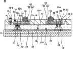
With reference to Figure 11, comprise according to the semiconductor device 10 of first embodiment: semiconductor chip 11, inner splicing ear 12, resin component 13, Wiring pattern 14, conducting terminal 16, solder mask 17 and external connection terminals 18.
Semiconductor integrated circuit 22 is arranged on the surperficial 21A side of semiconductor substrate 21.Semiconductor integrated circuit 22 is by being formed on diffusion layer (not shown) on the semiconductor substrate 21, being layered in the insulating barrier (not shown) on the semiconductor substrate 21 and being arranged on the stacked insulating barrier and the Wiring pattern (not shown) that is electrically connected with the diffusion layer (not shown) is formed.
A plurality of electrode pads 23 are arranged on the semiconductor integrated circuit 22.Electrode pad 23 is electrically connected with Wiring pattern (not shown) on being arranged on semiconductor integrated circuit 22.For example, can use the material of aluminum or aluminum alloy (for example, Al-Si-Cu alloy) as electrode pad 23.
For example, can use metal film that nickel film that forms by au bump, gold-plated film, by the plated by electroless plating method and the golden film that covers the nickel film form as inner splicing ear 12.Using under the situation of au bump as inner splicing ear 12, can form inner splicing ear 12 by for example combined techniques or galvanoplastic.
Figure 12 is the plane graph that is used for illustrating the resin component that is arranged on semiconductor device shown in Figure 11.In Figure 12, has identical Reference numeral with the element components identical of semiconductor device 10 shown in Figure 11.
With reference to Figure 11 and Figure 12, resin component 13 has resin component main body 13-1 and ledge 13-2.Resin component main body 13-1 is used to cover the upper surface of the part that inner splicing ear 12 is not set of side surface, electrode pad 23 of inner splicing ear 12 and the upper surface of diaphragm 24.See that in the plane resin component main body 13-1 is square.The upper surface 13-1A of resin component main body 13-1 almost is flat.The upper surface 12A of the upper surface 13-1A of resin component main body 13-1 and inner splicing ear 12 upper ends is almost contour.Wiring pattern 14 is formed on the upper surface 13-1A of resin component main body 13-1.The thickness M that is arranged in the part between solder mask 17 and the diaphragm 24 of resin component main body 13-1
1Can be set to for example 30 μ m to 50 μ m.
Ledge 13-2 is cylindrical and be arranged on the upper surface 13-1A of resin component main body 13-1.Ledge 13-2 one by one is arranged near four angle parts of resin component main body 13-1.Ledge 13-2 makes the etchant resist exposure so that be used as the parts of alignment mark in the processing of Wiring pattern 14 patternings, and wherein Wiring pattern 14 will be described below.The diameter R of ledge 13-2
1Can be set to for example 100 μ m.In addition, the height H of ledge 13-2
2Can be set to for example 50 μ m.For example, can use bottom potting resin or moulded resin (for example, epoxy resin) as resin component 13 with this structure.
Ledge 13-2 is arranged on the upper surface 13-1A that is formed with Wiring pattern 14 of resin component main body 13-1, therefore, so that when making the processing of metal level as Wiring pattern 14 base materials (being formed on the metal level on the upper surface 13-1A of resin component main body 13-1) patterning, can use ledge 13-2 when making etchant resist exposure as alignment mark.Therefore, compare, can improve the precision that etchant resist forms the position more significantly with routine techniques.Therefore, can improve the positional precision that forms Wiring pattern 14 with respect to inner splicing ear 12.
On the lower surface of the part relative that conducting terminal 16 is arranged on Wiring pattern 14 with inner splicing ear 12.Conducting terminal 16 is arranged to cover the side surface of inner splicing ear 12 upper ends.Conducting terminal 16 is used for inner splicing ear 12 is fixed on Wiring pattern 14.For example, can use conductive paste (more specifically being for example silver paste or copper cream) or salient point (more specifically being for example au bump or copper bump) as conducting terminal 16.
According to the semiconductor device of present embodiment, ledge 13-2 is arranged on the upper surface that is formed with Wiring pattern 14 of resin component main body 13-1.Therefore, so that when making the processing of metal level as Wiring pattern 14 base materials (being formed on the metal level on the upper surface 13-1A of resin component main body 13-1) patterning, can use ledge 13-2 when making etchant resist exposure as alignment mark.Therefore, compare, can improve the precision that etchant resist forms the position more significantly with routine techniques.Therefore, can improve the positional precision that forms Wiring pattern 14 with respect to inner splicing ear 12.
In addition, when being formed for making the etchant resist (not shown) of metal level as Wiring pattern 14 base materials (being formed on the metal level on the upper surface 13-1A of resin component main body 13-1) patterning, can use cheap exposure sources (not shown) to survey ledge 13-2 as alignment mark with CCD camera (not shown).Therefore, can reduce the manufacturing cost of semiconductor device 10.
In the present embodiment, though be described as example with the situation that four ledge 13-2 are set in the corner portions located that is foursquare resin component main body 13-1 from the plane, can this four ledge 13-2 be set in the regional corresponding part of resin component main body 13-1 with form the zone except that the Wiring pattern that is formed with Wiring pattern 14.In this case, can produce and the advantage identical according to the semiconductor device 10 of present embodiment.
In addition, in the present embodiment, though be described as example with the situation that four ledge 13-2 are set, it is just enough that at least two ledge 13-2 are set.In this case, can produce equally and the advantage identical according to the semiconductor device 10 of present embodiment.
Figure 13 to Figure 27 illustrates the view of manufacturing according to the step of the semiconductor device of first embodiment of the invention.Figure 28 is the plane graph that is used to illustrate having the penetrating component that forms on the supporter of metal level.In Figure 13 to Figure 28, has identical Reference numeral with element components identical according to the semiconductor device 10 of first embodiment.In addition, in Figure 18 to Figure 27, B represents to form the zone (following will being called " semiconductor device formation area B ") of semiconductor device 10, and C represents the position (following will calling " cutting position C ") of cutting semiconductor substrate 35 when semiconductor device 10 is divided into single.
With reference to figures 13 to Figure 28, will be described the method for manufacturing according to the semiconductor device of first embodiment.At first; in step shown in Figure 13; form on the semiconductor substrate 35 in zone and form a plurality of semiconductor chips 11 having a plurality of semiconductor chips, on electrode pad 23, form inner splicing ear 12 (inner splicing ear formation step) then with semiconductor integrated circuit 22, electrode pad 23 and diaphragm 24.In the step shown in Figure 27 that will describe hereinafter with semiconductor substrate 35 cutting and be divided into single, thereby as with reference to the described semiconductor substrate 21 of Figure 11.For example, can use silicon wafer as semiconductor substrate 35.The thickness of semiconductor substrate 35 can be set to for example 500 μ m to 700 μ m.Can use the material of aluminum or aluminum alloy (for example, Al-Si-Cu alloy) as electrode pad 23.For example, can use SiN film or psg film as diaphragm 24.
For example, can use metal film that nickel film that forms by au bump, gold-plated film, by the plated by electroless plating method and the golden film that covers the nickel film form as inner splicing ear 12.Using under the situation of au bump as inner splicing ear 12, can form inner splicing ear 12 by for example combined techniques or galvanoplastic.In this stage, the height of inner splicing ear 12 is different.In addition, in this stage, the upper surface of inner splicing ear 12 upper ends is not flat.
Subsequently, in step shown in Figure 14, preparation has the supporting bracket 37 of metal level, wherein sticks on the surperficial 38A last (preparation has the step of the supporting bracket of metal level) of supporting bracket 38 as the metal level 39 of Wiring pattern 14 base materials.Metal level 39 sticks on the supporting bracket 38, is in the state that can peel off from supporting bracket 38.As long as supporting bracket 38 is plate-shaped members that can support metal layer 39 and is separated just enough easily.More particularly, for example, can use metallic plate (for example, copper coin), metal forming (for example, Copper Foil) and resin plate as supporting bracket 38.Using under the situation of Copper Foil as supporting bracket 38, the thickness of supporting bracket 38 can be set to for example 35 μ m.For example, can use the copper layer as metal level 39.Using under the situation of copper layer as metal level 39, the thickness of metal level 39 can be set to for example 12 μ m.
Next, in step shown in Figure 15, in the part relative of supporting bracket 37, form penetrating component 41 (penetrating component formation step) with metal level with semiconductor chip shown in Figure 13 11.For example, as shown in figure 28, penetrating component 41 is formed in the part each supporting bracket 37, relative with four angle parts the external position A that is foursquare semiconductor chip 11 from the plane with metal level.For example, can be by forming penetrating component 41 such as digging methods such as carving processing, boring or punching press.In addition, can use cylindrical, positive cylindricality or otch shapes such as (grooves) shape (in Figure 15, cylindrical penetrating component 41 being shown) with way of example as penetrating component 41.Under penetrating component 41 cylindrical situations, the diameter R of penetrating component 41
2Can be set to for example 100 μ m.
Then, in step shown in Figure 16, on the relative part of inside splicing ear metal level 39 and that in structure shown in Figure 13, be provided with 12, form conducting terminal 16 (conducting terminal formation step).For example, can use conductive paste (more specifically being for example silver-colored conductive paste or copper conductive paste) or salient point (more specifically being for example au bump or copper bump) as conducting terminal 16.
Afterwards, in step shown in Figure 17, use is formed on penetrating component 41 on the supporting bracket 37 with metal level as alignment mark, the semiconductor chip 11 that is formed on the semiconductor substrate 35 is arranged to toward each other with the supporting bracket 37 with metal level, makes the inside splicing ear 12 that in structure shown in Figure 13, is provided with relative with the conducting terminal 16 that in structure as shown in figure 16, is provided with.
Subsequently, in step shown in Figure 180, under the state of heating inner splicing ear 12 and conducting terminal 16 (for example, using under the situation of au bump as conducting terminal 16, heating-up temperature is 180 °), push supporting bracket 37, make the upper end of inner splicing ear 12 contact, thereby make inner splicing ear 12 combine (Figure 17 and step shown in Figure 180 are represented the pressure integrating step) with metal level 39 pressure with metal level 39 with metal level.At this moment, the upper end of inner splicing ear 12 and metal level 39 contact with each other, and be mutually the same thereby height that can inner splicing ear 12 is set to, and the upper end face 12A of inner splicing ear 12 almost flattens.The height H of the inside splicing ear 12 that after the pressure integrating step, obtains
1Can be set to for example 30 μ m to 50 μ m.In addition, the gap between diaphragm 24 and the metal level 39 can be set to for example 30 μ m to 50 μ m.
Therefore, when when being formed on semiconductor chip 11 on the semiconductor substrate 35 and being arranged to toward each other with supporting bracket 37 with metal level, use is formed on penetrating component 41 on the supporting bracket 37 with metal level as alignment mark, aims at with can making conducting terminal 16 and inner splicing ear 12 pinpoint accuracy.Therefore, can strengthen inner splicing ear 12 and the reliability of electrical connection of metal level 39 (Wiring pattern 14) at the part place that is provided with conducting terminal 16.
In addition, under the state of inner splicing ear 12 of heating and conducting terminal 16, push supporting bracket 37 with metal level, so that inner splicing ear 12 combines with metal level 39 pressure, this can carry out the mutually the same step of the height that makes inner splicing ear 12 simultaneously and make inner splicing ear 12 and Wiring pattern 14 step of connecting, and these steps are separately finished in routine techniques.Therefore, can reduce the manufacturing cost of semiconductor device 10.
Subsequently, in step shown in Figure 19, the part and the penetrating component 41 that are formed on the semiconductor chip 11 on the semiconductor substrate 35 and have between the supporting bracket 37 of metal level are sealed (sealing step) with resin.Resin 46 is the base material of resin component shown in Figure 11 13 mentioned above.For example, can use bottom potting resin or moulded resin (for example, epoxy resin) as resin 46.
Using under the situation of moulded resin as resin 46, can form resin 46 by transmitting mechanography.As shown in figure 19, in this case, structure shown in Figure 180 is contained between lower mold 43 and the upper mold 44, then resin 46 is pressed into part between lower mold 43 and the upper mold 44.Therefore, seal with 46 pairs of semiconductor chips 11 of resin and the part and the penetrating component 41 that have between the supporting bracket 37 of metal level.
In addition,, preferably between upper mold 44 and supporting bracket 38, form the gap, make upper mold 44 not contact each other with supporter 38 using under the situation of transmitting mechanography formation resin 46.Therefore, between upper mold 44 and supporter 38, form the gap, make supporting bracket 37 can not be subjected to upper mold 44 and push with metal level.Therefore, can prevent metal level 14 bendings as Wiring pattern 14 base materials.In this case, resin 46 forms the upper surface that covers supporting bracket 38.In step shown in Figure 19, being that example is described by transmitting the situation that mechanography forms as the resin 46 of resin component 13 base materials.
Subsequently, in step shown in Figure 20, from being formed with the structure removal shown in Figure 180 lower mold 43 and the upper mold 44 as shown in figure 19 of resin 46.
Subsequently, in step shown in Figure 21, peel off supporting bracket 38, and the resin 46 that is formed on the supporting bracket 38 is removed with supporting bracket 38, thereby forms ledge 13-2 (ledge formation step) from the metal level 39 that structure shown in Figure 20, is provided with.Therefore, formed the resin component 13 that comprises resin component main body 13-1 and ledge 13-2.
The thickness M of resin component main body 13-1
1(thickness that is arranged in the part between diaphragm 24 and the metal level 39 of resin component main body 13-1) for example can be set to 30 μ m to 50 μ m.Ledge 13-2 one by one is formed near four angle parts of resin component main body 13-1.Under the situation of the cylindrical shape of ledge 13-2, the diameter R of ledge 13-2
1Can be set to for example 100 μ m.The height H of ledge 13-2
2Can be set to for example 50 μ m.In addition, the overhang E from metal level 39 upper surface 39A of ledge 13-2 can be set to for example 38 μ m.
Subsequently, in step shown in Figure 22, use ledge 13-2 as alignment mark so that form etchant resist 48, this etchant resist cover metal level 39 with the regional corresponding part (etchant resist formation step) that forms Wiring pattern 14.Etchant resist 48 is as the mask of etch metal layers 39.More particularly, at etchant resist 48 is under the situation of positive etchant resist, resist is applied on the metal level 39, use the position of cheap exposure sources (not shown) detection then as the ledge 13-2 of alignment mark with CCD camera (not shown), and rayed this resist with the regional corresponding part that forms Wiring pattern 14 on to carry out exposure-processed, after this resist that again back of exposing is obtained carries out development treatment, thereby has formed etchant resist 48.
Therefore, when being carried out exposure-processed, etchant resist 48,, can improve the positional precision of formation etchant resist 48 more significantly than routine techniques by using ledge 13-2 as alignment mark so that when making metal level 39 patternings as Wiring pattern 14 base materials.Therefore, can improve the positional precision that forms Wiring pattern 14 with respect to inner splicing ear 12.
In addition, so that when making metal level 39 patternings as Wiring pattern 14 base materials, can use cheap exposure sources (not shown) to survey position when forming as the ledge 13-2 of alignment mark with CCD camera (not shown) as the etchant resist (not shown) of mask.Therefore, can reduce the manufacturing cost of semiconductor device 10.
Next, in step shown in Figure 23, by using etchant resist 48 metal level 39 shown in Figure 22 to be carried out etching (more specifically being for example anisotropic etching), so that form the Wiring pattern 14 (Wiring pattern formation step) that is connected with inner splicing ear 12 as mask.In Figure 21 to Figure 23, be that example is described with the situation that forms Wiring pattern 14 by subtractive process.
Next, in step shown in Figure 25, on the upper surface 13-1A of resin component main body 13-1, form solder mask 17 by known technology, this solder mask covers the part except that pad portion 27 and the ledge 13-2 of Wiring pattern 14, forms external connection terminals 18 then on pad portion 27.Solder mask 17 has the opening portion 29 that pad portion of making 27 is exposed.For example, can use solder bump as external connection terminals 18.
Subsequently, in step shown in Figure 26, reduce the thickness of semiconductor substrate 35 from the back side 35B side of semiconductor substrate 35 shown in Figure 25.More particularly, from the back side 35B side of semiconductor substrate 35 semiconductor substrate 35 is polished or grinds, thereby semiconductor substrate 35 is become thin plate.Therefore, form at the semiconductor device of semiconductor substrate 35 and form the structure corresponding in the area B with semiconductor device 10.In order to reduce the thickness of semiconductor substrate 35, can use for example grinding back surface machine.The thickness of the semiconductor substrate 35 that obtains after reducing thickness can be set to for example 100 μ m to 300 μ m.
Next, in step shown in Figure 27, to cutting with the corresponding part of cutting position C of structure shown in Figure 26.Therefore, this structure is divided into single, thereby has made semiconductor device 10.
Method according to the semiconductor device of making present embodiment, under the state of inner splicing ear 12 of heating and conducting terminal 16, push supporting bracket 37 so that inner splicing ear 12 combines with metal level 39 pressure with metal level, this can carry out the mutually the same step of the height that makes inner splicing ear 12 simultaneously and make inner splicing ear 12 and Wiring pattern 14 step of connecting, and these steps are separately finished in routine techniques.Therefore, can reduce the manufacturing cost of semiconductor device 10.
In addition, when to carrying out exposure-processed as the etchant resist 48 of mask so that when making metal level 39 patternings as Wiring pattern 14 base materials, use ledge 13-2 as alignment mark, this can improve the positional precision that forms etchant resist 48 more significantly than routine techniques.Therefore, can improve the positional precision that forms Wiring pattern 14 with respect to inner splicing ear 12.
In addition, so that when making metal level 39 patternings as Wiring pattern 14 base materials, can use cheap exposure sources (not shown) to survey position when forming as the ledge 13-2 of alignment mark with CCD camera (not shown) as the etchant resist 48 of mask.Therefore, can reduce the manufacturing cost of semiconductor device 10.
(second embodiment)
Figure 29 is the cutaway view that illustrates according to the semiconductor device of second embodiment of the invention.In Figure 29, has identical Reference numeral with element components identical according to the semiconductor device 10 of first embodiment.
With reference to Figure 29, replace being arranged in according to the Wiring pattern 14 in the semiconductor device 10 of first embodiment (by the Wiring pattern that uses subtractive process to form) except Wiring pattern 51 is set, have the structure identical with the structure of semiconductor device 10 according to the semiconductor device 50 of second embodiment.
Electroplating film 55 is layered on the metal level 54.For example, can use copper plating film as electroplating film 55.Using under the situation of copper plating film as electroplating film 55, the thickness of electroplating film 55 can be set to for example 10 μ m.Can form electroplating film 55 by for example electrolysis.Can form Wiring pattern 51 by for example semi-additive process with this structure.
Can produce and the advantage identical according to the semiconductor device with this structure 50 of second embodiment according to the semiconductor device 10 of first embodiment.
Figure 30 to Figure 37 illustrates the view of manufacturing according to the step of the semiconductor device of second embodiment of the invention.In Figure 30 to Figure 37, has identical Reference numeral with element components identical according to the semiconductor device 50 of second embodiment.
With reference to Figure 30 to Figure 37, will be described the method for manufacturing according to the semiconductor device 50 of second embodiment.At first; carry out and step that describe in first embodiment and that step shown in Figure 13 is identical; to form on the semiconductor substrate 35 in zone and form a plurality of semiconductor chips 11 having a plurality of semiconductor chips, on electrode pad 23, form inner splicing ear 12 (inner splicing ear formation step) then with semiconductor integrated circuit 22, electrode pad 23 and diaphragm 24.
Subsequently, in step shown in Figure 30, preparation has the supporting bracket 57 of metal level, wherein sticks on the surperficial 38A last (preparation has the step of the supporting bracket of metal level) of supporting bracket 38 as the metal level 54 of the feed layer that forms electroplating film 55 (seeing Figure 29).Metal level 54 sticks on the supporting bracket 38, is in the state that can peel off from supporting bracket 38.Supporting bracket 38 is can support metal layer 54 just enough.More particularly, for example, can use metallic plate (for example, copper coin), metal forming (for example, Copper Foil) and resin plate as supporting bracket 38.Using under the situation of Copper Foil as supporting bracket 38, the thickness of supporting bracket 38 can be set to for example 35 μ m.For example, can use the copper layer as metal level 54.Using under the situation of copper layer as metal level 54, the thickness of metal level 54 can be set to for example 2 μ m to 3 μ m.
Next, in step shown in Figure 31, in the part relative of supporting bracket 57, form penetrating component 41 (penetrating component formation step), this semiconductor chip 11 has been shown among the Figure 13 that describes in first embodiment with metal level with semiconductor chip 11.For example, penetrating component 41 one by one is formed in part supporting bracket 37, relative with four angle parts among the external position A that is foursquare semiconductor chip 11 from the plane with metal level.For example, can be by forming penetrating component 41 such as digging methods such as carving processing, boring or punching press.In addition, can use cylindrical, square column type or otch (groove) shape as penetrating component 41.Under penetrating component 41 cylindrical situations, the diameter R of penetrating component 41
2Can be set to for example 100 μ m.
Then, in step shown in Figure 32, in the part relative of metal level 54, form conducting terminal 16 (conducting terminal formation step), inner splicing ear 12 has been shown among the Figure 13 that describes in first embodiment with inner splicing ear 12.For example, can use conductive paste (more specifically being for example silver-colored conductive paste or copper conductive paste) or salient point (more specifically being for example au bump or copper bump) as conducting terminal 16.
Afterwards, in step shown in Figure 33, carry out and the identical processing of the step shown in the Figure 17 to Figure 21 that in first embodiment, describes (comprising: pressure integrating step, sealing step and ledge form step), so that form structure shown in Figure 33.The height H of the inside splicing ear 12 that after the pressure integrating step, obtains
1Can be set to for example 30 μ m to 50 μ m.In addition, the gap between diaphragm 24 and the metal level 39 can be set to for example 30 μ m to 50 μ m.The thickness M of resin component main body 13-1
1Can be set to for example 30 μ m to 50 μ m.Ledge 13-2 one by one is arranged near four angle parts of resin component main body 13-1.Under the cylindrical situation of ledge 13-2, the diameter R of ledge 13-2
1Can be set to for example 100 μ m.The height H of ledge 13-2
2Can be set to for example 50 μ m.In addition, ledge 13-2 can be set to for example 48 μ m from the outstanding overhang E of the upper surface 39A of metal level 39.
Subsequently, in step shown in Figure 34, use ledge 13-2 as alignment mark, so that on resin component 13 and metal level 54, form etchant resist 61 with opening portion 61A, wherein opening portion is positioned at and the zone that forms Wiring pattern 51 (more particularly, formation is as the zone of the electroplating film 55 of one of Wiring pattern 51 elements) corresponding part (etchant resist formation step).More particularly, at etchant resist 61 is under the situation of positive etchant resist, form etchant resist 61 in the following manner: resist is applied on the metal level 54 with opening portion 61A, use the position of cheap exposure sources (not shown) detection then as the ledge 13-2 of alignment mark with CCD camera (not shown), and rayed this resist with the regional corresponding part that forms Wiring pattern 51 on to carry out exposure-processed, after this resist that again back of exposing is obtained carries out development treatment, thereby has formed etchant resist 61.Etchant resist 61 be only be used for metal level 54 with the regional corresponding part that forms Wiring pattern 51 on form the mask of electroplating film 55.
Therefore, when etchant resist 61 is carried out exposure-processed so that when making metal level 54 patternings as Wiring pattern 51 base materials, by using ledge 13-2 as alignment mark, can improve the positional precision of the opening portion 61A that forms etchant resist 61, wherein opening portion be formed on etchant resist with the corresponding part in the zone that forms Wiring pattern 51 (more particularly, form as the electroplating film 55 of one of Wiring pattern 51 elements zone).Therefore, can improve the positional precision that forms Wiring pattern 51 with respect to inner splicing ear 12.
In addition, so that when making metal level 54 patternings as Wiring pattern 51 base materials, can use cheap exposure sources (not shown) to survey position when forming as the ledge 13-2 of alignment mark with CCD camera (not shown) as the etchant resist 61 of mask.Therefore, can reduce the manufacturing cost of semiconductor device 50.
Subsequently, in step shown in Figure 35, by using the electrolytic plating method of metal level 54, form electroplating film 55 (electroplating film formation step) in the part of exposing from opening portion 61A of metal level 54 as feed layer.For example can use copper plating film as electroplating film 55.Using under the situation of copper plating film as electroplating film 55, the thickness of electroplating film 55 can be set to for example 10 μ m.
Next, in step shown in Figure 36, remove etchant resist 61 shown in Figure 35 (etchant resist removal step).Subsequently, in step shown in Figure 37, remove the part that does not form electroplating film 55 of metal level 54, formed the Wiring pattern of forming by metal level 54 and electroplating film 55 51 (Wiring pattern forms step).
Afterwards, carry out and the identical processing of step shown in the Figure 25 to Figure 27 that in first embodiment, describes, so that form semiconductor device 50.
According to the method for making the present embodiment semiconductor device, use ledge 13-2 to come etchant resist 61 is carried out exposure-processed, so that make metal level 54 patternings as Wiring pattern 51 base materials as alignment mark.Therefore, can improve the positional precision of the opening portion 61A that forms etchant resist 61, wherein opening portion be formed on etchant resist with the corresponding part in the zone that forms Wiring pattern 51 (more particularly, form as the electroplating film 55 of one of Wiring pattern 51 elements zone).Therefore, can improve the positional precision that forms Wiring pattern 51 with respect to inner splicing ear 12.
In addition, so that when making metal level 54 patternings as Wiring pattern 51 base materials, can use cheap exposure sources (not shown) to survey position when forming as the ledge 13-2 of alignment mark with CCD camera (not shown) as the etchant resist 61 of mask.Therefore, can reduce the manufacturing cost of semiconductor device 50.
Though described in detail according to a preferred embodiment of the invention, the invention is not restricted to these specific embodiments, but can under not breaking away from, carry out variations and modifications as the situation of the described scope of the invention of claims.
The present invention can be applied to make the method for the semiconductor device that comprises semiconductor chip, and wherein this semiconductor device comprises: electrode pad, the Wiring pattern that is arranged on the inside splicing ear on the electrode pad and is electrically connected with inner splicing ear.
Claims (10)
1. method of making semiconductor device, described semiconductor device comprises: a plurality of semiconductor chips, it comprises electrode pad; Semiconductor substrate, it has a plurality of semiconductor chips and forms the zone, and described semiconductor chip forms in the zone at described semiconductor chip and forms; Inner splicing ear, it is arranged on the described electrode pad; And Wiring pattern, it is electrically connected with described inner splicing ear,
Said method comprising the steps of:
On the electrode pad of described semiconductor chip, form described inner splicing ear;
Preparation has the supporting bracket of metal level, and wherein the metal level as the Wiring pattern base material is arranged on the supporting bracket;
In the part relative of described supporting bracket with metal level, form penetrating component with described semiconductor chip;
On the part relative of described metal level, form conducting terminal with described inner splicing ear;
Described semiconductor chip and described supporting bracket with metal level are arranged to toward each other, make described inner splicing ear and described conducting terminal toward each other, push described supporting bracket then, described inner splicing ear is combined with described metal level pressure with metal level;
After the pressure integrating step, with resin-sealed part and described penetrating component between described semiconductor chip and described supporting bracket with metal level;
After the sealing step, remove described supporting bracket, and on the part relative described resin, form ledge with penetrating component described supporting bracket;
Use described ledge as alignment mark, form and cover etchant resist described metal level and the regional corresponding part formation Wiring pattern; And
Use described etchant resist described metal level to be carried out etching, thereby form Wiring pattern as mask.
2. the method for manufacturing semiconductor device according to claim 1,
Wherein, in the step of described formation penetrating component, form at least two penetrating components.
3. the method for manufacturing semiconductor device according to claim 1,
Wherein, in the step of described formation penetrating component, the described penetrating component of formation in regional corresponding part described supporting bracket with metal level and except the zone that forms Wiring pattern.
4. the method for manufacturing semiconductor device according to claim 1,
Wherein, in described pressure integrating step, use the described penetrating component be formed on the described supporting bracket with metal level, described semiconductor chip and described supporting bracket with metal level are arranged to toward each other as alignment mark.
5. the method for manufacturing semiconductor device according to claim 1,
Wherein, in described sealing step, form described resin by transmitting mechanography.
6. method of making semiconductor device, described semiconductor device comprises: a plurality of semiconductor chips, it comprises electrode pad; Semiconductor substrate, it has a plurality of semiconductor chips and forms the zone, and described semiconductor chip forms in the zone at described semiconductor chip and forms; Inner splicing ear, it is arranged on the described electrode pad; And Wiring pattern, it is electrically connected with described inner splicing ear,
Said method comprising the steps of:
On the electrode pad of described semiconductor chip, form described inner splicing ear;
Preparation has the supporting bracket of metal level, and wherein metal level is arranged on the supporting bracket;
In the part relative of described supporting bracket with metal level, form penetrating component with described semiconductor chip;
On the part relative of described metal level, form conducting terminal with described inner splicing ear;
Described semiconductor chip and described supporting bracket with metal level are arranged to toward each other, make described inner splicing ear and described conducting terminal toward each other, push described supporting bracket then, described inner splicing ear is combined with described metal level pressure with metal level;
After the pressure integrating step, with resin-sealed part and described penetrating component between described semiconductor chip and described supporting bracket with metal level;
After the sealing step, remove described supporting bracket, and on the part relative described resin, form ledge with penetrating component described supporting bracket;
Use described ledge on described metal level, to form etchant resist with opening portion as alignment mark, described opening portion be arranged in described etchant resist with the regional corresponding part that forms Wiring pattern;
By using the electrolytic plating method of described metal level, form electroplating film in the part of exposing from opening portion of described metal level as feed layer;
After the step that forms electroplating film, remove described etchant resist; And
Remove the top part that does not form electroplating film of described metal level, so that form the Wiring pattern of forming by metal level and electroplating film.
7. the method for manufacturing semiconductor device according to claim 6,
Wherein, in the step of described formation penetrating component, form at least two penetrating components.
8. the method for manufacturing semiconductor device according to claim 6,
Wherein, in the step of described formation penetrating component, the described penetrating component of formation in regional corresponding part described supporting bracket with metal level and except the zone that forms Wiring pattern.
9. the method for manufacturing semiconductor device according to claim 6,
Wherein, in described pressure integrating step, use the described penetrating component be formed in the described supporting bracket with metal level, described semiconductor chip and described supporting bracket with metal level are arranged to toward each other as alignment mark.
10. the method for manufacturing semiconductor device according to claim 6,
Wherein, in described sealing step, form described resin by transmitting mechanography.
Applications Claiming Priority (2)
| Application Number | Priority Date | Filing Date | Title |
|---|---|---|---|
| JP2007241375A JP5064158B2 (en) | 2007-09-18 | 2007-09-18 | Semiconductor device and manufacturing method thereof |
| JP2007241375 | 2007-09-18 |
Publications (1)
| Publication Number | Publication Date |
|---|---|
| CN101393877A true CN101393877A (en) | 2009-03-25 |
Family
ID=40227776
Family Applications (1)
| Application Number | Title | Priority Date | Filing Date |
|---|---|---|---|
| CNA2008101612052A Pending CN101393877A (en) | 2007-09-18 | 2008-09-18 | Method of manufacturing a semiconductor device |
Country Status (6)
| Country | Link |
|---|---|
| US (1) | US7615408B2 (en) |
| EP (1) | EP2040294B1 (en) |
| JP (1) | JP5064158B2 (en) |
| KR (1) | KR20090029646A (en) |
| CN (1) | CN101393877A (en) |
| TW (1) | TW200917365A (en) |
Cited By (2)
| Publication number | Priority date | Publication date | Assignee | Title |
|---|---|---|---|---|
| CN102280426A (en) * | 2010-06-11 | 2011-12-14 | 卡西欧计算机株式会社 | Semiconductor device and manufacturing method of the same |
| CN103205701A (en) * | 2012-01-16 | 2013-07-17 | 昆山允升吉光电科技有限公司 | A vapor deposition mask plate and a production method thereof |
Families Citing this family (5)
| Publication number | Priority date | Publication date | Assignee | Title |
|---|---|---|---|---|
| JP5126370B2 (en) * | 2008-12-16 | 2013-01-23 | 株式会社村田製作所 | Circuit module |
| JP5160498B2 (en) * | 2009-05-20 | 2013-03-13 | ルネサスエレクトロニクス株式会社 | Semiconductor device |
| US9235674B2 (en) | 2013-03-05 | 2016-01-12 | Oracle International Corporation | Mitigating electromigration effects using parallel pillars |
| US10551165B2 (en) * | 2015-05-01 | 2020-02-04 | Adarza Biosystems, Inc. | Methods and devices for the high-volume production of silicon chips with uniform anti-reflective coatings |
| US11056410B2 (en) * | 2017-03-31 | 2021-07-06 | National Institute Of Advanced Industrial Science And Technology | Method of manufacturing semiconductor package using alignment mark on wafer |
Family Cites Families (14)
| Publication number | Priority date | Publication date | Assignee | Title |
|---|---|---|---|---|
| EP0734059B1 (en) * | 1995-03-24 | 2005-11-09 | Shinko Electric Industries Co., Ltd. | Chip sized semiconductor device and a process for making it |
| JP2843315B1 (en) * | 1997-07-11 | 1999-01-06 | 株式会社日立製作所 | Semiconductor device and manufacturing method thereof |
| US20040061220A1 (en) * | 1996-03-22 | 2004-04-01 | Chuichi Miyazaki | Semiconductor device and manufacturing method thereof |
| JPH10256306A (en) | 1997-03-12 | 1998-09-25 | Hitachi Chem Co Ltd | Preparation of circuit board |
| US20030001286A1 (en) * | 2000-01-28 | 2003-01-02 | Ryoichi Kajiwara | Semiconductor package and flip chip bonding method therein |
| JP3732378B2 (en) * | 2000-03-03 | 2006-01-05 | 新光電気工業株式会社 | Manufacturing method of semiconductor device |
| JP3638250B2 (en) * | 2000-10-11 | 2005-04-13 | シャープ株式会社 | Alignment mark and method for manufacturing semiconductor device |
| JP3614828B2 (en) * | 2002-04-05 | 2005-01-26 | 沖電気工業株式会社 | Manufacturing method of chip size package |
| JP2004193497A (en) * | 2002-12-13 | 2004-07-08 | Nec Electronics Corp | Chip-size package and manufacturing method thereof |
| TWI221330B (en) * | 2003-08-28 | 2004-09-21 | Phoenix Prec Technology Corp | Method for fabricating thermally enhanced semiconductor device |
| US8067823B2 (en) * | 2004-11-15 | 2011-11-29 | Stats Chippac, Ltd. | Chip scale package having flip chip interconnect on die paddle |
| JP2006013533A (en) * | 2005-07-28 | 2006-01-12 | Oki Electric Ind Co Ltd | Semiconductor device |
| JP2008108849A (en) | 2006-10-24 | 2008-05-08 | Shinko Electric Ind Co Ltd | Semiconductor device, and manufacturing method of semiconductor device |
| JP2008235555A (en) * | 2007-03-20 | 2008-10-02 | Shinko Electric Ind Co Ltd | Manufacturing method of electronic device, substrate, and semiconductor device |
-
2007
- 2007-09-18 JP JP2007241375A patent/JP5064158B2/en not_active Expired - Fee Related
-
2008
- 2008-09-11 KR KR1020080089605A patent/KR20090029646A/en not_active Application Discontinuation
- 2008-09-17 US US12/212,171 patent/US7615408B2/en active Active
- 2008-09-17 TW TW097135581A patent/TW200917365A/en unknown
- 2008-09-18 CN CNA2008101612052A patent/CN101393877A/en active Pending
- 2008-09-18 EP EP08164619.2A patent/EP2040294B1/en not_active Expired - Fee Related
Cited By (2)
| Publication number | Priority date | Publication date | Assignee | Title |
|---|---|---|---|---|
| CN102280426A (en) * | 2010-06-11 | 2011-12-14 | 卡西欧计算机株式会社 | Semiconductor device and manufacturing method of the same |
| CN103205701A (en) * | 2012-01-16 | 2013-07-17 | 昆山允升吉光电科技有限公司 | A vapor deposition mask plate and a production method thereof |
Also Published As
| Publication number | Publication date |
|---|---|
| KR20090029646A (en) | 2009-03-23 |
| JP2009076497A (en) | 2009-04-09 |
| EP2040294A1 (en) | 2009-03-25 |
| JP5064158B2 (en) | 2012-10-31 |
| TW200917365A (en) | 2009-04-16 |
| EP2040294B1 (en) | 2013-11-06 |
| US20090075422A1 (en) | 2009-03-19 |
| US7615408B2 (en) | 2009-11-10 |
Similar Documents
| Publication | Publication Date | Title |
|---|---|---|
| US7312521B2 (en) | Semiconductor device with holding member | |
| KR100475619B1 (en) | Wiring board, semiconductor device, and method of manufacturing wiring board | |
| US8344492B2 (en) | Semiconductor device and method of manufacturing the same, and electronic apparatus | |
| US8046912B2 (en) | Method of making a connection component with posts and pads | |
| KR101614960B1 (en) | Chip scale stacked die package | |
| KR100917745B1 (en) | Semiconductor device and manufacturing method thereof | |
| EP1662564A1 (en) | Semiconductor package and manufacturing method thereof | |
| CN101154606B (en) | Manufacturing method of semiconductor device | |
| US20040027477A1 (en) | Camera module and method for manufacturing the same | |
| US20040136123A1 (en) | Circuit devices and method for manufacturing the same | |
| CN101393877A (en) | Method of manufacturing a semiconductor device | |
| KR20090029660A (en) | Manufacturing method of semiconductor apparatus | |
| US6603210B2 (en) | Semiconductor module and producing method therefor | |
| KR20190015097A (en) | Chip Package and Method of Manufacturing the Same | |
| KR100611291B1 (en) | Circuit device, circuit module, and manufacturing method of the circuit device | |
| EP1478021B1 (en) | Semiconductor device and manufacturing method thereof | |
| US7443043B2 (en) | Circuit device and method of manufacture thereof | |
| JP4215571B2 (en) | Manufacturing method of semiconductor device | |
| JP5238985B2 (en) | Manufacturing method of semiconductor device | |
| JP4286264B2 (en) | Semiconductor device and manufacturing method thereof | |
| CN108962868B (en) | Package structure and method for fabricating the same | |
| US20040232566A1 (en) | Semiconductor device and method of manufacturing the same | |
| JP2006165109A (en) | Semiconductor device and its manufacturing method | |
| JP2021022591A (en) | Method for manufacturing semiconductor device and semiconductor device | |
| JP2006173376A (en) | Semiconductor apparatus and method for manufacturing the same |
Legal Events
| Date | Code | Title | Description |
|---|---|---|---|
| C06 | Publication | ||
| PB01 | Publication | ||
| C02 | Deemed withdrawal of patent application after publication (patent law 2001) | ||
| WD01 | Invention patent application deemed withdrawn after publication |
Open date: 20090325 |