EP2034523A1 - Nitride semiconductor light-emitting device - Google Patents
Nitride semiconductor light-emitting device Download PDFInfo
- Publication number
- EP2034523A1 EP2034523A1 EP06746880A EP06746880A EP2034523A1 EP 2034523 A1 EP2034523 A1 EP 2034523A1 EP 06746880 A EP06746880 A EP 06746880A EP 06746880 A EP06746880 A EP 06746880A EP 2034523 A1 EP2034523 A1 EP 2034523A1
- Authority
- EP
- European Patent Office
- Prior art keywords
- layer
- nitride semiconductor
- type
- undoped ingan
- light emitting
- Prior art date
- Legal status (The legal status is an assumption and is not a legal conclusion. Google has not performed a legal analysis and makes no representation as to the accuracy of the status listed.)
- Withdrawn
Links
- 239000004065 semiconductor Substances 0.000 title claims abstract description 106
- 150000004767 nitrides Chemical class 0.000 title claims abstract description 92
- 239000000203 mixture Substances 0.000 claims description 79
- 230000015572 biosynthetic process Effects 0.000 claims description 20
- 230000007423 decrease Effects 0.000 claims description 9
- 238000000034 method Methods 0.000 claims description 8
- 230000008569 process Effects 0.000 claims description 2
- 239000000758 substrate Substances 0.000 abstract description 21
- 238000002347 injection Methods 0.000 abstract description 15
- 239000007924 injection Substances 0.000 abstract description 15
- 229910052594 sapphire Inorganic materials 0.000 abstract description 11
- 239000010980 sapphire Substances 0.000 abstract description 11
- 238000005530 etching Methods 0.000 abstract description 6
- 229910002704 AlGaN Inorganic materials 0.000 description 27
- 238000010586 diagram Methods 0.000 description 21
- 238000005253 cladding Methods 0.000 description 20
- 235000019557 luminance Nutrition 0.000 description 19
- 230000004888 barrier function Effects 0.000 description 18
- IBEFSUTVZWZJEL-UHFFFAOYSA-N trimethylindium Chemical compound C[In](C)C IBEFSUTVZWZJEL-UHFFFAOYSA-N 0.000 description 15
- 238000005259 measurement Methods 0.000 description 14
- 238000005401 electroluminescence Methods 0.000 description 13
- 230000003247 decreasing effect Effects 0.000 description 9
- 238000000295 emission spectrum Methods 0.000 description 8
- 239000012535 impurity Substances 0.000 description 8
- 239000013078 crystal Substances 0.000 description 7
- 230000000694 effects Effects 0.000 description 6
- 238000005424 photoluminescence Methods 0.000 description 5
- VYPSYNLAJGMNEJ-UHFFFAOYSA-N silicon dioxide Inorganic materials O=[Si]=O VYPSYNLAJGMNEJ-UHFFFAOYSA-N 0.000 description 5
- VEXZGXHMUGYJMC-UHFFFAOYSA-N Hydrochloric acid Chemical compound Cl VEXZGXHMUGYJMC-UHFFFAOYSA-N 0.000 description 4
- MCMNRKCIXSYSNV-UHFFFAOYSA-N Zirconium dioxide Chemical compound O=[Zr]=O MCMNRKCIXSYSNV-UHFFFAOYSA-N 0.000 description 4
- 230000006872 improvement Effects 0.000 description 4
- 238000002488 metal-organic chemical vapour deposition Methods 0.000 description 4
- IJGRMHOSHXDMSA-UHFFFAOYSA-N Atomic nitrogen Chemical compound N#N IJGRMHOSHXDMSA-UHFFFAOYSA-N 0.000 description 3
- 230000008859 change Effects 0.000 description 3
- 238000009826 distribution Methods 0.000 description 3
- 238000004519 manufacturing process Methods 0.000 description 3
- 239000002184 metal Substances 0.000 description 3
- 238000004549 pulsed laser deposition Methods 0.000 description 3
- 229910004541 SiN Inorganic materials 0.000 description 2
- PNEYBMLMFCGWSK-UHFFFAOYSA-N aluminium oxide Inorganic materials [O-2].[O-2].[O-2].[Al+3].[Al+3] PNEYBMLMFCGWSK-UHFFFAOYSA-N 0.000 description 2
- 238000013459 approach Methods 0.000 description 2
- 229910052681 coesite Inorganic materials 0.000 description 2
- 150000001875 compounds Chemical class 0.000 description 2
- 229910052593 corundum Inorganic materials 0.000 description 2
- 229910052906 cristobalite Inorganic materials 0.000 description 2
- 239000002019 doping agent Substances 0.000 description 2
- 230000005284 excitation Effects 0.000 description 2
- 239000012212 insulator Substances 0.000 description 2
- 238000001451 molecular beam epitaxy Methods 0.000 description 2
- 238000007788 roughening Methods 0.000 description 2
- 239000000377 silicon dioxide Substances 0.000 description 2
- 229910052814 silicon oxide Inorganic materials 0.000 description 2
- 238000001228 spectrum Methods 0.000 description 2
- 229910052682 stishovite Inorganic materials 0.000 description 2
- 229910052905 tridymite Inorganic materials 0.000 description 2
- RGGPNXQUMRMPRA-UHFFFAOYSA-N triethylgallium Chemical compound CC[Ga](CC)CC RGGPNXQUMRMPRA-UHFFFAOYSA-N 0.000 description 2
- 229910001845 yogo sapphire Inorganic materials 0.000 description 2
- 230000004913 activation Effects 0.000 description 1
- 238000000137 annealing Methods 0.000 description 1
- 239000000969 carrier Substances 0.000 description 1
- 230000015556 catabolic process Effects 0.000 description 1
- 238000006243 chemical reaction Methods 0.000 description 1
- 238000004140 cleaning Methods 0.000 description 1
- 239000000470 constituent Substances 0.000 description 1
- 238000000354 decomposition reaction Methods 0.000 description 1
- 230000007547 defect Effects 0.000 description 1
- 238000006731 degradation reaction Methods 0.000 description 1
- 238000000151 deposition Methods 0.000 description 1
- 230000008021 deposition Effects 0.000 description 1
- 230000006866 deterioration Effects 0.000 description 1
- 238000001312 dry etching Methods 0.000 description 1
- 238000010438 heat treatment Methods 0.000 description 1
- 230000010354 integration Effects 0.000 description 1
- 238000000608 laser ablation Methods 0.000 description 1
- 239000000463 material Substances 0.000 description 1
- 229910052757 nitrogen Inorganic materials 0.000 description 1
- 230000003287 optical effect Effects 0.000 description 1
- 230000010355 oscillation Effects 0.000 description 1
- 239000010453 quartz Substances 0.000 description 1
- 230000006798 recombination Effects 0.000 description 1
- 238000005215 recombination Methods 0.000 description 1
- 238000003892 spreading Methods 0.000 description 1
- 230000007480 spreading Effects 0.000 description 1
- 238000004544 sputter deposition Methods 0.000 description 1
- 238000000859 sublimation Methods 0.000 description 1
- 230000008022 sublimation Effects 0.000 description 1
- 239000000126 substance Substances 0.000 description 1
- 238000001039 wet etching Methods 0.000 description 1
Images






Classifications
-
- H—ELECTRICITY
- H10—SEMICONDUCTOR DEVICES; ELECTRIC SOLID-STATE DEVICES NOT OTHERWISE PROVIDED FOR
- H10H—INORGANIC LIGHT-EMITTING SEMICONDUCTOR DEVICES HAVING POTENTIAL BARRIERS
- H10H20/00—Individual inorganic light-emitting semiconductor devices having potential barriers, e.g. light-emitting diodes [LED]
- H10H20/80—Constructional details
- H10H20/81—Bodies
- H10H20/822—Materials of the light-emitting regions
- H10H20/824—Materials of the light-emitting regions comprising only Group III-V materials, e.g. GaP
- H10H20/825—Materials of the light-emitting regions comprising only Group III-V materials, e.g. GaP containing nitrogen, e.g. GaN
-
- H—ELECTRICITY
- H10—SEMICONDUCTOR DEVICES; ELECTRIC SOLID-STATE DEVICES NOT OTHERWISE PROVIDED FOR
- H10H—INORGANIC LIGHT-EMITTING SEMICONDUCTOR DEVICES HAVING POTENTIAL BARRIERS
- H10H20/00—Individual inorganic light-emitting semiconductor devices having potential barriers, e.g. light-emitting diodes [LED]
- H10H20/80—Constructional details
- H10H20/81—Bodies
- H10H20/811—Bodies having quantum effect structures or superlattices, e.g. tunnel junctions
- H10H20/812—Bodies having quantum effect structures or superlattices, e.g. tunnel junctions within the light-emitting regions, e.g. having quantum confinement structures
-
- H—ELECTRICITY
- H10—SEMICONDUCTOR DEVICES; ELECTRIC SOLID-STATE DEVICES NOT OTHERWISE PROVIDED FOR
- H10H—INORGANIC LIGHT-EMITTING SEMICONDUCTOR DEVICES HAVING POTENTIAL BARRIERS
- H10H20/00—Individual inorganic light-emitting semiconductor devices having potential barriers, e.g. light-emitting diodes [LED]
- H10H20/80—Constructional details
- H10H20/81—Bodies
Definitions
- the present invention relates to a nitride semiconductor light emitting element including an active layer which has a quantum well structure with a well layer made of a nitride containing In.
- nitride semiconductors such as GaN, AlGaN, InGaN, InGaAlN and GaPN are used for short wavelength semiconductor lasers.
- LEDs using nitride semiconductors also have been developed.
- the nitride semiconductor light emitting elements As the nitride semiconductor light emitting elements, light emitting elements of the MIS structure have been used in some cases. However, such a light emitting element has a high-resistance i-type GaN-based semiconductor stacked thereon, and accordingly has a problem of generally very low emission output. To solve such a problem, the i-type GaN-based semiconductor layer is irradiated with electrons or is annealed.
- the forward voltage Vf be reduced by forming an ohmic contact between a p-electrode and a p-type GaN contact layer or by making smaller the film thickness of a p-type GaN contact layer.
- Patent Document 1 also proposes that Mg be used as a p-type dopant to obtain the p-type characteristics of a p-type AlGaN cladding layer, or that the film thickness and the Al composition of the p-type AlGaN cladding layer be specified to improve the crystallinity.
- the luminous efficiency is improved by the above prior art: by the improvements in the respective attributes of the ohmic contact between the p-electrode and the p-type GaN contact layer; the film thickness of the p-type GaN contact layer; the p-type dopant; and the crystallinity of the p-type AlGaN cladding layer, the effects from these improvements are limited. In addition, effective means for further increasing the luminous efficiency is not yet to be obtained.
- An object of the present invention is to provide a nitride semiconductor light emitting element having an improved carrier injection efficiency from a p-type nitride semiconductor layer to an active layer and an improved luminous efficiency by simple means from a viewpoint utterly different from the prior art.
- a nitride semiconductor light emitting element of the present invention is a nitride semiconductor light emitting element with a structure in which an active layer is sandwiched between a p-type nitride semiconductor layer and an n-type nitride semiconductor layer, the active layer having a quantum well structure with a well layer made of a nitride containing In.
- a first undoped InGaN layer and a second undoped InGaN layer with an In content different from that of the first undoped InGaN layer are formed between the p-type nitride semiconductor layer and the well layer of the active layer disposed at a position closest to a p-side, and that a total film thickness of the first undoped InGaN layer and the second undoped InGaN layer is 20 nm or less.
- the second undoped InGaN layer is an In composition gradient layer whose In content decreases toward the p-type nitride semiconductor layer.
- the hole carrier concentration is made to be in a range of 2 ⁇ 10 17 cm -3 or more.
- the other summary of the nitride semiconductor light emitting element of the present invention is that, when the well layer of the active layer has an In composition ratio of 10% or more and thus the emission wavelength becomes long, a total film formation time when a growth temperature exceeds 950°C is within 30 minutes from the time of completion of the formation of the final well layer of the active layer in a growth direction to the time of completion of the formation of a p-type contact layer that is formed as a part of the p-type nitride semiconductor layer, and that is in contact with a p-electrode.
- InGaN is thermally unstable and thus there arises a possibility of its decomposition when the above conditions are exceeded. In the worst case, the In is dissociated and the wafer is blackened.
- two undoped InGaN layers with different In contents from each other are formed between the p-type nitride semiconductor layer and the well layer of the active layer closest to the p-type side having the quantum well structure.
- the total film thickness of these two undoped InGaN layers is formed to be 20 nm or less.
- the undoped InGaN layer closer to the p-type nitride semiconductor layer is made to be an In composition gradient layer whose In content decreases toward the p-type nitride semiconductor layer. This makes it easy to inject holes into the active layer, thus improving the luminous efficiency.
- the p-type Al x GaN (0.02 ⁇ x ⁇ 0.15) is stacked on the two undoped InGaN layers and is formed such that the hole carrier concentration due to p-type impurities becomes 2x10 17 cm -3 or more. Thereby, the amount of holes injected into the active layer can be obtained sufficiently, and thus the luminous efficiency can be improved.
- the total film formation time when the growth temperature is 950°C or above is made to be within 30 minutes from the time of completion of the formation of the final well layer of the active layer in the growth direction to the time of the completion of the formation of the p-type contact layer that is formed as a part of the p-type nitride semiconductor layer, and that is in contact with the p-electrode.
- Fig. 1 shows a cross-sectional view of one example of a first nitride semiconductor light emitting element of the present invention.
- a buffer layer 2 On a sapphire substrate 1, stacked are a buffer layer 2, an undoped GaN layer 3, an n-type GaN contact layer 4, an InGaN/GaN superlattice layer 5, an active layer 6, a first undoped InGaN layer 7, a second undoped InGaN layer 8 and a p-type GaN-based contact layer 9.
- a region of the first nitride semiconductor light emitting element is partially mesa-etched from the p-type GaN-based contact layer 9, and an n-electrode 11 is formed on a surface where the n-type GaN contact layer 4 is exposed.
- a p-electrode 10 is formed on the p-type GaN-based contact layer 9.
- the p-type GaN-based layer is made up of GaN having doped therein p-type impurities or a compound including GaN.
- the undoped InGaN layer is made up of an InGaN layer in which no impurities are intentionally doped.
- the n-type GaN contact layer 4 and the InGaN/GaN superlattice layer 5 are formed as n-type nitride semiconductor layers.
- the p-type GaN-based contact layer 9 is formed as a p-type nitride semiconductor layer.
- the nitride semiconductor light emitting element of the present invention has a double heterostructure with these n-type nitride semiconductor layers and the p-type nitride semiconductor layer sandwiching the active layer.
- GaN, AlN, Al x1 GaN (0 ⁇ x1 ⁇ 0.1) or the like is used.
- the buffer layer 2 is formed in a film thickness of from 50 to 300 ⁇ , desirably from 100 to 200 ⁇ .
- the undoped GaN layer 3 stacked on the buffer layer 2 has a film thickness of 1 to 3 ⁇ m.
- the n-type GaN contact layer 4 formed on the undoped GaN layer 3 has a Si doping concentration of 1x10 18 cm -3 to 5x10 18 cm -3 and has a film thickness of 1 to 5 ⁇ m.
- the InGaN/GaN superlattice layer 5 relaxes the stress of InGaN and GaN that have a large difference in lattice constant from each other.
- the InGaN/GaN superlattice layer 5 causes the InGaN of the active layer 6 to grow readily.
- the InGaN/GaN superlattice layer 5 to be used has a constitution, for example, in which In x GaN (0.03 ⁇ x ⁇ 0.1) having a Si doping concentration of 1 ⁇ 10 18 cm -3 to 5 ⁇ 10 18 cm -3 and a film thickness of 10 ⁇ and GaN having a film thickness of 20 ⁇ are alternately stacked on each other at approximately 10 repetitions.
- the active layer 6 is an active layer that has a quantum well structure (Quantum Well) and has a structure in which a well layer is sandwiched with barrier layers each having a larger band-gap than the well layer.
- This quantum well structure may not only be a single structure, but be a multiplexed structure. In this multiplexed case, the structure becomes a MQW (Multi-Quantum Well), namely, a multiquantum well structure.
- the active layer 6 is made up of a ternary mixed crystal system of InGaN.
- the first undoped InGaN layer 7 is formed to contact the final well layer of the active layer 6 in a growth direction.
- the first undoped InGaN layer 7 has a role of a barrier layer or a cap layer of the active layer 6.
- Fig. 2 shows the structure of the active layer 6 in detail.
- a barrier layer 6b is disposed on a side of the InGaN/GaN superlattice layer 5 where the active layer 6 contacts the InGaN/GaN superlattice layer 5.
- a well layer 6c is stacked on the barrier layer 6b. This barrier layer 6b and the well layer 6c are alternately stacked on each other at a number of repetitions. Thereafter, the first undoped InGaN layer 7 is stacked on the final well layer 6c so as to be in contact with each other.
- the second undoped InGaN layer 8 is formed on the first undoped InGaN layer 7.
- the p-type Gan-based contact layer 9 is formed on the second undoped InGaN layer 8.
- the barrier layer 6b is made up of In z1 GaN (O ⁇ z1 ⁇ 1) either being non-doped or having an Si doping concentration of 5 ⁇ 10 16 cm -3 to 5 ⁇ 10 18 cm -3 and has a film thickness of 100 to 350 ⁇ , and desirably of 150 to 300 ⁇ .
- the well layer 6c may be made up of, for example, non-doped In y1 GaN (0 ⁇ y1 ⁇ 1, y1>z1) with a film thickness of 30 ⁇ .
- the Si doping concentration is desirably 5 ⁇ 10 18 cm -3 or less.
- 3 to 8 layers, desirably 5 to 7 layers, of the well layers are formed.
- the emission wavelength can be changed from purple to red by allowing the above y1 to be in a range of 0 ⁇ y1 ⁇ 1.
- the total film thickness of: the first undoped InGaN layer 7 formed to contact the final well layer of the active layer 6; and the second undoped InGaN layer 8 formed to contact the first undoped InGaN layer 7 is made to be 20 nm or less.
- the first undoped InGaN layer 7 has roles as an electron barrier layer that makes no electrons flow from the active layer 6 to the p-side and also as a cap layer of preventing the In of the well layer 6c from sublimating at high temperatures, the sublimating consequently causing the well layer 6c to readily break down.
- the first undoped InGaN layer 7 desirably has a band-gap energy equal to or more than that of the barrier layer 6b in order to have a band-gap energy larger than that of the well layer 6c and to thereby block electrons.
- This InGaN layer 7 is desired to be an InGaN layer with an In composition ratio of z1 or less.
- the second undoped InGaN layer 8 desirably has a band-gap energy larger than that of the first undoped InGaN layer 7 but smaller than that of the p-type Gan-based contact layer 9. Therefore, the In composition ratio of the second undoped InGaN layer 8 is desirably smaller than that of the first undoped InGaN layer 7 in a range excluding 0.
- P-type InGaN or p-type GaN is used for the p-type Gan-based contact layer 9 formed on the second undoped InGaN layer 8.
- This contact layer 9 has a Mg-doping concentration of 3 ⁇ 10 19 cm -3 to 3 ⁇ 10 20 cm -3 , and is grown to have a film thickness of approximately 200 to 3000 ⁇ (most desirably, 700 ⁇ to 1000 ⁇ ).
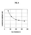
- Fig. 4 shows a manner in which the luminance changes according to the total film thickness of the first undoped InGaN layer 7 and the second undoped InGaN layer 8.
- the emission intensity (luminance) was measured by changing the total film thickness of the first undoped InGaN layer 7 and the second undoped InGaN layer 8 in constitution of Fig. 1 .
- the abscissa indicates the total film thickness of the two undoped InGaN layers.
- the ordinate indicates relative luminances based on the luminance at 250 ⁇ . When the total film thickness becomes 200 ⁇ (20 nm) or less, the luminance is shown to be greatly improved.
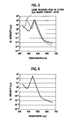
- Fig. 5 shows an emission spectrum when the total film thickness of the two undoped InGaN layers is 350 ⁇ in the constitution of Fig. 1 .
- the ordinate indicates relative luminances based on the emission intensity of a standard LED.
- Fig. 5 not only an original emission spectrum of the active layer 6 but also a spectrum of the undoped InGaN layer is also shown together.
- the recombination of a hole and an electron is generated not only in the active layer 6 but also in the undoped InGaN layers.
- the luminous efficiency of the active layer 6 decreases because holes are not sufficiently transferred from the p-type Gan-based contact layer 9 to the active layer 6.
- Fig. 6 shows an emission spectrum when the total film thickness of the undoped InGaN layers is 120 ⁇ . Only an original emission spectrum of the active layer 6 appears, but a spectrum of the undoped InGaN layer as in Fig. 5 does not appear. This is because, when the total film thickness of the undoped InGaN layers is smaller, the injection efficiency of holes from the p-type Gan-based contact layer 9 into the active layer 6 is improved. Therefore, the undoped InGaN layers with a smaller total film thickness lead to a larger emission intensity of the light emitting element. In addition, it can be recognized from Fig. 4 that the optimum value of this total film thickness is 200 ⁇ (20 nm) or less.
- Fig. 3 shows a constitution of a second nitride semiconductor light emitting element of the present invention.
- the constituents denoted by the same symbols as those in Fig. 1 are shown to have the same constitutions as those in Fig. 1 .
- the difference between the second nitride semiconductor light emitting element and the first nitride semiconductor light emitting element is that a p-type AlGan cladding layer 12 is inserted between the second undoped InGaN layer 8 and the p-type Gan-based contact layer 9.
- the p-type AlGan cladding layer 12 has a role of an electron barrier layer, and aims to further improve the injection efficiency of holes.
- p-type AlGan cladding layer 12 p-type Al x GaN (0.02 ⁇ x ⁇ 0.15) or the like is used.
- the carrier concentration of the p-type Al x GaN obtained by doping the impurity Mg therein is desirably in a range that is 2 ⁇ 10 17 cm -3 or more as described below.
- the p-type AlGan cladding layer 12 is made up of Al 0.07 GaN with a film thickness of 150 to 300 ⁇ (most desirably 200 ⁇ ).
- the luminance was measured by changing the total film thickness of the two undoped InGaN layers.
- the graphical form shown in Fig. 4 was obtained.
- Fig. 7 shows the relationship between the In composition ratio of the undoped InGaN layer and the luminance of the nitride semiconductor light emitting element.
- the abscissa shows the In composition ratio
- the ordinate shows the luminance (arbitrary unit).
- the ordinate indicates relative luminances based on the luminance measured when the In composition ratio is 0.5%.
- the luminances were measured in the constitutions of Figs. 1 and 3 .
- the In composition ratio of up to approximately 2.5% can be used for light-emission luminance. Meanwhile, as the ratio becomes more than 2.5%, the light-emission luminance considerably approaches 0, and the ratio of more than 2.5% is not usable.
- the In composition ratio is desirably 2.5% or less, most suitably in a range of 0.5% to 1%.
- Fig. 8 shows one example of the constitution of the first undoped InGaN layer 7 and the second undoped InGaN layer 8, with different In compositions from each other, using a band-gap energy diagram of conduction bands.
- the first undoped InGaN layer 7 plays a role as an electron barrier layer.
- This layer is configured to have a band-gap energy equal to or more than the band-gap energy of the barrier layer 6b.
- the second undoped InGaN layer 8 is configured to have a band-gap energy larger than that of the first undoped InGaN layer 7 but smaller than that of the p-type Gan-based contact layer 9.
- both the first undoped InGaN layer 7 and the second undoped InGaN layer 8 are formed so as to have an In composition ratio of 2.5% or less.
- the first and second undoped InGaN layers can be configured to have stepwise increased band-gaps in the order the first undoped InGaN layer 7, the second undoped InGaN layer 8 and the p-type nitride semiconductor layer, as shown in Fig. 8 .
- Fig. 9 shows a band-gap energy diagram of conduction bands in front and back of the active layer 6.
- the barrier layer 6b and the well layer 6c form a quantum well structure.
- the first undoped InGaN layer 7 is formed on the p-side to contact the final well layer 6c.
- the second undoped InGaN layer 8 is formed to contact this first undoped InGaN layer 7.
- the In composition ratio of this second undoped InGaN layer 8 decreases continuously from the junction with the first undoped InGaN layer 7 toward the direction of the p-type nitride semiconductor layer (rightward in the drawing).
- the decrease in the In composition ratio toward the p-type nitride semiconductor layer means that the band-gap energy of the second undoped InGaN layer 8 increases toward the p-type nitride semiconductor layer.
- the band structure in the conduction band that serves in hole conduction has a lower potential toward the well layer.
- the composition gradient of In is desirably fabricated at a high growth temperature.
- a PLD method laser ablation method
- the buffer layer 2 made of single crystals such as GaN, AlN and Al x1 GaN (0 ⁇ X1 ⁇ 0.1) on the sapphire substrate 1.
- the sapphire substrate 1 is placed in a load lock chamber and heated at a temperature of approximately 400°C for 5 to 10 minutes to remove excess moisture and the like. Thereafter, the sapphire substrate 1 is transported into a vacuum chamber with an internal pressure of 1 ⁇ 10 -6 Torr or less and is placed so as to oppose a target. The sapphire substrate 1 is placed on a heat source, and the substrate temperature is maintained at 600°C to 1000°C.
- the target is irradiated with the KrF excimer laser light having an oscillation wavelength of 248 nm from a quartz window of the vacuum chamber to thereby sublimate (ablate) the material of the target. This sublimated atom adheres to the surface of the sapphire substrate 1, and the buffer layer 2 of single crystal grows up.
- the buffer layer 2 forms into a thickness of, for example, 100 ⁇ to 200 ⁇ .
- a sintered GaN target is used as the target.
- a sintered body target of AlN, AlGaN, or InGaN may be used.
- a sintered body target of InGaN is a substance into which In is hardly incorporated in general. Therefore, a sintered body target of GaN, AlN or AlGaN is desired.
- the sapphire substrate 1 having the buffer layer 2 formed thereon as described above is placed in a load lock chamber of an MOCVD apparatus.
- This substrate is heated for 5 to 10 minutes at a temperature of approximately 400°C to remove excess moisture and the like, and then transported to a reaction chamber of the MOCVD apparatus.
- the substrate is subjected to thermal cleaning in the MOCVD apparatus at 1100°C for 30 minutes in an NH 3 atmosphere.
- the undoped GaN layer 3 is stacked.
- the substrate temperature is increased to 1065°C.
- undoped GaN is grown to 1 ⁇ m
- Si-doped n-type GaN is grown to 2.5 ⁇ m.
- the substrate temperature is lowered to 760 °C, and the InGaN/GaN superlattice layer 5 is formed to, for example, 300 ⁇ .
- the substrate temperature is lowered to 750°C, and the active layer 6 is formed to, for example, 3/17 nm.
- the first undoped InGaN layer 7 and the second undoped InGaN layer 8 are stacked thereon.
- the total film thickness of the first undoped InGaN layer 7 and the second undoped InGaN layer 8 is made to be 20 ⁇ m or less.
- the first undoped InGaN layer 7 and the second undoped InGaN layer 8 are film-formed to, for example, approximately 20 to 30 ⁇ .
- the second undoped InGaN layer 8 is not an In composition gradient layer, the In content of the first and second InGaN layers is made to be 2.5% or less, as can be recognized from Fig. 7 , but most suitably from approximately 0.5% to 1%.
- a p-type GaN layer is made to grow to, for example, 700 ⁇ as the p-type Gan-based contact layer 9 by increasing the growth temperature to 1000 to 1030°C (e.g., 1010°C).
- an Mg-doped p-type InGaN layer may be used. In this case also, this layer is made to grow to, for example, 700 ⁇ .
- a multi-level metal film such as Ti/Au is formed as the p-electrode 10 by deposition or sputtering.
- a mesa pattern is formed, and the GaN-based semiconductor laminated body is etched until the n-type GaN contact layer 4 is exposed therefrom.
- a sufficient etching depth is where the n-type GaN contact layer 4 is exposed.
- Fig. 1 After completion of the mesa etching, Al is formed on the n-type GaN contact layer 4 as the n-electrode 11, and is subjected to annealing at 500°C to 700°C to obtain an ohmic behavior. Thus, the constitution of Fig. 1 is completed.
- the p-electrode 10 is not formed on the p-type Gan-based contact layer 9, but the p-electrode 10 may be formed thereon after a ZnO electrode is stacked on the p-type Gan-based contact layer 9.
- a Ga-doped ZnO electrode is formed on the p-type Gan-based contact layer 9 by, for example, MBE (Molecular beam epitaxy) or PLD (Pulsed Laser Deposition).
- MBE Molecular beam epitaxy
- PLD Pulsed Laser Deposition
- Etching is performed till the p-type Gan-based contact layer 9 by use of wet etching with hydrochloric acid or dry etching such as RIE in order to make the ZnO electrode have predetermined dimensions. Thereafter, the entire ZnO is covered with an insulator such as SiN, SiON, SiO 2 , Al 2 O 3 or ZrO 2 .
- the mesa-etching is performed as described above, and the n-electrode 11 is formed on the n-type GaN contact layer 4.
- a contact hole is formed by partially perforating the surface of the ZnO electrode.
- Ti/Au or the like is formed as the p-electrode so that the Ti/Au or the like can contact the ZnO electrode through the contact hole.
- Ti/Au is put also on the Al as the n-electrode simultaneously, making a metal for wire bonding.
- the entire mesa is covered with an insulator such as SiN, SiON, SiO 2 , Al 2 O 3 or ZrO 2 . Permissibly, the metal portion is perforated, and the sapphire substrate 1 is reduced in thickness to then make a chip.
- the p-type AlGan cladding layer 12 is formed to, for example, 200 ⁇ .
- AlGaN may be grown at a temperature of approximately 950°C.
- the growth is desirably carried out at approximately 1000°C or above.
- the rest of layers are formed as described above.
- Fig. 10 shows the relationship between the relative ratio of the flow rate of trimethylindium and the In composition ratio when InGaN is made.
- the relative ratio of the flow rate of trimethylindium is a ratio between: a certain flow rate arbitrarily determined and set at 1; and each TMI flow rate. This is depicted in the graph at each specific growth temperature.
- the In composition gradient layer having a wide range of the composition ratio is easily constituted.
- the In composition ratio is at its maximum point when the relative ratio of the TMI flow rate is around an S point of the drawing (approximately 1.3).
- the S point is taken, for example, as the value of the relative ratio of the TMI flow rate of the region where the In composition ratio hardly changes.
- the In composition ratios of the curves of the respective growth temperatures corresponding to the S point are set to be P1, P2, P3, and P4 with the relative ratio of the TMI flow rate being fixed at the S point.
- at least the In composition ratio is shown to be changed from P1 to P4, that is, from approximately 18.5% to approximately 8% when the growth temperature is changed from 770°C to 840°C.
- Fig. 11 shows a graph obtained by plotting the In composition ratios when the relative ratio of the TMI flow rate is fixed at the S point and when the growth temperature is changed from 770°C to 840°C and to a higher temperature, as in the above manner.
- the abscissa of Fig. 11 shows the growth temperature of the undoped InGaN, and the ordinate shows the In composition ratio of the undoped InGaN.
- the wide range from larger to smaller In composition ratios can be obtained as the growth temperature is increased without changing the relative ratio of the TMI flow rate.
- the In composition gradient layer can be easily produced.
- the final well layer of the active layer 6 is made to grow at a growth temperature of 750°C in the constitution of Fig.
- the range of the composition gradient curve shown in Fig. 11 is determined by the starting point and the completion point of the growth temperature.
- the growth temperature should be changed from T1 to T2.
- the growth temperature should be changed from T2 to T3.
- the residual concentration of electrons decreases when the growth temperature is high. Therefore, the In composition gradient layer is desirably made at a higher growth temperature.
- the starting point of the growth temperature should also be set high.
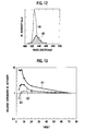
- the curve X1 indicates the case where a low temperature undoped GaN layer (film thickness 400 ⁇ ) grown at a low temperature of 750 to 800°C was used, in place of the first and second undoped InGaN layers, as a semiconductor layer between the final well layer of the active layer 6 and the p-type nitride semiconductor layer.
- the curve X2 indicates the case where a first undoped InGaN layer 7 and a second undoped InGaN layer 8 (total film thickness of 200 ⁇ ) that have no In composition gradient are used between the final well layer of the active layer 6 and the p-type nitride semiconductor layer.
- the curve X3 indicates the case where the first undoped InGaN layer 7 that has no In composition gradient and the second undoped InGaN layer 8 that has an In composition gradient (total film thickness of 200 ⁇ ) were used between the final well layer of the active layer 6 and the p-type nitride semiconductor layer. This is calculated by obtaining the relative integrated electroluminescence (EL) intensity.
- EL electroluminescence
- the integrated PL intensity for the absolute temperature 12K corresponds to the area for the curve of 12K in the drawing.
- a predetermined absolute temperature is expressed by RT
- the integrated PL intensity at the RT corresponds to the area for the curve of the RT in the drawing.
- a graph is made from the calculation of the integrated PL intensity at each temperature by changing the RT from 12K to 290K approximately.
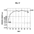
- Fig. 17 shows one example of this graph.
- the average of integrated PL intensities when the luminous efficiency is the highest is expressed by I (12K), and this I (12K) is the criterion.
- the relative integrated EL intensity at the temperature parameter RT is expressed by I (RT)/I (12K).
- Fig. 13 shows I (RT)/I (12K).
- the ordinate is the relative integrated EL intensity (relative integrated PL intensity), and the abscissa is the inverse number of the absolute temperature, resulting in Arrhenius plots.
- T in (1000/T) described in the abscissa is the absolute temperature, and its unit is K (Kelvin).
- the measurement and calculation as described above were executed, and the graphs of X1 to X3 were obtained. Note that the In composition ratios of the undoped InGaN layers which have no In composition gradient, and which were used in the measurements of X2 and X3, were all made to be 2.5% or less.
- the higher luminous efficiency means that the higher hole injection efficiency from a p-type nitride semiconductor layer of a p-type Gan-based contact layer or a p-type AlGan cladding layer.
- compared difference is only the semiconductor layer between the final well layer of the active layer 6 and the p-type nitride semiconductor layer. Therefore, which semiconductor layer is shown to increase the hole injection efficiency the most.
- the curve Y2 in Fig. 14 exhibits a curve of a relative integrated EL intensity where the same constitution used in the measurement of the curve X3 in Fig. 13 is adopted in the semiconductor layer between the final well layer of the active layer 6 and the p-type nitride semiconductor layer.
- the total film thickness of the first undoped InGaN layer that has no In composition gradient and the second undoped InGaN layer that has the In composition gradient is made 100 ⁇ that is far smaller than the total film thickness of 20 nm or less.
- the curve Y1 exhibits a curve of a relative integrated EL intensity where the barrier layer 6b is used instead of the first undoped InGaN layer, and where an undoped InGaN layer that has an In composition gradient is used as the second undoped InGaN layer.
- the total film thicknesses of the barrier layer and undoped InGaN layer is made 100 ⁇ .
- the In composition ratio of the undoped InGaN layer that has no In composition gradient was made to be 2.5% or less.
- similar undoped InGaN layers were used for the composition gradient curves of the undoped InGaN layers having the In composition gradient, which were used in the measurements of Y1 and Y2.
- a graph is drawn by taking the ordinate as the relative integrated EL intensity and the abscissa as 1000/T. Comparison of the curve Y1 with the curve Y2 shows that Y2 is higher in hole injection efficiency in almost the entire temperature range. Additionally, in a high-temperature region, the curve Y2 is shown to have its value of relative integrated EL intensity further converged to 1. This is because the film thickness of the undoped InGaN layer 7 is decreased. It is shown that, when the total film thickness of the intermediate semiconductor layers is made 200 ⁇ or less and as the total film thickness is made smaller, the hole injection efficiency is increased, thus improving the luminous efficiency.
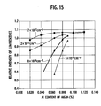
- Fig. 15 shows the relation among the Al content, the hole carrier concentration, and the emission intensity of the nitride semiconductor light emitting element, when the p-type AlGan cladding layer 12 is formed as in the constitution of Fig. 2 .
- the abscissa shows the Al composition ratio of p-type AlGaN, and the ordinate shows the emission intensity.
- Graphs of various hole carrier concentrations are drawn. When the carrier concentration becomes less than 2 ⁇ 10 17 cm -3 like the curve with a carrier concentration of 8 ⁇ 10 16 cm -3 and the curve with a carrier concentration of 5 ⁇ 10 16 cm -3 , the inclination of the curve becomes extraordinarily steeper. The emission intensity extraordinarily falls as the Al composition ratio becomes small.
- the band-gap is increased and the height of the barrier is readily secured.
- the band-gap increases, the activation yield of impurities becomes small, and the carrier concentration falls even for the same impurity concentration. Because the improvement of the carrier concentration determines the true barrier height for electrons, the range to be used properly is determined. Its use range is 0.02 ⁇ x ⁇ 0.15 for Al x GaN. When the one practically used without extraordinarily lowering the emission intensity in this range is searched, it is revealed that the carrier concentration must be at least 2 ⁇ 10 17 cm -3 .
- the above p-type AlGaN cladding layer can be formed and grown even at a substrate temperature of 950°C.
- the growth temperature of 1000°C or above is desirable as described above by improving crystallinity to thereby prevent the generation of carrier compensation effect and an increase in residual electron concentration and to maintain the hole concentration (carrier concentration) high.
- Fig. 16 shows how crystallinity changes according to the growth temperature.
- the ordinate shows the photoluminescence intensity (arbitrary unit)
- the abscissa shows the emission wavelength.
- the ordinate relatively represents the measured photoluminescence intensity (PL intensity) on the basis on the highest point among the measured photoluminescence intensities.
- This is configured by stacking undoped GaN on a sapphire substrate, and then stacking 2000 ⁇ of an AlGaN single film on the undoped GaN.
- the measurement was performed using a He-Cd laser as an excitation light source, an excitation intensity of 2.5 mW and a measurement temperature of 12K.
- K is Kelvin that shows the absolute temperature.
- the p-type AlGaN may be grown at a substrate temperature of 950°C. However, when it is grown at the substrate temperature of 950°C as shown in Fig. 16 , a phenomenon called deep-level light emission is generated. This shows that a carrier compensation effect is generated in the AlGaN, or that a new level, that is, a crystal defect is generated within the band-gap. This causes a decrease in the hole concentration. On the other hand, when the p-type AlGaN is grown at a substrate temperature of 1010°C and the crystallinity is further improved, a deep-level light emission is not generated. Thus, the hole concentration is maintained as it is, which can prevent the deterioration of the hole injection efficiency. Therefore, a growth temperature of 1000°C or above is shown to be desirable in order to further improve the crystallinity of the p-type AlGaN.
- a growth temperature of 1000°C or above is rather better to greatly improve the crystallinity of p-type AlGaN.
- its growth temperature is desirably a high temperature of at least 950°C.
- the In content of the InGaN well layer 6c in the active layer 6 becomes as large as 10% or more in a visible light LED that emits light at a peak wavelength of 410 nm or more and that uses an especially important nitride in the industry in particular.
- the In composition ratio becomes high, the In sublimates and the well layer 6c readily breaks down when the layer is placed at a high temperature, extraordinarily decreasing the luminous efficiency. Therefore, the crystallinity of a p-type Al X Ga Y N layer is improved when the p-type Al X Ga Y N is made to grow at a high temperature that exceeds 950°C.
- this causes a problem in that the In component in the already film-formed active layer having a high In composition ratio decomposes, decreasing the luminous efficiency greatly.
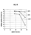
- Fig. 19 shows this state.
- the constitution of Fig. 1 or 3 described above was used as a nitride semiconductor light emitting element, and the range of the In composition ratio of the active layer 6 was changed as follows.
- a barrier layer 6b was made up of In z2 GaN (0 ⁇ z2 ⁇ 0.03) having an Si-doping concentration of 5 ⁇ 10 16 cm -3 to 5 ⁇ 10 18 cm -3 and has a film thickness of 100 to 350 ⁇ , desirably, 150 to 300 ⁇ .
- the well layer 6c is made up of, for example, non-doped In y2 GaN (0.15 ⁇ y2 ⁇ 0.18) with a film thickness of 30 ⁇ .
- the Si doping concentration is desirably 5 ⁇ 10 18 cm -3 or less.
- 3 to 8 layers, desirably 5 to 7 layers, of the well layers are formed.
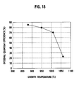
- Fig. 17 shows how the luminous efficiency of the nitride semiconductor light emitting element changes according to the growth temperature of the p-type GaN-based contact layer or the p-type AlGaN cladding layer.
- a light emitting element was formed such that the p-type GaN contact layer was a p-type GaN-based contact layer in the constitution of Fig. 1 , that its growth temperature was kept constant, and that the growth time of the p-type GaN contact layer was 27 minutes. Thereafter, the internal quantum efficiency was measured. In addition, the internal quantum efficiency at each growth temperature was measured by changing the growth temperature of the p-type GaN contact layer.
- the growth temperature was set at 880°C in a first measurement, at 950°C in a second measurement, at 1010°C in a third measurement and at 1060°C in a fourth measurement.
- the abscissa shows the growth temperature of the p-type GaN contact layer, and the ordinate shows the internal quantum efficiency (%) of the light emitting element.
- the internal quantum efficiency is obtained as follows.
- the integrated PL (photoluminescence) intensity (area of the curve 12K in the drawing) at an absolute temperature of 12K (K shows Kelvin) is represented by J (12K).
- This integrated PL intensity is set to be I (290K).
- the integrated PL intensities at sample temperatures of several points from 12K to 290K are obtained and plotted to draw graphs as shown in Fig. 13 .
- the abscissa of Fig. 17 is the inverse number of the absolute temperature, resulting in an Arrhenius plot.
- the average of integrated PL intensities when the luminous efficiency is the highest is expressed by I (12K), and this I (12K) is the criterion.
- the growth temperature at which the InGaN well layer 6c of the active layer 6 is not deteriorated while the p-type GaN layer and the p-type AlGaN layer are kept to have good crystallinity, is desirably between 950°C and 1010°C.
- the p-type GaN contact layer 8 was made to be a p-type GaN-based contact layer 8 in the constitution of Fig. 1 .
- the In content of the well layer 6c in the nitride semiconductor light emitting element was made to be 10% or more. Then, the relationship between the internal quantum efficiency and the growth time from completion of the formation of the well layer closest to the p-side among the well layers in the active layer 6 until completion of the formation of the p-type GaN contact layer was determined. The results are shown in Fig. 19 .
- the abscissa shows the above growth time, and the ordinate shows the internal quantum efficiency.
- the growth temperature from the completion of the formation of the well layer closest to the p-side until the completion of the formation of the p-type GaN contact layer was changed to 900°C at a first time, to 950°C at a second time and to 1010°C at a third time, and the measurement was carried out at each growth temperature.
- the growth time from the completion of the formation of the well layer closest to the p-side until the completion of the formation of the p-type GaN contact layer refers to the total of the growth times of the first undoped InGaN layer 7, the second undoped InGaN layer 8 and the p-type GaN contact layer, in the constitution of Fig. 1 .
- the growth time refers to the total of the growth times of the first undoped InGaN layer 7, the second undoped InGaN layer 8, the p-type AlGaN cladding layer 12 and the p-type GaN contact layer.
- the intermediate measurement point indicates a growth time of 27 minutes.
- the growth temperature is 900°C
- the effect on the emission intensity is negligible even if the growth time is long.
- the growth temperature becomes 950°C or above and the growth time is long the emission intensity is shown to be extraordinarily decreased. This is because, when the time during which the InGaN well layer 6c of the active layer 6 is heated at a high temperature becomes long, the layer is deteriorated due to the sublimation of In, and the like.
- 30 minutes is a limit of the total growth time.
- the p-type AlGaN cladding layer is added to the constitution of Fig. 1 . Therefore, in addition to the growth time of the p-type AlGaN cladding layer, the total time when the growth temperature is 950°C or above must be within 30 minutes.
- a method of manufacturing the nitride semiconductor light emitting elements of Figs. 1 and 3 when the In content of the InGaN well layer 6c in the active layer 6 is 10% or more, that is, the peak wavelength is 410 nm or more will be described.
- This method is basically similar to the above-described method.
- the layer of interest whose growth temperature becomes 950°C or above is only the p-type GaN-based contact layer 9. This corresponds to the fact that the growth time of the p-type GaN-based contact layer 9 is made within 30 minutes.
- the layer of interest whose growth temperature becomes 950°C or above is the p-type AlGan cladding layer 12 and the p-type GaN-based contact layer 9. The total growth time of these two layers only has to be within 30 minutes.
- the layer of interest whose growth temperature becomes 950°C or more is only the p-type Gan-based contact layer 9. This corresponds to the fact that the growth time of the p-type Gan-based contact layer 9 is made within 30 minutes.
- the layer of interest whose growth temperature becomes 950 °C or more is the p-type AlGan cladding layer 12 and the p-type Gan-based contact layer 9. The total of the growth times of these two layers only has to be within 30 minutes.
- the carrier compensation center can also be reduced as much as possible by heating the undoped InGaN layer 7 at a high temperature of 950°C or above instead of the growth temperature of approximately 750°C to remove the convexoconcave on the surface as much as possible.
- the film thickness of each layer must be adjusted now in order to make the total time when the growth temperature is 950°C or above be within 30 minutes.
- the manufacturing method described above uses a p-type GaN layer as the p-type Gan-based contact layer 9 in the constitution of Fig. 1 .
- the growth temperature is increased to 1000 to 1030°C (e.g., 1010°C), and the film is grown to, for example, 700 ⁇ . Nevertheless, particularly in a green LED or the like having a high In content, the InGaN well layer 6c is pyrolyzed even at this temperature. Therefore, in this case, the growth temperature of the p-type GaN-based contact layer 9 is suppressed to 800 to 900°C.
- a p-type InGaN layer doped with Mg that can exhibit a high hole carrier concentration at this growth temperature is used as the p-type GaN-based contact layer 9.
- the In composition ratio of the p-type InGaN layer is determined by the growth temperature, but is sufficient when approximately 0.5% to 3%.
- the total growth time when the growth temperature exceeds 950°C can be made to be O from the completion of the formation of the well layer closest to the p-type nitride semiconductor layer among the well layers in the active layer 6 until the completion of the formation of the p-type GaN-based contact 8.
- This is effective means especially for a green LED with a high In content, or the like.
- the p-type AlGan cladding layer 12 is formed to have a thickness of 200 ⁇ , for example.
- AlGaN is made to grow at a temperature of approximately 950°C, desirably approximately 1000°C or above.
- the growth time at 950°C or above is adjusted to be within 30 minutes by increasing the formation speed or decreasing the film thickness of the p-type GaN-based contact layer 8. If possible, 15 minutes or less is desirable.
Landscapes
- Led Devices (AREA)
- Semiconductor Lasers (AREA)
Abstract
Provided is a nitride semiconductor light emitting element having an improved carrier injection efficiency from a p-type nitride semiconductor layer to an active layer by simple means from a viewpoint utterly different from the prior art. A buffer layer 2, an undoped GaN layer 3, an n-type GaN contact layer 4, an InGaN/GaN superlattice layer 5, an active layer 6, a first undoped InGaN layer 7, a second undoped InGaN layer 8, and a p-type Gan-based contact layer 9 are stacked on a sapphire substrate 1. A p-electrode 10 is formed on the p-type Gan-based contact layer 9. An n-electrode 11 is formed on a surface where the n-type GaN contact layer 4 is exposed as a result of mesa-etching. The first undoped InGaN layer 7 is formed to contact a well layer closest to a p-side in the active layer having a quantum well structure, and subsequently the second undoped InGaN layer 8 is formed thereon. The carrier injection efficiency into the active layer 6 can be improved by making the total film thickness of the first and second undoped InGaN layers 20 nm or less.
Description
- The present invention relates to a nitride semiconductor light emitting element including an active layer which has a quantum well structure with a well layer made of a nitride containing In.
- Recently, short-wavelength semiconductor lasers have been intensively developed for the application of the semiconductor lasers in high density optical disk recording and the like. Hexagonal compound semiconductors including nitrogen (hereinafter, simply called nitride semiconductors) such as GaN, AlGaN, InGaN, InGaAlN and GaPN are used for short wavelength semiconductor lasers. In addition, LEDs using nitride semiconductors also have been developed.
- As the nitride semiconductor light emitting elements, light emitting elements of the MIS structure have been used in some cases. However, such a light emitting element has a high-resistance i-type GaN-based semiconductor stacked thereon, and accordingly has a problem of generally very low emission output. To solve such a problem, the i-type GaN-based semiconductor layer is irradiated with electrons or is annealed.
- Additionally, even for a nitride semiconductor light emitting element having a p-type GaN-based semiconductor layer formed therein, efforts are made to increase the emission output. For example, in order to improve the luminous efficiency, it is proposed, as disclosed in
Patent Document 1, that the forward voltage Vf be reduced by forming an ohmic contact between a p-electrode and a p-type GaN contact layer or by making smaller the film thickness of a p-type GaN contact layer. - Moreover, in order to improve the luminous efficiency,
Patent Document 1 also proposes that Mg be used as a p-type dopant to obtain the p-type characteristics of a p-type AlGaN cladding layer, or that the film thickness and the Al composition of the p-type AlGaN cladding layer be specified to improve the crystallinity. - Patent Document 1: Japanese Patent No.
2778405 - However, even if the luminous efficiency is improved by the above prior art: by the improvements in the respective attributes of the ohmic contact between the p-electrode and the p-type GaN contact layer; the film thickness of the p-type GaN contact layer; the p-type dopant; and the crystallinity of the p-type AlGaN cladding layer, the effects from these improvements are limited. In addition, effective means for further increasing the luminous efficiency is not yet to be obtained.
- The present invention has been created to solve the problems mentioned above. An object of the present invention is to provide a nitride semiconductor light emitting element having an improved carrier injection efficiency from a p-type nitride semiconductor layer to an active layer and an improved luminous efficiency by simple means from a viewpoint utterly different from the prior art.
- A nitride semiconductor light emitting element of the present invention is a nitride semiconductor light emitting element with a structure in which an active layer is sandwiched between a p-type nitride semiconductor layer and an n-type nitride semiconductor layer, the active layer having a quantum well structure with a well layer made of a nitride containing In. The summary thereof is that a first undoped InGaN layer and a second undoped InGaN layer with an In content different from that of the first undoped InGaN layer are formed between the p-type nitride semiconductor layer and the well layer of the active layer disposed at a position closest to a p-side, and that a total film thickness of the first undoped InGaN layer and the second undoped InGaN layer is 20 nm or less.
- We have found means utterly different from the above prior art as means for improving the hole injection efficiency from the p-type semiconductor layer to the active layer. In other words, it has been found that the hole injection efficiency from the p-type nitride semiconductor layer to the active layer is drastically changed when two undoped InGaN layers with different In composition ratios from each other are formed between the p-type nitride semiconductor layer and the well layer of the active layer disposed at the position closest to the p-type side, and when the total film thickness of these undoped InGaN layers becomes 20 nm or less.
- Moreover, another summary is that, when the second undoped InGaN layer is formed between the first undoped InGaN layer and the p-type nitride semiconductor layer, the second undoped InGaN layer is an In composition gradient layer whose In content decreases toward the p-type nitride semiconductor layer.
- Moreover, other summary is that, when Mg-doped p-type AlxGaN (0.02≤x≤0.15) is formed as a part of the p-type nitride semiconductor layer, the hole carrier concentration is made to be in a range of 2×1017 cm-3 or more.
- In addition to the above-described summaries, the other summary of the nitride semiconductor light emitting element of the present invention is that, when the well layer of the active layer has an In composition ratio of 10% or more and thus the emission wavelength becomes long, a total film formation time when a growth temperature exceeds 950°C is within 30 minutes from the time of completion of the formation of the final well layer of the active layer in a growth direction to the time of completion of the formation of a p-type contact layer that is formed as a part of the p-type nitride semiconductor layer, and that is in contact with a p-electrode. In particular, InGaN is thermally unstable and thus there arises a possibility of its decomposition when the above conditions are exceeded. In the worst case, the In is dissociated and the wafer is blackened.
- In the nitride semiconductor light emitting element of the present invention, two undoped InGaN layers with different In contents from each other are formed between the p-type nitride semiconductor layer and the well layer of the active layer closest to the p-type side having the quantum well structure. The total film thickness of these two undoped InGaN layers is formed to be 20 nm or less. Thereby, the injection efficiency of holes into the active layer can be greatly improved, thus improving the luminous efficiency.
- Of the two undoped InGaN layers, the undoped InGaN layer closer to the p-type nitride semiconductor layer is made to be an In composition gradient layer whose In content decreases toward the p-type nitride semiconductor layer. This makes it easy to inject holes into the active layer, thus improving the luminous efficiency.
- Moreover, the p-type AlxGaN (0.02≤x≤0.15) is stacked on the two undoped InGaN layers and is formed such that the hole carrier concentration due to p-type impurities becomes 2x1017 cm-3 or more. Thereby, the amount of holes injected into the active layer can be obtained sufficiently, and thus the luminous efficiency can be improved.
- In addition, the total film formation time when the growth temperature is 950°C or above is made to be within 30 minutes from the time of completion of the formation of the final well layer of the active layer in the growth direction to the time of the completion of the formation of the p-type contact layer that is formed as a part of the p-type nitride semiconductor layer, and that is in contact with the p-electrode. Thereby, in a nitride semiconductor light emitting element of a comparatively long emission wavelength, in other words, when a well layer of an active layer has an In composition ratio of 10% or more, the degradation of the active layer can be prevented, and thus a high emission intensity can be maintained.
-
- [
Fig. 1] Fig. 1 is a diagram indicating a cross-sectional structure of a first nitride semiconductor light emitting element of the present invention. - [
Fig. 2] Fig. 2 is a diagram indicating a layer structure in the vicinity of an active layer. - [
Fig. 3] Fig. 3 is a diagram indicating a cross-sectional structure of a second nitride semiconductor light emitting element of the present invention. - [
Fig. 4] Fig. 4 is a diagram indicating the relationship between the total film thickness of undoped InGaN layers and the luminance of the nitride semiconductor light emitting element. - [
Fig. 5] Fig. 5 is a diagram indicating an emission spectrum when the film thickness of the undoped InGaN layers is 350Å. - [
Fig. 6] Fig. 6 is a diagram indicating an emission spectrum when the film thickness of the undoped InGaN layers is 120Å. - [
Fig. 7] Fig. 7 is a diagram indicating the relationship between the In composition of the undoped InGaN layer and the luminance of the nitride semiconductor light emitting element. - [
Fig. 8] Fig. 8 is a diagram indicating a state of a band-gap energy in the vicinity of an active layer. - [
Fig. 9] Fig. 9 is a diagram indicating a state of a band-gap energy in the vicinity of the active layer, the vicinity being different from that inFig. 8 . - [
Fig. 10] Fig. 10 is a diagram indicating the relationship between the relative ratio of In flow rate at each growth temperature and the In composition ratio of the InGaN layer. - [
Fig. 11] Fig. 11 is a diagram indicating the relationship between the growth temperature of the InGaN layer and the In composition ratio. - [
Fig. 12] Fig. 12 is a conceptual diagram for calculating the relative integrated EL intensity. - [
Fig. 13] Fig. 13 is a diagram indicating a state where the relative integrated EL intensities vary due to the kind of semiconductor layers formed between a final well layer of an active layer and a p-type nitride semiconductor layer. - [
Fig. 14] Fig. 14 is a diagram indicating a state where the relative integrated EL intensities vary due to the semiconductor layers formed between the final well layer of the active layer and the p-type nitride semiconductor layer. - [
Fig. 15] Fig. 15 is a diagram indicating the relationship between the Al composition ratio of AlGaN and the luminance of the nitride semiconductor light emitting element. - [
Fig. 16] Fig. 16 is a diagram indicating the relationship between the growth temperature of AlGaN and the emission spectrum. - [
Fig. 17] Fig. 17 is a diagram indicating a state where a value obtained by integration of PL intensity varies with temperature. - [
Fig. 18] Fig. 18 is a diagram indicating the relationship between the growth temperature and the internal quantum efficiency of the p-type nitride semiconductor layer. - [
Fig. 19] Fig. 19 is a diagram indicating the relationship between the growth time and the internal quantum efficiency at each growth temperature of the p-type nitride semiconductor layer. -
- 1: Sapphire substrate
- 2: Buffer layer
- 3: Undoped GaN layer
- 4: N-type GaN contact layer
- 5: InGaN/GaN superlattice layer
- 6: Active layer
- 6b: Barrier layer
- 6c: Well layer
- 7: First undoped InGaN layer
- 8: Second undoped InGaN layer
- 9: P-type GaN-based contact layer
- 10: P-electrode
- 11: N-electrode
- 12: P-type AlGaN cladding layer
-
Fig. 1 shows a cross-sectional view of one example of a first nitride semiconductor light emitting element of the present invention. On asapphire substrate 1, stacked are abuffer layer 2, anundoped GaN layer 3, an n-typeGaN contact layer 4, an InGaN/GaN superlattice layer 5, anactive layer 6, a firstundoped InGaN layer 7, a secondundoped InGaN layer 8 and a p-type GaN-basedcontact layer 9. A region of the first nitride semiconductor light emitting element is partially mesa-etched from the p-type GaN-basedcontact layer 9, and an n-electrode 11 is formed on a surface where the n-typeGaN contact layer 4 is exposed. In addition, a p-electrode 10 is formed on the p-type GaN-basedcontact layer 9. Here, the p-type GaN-based layer is made up of GaN having doped therein p-type impurities or a compound including GaN. The undoped InGaN layer is made up of an InGaN layer in which no impurities are intentionally doped. - As stated above, the n-type
GaN contact layer 4 and the InGaN/GaN superlattice layer 5 are formed as n-type nitride semiconductor layers. The p-type GaN-basedcontact layer 9 is formed as a p-type nitride semiconductor layer. The nitride semiconductor light emitting element of the present invention has a double heterostructure with these n-type nitride semiconductor layers and the p-type nitride semiconductor layer sandwiching the active layer. - In the
buffer layer 2, GaN, AlN, Alx1GaN (0<x1≤0.1) or the like is used. Thebuffer layer 2 is formed in a film thickness of from 50 to 300Å, desirably from 100 to 200Å. Theundoped GaN layer 3 stacked on thebuffer layer 2 has a film thickness of 1 to 3 µm. The n-typeGaN contact layer 4 formed on theundoped GaN layer 3 has a Si doping concentration of 1x1018 cm-3 to 5x1018 cm-3 and has a film thickness of 1 to 5 µm. Additionally, the InGaN/GaN superlattice layer 5 relaxes the stress of InGaN and GaN that have a large difference in lattice constant from each other. The InGaN/GaN superlattice layer 5 causes the InGaN of theactive layer 6 to grow readily. The InGaN/GaN superlattice layer 5 to be used has a constitution, for example, in which InxGaN (0.03≤x≤0.1) having a Si doping concentration of 1×1018 cm-3 to 5×1018 cm-3 and a film thickness of 10Å and GaN having a film thickness of 20Å are alternately stacked on each other at approximately 10 repetitions. - The
active layer 6 is an active layer that has a quantum well structure (Quantum Well) and has a structure in which a well layer is sandwiched with barrier layers each having a larger band-gap than the well layer. This quantum well structure may not only be a single structure, but be a multiplexed structure. In this multiplexed case, the structure becomes a MQW (Multi-Quantum Well), namely, a multiquantum well structure. Moreover, theactive layer 6 is made up of a ternary mixed crystal system of InGaN. The firstundoped InGaN layer 7 is formed to contact the final well layer of theactive layer 6 in a growth direction. The firstundoped InGaN layer 7 has a role of a barrier layer or a cap layer of theactive layer 6. -
Fig. 2 shows the structure of theactive layer 6 in detail. Abarrier layer 6b is disposed on a side of the InGaN/GaN superlattice layer 5 where theactive layer 6 contacts the InGaN/GaN superlattice layer 5. Awell layer 6c is stacked on thebarrier layer 6b. Thisbarrier layer 6b and thewell layer 6c are alternately stacked on each other at a number of repetitions. Thereafter, the firstundoped InGaN layer 7 is stacked on thefinal well layer 6c so as to be in contact with each other. The secondundoped InGaN layer 8 is formed on the firstundoped InGaN layer 7. The p-type Gan-basedcontact layer 9 is formed on the secondundoped InGaN layer 8. - Here, the
barrier layer 6b is made up of Inz1GaN (O≤z1<1) either being non-doped or having an Si doping concentration of 5×1016 cm-3 to 5×1018 cm-3 and has a film thickness of 100 to 350Å, and desirably of 150 to 300Å. On the other hand, thewell layer 6c may be made up of, for example, non-doped Iny1GaN (0<y1<1, y1>z1) with a film thickness of 30Å. However, when the impurities are doped therein, the Si doping concentration is desirably 5×1018 cm-3 or less. In addition, 3 to 8 layers, desirably 5 to 7 layers, of the well layers are formed. In theactive layer 6, the emission wavelength can be changed from purple to red by allowing the above y1 to be in a range of 0<y1<1. - In addition, the total film thickness of: the first
undoped InGaN layer 7 formed to contact the final well layer of theactive layer 6; and the secondundoped InGaN layer 8 formed to contact the firstundoped InGaN layer 7 is made to be 20 nm or less. The firstundoped InGaN layer 7 has roles as an electron barrier layer that makes no electrons flow from theactive layer 6 to the p-side and also as a cap layer of preventing the In of thewell layer 6c from sublimating at high temperatures, the sublimating consequently causing thewell layer 6c to readily break down. Hence, the firstundoped InGaN layer 7 desirably has a band-gap energy equal to or more than that of thebarrier layer 6b in order to have a band-gap energy larger than that of thewell layer 6c and to thereby block electrons. ThisInGaN layer 7 is desired to be an InGaN layer with an In composition ratio of z1 or less. The secondundoped InGaN layer 8 desirably has a band-gap energy larger than that of the firstundoped InGaN layer 7 but smaller than that of the p-type Gan-basedcontact layer 9. Therefore, the In composition ratio of the secondundoped InGaN layer 8 is desirably smaller than that of the firstundoped InGaN layer 7 in a range excluding 0. - P-type InGaN or p-type GaN is used for the p-type Gan-based
contact layer 9 formed on the secondundoped InGaN layer 8. Thiscontact layer 9 has a Mg-doping concentration of 3×1019 cm-3 to 3×1020 cm-3, and is grown to have a film thickness of approximately 200 to 3000Å (most desirably, 700Å to 1000Å). -
Fig. 4 shows a manner in which the luminance changes according to the total film thickness of the firstundoped InGaN layer 7 and the secondundoped InGaN layer 8. The emission intensity (luminance) was measured by changing the total film thickness of the firstundoped InGaN layer 7 and the secondundoped InGaN layer 8 in constitution ofFig. 1 . The abscissa indicates the total film thickness of the two undoped InGaN layers. The ordinate indicates relative luminances based on the luminance at 250Å. When the total film thickness becomes 200Å (20 nm) or less, the luminance is shown to be greatly improved. - This reason can be discussed as follows.
Fig. 5 shows an emission spectrum when the total film thickness of the two undoped InGaN layers is 350Å in the constitution ofFig. 1 . The ordinate indicates relative luminances based on the emission intensity of a standard LED. InFig. 5 , not only an original emission spectrum of theactive layer 6 but also a spectrum of the undoped InGaN layer is also shown together. The recombination of a hole and an electron is generated not only in theactive layer 6 but also in the undoped InGaN layers. The luminous efficiency of theactive layer 6 decreases because holes are not sufficiently transferred from the p-type Gan-basedcontact layer 9 to theactive layer 6. - On the other hand,
Fig. 6 shows an emission spectrum when the total film thickness of the undoped InGaN layers is 120Å. Only an original emission spectrum of theactive layer 6 appears, but a spectrum of the undoped InGaN layer as inFig. 5 does not appear. This is because, when the total film thickness of the undoped InGaN layers is smaller, the injection efficiency of holes from the p-type Gan-basedcontact layer 9 into theactive layer 6 is improved. Therefore, the undoped InGaN layers with a smaller total film thickness lead to a larger emission intensity of the light emitting element. In addition, it can be recognized fromFig. 4 that the optimum value of this total film thickness is 200Å (20 nm) or less. - Next,
Fig. 3 shows a constitution of a second nitride semiconductor light emitting element of the present invention. The constituents denoted by the same symbols as those inFig. 1 are shown to have the same constitutions as those inFig. 1 . The difference between the second nitride semiconductor light emitting element and the first nitride semiconductor light emitting element is that a p-typeAlGan cladding layer 12 is inserted between the secondundoped InGaN layer 8 and the p-type Gan-basedcontact layer 9. The p-typeAlGan cladding layer 12 has a role of an electron barrier layer, and aims to further improve the injection efficiency of holes. As the p-typeAlGan cladding layer 12, p-type AlxGaN (0.02≤x≤0.15) or the like is used. The carrier concentration of the p-type AlxGaN obtained by doping the impurity Mg therein is desirably in a range that is 2×1017 cm-3 or more as described below. The p-typeAlGan cladding layer 12 is made up of Al0.07GaN with a film thickness of 150 to 300Å (most desirably 200Å). - In the second nitride semiconductor light emitting element (constitution of
Fig. 3 ), the luminance was measured by changing the total film thickness of the two undoped InGaN layers. In this case also, the graphical form shown inFig. 4 was obtained. Hence, with the constitution ofFig. 3 also, when the total film thickness of the undoped InGaN layers becomes 200Å or less, the luminance is greatly improved. - On the other hand,
Fig. 7 shows the relationship between the In composition ratio of the undoped InGaN layer and the luminance of the nitride semiconductor light emitting element. The abscissa shows the In composition ratio, and the ordinate shows the luminance (arbitrary unit). The ordinate indicates relative luminances based on the luminance measured when the In composition ratio is 0.5%. The luminances were measured in the constitutions ofFigs. 1 and3 . As can be seen from the drawing, the In composition ratio of up to approximately 2.5% can be used for light-emission luminance. Meanwhile, as the ratio becomes more than 2.5%, the light-emission luminance considerably approaches 0, and the ratio of more than 2.5% is not usable. This is because InGaN originally has a large residual electron concentration, and therefore the residual electron concentration is also increased when the In composition ratio is raised. For this reason, it is recognized that, in order to increase the amount of carriers (holes) to be injected, the In composition ratio is desired to be small. In addition, it is shown that, when the In content is approximately 0.5% to 1%, the highest luminance condition can be maintained. Therefore, in the firstundoped InGaN layer 7 and the secondundoped InGaN layer 8, the In composition ratio is desirably 2.5% or less, most suitably in a range of 0.5% to 1%. -
Fig. 8 shows one example of the constitution of the firstundoped InGaN layer 7 and the secondundoped InGaN layer 8, with different In compositions from each other, using a band-gap energy diagram of conduction bands. The firstundoped InGaN layer 7 plays a role as an electron barrier layer. This layer is configured to have a band-gap energy equal to or more than the band-gap energy of thebarrier layer 6b. In addition, the secondundoped InGaN layer 8 is configured to have a band-gap energy larger than that of the firstundoped InGaN layer 7 but smaller than that of the p-type Gan-basedcontact layer 9. Here, from the result ofFig. 7 , both the firstundoped InGaN layer 7 and the secondundoped InGaN layer 8 are formed so as to have an In composition ratio of 2.5% or less. - As described above, when the first and second undoped InGaN layers are formed, the first and second undoped InGaN layers can be configured to have stepwise increased band-gaps in the order the first
undoped InGaN layer 7, the secondundoped InGaN layer 8 and the p-type nitride semiconductor layer, as shown inFig. 8 . - Next, description will be given below of a case where the second
undoped InGaN layer 8 is an In composition gradient layer.Fig. 9 shows a band-gap energy diagram of conduction bands in front and back of theactive layer 6. Thebarrier layer 6b and thewell layer 6c form a quantum well structure. The firstundoped InGaN layer 7 is formed on the p-side to contact thefinal well layer 6c. The secondundoped InGaN layer 8 is formed to contact this firstundoped InGaN layer 7. The In composition ratio of this secondundoped InGaN layer 8 decreases continuously from the junction with the firstundoped InGaN layer 7 toward the direction of the p-type nitride semiconductor layer (rightward in the drawing). The decrease in the In composition ratio toward the p-type nitride semiconductor layer means that the band-gap energy of the secondundoped InGaN layer 8 increases toward the p-type nitride semiconductor layer. - If the In composition is changed with the gradient, as shown in
Fig. 9 , the band structure in the conduction band that serves in hole conduction has a lower potential toward the well layer. Thus, it is desirable because holes easily flow thereinto. Moreover, because the residual electron concentration decreases when the growth temperature is high, the composition gradient of In is desirably fabricated at a high growth temperature. - Next, description will be given of methods of manufacturing the first and second nitride semiconductor light emitting elements. A PLD method (laser ablation method) is used for forming the
buffer layer 2 made of single crystals such as GaN, AlN and Alx1GaN (0<X1≤0.1) on thesapphire substrate 1. - First, the
sapphire substrate 1 is placed in a load lock chamber and heated at a temperature of approximately 400°C for 5 to 10 minutes to remove excess moisture and the like. Thereafter, thesapphire substrate 1 is transported into a vacuum chamber with an internal pressure of 1×10⁻⁶ Torr or less and is placed so as to oppose a target. Thesapphire substrate 1 is placed on a heat source, and the substrate temperature is maintained at 600°C to 1000°C. For example, the target is irradiated with the KrF excimer laser light having an oscillation wavelength of 248 nm from a quartz window of the vacuum chamber to thereby sublimate (ablate) the material of the target. This sublimated atom adheres to the surface of thesapphire substrate 1, and thebuffer layer 2 of single crystal grows up. Thebuffer layer 2 forms into a thickness of, for example, 100Å to 200Å. - A sintered GaN target is used as the target. Of course, a sintered body target of AlN, AlGaN, or InGaN may be used. However, when a sintered body target is used, it is difficult to determine a composition, since a sintered body target of InGaN is a substance into which In is hardly incorporated in general. Therefore, a sintered body target of GaN, AlN or AlGaN is desired.
- Next, the
sapphire substrate 1 having thebuffer layer 2 formed thereon as described above is placed in a load lock chamber of an MOCVD apparatus. This substrate is heated for 5 to 10 minutes at a temperature of approximately 400°C to remove excess moisture and the like, and then transported to a reaction chamber of the MOCVD apparatus. The substrate is subjected to thermal cleaning in the MOCVD apparatus at 1100°C for 30 minutes in an NH3 atmosphere. - Next, the
undoped GaN layer 3 is stacked. The substrate temperature is increased to 1065°C. For example, undoped GaN is grown to 1 µm, and Si-doped n-type GaN is grown to 2.5 µm. The substrate temperature is lowered to 760 °C, and the InGaN/GaN superlattice layer 5 is formed to, for example, 300Å. The substrate temperature is lowered to 750°C, and theactive layer 6 is formed to, for example, 3/17 nm. - After the final well layer is made to grow, the first
undoped InGaN layer 7 and the secondundoped InGaN layer 8 are stacked thereon. The total film thickness of the firstundoped InGaN layer 7 and the secondundoped InGaN layer 8 is made to be 20 µm or less. The firstundoped InGaN layer 7 and the secondundoped InGaN layer 8 are film-formed to, for example, approximately 20 to 30Å. When the secondundoped InGaN layer 8 is not an In composition gradient layer, the In content of the first and second InGaN layers is made to be 2.5% or less, as can be recognized fromFig. 7 , but most suitably from approximately 0.5% to 1%. - Next, for the constitution of
Fig. 1 , a p-type GaN layer is made to grow to, for example, 700Å as the p-type Gan-basedcontact layer 9 by increasing the growth temperature to 1000 to 1030°C (e.g., 1010°C). In addition, as described below, an Mg-doped p-type InGaN layer may be used. In this case also, this layer is made to grow to, for example, 700Å. - After a natural oxide film is removed from the surface of the p-type Gan-based
contact layer 9 with hydrochloric acid, a multi-level metal film such as Ti/Au is formed as the p-electrode 10 by deposition or sputtering. Next, a mesa pattern is formed, and the GaN-based semiconductor laminated body is etched until the n-typeGaN contact layer 4 is exposed therefrom. At this time, it is preferable to simultaneously form a pattern in which a pillar may stand in the mesa periphery, and to treat the surface of the n-typeGaN contact layer 4 as if roughened because a large amount of light is extracted. However, in a case where the surface roughening is not executed, a sufficient etching depth is where the n-typeGaN contact layer 4 is exposed. In a case where the surface roughening is executed, it is preferable to perform the etching up to a depth that is deeper by 1 µm or more than the exposure surface of the n-typeGaN contact layer 4 because a large amount of light is extracted. - After completion of the mesa etching, Al is formed on the n-type
GaN contact layer 4 as the n-electrode 11, and is subjected to annealing at 500°C to 700°C to obtain an ohmic behavior. Thus, the constitution ofFig. 1 is completed. - Incidentally, the p-
electrode 10 is not formed on the p-type Gan-basedcontact layer 9, but the p-electrode 10 may be formed thereon after a ZnO electrode is stacked on the p-type Gan-basedcontact layer 9. In this case, a Ga-doped ZnO electrode is formed on the p-type Gan-basedcontact layer 9 by, for example, MBE (Molecular beam epitaxy) or PLD (Pulsed Laser Deposition). At this time, because the current spreading is not obtained when the specific resistance of ZnO is high, the specific resistance needs to be at least 1×10⁻³ Ωcm or less, desirably 1×10⁻⁴ Ωcm to 5×10⁻⁴ Ωcm. After this, it is preferable to form convexoconcave also on the ZnO surface like on the surface of the above-mentioned n-type GaN contact layer - Etching is performed till the p-type Gan-based
contact layer 9 by use of wet etching with hydrochloric acid or dry etching such as RIE in order to make the ZnO electrode have predetermined dimensions. Thereafter, the entire ZnO is covered with an insulator such as SiN, SiON, SiO2, Al2O3 or ZrO2. - Subsequently, the mesa-etching is performed as described above, and the n-
electrode 11 is formed on the n-typeGaN contact layer 4. After that, a contact hole is formed by partially perforating the surface of the ZnO electrode. Ti/Au or the like is formed as the p-electrode so that the Ti/Au or the like can contact the ZnO electrode through the contact hole. At this time, Ti/Au is put also on the Al as the n-electrode simultaneously, making a metal for wire bonding. Thereafter, the entire mesa is covered with an insulator such as SiN, SiON, SiO2, Al2O3 or ZrO2. Permissibly, the metal portion is perforated, and thesapphire substrate 1 is reduced in thickness to then make a chip. - Next, for the constitution of
Fig. 3 , prior to formation of the p-type Gan-basedcontact layer 9, namely, after the formation of theactive layer 6, the p-typeAlGan cladding layer 12 is formed to, for example, 200Å. AlGaN may be grown at a temperature of approximately 950°C. For further improvement of crystallinity, the growth is desirably carried out at approximately 1000°C or above. The rest of layers are formed as described above. - Next, description will be given of a method of producing an undoped InGaN layer when the second
undoped InGaN layer 8 is constituted by an In composition gradient layer that has a In composition gradient as shown inFig. 9 . Generally, when an undoped InGaN layer is made to grow, trimethylindium (TMI), triethylgallium (TEG), nitrogen (N2), NH3, and H2 are supplied to the growing room. When the In composition ratio is to be increased or decreased, the flow rate (supply ratio) of trimethylindium is generally increased or decreased at a constant temperature. - However, when a wide range of the In composition ratio is to be covered as shown in
Fig. 10 , the wide range of the In composition ratio cannot be controlled only by controlling the supply ratio of trimethylindium.Fig. 10 shows the relationship between the relative ratio of the flow rate of trimethylindium and the In composition ratio when InGaN is made. The relative ratio of the flow rate of trimethylindium is a ratio between: a certain flow rate arbitrarily determined and set at 1; and each TMI flow rate. This is depicted in the graph at each specific growth temperature. - For example, when the relative ratio of the TMI flow rate becomes approximately 0.2 or less, the In content is shown to greatly change toward 0. Controlling the In composition ratio within this range becomes difficult. For this reason, utilized is the presence of the region where the In composition ratio hardly changes even if the supply ratio of trimethylindium is increased or decreased. As a result, the In composition gradient layer having a wide range of the composition ratio is easily constituted.
- As is apparent from
Fig. 10 , at each growth temperature, even if the supply ratio of trimethylindium is increased or decreased, the In composition ratio is at its maximum point when the relative ratio of the TMI flow rate is around an S point of the drawing (approximately 1.3). - Then, the S point is taken, for example, as the value of the relative ratio of the TMI flow rate of the region where the In composition ratio hardly changes. The In composition ratios of the curves of the respective growth temperatures corresponding to the S point are set to be P1, P2, P3, and P4 with the relative ratio of the TMI flow rate being fixed at the S point. As a result, at least the In composition ratio is shown to be changed from P1 to P4, that is, from approximately 18.5% to approximately 8% when the growth temperature is changed from 770°C to 840°C.
-
Fig. 11 shows a graph obtained by plotting the In composition ratios when the relative ratio of the TMI flow rate is fixed at the S point and when the growth temperature is changed from 770°C to 840°C and to a higher temperature, as in the above manner. The abscissa ofFig. 11 shows the growth temperature of the undoped InGaN, and the ordinate shows the In composition ratio of the undoped InGaN. - As described above, the wide range from larger to smaller In composition ratios can be obtained as the growth temperature is increased without changing the relative ratio of the TMI flow rate. In addition, the In composition gradient layer can be easily produced.
- The final well layer of the
active layer 6 is made to grow at a growth temperature of 750°C in the constitution of Fig. - 1. Thereafter, when a Mg-doped p-type InGaN layer is formed as the p-type Gan-based
contact layer 9, the growth temperature should be increased to approximately 850°C. Therefore, an undoped InGaN layer that has an In composition gradient can be formed automatically in the process of increasing the temperature up to the growth temperature. Specifically, when the growth temperature is sequentially and linearly increased up to approximately 850°C, an undoped InGaN layer with a composition gradient curve as shown inFig. 11 is formed. Moreover, in the constitution ofFig. 3 , when the p-typeAlGan cladding layer 12 is made to grow at a temperature of approximately 950°C, a gradient curve up to the growth temperature of approximately 950°C can be obtained in the composition gradient curve shown inFig. 11 . - As stated above, which range of the composition gradient curve shown in
Fig. 11 is used is determined by the starting point and the completion point of the growth temperature. When the change in the In composition ratio of the In composition gradient layer needs to be continuously made, for example, from 18 to 3%, the growth temperature should be changed from T1 to T2. When the change in the In composition ratio needs to be continuously made from 3% to 0.5, the growth temperature should be changed from T2 to T3. As described above, the residual concentration of electrons decreases when the growth temperature is high. Therefore, the In composition gradient layer is desirably made at a higher growth temperature. In addition, the starting point of the growth temperature should also be set high. - Incidentally, luminous efficiencies were compared when three kinds of constitutions were used as semiconductor layers in contact with the final well layer of the
active layer 6 in the constitution ofFig. 1 or3 . The curve X1 indicates the case where a low temperature undoped GaN layer (film thickness 400Å) grown at a low temperature of 750 to 800°C was used, in place of the first and second undoped InGaN layers, as a semiconductor layer between the final well layer of theactive layer 6 and the p-type nitride semiconductor layer. The curve X2 indicates the case where a firstundoped InGaN layer 7 and a second undoped InGaN layer 8 (total film thickness of 200Å) that have no In composition gradient are used between the final well layer of theactive layer 6 and the p-type nitride semiconductor layer. The curve X3 indicates the case where the firstundoped InGaN layer 7 that has no In composition gradient and the secondundoped InGaN layer 8 that has an In composition gradient (total film thickness of 200Å) were used between the final well layer of theactive layer 6 and the p-type nitride semiconductor layer. This is calculated by obtaining the relative integrated electroluminescence (EL) intensity.Fig. 12 shows an example of PL (photoluminescence), which is completely the same as the case of EL, and thus description will be given of that. First, an emission spectrum (PL intensity distribution) is measured by changing the temperature, and the integrated PL intensity distribution at each temperature is obtained. - For example, the integrated PL intensity for the
absolute temperature 12K (K shows Kelvin, hereinafter the same) corresponds to the area for the curve of 12K in the drawing. Next, when a predetermined absolute temperature is expressed by RT, the integrated PL intensity at the RT corresponds to the area for the curve of the RT in the drawing. A graph is made from the calculation of the integrated PL intensity at each temperature by changing the RT from 12K to 290K approximately.Fig. 17 shows one example of this graph. Generally, when the temperature rises, the luminous efficiency worsens, so that the integrated PL intensity becomes small. As shown inFig. 17 , the average of integrated PL intensities when the luminous efficiency is the highest is expressed by I (12K), and this I (12K) is the criterion. - Next, when the integrated PL intensity at the temperature parameter RT is set to be I (RT), the relative integrated EL intensity is expressed by I (RT)/I (12K).
Fig. 13 shows I (RT)/I (12K). The ordinate is the relative integrated EL intensity (relative integrated PL intensity), and the abscissa is the inverse number of the absolute temperature, resulting in Arrhenius plots. T in (1000/T) described in the abscissa is the absolute temperature, and its unit is K (Kelvin). The measurement and calculation as described above were executed, and the graphs of X1 to X3 were obtained. Note that the In composition ratios of the undoped InGaN layers which have no In composition gradient, and which were used in the measurements of X2 and X3, were all made to be 2.5% or less. - In
Fig. 13 , approaching of the plot to 0 in the abscissa corresponds to the direction in which the temperature increases. Therefore, even when the plot approaches 0 in the abscissa, if the value of the relative integrated EL intensity is closer to 0, a higher luminous efficiency is obtained. The higher luminous efficiency means that the higher hole injection efficiency from a p-type nitride semiconductor layer of a p-type Gan-based contact layer or a p-type AlGan cladding layer. In consideration of the constitution of the nitride semiconductor elements, compared difference is only the semiconductor layer between the final well layer of theactive layer 6 and the p-type nitride semiconductor layer. Therefore, which semiconductor layer is shown to increase the hole injection efficiency the most. - As can be seen from
Fig. 13 , when the first undoped InGaN layer that has no In composition gradient and the second undoped InGaN layer that has the In composition gradient (curve X3) are used, the largest hole injection efficiency is increased the most. - On the other hand, the curve Y2 in
Fig. 14 exhibits a curve of a relative integrated EL intensity where the same constitution used in the measurement of the curve X3 inFig. 13 is adopted in the semiconductor layer between the final well layer of theactive layer 6 and the p-type nitride semiconductor layer. The total film thickness of the first undoped InGaN layer that has no In composition gradient and the second undoped InGaN layer that has the In composition gradient is made 100Å that is far smaller than the total film thickness of 20 nm or less. Moreover, the curve Y1 exhibits a curve of a relative integrated EL intensity where thebarrier layer 6b is used instead of the first undoped InGaN layer, and where an undoped InGaN layer that has an In composition gradient is used as the second undoped InGaN layer. The total film thicknesses of the barrier layer and undoped InGaN layer is made 100Å. Note that, in the measurement of Y2, the In composition ratio of the undoped InGaN layer that has no In composition gradient was made to be 2.5% or less. In addition, similar undoped InGaN layers were used for the composition gradient curves of the undoped InGaN layers having the In composition gradient, which were used in the measurements of Y1 and Y2. - As in
Fig. 13 , a graph is drawn by taking the ordinate as the relative integrated EL intensity and the abscissa as 1000/T. Comparison of the curve Y1 with the curve Y2 shows that Y2 is higher in hole injection efficiency in almost the entire temperature range. Additionally, in a high-temperature region, the curve Y2 is shown to have its value of relative integrated EL intensity further converged to 1. This is because the film thickness of theundoped InGaN layer 7 is decreased. It is shown that, when the total film thickness of the intermediate semiconductor layers is made 200Å or less and as the total film thickness is made smaller, the hole injection efficiency is increased, thus improving the luminous efficiency. - Next,
Fig. 15 shows the relation among the Al content, the hole carrier concentration, and the emission intensity of the nitride semiconductor light emitting element, when the p-typeAlGan cladding layer 12 is formed as in the constitution ofFig. 2 . The abscissa shows the Al composition ratio of p-type AlGaN, and the ordinate shows the emission intensity. Graphs of various hole carrier concentrations are drawn. When the carrier concentration becomes less than 2×1017 cm-3 like the curve with a carrier concentration of 8×1016 cm-3 and the curve with a carrier concentration of 5×1016 cm-3, the inclination of the curve becomes extraordinarily steeper. The emission intensity extraordinarily falls as the Al composition ratio becomes small. - Generally, when the Al content of p-type AlGaN is enlarged, the band-gap is increased and the height of the barrier is readily secured. However, as the band-gap increases, the activation yield of impurities becomes small, and the carrier concentration falls even for the same impurity concentration. Because the improvement of the carrier concentration determines the true barrier height for electrons, the range to be used properly is determined. Its use range is 0.02≤x≤0.15 for AlxGaN. When the one practically used without extraordinarily lowering the emission intensity in this range is searched, it is revealed that the carrier concentration must be at least 2×1017 cm-3.
- Incidentally, the above p-type AlGaN cladding layer can be formed and grown even at a substrate temperature of 950°C. However, in the case of the p-type AlGaN, the growth temperature of 1000°C or above is desirable as described above by improving crystallinity to thereby prevent the generation of carrier compensation effect and an increase in residual electron concentration and to maintain the hole concentration (carrier concentration) high.
-
Fig. 16 shows how crystallinity changes according to the growth temperature. The ordinate shows the photoluminescence intensity (arbitrary unit) , and the abscissa shows the emission wavelength. The ordinate relatively represents the measured photoluminescence intensity (PL intensity) on the basis on the highest point among the measured photoluminescence intensities. This is configured by stacking undoped GaN on a sapphire substrate, and then stacking 2000Å of an AlGaN single film on the undoped GaN. The measurement was performed using a He-Cd laser as an excitation light source, an excitation intensity of 2.5 mW and a measurement temperature of 12K. Here, K is Kelvin that shows the absolute temperature. - The p-type AlGaN may be grown at a substrate temperature of 950°C. However, when it is grown at the substrate temperature of 950°C as shown in
Fig. 16 , a phenomenon called deep-level light emission is generated. This shows that a carrier compensation effect is generated in the AlGaN, or that a new level, that is, a crystal defect is generated within the band-gap. This causes a decrease in the hole concentration. On the other hand, when the p-type AlGaN is grown at a substrate temperature of 1010°C and the crystallinity is further improved, a deep-level light emission is not generated. Thus, the hole concentration is maintained as it is, which can prevent the deterioration of the hole injection efficiency. Therefore, a growth temperature of 1000°C or above is shown to be desirable in order to further improve the crystallinity of the p-type AlGaN. - As described in
Fig. 16 , a growth temperature of 1000°C or above is rather better to greatly improve the crystallinity of p-type AlGaN. However, in general, when a p-type layer such as p-type GaN or p-type AlGaN, excluding InGaN, is to be fabricated by the MOCVD method, its growth temperature is desirably a high temperature of at least 950°C. It should be noted, however, that when AlXGaYN (here, X+Y=1, 0≤X<1, and 0<Y≤1) used for a p-type current injection layer is grown at a high temperature of 950°C or above, a crystal that exhibits an excellent p-type conduction is obtained. Meanwhile, when the AlXGaYN is produced at a temperature lower than 950°C, crystal imperfection is greatly increased. Therefore, the hole concentration is not improved because of the carrier compensation effect and the increase of the residual electron concentration, and thus a crystal that exhibits an excellent p-type conduction is not obtained. - Incidentally, the In content of the InGaN well
layer 6c in theactive layer 6 becomes as large as 10% or more in a visible light LED that emits light at a peak wavelength of 410 nm or more and that uses an especially important nitride in the industry in particular. However, as the In composition ratio becomes high, the In sublimates and thewell layer 6c readily breaks down when the layer is placed at a high temperature, extraordinarily decreasing the luminous efficiency. Therefore, the crystallinity of a p-type AlXGaYN layer is improved when the p-type AlXGaYN is made to grow at a high temperature that exceeds 950°C. However, this causes a problem in that the In component in the already film-formed active layer having a high In composition ratio decomposes, decreasing the luminous efficiency greatly. -
Fig. 19 shows this state. The constitution ofFig. 1 or3 described above was used as a nitride semiconductor light emitting element, and the range of the In composition ratio of theactive layer 6 was changed as follows. As one example of the constitution of theactive layer 6 when the In content in the InGaN well layer 6c was 10% or more, namely, the light emitting element had a peak wavelength of 410 nm or more, abarrier layer 6b was made up of Inz2GaN (0≤z2≤0.03) having an Si-doping concentration of 5×1016 cm-3 to 5×1018 cm-3 and has a film thickness of 100 to 350Å, desirably, 150 to 300Å. On the other hand, thewell layer 6c is made up of, for example, non-doped Iny2GaN (0.15≤y2≤0.18) with a film thickness of 30Å. Note that, when impurities are doped into thewell layer 6c, the Si doping concentration is desirably 5×1018 cm-3 or less. In addition, 3 to 8 layers, desirably 5 to 7 layers, of the well layers are formed. -
Fig. 17 shows how the luminous efficiency of the nitride semiconductor light emitting element changes according to the growth temperature of the p-type GaN-based contact layer or the p-type AlGaN cladding layer. For example, a light emitting element was formed such that the p-type GaN contact layer was a p-type GaN-based contact layer in the constitution ofFig. 1 , that its growth temperature was kept constant, and that the growth time of the p-type GaN contact layer was 27 minutes. Thereafter, the internal quantum efficiency was measured. In addition, the internal quantum efficiency at each growth temperature was measured by changing the growth temperature of the p-type GaN contact layer. The growth temperature was set at 880°C in a first measurement, at 950°C in a second measurement, at 1010°C in a third measurement and at 1060°C in a fourth measurement. InFig. 17 , the abscissa shows the growth temperature of the p-type GaN contact layer, and the ordinate shows the internal quantum efficiency (%) of the light emitting element. - Incidentally, the internal quantum efficiency is obtained as follows. As shown in
Fig. 12 , the integrated PL (photoluminescence) intensity (area of thecurve 12K in the drawing) at an absolute temperature of 12K (K shows Kelvin) is represented by J (12K). Next, the PL intensity distribution curve at an absolute temperature of 290K is integrated, and the integrated PL intensity (area of the curve RT = 290K inFig. 12 ) is obtained. This integrated PL intensity is set to be I (290K). In this manner, the integrated PL intensities at sample temperatures of several points from 12K to 290K are obtained and plotted to draw graphs as shown inFig. 13 . The abscissa ofFig. 17 is the inverse number of the absolute temperature, resulting in an Arrhenius plot. - The average of integrated PL intensities when the luminous efficiency is the highest is expressed by I (12K), and this I (12K) is the criterion. The internal quantum efficiency is expressed as η= I (290K)/I (12K). Therefore, the luminous efficiency is higher and the emission intensity is also larger, when the internal quantum efficiency is higher.
- As is apparent from
Fig. 18 shown on the basis of the internal quantum efficiency obtained as described above, the luminous efficiency worsens at an accelerated pace from approximately 1010°C and over. FromFig. 18 , the growth temperature, at which the InGaN well layer 6c of theactive layer 6 is not deteriorated while the p-type GaN layer and the p-type AlGaN layer are kept to have good crystallinity, is desirably between 950°C and 1010°C. - In
Fig. 18 , because the growth time was fixed at 27 minutes, the relationship between the growth temperature and the growth time was not known. For this reason, the following attributes were also measured. For example, the p-typeGaN contact layer 8 was made to be a p-type GaN-basedcontact layer 8 in the constitution ofFig. 1 . As stated above, the In content of thewell layer 6c in the nitride semiconductor light emitting element was made to be 10% or more. Then, the relationship between the internal quantum efficiency and the growth time from completion of the formation of the well layer closest to the p-side among the well layers in theactive layer 6 until completion of the formation of the p-type GaN contact layer was determined. The results are shown inFig. 19 . The abscissa shows the above growth time, and the ordinate shows the internal quantum efficiency. The growth temperature from the completion of the formation of the well layer closest to the p-side until the completion of the formation of the p-type GaN contact layer was changed to 900°C at a first time, to 950°C at a second time and to 1010°C at a third time, and the measurement was carried out at each growth temperature. - Here, the growth time from the completion of the formation of the well layer closest to the p-side until the completion of the formation of the p-type GaN contact layer refers to the total of the growth times of the first
undoped InGaN layer 7, the secondundoped InGaN layer 8 and the p-type GaN contact layer, in the constitution ofFig. 1 . On the other hand, in the constitution ofFig. 3 , the growth time refers to the total of the growth times of the firstundoped InGaN layer 7, the secondundoped InGaN layer 8, the p-typeAlGaN cladding layer 12 and the p-type GaN contact layer. - Of the three measurement points shown in
Fig. 19 , the intermediate measurement point indicates a growth time of 27 minutes. As shown in the drawing, when the growth temperature is 900°C, the effect on the emission intensity is negligible even if the growth time is long. When the growth temperature becomes 950°C or above and the growth time is long, the emission intensity is shown to be extraordinarily decreased. This is because, when the time during which the InGaN well layer 6c of theactive layer 6 is heated at a high temperature becomes long, the layer is deteriorated due to the sublimation of In, and the like. In other words, it is understood that, when a semiconductor layer is grown at a growth temperature of 950°C or above from the completion of the formation of the well layer closest to the p-side in the active layer, 30 minutes is a limit of the total growth time. - In addition, in the nitride semiconductor light emitting element of the constitution of
Fig. 3 , the p-type AlGaN cladding layer is added to the constitution ofFig. 1 . Therefore, in addition to the growth time of the p-type AlGaN cladding layer, the total time when the growth temperature is 950°C or above must be within 30 minutes. - A method of manufacturing the nitride semiconductor light emitting elements of
Figs. 1 and3 when the In content of the InGaN welllayer 6c in theactive layer 6 is 10% or more, that is, the peak wavelength is 410 nm or more will be described. This method is basically similar to the above-described method. Incidentally, in the constitution ofFig. 1 , the layer of interest whose growth temperature becomes 950°C or above is only the p-type GaN-basedcontact layer 9. This corresponds to the fact that the growth time of the p-type GaN-basedcontact layer 9 is made within 30 minutes. On the other hand, in the constitution ofFig. 3 , the layer of interest whose growth temperature becomes 950°C or above is the p-typeAlGan cladding layer 12 and the p-type GaN-basedcontact layer 9. The total growth time of these two layers only has to be within 30 minutes. - Hence, in the constitution of
Fig. 1 , the layer of interest whose growth temperature becomes 950°C or more is only the p-type Gan-basedcontact layer 9. This corresponds to the fact that the growth time of the p-type Gan-basedcontact layer 9 is made within 30 minutes. On the other hand, in the constitution ofFig. 3 , the layer of interest whose growth temperature becomes 950 °C or more is the p-typeAlGan cladding layer 12 and the p-type Gan-basedcontact layer 9. The total of the growth times of these two layers only has to be within 30 minutes. - However, the carrier compensation center can also be reduced as much as possible by heating the
undoped InGaN layer 7 at a high temperature of 950°C or above instead of the growth temperature of approximately 750°C to remove the convexoconcave on the surface as much as possible. In this case, the film thickness of each layer must be adjusted now in order to make the total time when the growth temperature is 950°C or above be within 30 minutes. - Incidentally, the manufacturing method described above uses a p-type GaN layer as the p-type Gan-based
contact layer 9 in the constitution ofFig. 1 . The growth temperature is increased to 1000 to 1030°C (e.g., 1010°C), and the film is grown to, for example, 700Å. Nevertheless, particularly in a green LED or the like having a high In content, the InGaN welllayer 6c is pyrolyzed even at this temperature. Therefore, in this case, the growth temperature of the p-type GaN-basedcontact layer 9 is suppressed to 800 to 900°C. Instead of making thegrowth temperature 800 to 900°C, a p-type InGaN layer doped with Mg that can exhibit a high hole carrier concentration at this growth temperature is used as the p-type GaN-basedcontact layer 9. The In composition ratio of the p-type InGaN layer is determined by the growth temperature, but is sufficient when approximately 0.5% to 3%. By reducing the total growth time when the growth temperature is 950°C or above as much as possible as described above, the light emitting element can be used especially for a green LED with a high In content, or the like. - When a p-type InGaN contact layer is used in the constitution of
Fig. 1 , the total growth time when the growth temperature exceeds 950°C can be made to be O from the completion of the formation of the well layer closest to the p-type nitride semiconductor layer among the well layers in theactive layer 6 until the completion of the formation of the p-type GaN-basedcontact 8. This is effective means especially for a green LED with a high In content, or the like. - On the other hand, in the constitution of
Fig. 3 , the p-typeAlGan cladding layer 12 is formed to have a thickness of 200Å, for example. AlGaN is made to grow at a temperature of approximately 950°C, desirably approximately 1000°C or above. At this time, the growth time at 950°C or above is adjusted to be within 30 minutes by increasing the formation speed or decreasing the film thickness of the p-type GaN-basedcontact layer 8. If possible, 15 minutes or less is desirable.
Claims (10)
- A nitride semiconductor light emitting element with a structure in which an active layer is sandwiched between a p-type nitride semiconductor layer and an n-type nitride semiconductor layer, the active layer having a quantum well structure with a well layer made of a nitride containing In, the nitride semiconductor light emitting element characterized in that
a first undoped InGaN layer and a second undoped InGaN layer with an In content different from that of the first undoped InGaN layer are formed between the p-type nitride semiconductor layer and the well layer of the active layer disposed at a position closest to the p-type side, and
a total film thickness of the first undoped InGaN layer and the second undoped InGaN layer is 20 nm or less. - The nitride semiconductor light emitting element according to claim 1, characterized in that
the first undoped InGaN layer is formed to contact the well layer of the active layer disposed at the position closest to the p-type side, and
the second undoped InGaN layer has a smaller In composition ratio than the first undoped InGaN layer. - The nitride semiconductor light emitting element according to claim 2, characterized in that
the In composition ratios of the first and the second undoped InGaN layers are both 2.5% or less. - The nitride semiconductor light emitting element according to claim 1, characterized in that
the second undoped InGaN layer is formed between the first undoped InGaN layer and the p-type nitride semiconductor layer, and
the second undoped InGaN layer is an In composition gradient layer whose In content decreases toward the p-type nitride semiconductor layer. - The nitride semiconductor light emitting element according to claim 4, characterized in that
In gradient of the In composition gradient layer is formed during a process of increasing a temperature to a growth temperature for forming the p-type nitride semiconductor layer. - The nitride semiconductor light emitting element according to any one of claims 1 to 5, characterized in that
a p-type contact layer is formed as a part of the p-type nitride semiconductor layer, and is in contact with a p-electrode and
the p-type contact layer is made up of any one of Mg-doped InGaN and Mg-doped GaN. - The nitride semiconductor light emitting element according to claim 6, characterized in that
Mg-doped p-type AlxGaN (0.02<x<0.5) is formed as a part of the p-type nitride semiconductor layer on a surface of the p-type contact layer, the surface being opposite to a side that is in contact with the p-electrode. - The nitride semiconductor light emitting element according to claim 7, characterized in that
the p-type AlxGaN (0.02≤x≤0.15) has a hole carrier concentration in a range of 2×1017 cm-3 or more. - The nitride semiconductor light emitting element according to any one of claims 7 and 8, characterized in that
the p-type AlxGaN (0.02≤x≤0.15) is grown at a temperature of 1000°C or above. - The nitride semiconductor light emitting element according to any one of claims 1 to 9, characterized in that
the well layer has an In composition ratio of 10% or more, and
a total time when a growth temperature is 950°C or above is within 30 minutes from the time of completion of the formation of the well layer of the active layer disposed at the position closest to the p-type side to the time of completion of the formation of the p-type nitride semiconductor layer.
Applications Claiming Priority (1)
| Application Number | Priority Date | Filing Date | Title |
|---|---|---|---|
| PCT/JP2006/310551 WO2007138658A1 (en) | 2006-05-26 | 2006-05-26 | Nitride semiconductor light-emitting device |
Publications (1)
| Publication Number | Publication Date |
|---|---|
| EP2034523A1 true EP2034523A1 (en) | 2009-03-11 |
Family
ID=38778187
Family Applications (1)
| Application Number | Title | Priority Date | Filing Date |
|---|---|---|---|
| EP06746880A Withdrawn EP2034523A1 (en) | 2006-05-26 | 2006-05-26 | Nitride semiconductor light-emitting device |
Country Status (6)
| Country | Link |
|---|---|
| US (1) | US8053756B2 (en) |
| EP (1) | EP2034523A1 (en) |
| JP (1) | JPWO2007138658A1 (en) |
| CN (1) | CN101449395A (en) |
| TW (1) | TW200807831A (en) |
| WO (1) | WO2007138658A1 (en) |
Cited By (2)
| Publication number | Priority date | Publication date | Assignee | Title |
|---|---|---|---|---|
| WO2014140372A1 (en) * | 2013-03-15 | 2014-09-18 | Soitec | Light emitting diode semiconductor structures having active regions comprising ingan |
| FR3003397A1 (en) * | 2013-03-15 | 2014-09-19 | Soitec Silicon On Insulator | Semiconductor structures with active regions including INGAN |
Families Citing this family (15)
| Publication number | Priority date | Publication date | Assignee | Title |
|---|---|---|---|---|
| JP2009152552A (en) * | 2007-12-18 | 2009-07-09 | Seoul Opto Devices Co Ltd | Light emitting diode with active region of multiple quantum well structure |
| US10115859B2 (en) | 2009-12-15 | 2018-10-30 | Lehigh University | Nitride based devices including a symmetrical quantum well active layer having a central low bandgap delta-layer |
| JP5044704B2 (en) * | 2010-08-26 | 2012-10-10 | 株式会社東芝 | Semiconductor light emitting device |
| KR101053114B1 (en) * | 2011-02-28 | 2011-08-01 | 박건 | Method for manufacturing Baan powder and nitride based light emitting device using Baan powder manufactured by the method |
| JP5996846B2 (en) * | 2011-06-30 | 2016-09-21 | シャープ株式会社 | Nitride semiconductor light emitting device and manufacturing method thereof |
| KR101952437B1 (en) * | 2012-07-13 | 2019-04-25 | 엘지이노텍 주식회사 | Light emitting device, and method for fabricating the same |
| JP6001446B2 (en) * | 2012-12-28 | 2016-10-05 | 株式会社東芝 | Semiconductor light emitting device and manufacturing method thereof |
| FR3004005B1 (en) * | 2013-03-28 | 2016-11-25 | Commissariat Energie Atomique | MULTI-QUANTUM WELL ELECTROLUMINESCENT DIODE AND ASYMMETRIC P-N JUNCTION |
| CN103311389B (en) * | 2013-05-21 | 2017-07-25 | 华灿光电股份有限公司 | LED epitaxial slice and its manufacture method |
| CN105048286A (en) * | 2015-09-11 | 2015-11-11 | 厦门市三安光电科技有限公司 | Gallium nitride-based laser diode and preparation method thereof |
| KR102604739B1 (en) | 2017-01-05 | 2023-11-22 | 삼성전자주식회사 | Semiconductor Light Emitting Device |
| DE102017104370A1 (en) * | 2017-03-02 | 2018-09-06 | Osram Opto Semiconductors Gmbh | Semiconductor body |
| CN109166935B (en) * | 2018-08-09 | 2023-11-03 | 镇江镓芯光电科技有限公司 | Al component transition type solar blind ultraviolet detector and preparation method thereof |
| JP6955172B2 (en) * | 2018-08-31 | 2021-10-27 | 日亜化学工業株式会社 | Nitride semiconductor light emitting device and its manufacturing method |
| CN113972293B (en) * | 2021-09-26 | 2024-10-11 | 华南理工大学 | A MoSe/InGaN multi-spectral photoelectric detector and its preparation method and application |
Family Cites Families (16)
| Publication number | Priority date | Publication date | Assignee | Title |
|---|---|---|---|---|
| JPH01154794A (en) | 1987-12-11 | 1989-06-16 | Fuji Photo Film Co Ltd | Thermal transfer sheet |
| JP2778405B2 (en) | 1993-03-12 | 1998-07-23 | 日亜化学工業株式会社 | Gallium nitride based compound semiconductor light emitting device |
| JP3679914B2 (en) * | 1997-02-12 | 2005-08-03 | 株式会社東芝 | Semiconductor light emitting device and manufacturing method thereof |
| JPH10294531A (en) * | 1997-02-21 | 1998-11-04 | Toshiba Corp | Nitride compound semiconductor light emitting device |
| JP3420028B2 (en) * | 1997-07-29 | 2003-06-23 | 株式会社東芝 | Manufacturing method of GaN-based compound semiconductor device |
| JP3338778B2 (en) | 1998-04-24 | 2002-10-28 | 日本電気株式会社 | Nitride compound semiconductor laser device |
| JP2000286448A (en) | 1999-03-31 | 2000-10-13 | Toyoda Gosei Co Ltd | Group III nitride compound semiconductor light emitting device |
| JP2001077413A (en) | 1999-09-06 | 2001-03-23 | Showa Denko Kk | Group III nitride semiconductor light emitting device and method of manufacturing the same |
| JP3864735B2 (en) * | 2000-12-28 | 2007-01-10 | ソニー株式会社 | Semiconductor light emitting device and manufacturing method thereof |
| JP4388720B2 (en) | 2001-10-12 | 2009-12-24 | 住友電気工業株式会社 | Manufacturing method of semiconductor light emitting device |
| JP2005302804A (en) * | 2004-04-07 | 2005-10-27 | Toyoda Gosei Co Ltd | Light emitting diode and manufacturing method thereof |
| JP3739381B2 (en) | 2003-12-15 | 2006-01-25 | 住友電気工業株式会社 | Manufacturing method of semiconductor light emitting device |
| JP4552470B2 (en) | 2004-03-18 | 2010-09-29 | ソニー株式会社 | Semiconductor light emitting device manufacturing method, semiconductor device manufacturing method, and device manufacturing method |
| JP4836410B2 (en) * | 2004-04-07 | 2011-12-14 | シャープ株式会社 | Nitride semiconductor light emitting device and manufacturing method thereof |
| CN1993835A (en) * | 2004-06-14 | 2007-07-04 | 三菱电线工业株式会社 | Nitride semiconductor light emitting element |
| JP2006135221A (en) | 2004-11-09 | 2006-05-25 | Mitsubishi Electric Corp | Semiconductor light emitting device |
-
2006
- 2006-05-26 JP JP2008517722A patent/JPWO2007138658A1/en active Pending
- 2006-05-26 EP EP06746880A patent/EP2034523A1/en not_active Withdrawn
- 2006-05-26 US US12/227,694 patent/US8053756B2/en active Active
- 2006-05-26 WO PCT/JP2006/310551 patent/WO2007138658A1/en not_active Ceased
- 2006-05-26 CN CNA200680054738XA patent/CN101449395A/en active Pending
-
2007
- 2007-05-24 TW TW096118557A patent/TW200807831A/en unknown
Non-Patent Citations (1)
| Title |
|---|
| See references of WO2007138658A1 * |
Cited By (2)
| Publication number | Priority date | Publication date | Assignee | Title |
|---|---|---|---|---|
| WO2014140372A1 (en) * | 2013-03-15 | 2014-09-18 | Soitec | Light emitting diode semiconductor structures having active regions comprising ingan |
| FR3003397A1 (en) * | 2013-03-15 | 2014-09-19 | Soitec Silicon On Insulator | Semiconductor structures with active regions including INGAN |
Also Published As
| Publication number | Publication date |
|---|---|
| US20090166607A1 (en) | 2009-07-02 |
| JPWO2007138658A1 (en) | 2009-10-01 |
| CN101449395A (en) | 2009-06-03 |
| TW200807831A (en) | 2008-02-01 |
| WO2007138658A1 (en) | 2007-12-06 |
| US8053756B2 (en) | 2011-11-08 |
Similar Documents
| Publication | Publication Date | Title |
|---|---|---|
| JP2890396B2 (en) | Nitride semiconductor light emitting device | |
| US6720570B2 (en) | Gallium nitride-based semiconductor light emitting device | |
| US8623683B2 (en) | Method of fabricating a nitride semiconductor light emitting device | |
| CN101626058B (en) | Group III nitride based semiconductor light emitting element and epitaxial wafer | |
| JP2785254B2 (en) | Gallium nitride based compound semiconductor light emitting device | |
| US8053756B2 (en) | Nitride semiconductor light emitting element | |
| EP2034525A1 (en) | Nitride semiconductor light emitting element | |
| TW200812116A (en) | Nitride semiconductor light emitting element | |
| KR102092517B1 (en) | Method for manufacturing nitride semiconductor ultraviolet light emitting device and nitride semiconductor ultraviolet light emitting device | |
| US6429032B1 (en) | Nitride semiconductor and a method thereof, a nitride semiconductor device and a method thereof | |
| JP2918139B2 (en) | Gallium nitride based compound semiconductor light emitting device | |
| JP3763701B2 (en) | Gallium nitride semiconductor light emitting device | |
| JP3216596B2 (en) | Gallium nitride based compound semiconductor light emitting device | |
| KR20000074448A (en) | III-nitride semiconductor light emitting device | |
| JP3267250B2 (en) | Nitride semiconductor light emitting device | |
| JPH06260681A (en) | Gallium nitride compound semiconductor light emitting device | |
| KR20090026299A (en) | Nitride semiconductor light emitting device | |
| KR20090021177A (en) | Nitride semiconductor light emitting device | |
| KR20090021182A (en) | Nitride semiconductor light emitting device | |
| JPWO2005022711A1 (en) | Nitride semiconductor light emitting device and manufacturing method thereof | |
| JP2009026956A (en) | LIGHT EMITTING ELEMENT, SUBSTRATE PRODUCT FOR LIGHT EMITTING ELEMENT, AND METHOD FOR PRODUCING LIGHT EMITTING ELEMENT | |
| Iwaya et al. | High Efficiency Uv Emitter Using High Quality GaN/Alx Ga1− x N Multi-Quantum Well Active Layer | |
| Lee et al. | Optical and electrical properties of interdigitated InGaN/GaN green light-emitting diodes | |
| Guo et al. | Quaternary InAIGaN-based multiquantum wells for ultraviolet light-emitting diode application | |
| JP2576819C (en) |
Legal Events
| Date | Code | Title | Description |
|---|---|---|---|
| PUAI | Public reference made under article 153(3) epc to a published international application that has entered the european phase |
Free format text: ORIGINAL CODE: 0009012 |
|
| 17P | Request for examination filed |
Effective date: 20081223 |
|
| AK | Designated contracting states |
Kind code of ref document: A1 Designated state(s): AT BE BG CH CY CZ DE DK EE ES FI FR GB GR HU IE IS IT LI LT LU LV MC NL PL PT RO SE SI SK TR |
|
| AX | Request for extension of the european patent |
Extension state: AL BA HR MK YU |
|
| DAX | Request for extension of the european patent (deleted) | ||
| RBV | Designated contracting states (corrected) |
Designated state(s): DE FR GB |
|
| STAA | Information on the status of an ep patent application or granted ep patent |
Free format text: STATUS: THE APPLICATION IS DEEMED TO BE WITHDRAWN |
|
| 18D | Application deemed to be withdrawn |
Effective date: 20131203 |