JP4388720B2 - Manufacturing method of semiconductor light emitting device - Google Patents
Manufacturing method of semiconductor light emitting device Download PDFInfo
- Publication number
- JP4388720B2 JP4388720B2 JP2001315704A JP2001315704A JP4388720B2 JP 4388720 B2 JP4388720 B2 JP 4388720B2 JP 2001315704 A JP2001315704 A JP 2001315704A JP 2001315704 A JP2001315704 A JP 2001315704A JP 4388720 B2 JP4388720 B2 JP 4388720B2
- Authority
- JP
- Japan
- Prior art keywords
- region
- gan
- substrate
- manufacturing
- light emitting
- Prior art date
- Legal status (The legal status is an assumption and is not a legal conclusion. Google has not performed a legal analysis and makes no representation as to the accuracy of the status listed.)
- Expired - Fee Related
Links
Images


Description
【0001】
【発明の属する技術分野】
この発明は、半導体発光素子の製造方法に関し、例えば、窒化物系III−V族化合物半導体を用いた半導体レーザや発光ダイオードあるいは電子走行素子の製造に適用して好適なものである。
【0002】
【従来の技術】
GaN、AlGaN、GaInN、AlGaInNなどの窒化物系III−V族化合物半導体は、AlGaInAs系III−V族化合物半導体やAlGaInP系III−V族化合物半導体に比べてバンドギャップEg が大きく、かつ直接遷移の半導体材料であるという特徴を有している。このため、これらの窒化物系III−V族化合物半導体は、紫外線から緑色に当たる短波長の光の発光が可能な半導体レーザや、紫外線から赤色まで、および白色という広い発光波長範囲をカバーできる発光ダイオード(LED)などの半導体発光素子を構成する材料として注目されており、高密度光ディスクやフルカラーディスプレイ、さらには環境・医療分野など、広く応用が考えられている。
【0003】
また、これらの窒化物系III−V族化合物半導体は、例えばGaNの高電界における飽和速度が大きいこと、例えば400℃程度までの高温動作が可能であること、および、例えばMIS(Metal-Insulator-Semiconductor)構造における絶縁層の材料にAlNを用いることで半導体層および絶縁層の形成を結晶成長により連続して行うことができるなどの特徴を有している。このため、これらの窒化物系III−V族化合物半導体は、高温動作可能な高出力の高周波電子素子を構成する材料としても期待されている。
【0004】
このほか、窒化物系III−V族化合物半導体の長所としては、以下のことが挙げられる。
(1)熱伝導性がGaAs系半導体などよりも高く、高温・高出力動作の素子向きである。
(2)材料が化学的に安定であり、また硬度も高く、高い信頼性を得やすい。
(3)環境への負荷が小さい化合物半導体材料である。すなわち、AlGaInN系半導体は、構成材料や原料に環境への影響が大きい環境汚染物質や毒物を含まない。具体的には、AlGaAs系半導体におけるヒ素(As)、ZnCdSSe系半導体におけるカドミウム(Cd)などに相当する材料およびその原料(アルシン(AsH3 ))などを使用しない。
【0005】
しかしながら、従来、窒化物系III−V族化合物半導体を用いた素子においては、高い信頼性を得るのに適当な基板材料がないという問題があった。
窒化物系III−V族化合物半導体の基板材料として、特に高品質の結晶を得るために、以下の問題や状況がある。
(1)構成材料のGaN、AlGaN、GaInNが格子定数の異なる全歪み系である。そのため、窒化物系III−V族化合物半導体同士および基板との間に、クラックなどを生じない範囲および良質の結晶膜が得られる範囲に組成や厚さなどを抑えるなど、設計上の制限がある。
(2)GaNに格子整合する高品質基板がまだ開発されていない。GaAs系半導体やGaInP系半導体に格子整合する高品質GaAs基板や、GaInAs系半導体に格子整合する高品質InP基板があるように、例えば高品質なGaN基板は開発途上であり、格子定数差の比較的小さいSiC基板は、高価であり、大口径化も困難であり、結晶膜に引っ張り歪みが発生するためクラックが発生しやすい、などの問題があり、またこれら以外にはGaNに格子整合する基板がない。
(3)窒化物系III−V族化合物半導体の基板材料の必要条件に、約1000℃の高い結晶成長温度およびV族原料のアンモニア雰囲気で変質・腐食されないことがある。
【0006】
以上のような理由により、窒化物系III−V族化合物半導体の基板としては総合的な判断でサファイア基板を使用する場合が多い。
サファイア基板は、窒化物系III−V族化合物半導体の結晶成長温度で安定で、高品質の2または3インチ基板が安定に供給される利点があるが、その一方でGaNとの格子不整合が大きい(約13%)。このため、サファイア基板上に低温成長によりGaNやAlNからなるバッファ層を形成し、その上に窒化物系III−V族化合物半導体を成長させている。これによれば、単結晶の窒化物系III−V族化合物半導体を成長させることが可能であるが、その欠陥密度は格子不整合を反映して例えば108 〜109 (cm-2)程度もあり、例えば半導体レーザにおいては長時間の信頼性を得ることは困難であった。
【0007】
サファイア基板にはこのほかに、(1)劈開性がないため、鏡面性が高いレーザ端面の安定な形成が困難、(2)サファイアが絶縁性のため基板上面からp側電極およびn側電極の取り出しが必須、(3)結晶成長膜が厚いと、窒化物系III−V族化合物半導体とサファイアとの熱膨張係数の差により、室温での基板の反りが大きく、素子形成プロセスに支障を来す、などの問題がある。
【0008】
サファイア基板のように格子定数の異なる基板上に成長させる半導体結晶の高品質化の目的では、横方向選択成長(Epitaxial Lateral Overgrowth; ELO)を用いる方法がある。ELOでは、周期的に高結晶品質領域(横方向成長領域)と低結晶品質あるいは高欠陥密度領域(種結晶上やその境界、会合部など)とが現れるが、素子の活性領域(例えば、発光素子では発光領域、電子走行素子では電子が走行する領域)のサイズが大きくない場合、ELOの周期は、半導体レーザのストライプやトランジスタのエミッタ領域/コレクタ領域(またはソース領域/ドレイン領域)間隔より大きくとることができる。例えば、ELOの周期10〜20μmに対し、素子の活性領域のサイズは数μm程度であるため、高品質領域内に活性領域を設計することが可能である。
【0009】
サファイア基板上にELOを利用して素子を形成する場合には、上述の劈開性の悪さなどサファイア自身の性質に起因する問題以外にも、例えば以下のような問題があった。
(1)ELOに必要な工程数が多いことにより歩留まりが低下する。
(2)ELOに必要な分だけ結晶膜厚が増大することにより、基板に熱応力による大きな反りが発生し、結晶成長工程やウェハプロセスの制御性を低下させる。(3)素子サイズの制限がある。LEDやフォトディテクタ(PD)および集積素子など、ELO周期より大きい、例えば数百μm角以上の活性領域を持つ素子では、全素子領域を高結晶品質領域とすることができないため、ELOの効果を発揮できない。
【0010】
以上の諸問題は、高品質のGaN基板が得られれば解決することが可能であるが、これまでの試みでは、高品質で大口径のGaN基板が得られなかった。これは、GaNはHVPE(ハライド気相成長)によっても、一般に高温(高圧)成長による良質な種結晶を得にくい、などの理由で、単結晶成長を安定に行うことができず、高品質基板の製造が困難なことによる。
【0011】
特開2001−102307号公報にはこの問題の改善を図ることを目的とした単結晶GaN基板の製造方法が提案されている。これによれば、高欠陥密度のGaN種基板を形成後、一部に3次元的なファセット(以下「コア」と呼ぶ)を形成し、ファセットを閉じない条件で成長を続けることで、このコア部に結晶転位を集中させて、結果として広い領域が高品質な基板を製造している。
【0012】
【発明が解決しようとする課題】
しかしながら、特開2001−102307号公報に開示された技術は、特に貫通転位を成長層のある領域に集中させることにより、他の領域の貫通転位を減少させるものであるため、得られた単結晶GaN基板には低欠陥密度の領域(コア)と高欠陥密度の領域とが混在しており、しかも高欠陥密度の領域が発生する位置は制御することができず、ランダムに発生する。このため、この単結晶GaN基板上に窒化物系III−V族化合物半導体層を成長させて半導体素子、例えば半導体レーザを製造する場合、高欠陥密度の領域が発光領域に形成されてしまうのを避けることができず、半導体レーザの発光特性や信頼性の低下を招いていた。
【0013】
したがって、この発明が解決しようとする課題は、発光特性などの特性が良好で信頼性も高く長寿命の半導体発光素子およびそのような半導体発光素子を容易に製造することができる半導体発光素子の製造方法を提供することにある。
【0014】
より一般的には、この発明が解決しようとする課題は、特性が良好で信頼性も高く長寿命の半導体素子およびそのような半導体素子を容易に製造することができる半導体素子の製造方法を提供することにある。
【0015】
さらに一般的には、この発明が解決しようとする課題は、特性が良好で信頼性も高く長寿命の各種の素子およびそのような素子を容易に製造することができる素子の製造方法を提供することにある。
【0016】
また、この発明が解決しようとする課題は、発光特性などの特性が良好で信頼性も高く長寿命の半導体発光素子あるいは特性が良好で信頼性も高く長寿命の半導体素子あるいは特性が良好で信頼性も高く長寿命の各種の素子の製造に用いて好適な窒化物系III−V族化合物半導体層の成長方法、半導体層の成長方法および層の成長方法を提供することにある。
【0017】
【課題を解決するための手段】
本発明者は、上記課題を解決するために鋭意検討を行った。その概要について説明すると、次のとおりである。
【0018】
本発明者は、特開2001−102307号公報に開示された技術の改良を重ねた結果、低欠陥密度領域中に発生する高欠陥密度領域の位置を制御することに成功した。すなわち、高欠陥密度領域を結晶成長中に自然に凝集させて形成するのではなく、人為的にGaAs基板などの適当な基板上に種結晶等を例えば円形で規則的、例えば周期的に形成し、その上に結晶成長を行うことにより高欠陥密度領域の形成位置を制御することができ、結晶品質の改善や良質の結晶領域を広げることが可能となる。この場合、種結晶等の配置により、高欠陥密度領域の配列パターンを自由自在に変えることができる。
【0019】
ここで、種結晶等とは、例えば多結晶、非晶質(アモルファス)または単結晶のGaNや、AlGaInNなどのGaN以外の窒化物系III−V族化合物半導体や、窒化物系III−V族化合物半導体以外の材料で形成されるが、結晶欠陥集中位置を規定する核(コア)となる構造であればどのような構造であってもよい。
【0020】
このような基板を用いて半導体レーザなどの半導体発光素子、より一般的には半導体素子を製造する場合、基板に存在する高欠陥密度領域が素子に及ぼす悪影響を排除する必要がある。すなわち、基板上に半導体層を成長させると、この半導体層に下地基板の高欠陥密度領域から欠陥が伝播するため、この欠陥に起因する素子の特性の劣化や信頼性の低下などを防止する必要がある。
【0021】
この問題は、素子に使用する半導体と同質で低欠陥密度の基板を得ることが困難である場合、上記と同様な構造の基板を用いてその上に半導体層を成長させる場合にも起こるものである。より一般的には、素子に使用する材料と同質で低欠陥密度の基板を得ることが困難である場合、上記と同様な構造の基板を用いてその上に層を成長させる場合にも起こるものである。
本発明者は、種々検討を行った結果、上記の課題を解決することができる有効な手法を見い出し、この発明を案出するに至ったものである。
【0022】
すなわち、上記課題を解決するために、この発明の第1の発明は、
第1の平均転位密度を有する結晶からなる第1の領域中に第1の平均転位密度より高い第2の平均転位密度を有する複数の第2の領域が規則的に配列している窒化物系III−V族化合物半導体基板の主面上に発光素子構造を形成する窒化物系III−V族化合物半導体層を成長させることにより半導体発光素子を製造するようにした半導体発光素子の製造方法であって、
窒化物系III−V族化合物半導体層が窒化物系III−V族化合物半導体基板の主面上で第2の領域と直接接触しないようにした
ことを特徴とするものである。
【0023】
窒化物系III−V族化合物半導体層が窒化物系III−V族化合物半導体基板の主面上で第2の領域と直接接触しないようにするためには、具体的には、例えば、窒化物系III−V族化合物半導体層を成長させる前に第2の領域を窒化物系III−V族化合物半導体基板の主面から少なくとも一部除去しておくようにする。より具体的には、窒化物系III−V族化合物半導体層を成長させる前に第2の領域を上記窒化物系III−V族化合物半導体基板の主面から所定の深さまで除去しておく。ここで、所定の深さは、窒化物系III−V族化合物半導体層により構成する素子の構成や、窒化物系III−V族化合物半導体層の成長条件などに応じて適宜選ばれるが、一般的には1μm以上、好適には窒化物系III−V族化合物半導体層を用いて構成する素子の厚さ程度以上(例えば10μm以上)とする。窒化物系III−V族化合物半導体層を成長させる前に第2の領域を全部除去しておくようにしてもよい。第2の領域の除去は、典型的にはエッチングにより行い、具体的には、ウエットエッチング、ドライエッチング、熱化学エッチング、イオンミリングなどにより行う。
【0024】
窒化物系III−V族化合物半導体層が窒化物系III−V族化合物半導体基板の主面上で第2の領域と直接接触しないようにするためには、窒化物系III−V族化合物半導体層を成長させる前に第2の領域の表面を被覆層で覆っておくようにしてもよい。この被覆層としては、成長温度に耐えられる限り各種のものを用いることができ、具体的には、SiO2 膜、Six Ny 膜、SOG(Spin on Glass)膜などの絶縁膜のほか、タングステン(W)、モリブデン(Mo)、タンタル(Ta)などの高融点金属膜やそれらの窒化膜などを用いることができる。この場合、第2の領域上に単に被覆層を形成するだけでもよいが、第2の領域が窒化物系III−V族化合物半導体基板の主面から所定の深さまで除去されている場合には、この第2の領域が除去された部分が被覆層により埋められるようにしてもよい。前者の場合には、被覆層の表面は窒化物系III−V族化合物半導体基板の主面より高い位置にあるが、後者の場合には、エッチバックの手法を用いることなどにより被覆層の表面を窒化物系III−V族化合物半導体基板の主面と一致させることができる。
【0025】
互いに隣接する二つの第2の領域の間隔あるいは第2の領域の配列周期は、素子の大きさなどに応じて選ばれるが、一般的には20μm以上あるいは50μm以上あるいは100μm以上である。この第2の領域の間隔あるいは第2の領域の配列周期の上限は必ずしも明確なものは存在しないが、一般的には1000μm程度である。この第2の領域は、典型的には窒化物系III−V族化合物半導体基板を貫通している。また、この第2の領域は典型的には不定多角柱状の形状を有する。第1の領域と第2の領域との間には、第1の平均転位密度より高く、かつ第2の平均転位密度より低い第3の平均転位密度を有する第3の領域が遷移領域として存在することも多く、この場合、窒化物系III−V族化合物半導体層が窒化物系III−V族化合物半導体基板の主面上で第2の領域と直接接触しないようにするだけでもよいが、最も好適には、窒化物系III−V族化合物半導体層が窒化物系III−V族化合物半導体基板の主面上でこれらの第2の領域および第3の領域と直接接触しないようにする。後者の場合、具体的には、例えば、窒化物系III−V族化合物半導体層を成長させる前に第2の領域および第3の領域を窒化物系III−V族化合物半導体基板の主面から少なくとも一部除去しておくようにする。
【0026】
第2の領域の直径は、典型的には10μm以上100μm以下、より典型的には20μm以上50μm以下である。また、第3の領域が存在する場合、その直径は典型的には第2の領域の直径より20μm以上200μm以下より大きく、より典型的には40μm以上160μm以下大きく、最も典型的には60μm以上140μm以下大きい。
【0027】
第2の領域の平均転位密度は一般的には第1の領域の転位密度の5倍以上である。典型的には、第1の領域の平均転位密度は2×106 cm-2以下、第2の領域の平均転位密度は1×108 cm-2以上である。第3の領域が存在する場合、その平均転位密度は、典型的には1×108 cm-2より小さく、2×106 cm-2より大きい。
【0028】
半導体発光素子の発光領域は、平均転位密度が高い第2の領域による悪影響を防止するために、第2の領域から1μm以上、好適には10μm以上、より好適には100μm以上離す。第3の領域が存在する場合、最も好適には、半導体発光素子の発光領域が第2の領域および第3の領域を含まないようにする。より具体的には、半導体発光素子は半導体レーザや発光ダイオードであるが、前者の半導体レーザの場合、ストライプ状電極を介して駆動電流が流される領域は第2の領域から好適には1μm以上、より好適には10μm以上、さらに好適には100μm以上離す。第3の領域が存在する場合、最も好適には、ストライプ状電極を介して駆動電流が流される領域が第2の領域および第3の領域を含まないようにする。ストライプ状電極、すなわちレーザストライプの数は一つまたは複数設けてよく、その幅も必要に応じて選ぶことができる。
【0029】
窒化物系III−V族化合物半導体基板あるいは窒化物系III−V族化合物半導体層は、最も一般的にはAlX By Ga1-x-y-z Inz Asu N1-u-v Pv (ただし、0≦x≦1、0≦y≦1、0≦z≦1、0≦u≦1、0≦v≦1、0≦x+y+z<1、0≦u+v<1)からなり、より具体的にはAlX By Ga1-x-y-z Inz N(ただし、0≦x≦1、0≦y≦1、0≦z≦1、0≦x+y+z<1)からなり、典型的にはAlX Ga1-x-z Inz N(ただし、0≦x≦1、0≦z≦1)からなる。窒化物系III−V族化合物半導体基板は、最も典型的にはGaNからなる。
この発明の第1の発明に関連して述べた以上のことは、その性質に反しない限り、以下の発明についても成立するものである。
【0030】
この発明の第2の発明は、
第1の平均欠陥密度を有する結晶からなる第1の領域中に第1の平均欠陥密度より高い第2の平均欠陥密度を有する複数の第2の領域が規則的に配列している窒化物系III−V族化合物半導体基板の主面上に発光素子構造を形成する窒化物系III−V族化合物半導体層を成長させることにより半導体発光素子を製造するようにした半導体発光素子の製造方法であって、
窒化物系III−V族化合物半導体層が窒化物系III−V族化合物半導体基板の主面上で第2の領域と直接接触しないようにした
ことを特徴とするものである。
【0031】
ここで、「平均欠陥密度」とは、素子の特性や信頼性などに悪影響を及ぼす格子欠陥全体の平均密度を意味し、欠陥には転位や積層欠陥や点欠陥などあらゆるものが含まれる(以下同様)。
【0032】
この発明の第3の発明は、
結晶からなる第1の領域中にこの第1の領域より結晶性が悪い複数の第2の領域が規則的に配列している窒化物系III−V族化合物半導体基板の主面上に発光素子構造を形成する窒化物系III−V族化合物半導体層を成長させることにより半導体発光素子を製造するようにした半導体発光素子の製造方法であって、窒化物系III−V族化合物半導体層が窒化物系III−V族化合物半導体基板の主面上で第2の領域と直接接触しないようにした
ことを特徴とするものである。
【0033】
ここで、典型的には、結晶からなる第1の領域は単結晶であり、この第1の領域より結晶性が悪い第2の領域は単結晶、多結晶もしくは非晶質またはこれらの二以上が混在したものである(以下同様)。これは、第2の領域の平均転位密度あるいは平均欠陥密度が第1の領域の平均転位密度あるいは平均欠陥密度より高い場合と対応するものである。
【0034】
この発明の第4の発明は、
第1の平均転位密度を有する結晶からなる第1の領域中に第1の平均転位密度より高い第2の平均転位密度を有する複数の第2の領域が規則的に配列している窒化物系III−V族化合物半導体基板の主面上に素子構造を形成する窒化物系III−V族化合物半導体層を成長させることにより半導体素子を製造するようにした半導体素子の製造方法であって、
窒化物系III−V族化合物半導体層が窒化物系III−V族化合物半導体基板の主面上で第2の領域と直接接触しないようにした
ことを特徴とするものである。
【0035】
この発明の第5の発明は、
第1の平均欠陥密度を有する結晶からなる第1の領域中に第1の平均欠陥密度より高い第2の平均欠陥密度を有する複数の第2の領域が規則的に配列している窒化物系III−V族化合物半導体基板の主面上に素子構造を形成する窒化物系III−V族化合物半導体層を成長させることにより半導体素子を製造するようにした半導体素子の製造方法であって、
窒化物系III−V族化合物半導体層が窒化物系III−V族化合物半導体基板の主面上で第2の領域と直接接触しないようにした
ことを特徴とするものである。
【0036】
この発明の第6の発明は、
結晶からなる第1の領域中にこの第1の領域より結晶性が悪い複数の第2の領域が規則的に配列している窒化物系III−V族化合物半導体基板の主面上に素子構造を形成する窒化物系III−V族化合物半導体層を成長させることにより半導体素子を製造するようにした半導体素子の製造方法であって、
窒化物系III−V族化合物半導体層が窒化物系III−V族化合物半導体基板の主面上で第2の領域と直接接触しないようにした
ことを特徴とするものである。
【0037】
この発明の第4〜第6の発明において、半導体素子には、発光ダイオードや半導体レーザのような発光素子のほか、受光素子、さらには高電子移動度トランジスタなどの電界効果トランジスタ(FET)やヘテロ接合バイポーラトランジスタ(HBT)のような電子走行素子が含まれる(以下同様)。
【0038】
この発明の第4〜第6の発明において、半導体素子の活性領域は、平均転位密度が高い第2の領域による悪影響を防止するために、第2の領域から好適には1μm以上、より好適には10μm以上、さらに好適には100μm以上離す。第3の領域が存在する場合、最も好適には、半導体素子の活性領域が第2の領域および第3の領域を含まないようにする。ここで、活性領域とは、半導体発光素子においては発光領域、半導体受光素子においては受光領域、電子走行素子においては電子が走行する領域を意味する(以下同様)。
【0039】
この発明の第7の発明は、
第1の平均転位密度を有する結晶からなる第1の領域中に第1の平均転位密度より高い第2の平均転位密度を有する複数の第2の領域が規則的に配列している半導体基板の主面上に発光素子構造を形成する半導体層を成長させることにより半導体発光素子を製造するようにした半導体発光素子の製造方法であって、
半導体層が半導体基板の主面上で第2の領域と直接接触しないようにした
ことを特徴とするものである。
【0040】
この発明の第8の発明は、
第1の平均欠陥密度を有する結晶からなる第1の領域中に第1の平均欠陥密度より高い第2の平均欠陥密度を有する複数の第2の領域が規則的に配列している半導体基板の主面上に発光素子構造を形成する半導体層を成長させることにより半導体発光素子を製造するようにした半導体発光素子の製造方法であって、
半導体層が半導体基板の主面上で第2の領域と直接接触しないようにした
ことを特徴とするものである。
【0041】
この発明の第9の発明は、
結晶からなる第1の領域中にこの第1の領域より結晶性が悪い複数の第2の領域が規則的に配列している半導体基板の主面上に発光素子構造を形成する半導体層を成長させることにより半導体発光素子を製造するようにした半導体発光素子の製造方法であって、
半導体層が半導体基板の主面上で第2の領域と直接接触しないようにした
ことを特徴とするものである。
【0042】
この発明の第10の発明は、
第1の平均転位密度を有する結晶からなる第1の領域中に第1の平均転位密度より高い第2の平均転位密度を有する複数の第2の領域が規則的に配列している半導体基板の主面上に素子構造を形成する半導体層を成長させることにより半導体素子を製造するようにした半導体素子の製造方法であって、
半導体層が半導体基板の主面上で第2の領域と直接接触しないようにした
ことを特徴とするものである。
【0043】
この発明の第11の発明は、
第1の平均欠陥密度を有する結晶からなる第1の領域中に第1の平均欠陥密度より高い第2の平均欠陥密度を有する複数の第2の領域が規則的に配列している半導体基板の主面上に素子構造を形成する半導体層を成長させることにより半導体素子を製造するようにした半導体素子の製造方法であって、
半導体層が半導体基板の主面上で第2の領域と直接接触しないようにした
ことを特徴とするものである。
【0044】
この発明の第12の発明は、
結晶からなる第1の領域中にこの第1の領域より結晶性が悪い複数の第2の領域が規則的に配列している半導体基板の主面上に素子構造を形成する半導体層を成長させることにより半導体素子を製造するようにした半導体素子の製造方法であって、
半導体層が半導体基板の主面上で第2の領域と直接接触しないようにした
ことを特徴とするものである。
【0045】
この発明の第10〜第12の発明において、半導体基板あるいは半導体層の材料は、窒化物系III−V族化合物半導体のほか、ウルツ鉱型(wurtzit)構造、より一般的には六方晶系の結晶構造を有する他の半導体、例えばZnO、α−ZnS、α−CdS、α−CdSeなどであってもよく、さらには他の結晶構造を有する各種の半導体であってもよい。
【0046】
この発明の第13の発明は、
第1の平均転位密度を有する結晶からなる第1の領域中に第1の平均転位密度より高い第2の平均転位密度を有する複数の第2の領域が規則的に配列している基板の主面上に素子構造を形成する層を成長させることにより素子を製造するようにした素子の製造方法であって、
層が基板の主面上で第2の領域と直接接触しないようにした
ことを特徴とするものである。
【0047】
この発明の第14の発明は、
第1の平均欠陥密度を有する結晶からなる第1の領域中に第1の平均欠陥密度より高い第2の平均欠陥密度を有する複数の第2の領域が規則的に配列している基板の主面上に素子構造を形成する層を成長させることにより素子を製造するようにした素子の製造方法であって、
層が基板の主面上で第2の領域と直接接触しないようにした
ことを特徴とするものである。
【0048】
この発明の第15の発明は、
結晶からなる第1の領域中にこの第1の領域より結晶性が悪い複数の第2の領域が規則的に配列している基板の主面上に素子構造を形成する層を成長させることにより素子を製造するようにした素子の製造方法であって、
層が基板の主面上で第2の領域と直接接触しないようにした
ことを特徴とするものである。
【0049】
この発明の第13〜第15の発明において、素子は、半導体素子(発光素子、受光素子、電子走行素子など)のほか、圧電素子、焦電素子、光学素子(非線形光学結晶を用いる第2次高調波発生素子など)、誘電体素子(強誘電体素子を含む)、超伝導素子などである。この場合、基板あるいは層の材料は、半導体素子では上記のような各種の半導体を用いることができ、圧電素子、焦電素子、光学素子、誘電体素子、超伝導素子などでは例えば酸化物などの各種の材料を用いることができる。酸化物材料については、例えばJournal of the Society of Japan Vol.103,No.11(1995)pp.1099-1111 やMaterials Science and Engineering B41(1996)166-173に開示されたものなど、多くのものがある。
【0050】
この発明の第16の発明は、
第1の平均転位密度を有する結晶からなる第1の領域中に第1の平均転位密度より高い第2の平均転位密度を有する複数の第2の領域が第1の方向に第1の間隔で規則的に配列し、第1の方向と直交する第2の方向に第1の間隔より小さい第2の間隔で規則的に配列している窒化物系III−V族化合物半導体基板の主面上に発光素子構造を形成する窒化物系III−V族化合物半導体層を成長させることにより半導体発光素子を製造するようにした半導体発光素子の製造方法であって、
窒化物系III−V族化合物半導体層が窒化物系III−V族化合物半導体基板の主面上で第2の領域と直接接触しないようにした
ことを特徴とするものである。
【0051】
この発明の第17の発明は、
第1の平均欠陥密度を有する結晶からなる第1の領域中に第1の平均欠陥密度より高い第2の平均欠陥密度を有する複数の第2の領域が第1の方向に第1の間隔で規則的に配列し、第1の方向と直交する第2の方向に第1の間隔より小さい第2の間隔で規則的に配列している窒化物系III−V族化合物半導体基板の主面上に発光素子構造を形成する窒化物系III−V族化合物半導体層を成長させることにより半導体発光素子を製造するようにした半導体発光素子の製造方法であって、
窒化物系III−V族化合物半導体層が窒化物系III−V族化合物半導体基板の主面上で第2の領域と直接接触しないようにした
ことを特徴とするものである。
【0052】
この発明の第18の発明は、
結晶からなる第1の領域中にこの第1の領域より結晶性が悪い複数の第2の領域が第1の方向に第1の間隔で規則的に配列し、第1の方向と直交する第2の方向に第1の間隔より小さい第2の間隔で規則的に配列している窒化物系III−V族化合物半導体基板の主面上に発光素子構造を形成する窒化物系III−V族化合物半導体層を成長させることにより半導体発光素子を製造するようにした半導体発光素子の製造方法であって、
窒化物系III−V族化合物半導体層が窒化物系III−V族化合物半導体基板の主面上で第2の領域と直接接触しないようにした
ことを特徴とするものである。
【0053】
この発明の第19の発明は、
第1の平均転位密度を有する結晶からなる第1の領域中に第1の平均転位密度より高い第2の平均転位密度を有する直線状に延在する複数の第2の領域が互いに平行に規則的に配列している窒化物系III−V族化合物半導体基板の主面上に発光素子構造を形成する窒化物系III−V族化合物半導体層を成長させることにより半導体発光素子を製造するようにした半導体発光素子の製造方法であって、
窒化物系III−V族化合物半導体層が窒化物系III−V族化合物半導体基板の主面上で第2の領域と直接接触しないようにした
ことを特徴とするものである。
【0054】
この発明の第20の発明は、
第1の平均欠陥密度を有する結晶からなる第1の領域中に第1の平均欠陥密度より高い第2の平均欠陥密度を有する直線状に延在する複数の第2の領域が互いに平行に規則的に配列している窒化物系III−V族化合物半導体基板の主面上に発光素子構造を形成する窒化物系III−V族化合物半導体層を成長させることにより半導体発光素子を製造するようにした半導体発光素子の製造方法であって、
窒化物系III−V族化合物半導体層が窒化物系III−V族化合物半導体基板の主面上で第2の領域と直接接触しないようにした
ことを特徴とするものである。
【0055】
この発明の第21の発明は、
結晶からなる第1の領域中にこの第1の領域より結晶性が悪い直線状に延在する複数の第2の領域が互いに平行に規則的に配列している窒化物系III−V族化合物半導体基板の主面上に発光素子構造を形成する窒化物系III−V族化合物半導体層を成長させることにより半導体発光素子を製造するようにした半導体発光素子の製造方法であって、
窒化物系III−V族化合物半導体層が窒化物系III−V族化合物半導体基板の主面上で第2の領域と直接接触しないようにした
ことを特徴とするものである。
【0056】
この発明の第22の発明は、
第1の平均転位密度を有する結晶からなる第1の領域中に第1の平均転位密度より高い第2の平均転位密度を有する複数の第2の領域が第1の方向に第1の間隔で規則的に配列し、第1の方向と直交する第2の方向に第1の間隔より小さい第2の間隔で規則的に配列している窒化物系III−V族化合物半導体基板の主面上に素子構造を形成する窒化物系III−V族化合物半導体層を成長させることにより半導体素子を製造するようにした半導体素子の製造方法であって、
窒化物系III−V族化合物半導体層が窒化物系III−V族化合物半導体基板の主面上で第2の領域と直接接触しないようにした
ことを特徴とするものである。
【0057】
この発明の第23の発明は、
第1の平均欠陥密度を有する結晶からなる第1の領域中に第1の平均欠陥密度より高い第2の平均欠陥密度を有する複数の第2の領域が第1の方向に第1の間隔で規則的に配列し、第1の方向と直交する第2の方向に第1の間隔より小さい第2の間隔で規則的に配列している窒化物系III−V族化合物半導体基板の主面上に素子構造を形成する窒化物系III−V族化合物半導体層を成長させることにより半導体素子を製造するようにした半導体素子の製造方法であって、
窒化物系III−V族化合物半導体層が窒化物系III−V族化合物半導体基板の主面上で第2の領域と直接接触しないようにした
ことを特徴とするものである。
【0058】
この発明の第24の発明は、
結晶からなる第1の領域中にこの第1の領域より結晶性が悪い複数の第2の領域が第1の方向に第1の間隔で規則的に配列し、第1の方向と直交する第2の方向に第1の間隔より小さい第2の間隔で規則的に配列している窒化物系III−V族化合物半導体基板の主面上に素子構造を形成する窒化物系III−V族化合物半導体層を成長させることにより半導体素子を製造するようにした半導体素子の製造方法であって、
窒化物系III−V族化合物半導体層が窒化物系III−V族化合物半導体基板の主面上で第2の領域と直接接触しないようにした
ことを特徴とするものである。
【0059】
この発明の第25の発明は、
第1の平均転位密度を有する結晶からなる第1の領域中に第1の平均転位密度より高い第2の平均転位密度を有する直線状に延在する複数の第2の領域が互いに平行に規則的に配列している窒化物系III−V族化合物半導体基板の主面上に素子構造を形成する窒化物系III−V族化合物半導体層を成長させることにより半導体素子を製造するようにした半導体素子の製造方法であって、
窒化物系III−V族化合物半導体層が窒化物系III−V族化合物半導体基板の主面上で第2の領域と直接接触しないようにした
ことを特徴とするものである。
【0060】
この発明の第26の発明は、
第1の平均欠陥密度を有する結晶からなる第1の領域中に第1の平均欠陥密度より高い第2の平均欠陥密度を有する直線状に延在する複数の第2の領域が互いに平行に規則的に配列している窒化物系III−V族化合物半導体基板の主面上に素子構造を形成する窒化物系III−V族化合物半導体層を成長させることにより半導体素子を製造するようにした半導体素子の製造方法であって、
窒化物系III−V族化合物半導体層が窒化物系III−V族化合物半導体基板の主面上で第2の領域と直接接触しないようにした
ことを特徴とするものである。
【0061】
この発明の第27の発明は、
結晶からなる第1の領域中にこの第1の領域より結晶性が悪い直線状に延在する複数の第2の領域が互いに平行に規則的に配列している窒化物系III−V族化合物半導体基板の主面上に素子構造を形成する窒化物系III−V族化合物半導体層を成長させることにより半導体素子を製造するようにした半導体素子の製造方法であって、
窒化物系III−V族化合物半導体層が窒化物系III−V族化合物半導体基板の主面上で第2の領域と直接接触しないようにした
ことを特徴とするものである。
【0062】
この発明の第28の発明は、
第1の平均転位密度を有する結晶からなる第1の領域中に第1の平均転位密度より高い第2の平均転位密度を有する複数の第2の領域が第1の方向に第1の間隔で規則的に配列し、第1の方向と直交する第2の方向に第1の間隔より小さい第2の間隔で規則的に配列している半導体基板の主面上に発光素子構造を形成する半導体層を成長させることにより半導体発光素子を製造するようにした半導体発光素子の製造方法であって、
半導体層が半導体基板の主面上で第2の領域と直接接触しないようにした
ことを特徴とするものである。
【0063】
この発明の第29の発明は、
第1の平均欠陥密度を有する結晶からなる第1の領域中に第1の平均欠陥密度より高い第2の平均欠陥密度を有する複数の第2の領域が第1の方向に第1の間隔で規則的に配列し、第1の方向と直交する第2の方向に第1の間隔より小さい第2の間隔で規則的に配列している半導体基板の主面上に発光素子構造を形成する半導体層を成長させることにより半導体発光素子を製造するようにした半導体発光素子の製造方法であって、
半導体層が半導体基板の主面上で第2の領域と直接接触しないようにした
ことを特徴とするものである。
【0064】
この発明の第30の発明は、
結晶からなる第1の領域中にこの第1の領域より結晶性が悪い複数の第2の領域が第1の方向に第1の間隔で規則的に配列し、第1の方向と直交する第2の方向に第1の間隔より小さい第2の間隔で規則的に配列している半導体基板の主面上に発光素子構造を形成する半導体層を成長させることにより半導体発光素子を製造するようにした半導体発光素子の製造方法であって、
半導体層が半導体基板の主面上で第2の領域と直接接触しないようにした
ことを特徴とするものである。
【0065】
この発明の第31の発明は、
第1の平均転位密度を有する結晶からなる第1の領域中に第1の平均転位密度より高い第2の平均転位密度を有する直線状に延在する複数の第2の領域が互いに平行に規則的に配列している半導体基板の主面上に発光素子構造を形成する半導体層を成長させることにより半導体発光素子を製造するようにした半導体発光素子の製造方法であって、
半導体層が半導体基板の主面上で第2の領域と直接接触しないようにした
ことを特徴とするものである。
【0066】
この発明の第32の発明は、
第1の平均欠陥密度を有する結晶からなる第1の領域中に第1の平均欠陥密度より高い第2の平均欠陥密度を有する直線状に延在する複数の第2の領域が互いに平行に規則的に配列している半導体基板の主面上に発光素子構造を形成する半導体層を成長させることにより半導体発光素子を製造するようにした半導体発光素子の製造方法であって、
半導体層が半導体基板の主面上で第2の領域と直接接触しないようにした
ことを特徴とするものである。
【0067】
この発明の第33の発明は、
結晶からなる第1の領域中にこの第1の領域より結晶性が悪い直線状に延在する複数の第2の領域が互いに平行に規則的に配列している半導体基板の主面上に発光素子構造を形成する半導体層を成長させることにより半導体発光素子を製造するようにした半導体発光素子の製造方法であって、
半導体層が半導体基板の主面上で第2の領域と直接接触しないようにした
ことを特徴とするものである。
【0068】
この発明の第34の発明は、
第1の平均転位密度を有する結晶からなる第1の領域中に第1の平均転位密度より高い第2の平均転位密度を有する複数の第2の領域が第1の方向に第1の間隔で規則的に配列し、第1の方向と直交する第2の方向に第1の間隔より小さい第2の間隔で規則的に配列している半導体基板の主面上に素子構造を形成する半導体層を成長させることにより半導体素子を製造するようにした半導体素子の製造方法であって、
半導体層が半導体基板の主面上で第2の領域と直接接触しないようにした
ことを特徴とするものである。
【0069】
この発明の第35の発明は、
第1の平均欠陥密度を有する結晶からなる第1の領域中に第1の平均欠陥密度より高い第2の平均欠陥密度を有する複数の第2の領域が第1の方向に第1の間隔で規則的に配列し、第1の方向と直交する第2の方向に第1の間隔より小さい第2の間隔で規則的に配列している半導体基板の主面上に素子構造を形成する半導体層を成長させることにより半導体素子を製造するようにした半導体素子の製造方法であって、
半導体層が半導体基板の主面上で第2の領域と直接接触しないようにした
ことを特徴とするものである。
【0070】
この発明の第36の発明は、
結晶からなる第1の領域中にこの第1の領域より結晶性が悪い複数の第2の領域が第1の方向に第1の間隔で規則的に配列し、第1の方向と直交する第2の方向に第1の間隔より小さい第2の間隔で規則的に配列している半導体基板の主面上に素子構造を形成する半導体層を成長させることにより半導体素子を製造するようにした半導体素子の製造方法であって、
半導体層が半導体基板の主面上で第2の領域と直接接触しないようにした
ことを特徴とするものである。
【0071】
この発明の第37の発明は、
第1の平均転位密度を有する結晶からなる第1の領域中に第1の平均転位密度より高い第2の平均転位密度を有する直線状に延在する複数の第2の領域が互いに平行に規則的に配列している半導体基板の主面上に素子構造を形成する半導体層を成長させることにより半導体素子を製造するようにした半導体素子の製造方法であって、
半導体層が半導体基板の主面上で第2の領域と直接接触しないようにした
ことを特徴とするものである。
【0072】
この発明の第38の発明は、
第1の平均欠陥密度を有する結晶からなる第1の領域中に第1の平均欠陥密度より高い第2の平均欠陥密度を有する直線状に延在する複数の第2の領域が互いに平行に規則的に配列している半導体基板の主面上に素子構造を形成する半導体層を成長させることにより半導体素子を製造するようにした半導体素子の製造方法であって、
半導体層が半導体基板の主面上で第2の領域と直接接触しないようにした
ことを特徴とするものである。
【0073】
この発明の第39の発明は、
結晶からなる第1の領域中にこの第1の領域より結晶性が悪い直線状に延在する複数の第2の領域が互いに平行に規則的に配列している半導体基板の主面上に素子構造を形成する半導体層を成長させることにより半導体素子を製造するようにした半導体素子の製造方法であって、
半導体層が半導体基板の主面上で第2の領域と直接接触しないようにした
ことを特徴とするものである。
【0074】
この発明の第40の発明は、
第1の平均転位密度を有する結晶からなる第1の領域中に第1の平均転位密度より高い第2の平均転位密度を有する複数の第2の領域が第1の方向に第1の間隔で規則的に配列し、第1の方向と直交する第2の方向に第1の間隔より小さい第2の間隔で規則的に配列している基板の主面上に素子構造を形成する層を成長させることにより素子を製造するようにした素子の製造方法であって、
層が基板の主面上で第2の領域と直接接触しないようにした
ことを特徴とするものである。
【0075】
この発明の第41の発明は、
第1の平均欠陥密度を有する結晶からなる第1の領域中に第1の平均欠陥密度より高い第2の平均欠陥密度を有する複数の第2の領域が第1の方向に第1の間隔で規則的に配列し、第1の方向と直交する第2の方向に第1の間隔より小さい第2の間隔で規則的に配列している基板の主面上に素子構造を形成する層を成長させることにより素子を製造するようにした素子の製造方法であって、
層が基板の主面上で第2の領域と直接接触しないようにした
ことを特徴とするものである。
【0076】
この発明の第42の発明は、
結晶からなる第1の領域中にこの第1の領域より結晶性が悪い複数の第2の領域が第1の方向に第1の間隔で規則的に配列し、第1の方向と直交する第2の方向に第1の間隔より小さい第2の間隔で規則的に配列している基板の主面上に素子構造を形成する層を成長させることにより素子を製造するようにした素子の製造方法であって、
層が基板の主面上で第2の領域と直接接触しないようにした
ことを特徴とするものである。
【0077】
この発明の第43の発明は、
第1の平均転位密度を有する結晶からなる第1の領域中に第1の平均転位密度より高い第2の平均転位密度を有する直線状に延在する複数の第2の領域が互いに平行に規則的に配列している基板の主面上に素子構造を形成する層を成長させることにより素子を製造するようにした素子の製造方法であって、
層が基板の主面上で第2の領域と直接接触しないようにした
ことを特徴とするものである。
【0078】
この発明の第44の発明は、
第1の平均欠陥密度を有する結晶からなる第1の領域中に第1の平均欠陥密度より高い第2の平均欠陥密度を有する直線状に延在する複数の第2の領域が互いに平行に規則的に配列している基板の主面上に素子構造を形成する層を成長させることにより素子を製造するようにした素子の製造方法であって、
層が基板の主面上で第2の領域と直接接触しないようにした
ことを特徴とするものである。
【0079】
この発明の第45の発明は、
結晶からなる第1の領域中にこの第1の領域より結晶性が悪い直線状に延在する複数の第2の領域が互いに平行に規則的に配列している基板の主面上に素子構造を形成する層を成長させることにより素子を製造するようにした素子の製造方法であって、
層が基板の主面上で第2の領域と直接接触しないようにした
ことを特徴とするものである。
【0080】
この発明の第16〜第45の発明において、第1の方向の第2の領域の間隔(第1の間隔)あるいは直線状に延在する第2の領域の間隔は、この発明の第1の発明に関連して述べた第2の領域の間隔あるいは第2の領域の配列間隔と同様である。また、第1の方向の第2の領域の間隔(第1の間隔)あるいは直線状に延在する第2の領域の間隔は、典型的には50μm以上であることを除いて、この発明の第1の発明に関連して述べた第2の領域の間隔あるいは第2の領域の配列間隔と同様である。この発明の第16〜第18、第22〜第24、第28〜第30、第34〜第36、第40〜第42の発明において、第2の方向の第2の領域の間隔は、基本的には第1の間隔より小さい範囲で自由に選ぶことができものであり、第2の領域の大きさにもよるが、一般的には10μm以上1000μm以下、典型的には20μm以上200μm以下である。さらに、最終的に基板のスクライビングによりチップとなる領域(以下「素子領域」という。)には、典型的には、第2の方向の第2の領域の列あるいは直線状に延在する第2の領域は実質的に7本以上含まれない。ここで、第2の方向の第2の領域の列あるいは直線状に延在する第2の領域の数の上限を7本としたのは、第2の方向の第2の領域の列あるいは直線状に延在する第2の領域の間隔によっては、素子のチップサイズとの関係で素子領域に7本程度含まれることもあり得ることを考慮したものである。この第2の方向の第2の領域の列あるいは直線状に延在する第2の領域の数は、一般にチップサイズが小さい半導体発光素子では、典型的には3本以下である。
【0081】
この発明の第16〜第45の発明においては、上記以外のことは、その性質に反しない限り、この発明の第1〜第15の発明に関連して述べたことが成立する。
【0082】
この発明の第46の発明は、
第1の平均転位密度を有する結晶からなる第1の領域中に第1の平均転位密度より高い第2の平均転位密度を有する第2の領域を有する窒化物系III−V族化合物半導体基板の主面上に窒化物系III−V族化合物半導体層を成長させるようにした窒化物系III−V族化合物半導体層の成長方法であって、
窒化物系III−V族化合物半導体層が窒化物系III−V族化合物半導体基板の主面上で第2の領域と直接接触しないようにした
ことを特徴とするものである。
【0083】
この発明の第47の発明は、
第1の平均欠陥密度を有する結晶からなる第1の領域中に第1の平均欠陥密度より高い第2の平均欠陥密度を有する第2の領域を有する窒化物系III−V族化合物半導体基板の主面上に窒化物系III−V族化合物半導体層を成長させるようにした窒化物系III−V族化合物半導体層の成長方法であって、
窒化物系III−V族化合物半導体層が窒化物系III−V族化合物半導体基板の主面上で第2の領域と直接接触しないようにした
ことを特徴とするものである。
【0084】
この発明の第48の発明は、
結晶からなる第1の領域中にこの第1の領域より結晶性が悪い第2の領域を有する窒化物系III−V族化合物半導体基板の主面上に窒化物系III−V族化合物半導体層を成長させるようにした窒化物系III−V族化合物半導体層の成長方法であって、
窒化物系III−V族化合物半導体層が窒化物系III−V族化合物半導体基板の主面上で第2の領域と直接接触しないようにした
ことを特徴とするものである。
【0085】
この発明の第49の発明は、
第1の平均転位密度を有する結晶からなる第1の領域中に第1の平均転位密度より高い第2の平均転位密度を有する第2の領域を有する半導体基板の主面上に半導体層を成長させるようにした半導体層の成長方法であって、
半導体層が半導体基板の主面上で第2の領域と直接接触しないようにした
ことを特徴とするものである。
【0086】
この発明の第50の発明は、
第1の平均欠陥密度を有する結晶からなる第1の領域中に第1の平均欠陥密度より高い第2の平均欠陥密度を有する第2の領域を有する半導体基板の主面上に半導体層を成長させるようにした半導体層の成長方法であって、
半導体層が半導体基板の主面上で第2の領域と直接接触しないようにした
ことを特徴とするものである。
【0087】
この発明の第51の発明は、
結晶からなる第1の領域中にこの第1の領域より結晶性が悪い第2の領域を有する基板の主面上に半導体層を成長させるようにした半導体層の成長方法であって、
半導体層が半導体基板の主面上で第2の領域と直接接触しないようにした
ことを特徴とするものである。
【0088】
この発明の第52の発明は、
第1の平均転位密度を有する結晶からなる第1の領域中に第1の平均転位密度より高い第2の平均転位密度を有する第2の領域を有する基板の主面上に層を成長させるようにした層の成長方法であって、
層が基板の主面上で第2の領域と直接接触しないようにした
ことを特徴とするものである。
【0089】
この発明の第53の発明は、
第1の平均欠陥密度を有する結晶からなる第1の領域中に第1の平均欠陥密度より高い第2の平均欠陥密度を有する第2の領域を有する基板の主面上に層を成長させるようにした層の成長方法であって、
層が基板の主面上で第2の領域と直接接触しないようにした
ことを特徴とするものである。
【0090】
この発明の第54の発明は、
結晶からなる第1の領域中にこの第1の領域より結晶性が悪い第2の領域を有する基板の主面上に層を成長させるようにした層の成長方法であって、
層が基板の主面上で第2の領域と直接接触しないようにした
ことを特徴とするものである。
【0091】
この発明の第46〜第54の発明において、窒化物系III−V族化合物半導体基板、窒化物系III−V族化合物半導体層、半導体基板、半導体層、基板、層の材料については、この発明の第1〜第15の発明に関連して述べたことと同様である。
【0092】
上述のように構成されたこの発明においては、発光素子構造あるいは素子構造を形成する窒化物系III−V族化合物半導体層、あるいは半導体層、あるいは各種の材料からなる層が、窒化物系III−V族化合物半導体基板、あるいは半導体基板、あるいは基板の主面上で、第1の領域より平均転位密度が高い、あるいは平均欠陥密度が高い、あるいは結晶性が悪い第2の領域と直接接触しないようにしているので、発光素子構造あるいは素子構造を形成する窒化物系III−V族化合物半導体層、あるいは半導体層、あるいは各種の材料からなる層に第2の領域による悪影響が及ぶのを防止することができる。
【0093】
【発明の実施の形態】
以下、この発明の実施形態について図面を参照しながら説明する。なお、実施形態の全図において、同一または対応する部分には同一の符号を付す。
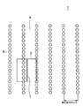
図1および図2はこの発明の第1の実施形態において用いるGaN基板1を示し、図1Aは斜視図、図1Bは領域Bの最近接方向の断面図、図2は平面図である。このGaN基板1はn型で(0001)面(C面)方位である。ただし、GaN基板1はR面、A面またはM面方位のものであってもよい。このGaN基板1においては、平均転位密度が低い結晶からなる領域Aの中に、平均転位密度が高い結晶からなる領域Bが六方格子状に周期的に配列している。ここで、領域Bは不定多角柱状の形状を有するのが一般的であるが、図1Aにおいては、簡略化して円柱形状としてある(以下同様)。この場合、最近接の領域B同士を結ぶ直線はGaNの〈1−100〉方向およびそれと等価な方向と一致している。ただし、最近接の領域B同士を結ぶ直線をGaNの〈11−20〉方向およびそれと等価な方向と一致するようにしてもよい。領域BはGaN基板1を貫通している。このGaN基板1の厚さは例えば200〜600μmである。なお、図2の破線は領域Bの相対的な位置関係を示すためのものにすぎず、実在する(物理的な意味のある)線ではない(以下同様)。
【0094】
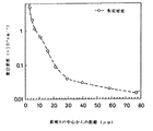
領域Bの配列周期(最近接の領域Bの中心同士の間隔)は例えば400μm、その直径は例えば20μmである。また、領域Aの平均転位密度は例えば2×106 cm-2、領域Bの平均転位密度は例えば1×108 cm-2である。領域Bの中心から半径方向の転位密度の分布の一例を図3に示す。
このGaN基板1は、結晶成長技術を用いて例えば次のようにして製造することができる。
このGaN基板1の製造に用いる基本的な結晶成長メカニズムは、ファセット面からなる斜面を有して成長させ、そのファセット面斜面を維持して成長させることで転位を伝播させ、所定の位置に集合させるものである。このファセット面により成長した領域は、転位の移動により、低密度の欠陥領域となる。そのファセット面斜面下部には、明確な境界を持った高密度の欠陥領域を有して成長が行われ、転位は、高密度の欠陥領域の境界あるいはその内部に集合し、ここで消滅あるいは蓄積する。
この高密度の欠陥領域の形状によって、ファセット面の形状も異なる。欠陥領域がドット状の場合は、そのドットを底として、ファセット面が取り巻き、ファセット面からなるピットを形成する。また、欠陥領域がストライプ状の場合は、ストライプを谷底として、その両側にファセット面斜面を有し、横に倒した三角形のプリズム状のファセット面となる。
その後、成長層の表面に研削、研磨を施すことにより、表面を平坦化し、基板として使用することができる形態とすることができる。
また、上記の高密度の欠陥領域は、いくつかの状態があり得る。例えば、多結晶からなる場合がある。また、単結晶であるが、周りの低密度欠陥領域に対して微傾斜している場合もある。また、周りの低密度欠陥領域に対して、C軸が反転している場合もある。こうして、この高密度欠陥領域は、明確な境界を有しており、周りと区別される。
この高密度欠陥領域を有して成長させることにより、その周りのファセット面を埋め込むことなく、ファセット面を維持して成長を進行することができる。
この高密度欠陥領域は、下地基板上にGaNを結晶成長させる際に、高密度欠陥領域を形成する場所に、種をあらかじめ形成しておくことにより、発生させることができる。その種としては、非晶質あるいは多結晶の層を形成する。その上から、GaNを成長させることで、ちょうどその種の領域に、高密度欠陥領域を形成することができる。
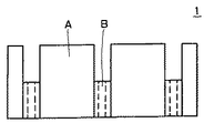
このGaN基板1の具体的な製造方法は次のとおりである。まず、下地基板を用意する。この下地基板としては種々の基板を用いることができ、一般的なサファイア基板でもよいが、後工程で除去することを考慮すると、除去しやすいGaAs基板などを用いることが好ましい。そして、この下地基板上に、例えばSiO2 膜からなる種を形成する。この種の形状は、例えばドット状またはストライプ状とすることができる。この種は規則正しく、多数個形成することができる。より具体的には、この場合、種は、図2に示す領域Bの配置に対応した配置で形成する。その後、例えばハイドライド気相エピタキシー(HVPE)により、GaNを厚膜成長させる。成長後、GaNの厚膜層の表面には、種のパターン形状に応じたファセット面が形成される。この第1の実施形態のように種がドット状のパターンの場合は、ファセット面からなるピットが規則正しく形成される。一方、種がストライプ状のパターンの場合は、プリズム状のファセット面が形成される。
その後、下地基板を除去し、さらにGaNの厚膜層を研削加工、研磨加工し、表面を平坦化する。これによって、GaN基板1を製造することができる。ここで、GaN基板1の厚さは、自由に設定することができる。
このようにして製造されたGaN基板1は、C面が主面であり、その中に、所定のサイズのドット状(あるいはストライプ状)の高密度欠陥領域、すなわち領域Bが規則正しく形成された基板となっている。領域B以外の単結晶領域、すなわち領域Aは、領域Bに比べて低転位密度となっている。
【0095】
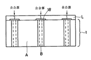
図4にこのGaN基板1の領域Bに存在する転位を破線で模式的に示す。このようなGaN基板1上に図5に示すようにGaN系半導体層Lを成長させると、このGaN系半導体層Lには下地のGaN基板1の領域Bから転位が伝播して品質が低下する。
【0096】
そこで、この第1の実施形態においては、図6に示すように、エッチングにより領域Bの上部を深さDだけ除去する。深さDは例えば1〜10μmとする。こうすることで、領域Bの表面を、GaN基板1の主面から十分に離すことができる。そして、図7に示すように、このGaN基板1上に、有機金属化学気相成長(MOCVD)法などにより素子構造を形成するGaN系半導体層Lを成長させる。このGaN系半導体層Lのうち領域Bの上に成長した部分には領域Bから転位が伝播するが、この転位が伝播する領域はごく一部に限定されるため、GaN基板1の主面上に成長したGaN系半導体層Lにその領域による悪影響が及ばないようにすることができる。
【0097】
領域Bのエッチングは次のようにして行うことができる。一般に、GaNなどの窒化物系III−V族化合物半導体は化学的に安定で、高温の、水酸化ナトリウムなどの強アルカリ、強塩酸やリン酸などの酸を除けば、室温付近でウエットエッチングは起こらない。しかしながら、GaN基板1において領域Bは領域Aに比べて転位密度、より一般的には欠陥密度がずっと高い。この欠陥密度が高い領域Bでは領域Aに比べて結晶を構成する原子の結合状態が不完全であり、完全結晶に近い領域Aよりもエッチング速度が速いため、領域Bを領域Aに対して選択的にエッチングすることができる。このエッチングは、領域Aの表面をレジストなどでマスクして行ってもよいが、GaN基板1を全面エッチングすることによっても領域Bだけを選択的にエッチングすることができる。エッチング速度を上げるために、エッチング液の温度を高くしてエッチングを行ってもよい。エッチング液は、例えば、アルカリ溶液としては水酸化カリウム(KOH)、酸としてはリン酸などを用いることができる。エッチング方法の具体例を挙げると、エッチング槽中に入れたKOH溶液を75℃に加熱保持し、その中にGaN基板1を10分間浸し、エッチング終了後GaN基板1を取り出し、純水洗浄を行い、乾燥窒素のブローにより乾燥を行う。このエッチングにより、領域Bを約5μmの深さまで除去することができる。ここで、このエッチング時にGaN基板1の裏面がエッチングされて面荒れなどが発生するのを防止する目的で、必要に応じて、GaN基板1の裏面に例えば厚さ20nmのTi膜と厚さ300nmのPt膜とを順次積層したTi/Pt膜を真空蒸着法などにより形成して保護膜とし、その後エッチングを行うようにしてもよい。なお、このTi/Pt膜は例えば王水によりエッチング除去することができる。
【0098】
領域Bのエッチングは上記のウエットエッチング以外に、例えば反応性イオンエッチング(RIE)のようなドライエッチングにより行ってもよく、水素雰囲気やアンモニア雰囲気などで800℃以上の温度で一定時間加熱保持することによる熱化学的エッチングにより行ってもよい。
【0099】
次に、図6に示すGaN基板1を用いたGaN系半導体レーザの具体的な製造プロセスの一例を説明する。ここでは、リッジ構造およびSCH(Separate Confinement Heterostructure)構造を有するGaN系半導体レーザについて説明する。
【0100】
すなわち、図8に示すように、まず、GaN基板1の表面をサーマルクリーニングなどにより清浄化した後、その上にMOCVD法により、n型GaNバッファ層5、n型AlGaNクラッド層6、n型GaN光導波層7、アンドープのGa1-x Inx N/Ga1-y Iny N多重量子井戸構造の活性層8、アンドープInGaN劣化防止層9、p型AlGaNキャップ層10、p型GaN光導波層11、p型AlGaNクラッド層12およびp型GaNコンタクト層13を順次エピタキシャル成長させる。
【0101】
ここで、n型GaNバッファ層5は厚さが例えば0.05μmであり、n型不純物として例えばSiがドープされている。n型AlGaNクラッド層6は厚さが例えば1.0μmであり、n型不純物として例えばSiがドープされ、Al組成は例えば0.08である。n型GaN光導波層7は厚さが例えば0.1μmであり、n型不純物として例えばSiがドープされている。アンドープInx Ga1-x N/Iny Ga1-y N多重量子井戸構造の活性層8は、例えば、井戸層としてのInx Ga1-x N層の厚さが3.5nmでx=0.14、障壁層としてのIny Ga1-y N層の厚さが7nmでy=0.02、井戸数が3である。
【0102】
アンドープInGaN劣化防止層9は、活性層8に接している面から、p型AlGaNキャップ層9に接している面に向かってIn組成が徐々に単調減少するグレーディッド構造を有し、活性層8に接している面におけるIn組成は活性層8の障壁層としてのIny Ga1-y N層のIn組成yと一致しており、p型AlGaNキャップ層10に接している面におけるIn組成は0となっている。このアンドープInGaN劣化防止層9の厚さは例えば20nmである。
【0103】
p型AlGaNキャップ層10は厚さが例えば10nmであり、p型不純物として例えばマグネシウム(Mg)がドープされている。このp型AlGaNキャップ層10のAl組成は例えば0.2である。このp型AlGaNキャップ層10は、p型GaN光導波層11、p型AlGaNクラッド層12およびp型GaNコンタクト層13の成長時に活性層8からInが脱離して劣化するのを防止するとともに、活性層8からのキャリア(電子)のオーバーフローを防止するためのものである。p型GaN光導波層11は厚さが例えば0.1μmであり、p型不純物として例えばMgがドープされている。p型AlGaNクラッド層12は厚さが例えば0.5μmであり、p型不純物として例えばMgがドープされ、Al組成は例えば0.08である。p型GaNコンタクト層13は厚さが例えば0.1μmであり、p型不純物として例えばMgがドープされている。
【0104】
また、Inを含まない層であるn型GaNバッファ層5、n型AlGaNクラッド層6、n型GaN光導波層7、p型AlGaNキャップ層10、p型GaN光導波層11、p型AlGaNクラッド層12およびp型GaNコンタクト層13の成長温度は例えば1000℃程度とし、Inを含む層であるGa1-x Inx N/Ga1-y Iny N多重量子井戸構造の活性層8の成長温度は例えば700〜800℃、例えば730℃とする。アンドープInGaN劣化防止層9の成長温度は、成長開始時点は活性層8の成長温度と同じく例えば730℃に設定し、その後例えば直線的に上昇させ、成長終了時点でp型AlGaNキャップ層10の成長温度と同じく例えば835℃になるようにする。
【0105】
これらのGaN系半導体層の成長原料は、例えば、Gaの原料としてはトリメチルガリウム((CH3 )3 Ga、TMG)、Alの原料としてはトリメチルアルミニウム((CH3 )3 Al、TMA)、Inの原料としてはトリメチルインジウム((CH3 )3 In、TMI)を、Nの原料としてはNH3 を用いる。また、キャリアガスとしては、例えば、H2 を用いる。ドーパントについては、n型ドーパントとしては例えばモノシラン(SiH4 )を、p型ドーパントとしては例えばビス=メチルシクロペンタジエニルマグネシウム((CH3 C5 H4 )2 Mg)あるいはビス=シクロペンタジエニルマグネシウム((C5 H5 )2 Mg)を用いる。
【0106】
次に、上述のようにしてGaN系半導体層を成長させたGaN基板1をMOCVD装置から取り出す。そして、p型GaNコンタクト層13の全面に例えばCVD法、真空蒸着法、スパッタリング法などにより例えば厚さが0.1μmのSiO2 膜(図示せず)を形成した後、このSiO2 膜上にリソグラフィーによりリッジ部の形状に対応した所定形状のレジストパターン(図示せず)を形成し、このレジストパターンをマスクとして、例えばフッ酸系のエッチング液を用いたウエットエッチング、または、CF4 やCHF3 などのフッ素を含むエッチングガスを用いたRIE法によりSiO2 膜をエッチングし、リッジ部に対応する形状とする。
【0107】
次に、このSiO2 膜をマスクとしてRIE法によりp型AlGaNクラッド層12の厚さ方向の所定の深さまでエッチングを行うことにより、図9に示すように、〈1−100〉方向に延在するリッジ14を形成する。このリッジ14の幅は例えば3μmである。このRIEのエッチングガスとしては例えば塩素系ガスを用いる。
【0108】
次に、エッチングマスクとして用いたSiO2 膜をエッチング除去した後、基板全面に例えばCVD法、真空蒸着法、スパッタリング法などにより例えば厚さが0.3μmのSiO2 膜のような絶縁膜15を成膜する。この絶縁膜15は電気絶縁および表面保護のためのものである。
【0109】
次に、リソグラフィーによりp側電極形成領域を除いた領域の絶縁膜15の表面を覆うレジストパターン(図示せず)を形成する。
次に、このレジストパターンをマスクとして絶縁膜15をエッチングすることにより、開口15aを形成する。
【0110】
次に、レジストパターンを残したままの状態で、基板全面に例えば真空蒸着法により例えばPd膜、Pt膜およびAu膜を順次形成した後、レジストパターンをその上に形成されたPd膜、Pt膜およびAu膜とともに除去する(リフトオフ)。これによって、絶縁膜15の開口15aを通じてp型GaNコンタクト層13にコンタクトしたp側電極16が形成される。ここで、このp側電極16を構成するPd膜、Pt膜およびAu膜の厚さは例えばそれぞれ10nm、100nmおよび300nmとする。次に、p側電極16をオーミック接触させるためのアロイ処理を行う。
【0111】
次に、GaN基板1の裏面に例えば真空蒸着法により例えばTi膜、Pt膜およびAu膜を順次形成し、Ti/Pt/Au構造のn側電極17を形成する。ここで、このn側電極17を構成するTi膜、Pt膜およびAu膜の厚さは例えばそれぞれ10nm、50nmおよび100nmとする。次に、n側電極17をオーミック接触させるためのアロイ処理を行う。
【0112】
次に、図10に示すように、素子領域2(太い実線で囲まれた一区画)の輪郭線に沿って、上述のようにしてレーザ構造が形成されたGaN基板1のスクライビングを劈開により行ってレーザバー4に加工して両共振器端面を形成する。次に、これらの共振器端面に端面コーティングを施した後、再びこのレーザバー4のスクライビングを劈開などにより行ってチップ化する。
【0113】
図10においては、グレーの長方形が一つのGaN系半導体レーザを表し、その中央付近に描かれた直線がレーザストライプ3であり、これが発光領域の位置に相当する。さらに、それらが連なった破線で描かれた長方形がレーザバー4を表していて、このレーザバー4の長辺が共振器端面に相当する。
【0114】
図10に示す例においては、GaN系半導体レーザのサイズが例えば600μm×346μmであり、横方向(長辺方向)は領域Bを結ぶ直線に沿って、縦方向(短辺方向)は領域Bを通らない直線に沿って、それぞれ基板のスクライビンを行うことによってそのサイズのGaN系半導体レーザに分離する。
【0115】
この場合、領域Bは各GaN系半導体レーザの長辺の端面部分にのみ存在することになるので、レーザストライプ3が短辺の中点同士を結ぶ直線の近傍に位置するように素子の設計を行うことにより、領域Bの影響が発光領域に及ぶことを避けることができる。
共振器のミラーについては、図10中の縦方向の直線に沿って、劈開などにより基板のスクライビングを行うことにより端面に形成されるが、その直線が領域Bを通らないので、領域Bにおける転位の影響を受けることはない。したがって、発光特性が良く、信頼性が高いGaN系半導体レーザを得ることができる。
以上により、図11に示すように、目的とするリッジ構造およびSCH構造を有するGaN系半導体レーザが製造される。
【0116】
以上のように、この第1の実施形態によれば、平均転位密度が低い領域Aの中に平均転位密度が高い領域Bが六方格子状に周期的に配列しているGaN基板1のうち領域Bの上部をエッチングにより除去して領域Bの表面をGaN基板1の主面から離した上で、このGaN基板1上にレーザ構造を形成するGaN系半導体層を成長させているので、レーザ構造の形成に使用されるGaN系半導体層に領域Bの悪影響が及ばないようにすることができる。このため、発光特性が良好で、信頼性が高く長寿命のGaN系半導体レーザを実現することができる。
【0117】
加えて、この第1の実施形態によれば、活性層8に接してアンドープInGaN劣化防止層9が設けられ、このアンドープInGaN劣化防止層9に接してp型AlGaNキャップ層10が設けられているので、アンドープInGaN劣化防止層9により、p型AlGaNキャップ層10により活性層8に発生する応力を大幅に緩和することができるとともに、p型層のp型ドーパントとして用いられるMgが活性層7に拡散するのを有効に抑制することができる。
【0118】
次に、この発明の第2の実施形態について説明する。
図12に示すように、この第2の実施形態においては、GaN基板1の領域Bの全部をエッチングにより除去し、その部分を完全に空洞化する。そして、図13に示すように、このGaN基板1上にMOCVD法などによりGaN系半導体層Lを成長させる。
上記以外のことは第1の実施形態と同様であるので、説明を省略する。
この第2の実施形態によっても、第1の実施形態と同様な利点を得ることができる。
【0119】
次に、この発明の第3の実施形態について説明する。
図14に示すように、この第3の実施形態においては、第1の実施形態と同様にGaN基板1の領域Bの上部をエッチング除去するが、この場合、このエッチングは例えばRIEなどのドライエッチングにより行う。この後、領域Bの結晶性が領域Aの結晶性より悪いことを利用して、領域A上では成長が起きるが、領域B上では成長が起きないような成長条件でMOCVD法などによりGaN系半導体層Lを成長させる。この結果、GaN基板1の主面、すなわち領域A上にのみGaN系半導体層Lが成長するようにすることができる。
上記以外のことは第1の実施形態と同様であるので、説明を省略する。
この第3の実施形態によっても、第1の実施形態と同様な利点を得ることができる。
【0120】
次に、この発明の第4の実施形態について説明する。
図15に示すように、この第4の実施形態においては、第1の実施形態と同様にGaN基板1の領域Bの上部をエッチング除去する。この後、領域Bの結晶性が領域Aの結晶性より悪いことを利用して、領域A上では成長が起きるが、領域B上では成長が起きないような成長条件でGaN系半導体層Lを横方向成長させる。この結果、GaN基板1の主面、すなわち領域A上からGaN系半導体層Lが横方向成長して領域Bの上方で会合し、最終的に表面を平坦化することができる。ただし、GaN系半導体層Lを会合させず、平坦化させないでもよい。
上記以外のことは第1の実施形態と同様であるので、説明を省略する。
この第4の実施形態によっても、第1の実施形態と同様な利点を得ることができる。
【0121】
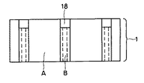
次に、この発明の第5の実施形態について説明する。
図16に示すように、この第5の実施形態においては、GaN基板1の主面のうち領域Bの部分を完全に覆うようにSiO2 膜などの絶縁膜18を形成する。この絶縁膜18は、領域Bを完全に覆うことができればどのような形状であってもよく、例えば、領域Bの形状に合わせて円形としても、領域Bを含む四角形その他の多角形としても、さらには一列に並んだ領域Bおよびその間の部分の領域Aを完全に覆うストライプ形状としてもよい。次に、図17に示すように、このGaN基板1上にMOCVD法などによりGaN系半導体層Lを成長させる。このとき、絶縁膜18が成長マスクの役割を果たすため、この絶縁膜18で覆われていない部分におけるGaN基板1の主面上にのみGaN系半導体層Lが成長する。
上記以外のことは第1の実施形態と同様であるので、説明を省略する。
この第5の実施形態によっても、第1の実施形態と同様な利点を得ることができる。
【0122】
次に、この発明の第6の実施形態について説明する。
図18に示すように、この第6の実施形態においては、第5の実施形態と同様に、GaN基板1の主面のうち領域Bの部分を完全に覆うようにSiO2 膜などの絶縁膜18を形成する。次に、図18および図19に示す過程を経て、GaN基板1上にMOCVD法などを用いてELOによりGaN系半導体層Lを横方向成長させる。このとき、絶縁膜18上で横方向成長するGaN系半導体層Lが会合する。ただし、GaN系半導体層Lを会合させないようにしてもよい。
上記以外のことは第1の実施形態と同様であるので、説明を省略する。
この第6の実施形態によっても、第1の実施形態と同様な利点を得ることができる。
【0123】
次に、この発明の第7の実施形態について説明する。
図20に示すように、この第7の実施形態においては、第1の実施形態と同様にGaN基板1の領域Bの上部をエッチング除去する。次に、GaN基板1の全面にSiO2 膜などの絶縁膜18を形成し、領域Bの除去部を埋める。次に、図21に示すように、例えばRIE法により絶縁膜18のエッチバックを行うことにより、領域Bの除去部にのみこの絶縁膜18を残す。この後、第5または第6の実施形態と同様に、GaN基板1上にGaN系半導体層Lを成長させる。
上記以外のことは第1の実施形態と同様であるので、説明を省略する。
この第7の実施形態によっても、第1の実施形態と同様な利点を得ることができる。
【0124】
次に、この発明の第8の実施形態について説明する。
図22に示すように、この第8の実施形態においては、第1の実施形態と同様にGaN基板1の領域Bの上部をエッチング除去する。次に、GaN基板1の全面にSiO2 膜などの絶縁膜18を形成する。このとき、この絶縁膜18の厚さが、領域Bの除去部が完全に埋められない程度に小さいとする。次に、例えばRIE法により絶縁膜18のエッチバックを行うことにより、領域A上の絶縁膜18を除去する。この後、第5または第6の実施形態と同様に、GaN基板1上にGaN系半導体層Lを成長させる。
上記以外のことは第1の実施形態と同様であるので、説明を省略する。
この第8の実施形態によっても、第1の実施形態と同様な利点を得ることができる。
【0125】
次に、この発明の第9の実施形態について説明する。
図23に示すように、この第9の実施形態においては、第1の実施形態と同様にGaN基板1の領域Bの上部をエッチング除去する。次に、GaN基板1の全面にSiO2 膜などの絶縁膜18を形成し、領域Bの除去部を埋めた後、この絶縁膜18をエッチングにより第5の実施形態と同様な形状にパターニングする。この後、第5または第6の実施形態と同様に、GaN基板1上にGaN系半導体層Lを成長させる。
上記以外のことは第1の実施形態と同様であるので、説明を省略する。
この第9の実施形態によっても、第1の実施形態と同様な利点を得ることができる。
【0126】
次に、この発明の第10の実施形態について説明する。
図24に示すように、この第10の実施形態においては、第1の実施形態と同様にGaN基板1の領域Bの上部をエッチング除去するが、この場合、エッチング深さは十分に大きく、例えば数十μm程度とする。次に、図25に示すように、GaN基板1の全面にSiO2 膜などの絶縁膜18形成する。このとき、領域Bの除去部が深いため、この除去部は絶縁膜18によって完全には埋められず、内部に空洞が形成されるとする。次に、例えばRIE法により絶縁膜18のエッチバックを行うことにより、領域A上の絶縁膜18を除去する。この後、第5または第6の実施形態と同様に、GaN基板1上にGaN系半導体層Lを成長させる。
上記以外のことは第1の実施形態と同様であるので、説明を省略する。
この第10の実施形態によっても、第1の実施形態と同様な利点を得ることができる。
【0127】
次に、この発明の第11の実施形態について説明する。
図27に示すように、この第11の実施形態においては、GaN基板1の領域Aの中に領域Bが六方格子状に周期的に配列していることは第1の実施形態と同様であるが、領域Aと領域Bとの間に、領域Aの平均転位密度と領域Bの平均転位密度との中間的な平均転位密度の領域Cが遷移領域として形成されていることが第1の実施形態と異なる。具体的には、領域Aの平均転位密度は2×106 cm-2以下、領域Bの平均転位密度は1×108 cm-2以上、領域Cの平均転位密度は1×108 cm-2より小さく、2×106 cm-2より大きく、例えば(1〜2)×107 cm-2程度である。領域Bの配列周期(最近接の領域Bの中心同士の間隔)は例えば300μm、その直径は例えば20μmである。また、領域Cの直径は例えば120μmである。
【0128】
この第11の実施形態においては、第1の実施形態においてはGaN基板1の領域Bの上部をエッチングにより除去したのに対し、GaN基板1の領域Bおよび領域Cの両方の上部をエッチングにより除去する。
上記以外のことは第1の実施形態と同様であるので、説明を省略する。
この第11の実施形態によっても、第1の実施形態と同様な利点を得ることができる。
【0129】
次に、この発明の第12の実施形態について説明する。
この第12の実施形態においては、第2の実施形態においてはGaN基板1の領域Bの全部をエッチングにより除去したのに対し、GaN基板1の領域Bおよび領域Cの両方の全部をエッチングにより除去する。
上記以外のことは第1および第11の実施形態と同様であるので、説明を省略する。
この第12の実施形態によっても、第1の実施形態と同様な利点を得ることができる。
【0130】
次に、この発明の第13の実施形態について説明する。
この第13の実施形態においては、第3の実施形態においてはGaN基板1の領域Bの上部をエッチングにより除去したのに対し、GaN基板1の領域Bおよび領域Cの両方の上部をエッチングにより除去する。
上記以外のことは第1および第11の実施形態と同様であるので、説明を省略する。
この第13の実施形態によっても、第1の実施形態と同様な利点を得ることができる。
【0131】
次に、この発明の第14の実施形態について説明する。
この第14の実施形態においては、第4の実施形態においてはGaN基板1の領域Bの上部をエッチングにより除去したのに対し、GaN基板1の領域Bおよび領域Cの両方の上部をエッチングにより除去する。
上記以外のことは第1および第11の実施形態と同様であるので、説明を省略する。
この第14の実施形態によっても、第1の実施形態と同様な利点を得ることができる。
【0132】
次に、この発明の第15の実施形態について説明する。
この第15の実施形態においては、第5の実施形態においてはGaN基板1の領域Bを絶縁膜18により覆ったのに対し、GaN基板1の領域Bおよび領域Cの両方を絶縁膜18により覆う。
上記以外のことは第1、第5および第11の実施形態と同様であるので、説明を省略する。
この第15の実施形態によっても、第1の実施形態と同様な利点を得ることができる。
【0133】
次に、この発明の第16の実施形態について説明する。
この第16の実施形態においては、第6の実施形態においてはGaN基板1の領域Bを絶縁膜18により覆ったのに対し、GaN基板1の領域Bおよび領域Cの両方を絶縁膜18により覆う。
上記以外のことは第1、第5および第11の実施形態と同様であるので、説明を省略する。
この第16の実施形態によっても、第1の実施形態と同様な利点を得ることができる。
【0134】
次に、この発明の第17の実施形態について説明する。
この第17の実施形態においては、第7の実施形態においてはGaN基板1の領域Bの上部をエッチングにより除去したのに対し、GaN基板1の領域Bおよび領域Cの両方の上部をエッチングにより除去する。
上記以外のことは第1、第5および第11の実施形態と同様であるので、説明を省略する。
この第17の実施形態によっても、第1の実施形態と同様な利点を得ることができる。
【0135】
次に、この発明の第18の実施形態について説明する。
この第18の実施形態においては、第8の実施形態においてはGaN基板1の領域Bの上部をエッチングにより除去したのに対し、GaN基板1の領域Bおよび領域Cの両方の上部をエッチングにより除去する。
上記以外のことは第1、第5および第11の実施形態と同様であるので、説明を省略する。
この第18の実施形態によっても、第1の実施形態と同様な利点を得ることができる。
【0136】
次に、この発明の第19の実施形態について説明する。
この第19の実施形態においては、第9の実施形態においてはGaN基板1の領域Bの上部をエッチングにより除去したのに対し、GaN基板1の領域Bおよび領域Cの両方の上部をエッチングにより除去する。
上記以外のことは第1、第5および第11の実施形態と同様であるので、説明を省略する。
この第19の実施形態によっても、第1の実施形態と同様な利点を得ることができる。
【0137】
次に、この発明の第20の実施形態について説明する。
この第20の実施形態においては、第10の実施形態においてはGaN基板1の領域Bの上部をエッチングにより除去したのに対し、GaN基板1の領域Bおよび領域Cの両方の上部をエッチングにより除去する。
上記以外のことは第1、第5および第11の実施形態と同様であるので、説明を省略する。
この第20の実施形態によっても、第1の実施形態と同様な利点を得ることができる。
【0138】
次に、この発明の第21の実施形態について説明する。
図28に示すように、この第21の実施形態においては、第1の実施形態と異なり、長方形の素子領域2の輪郭線は、その長辺および短辺とも、領域Bの中心同士を結ぶ直線からなる。この場合も、レーザストライプ3の位置は、素子領域2の短辺の中点同士を結ぶ線上とする。こうすることにより、領域Bの影響が発光領域に及ぶことを避けることができる。
【0139】
この第21の実施形態においては、領域Bの中心同士を結ぶ直線からなる、素子領域2の輪郭線に沿って劈開によりスクライビングを行うことにより共振器のミラーが形成されることが第1の実施形態と異なっている。
ここで、領域Bは転位が多いので、領域Aよりも壊れやすいと考えられる。したがって、領域B同士を結ぶ直線に沿ってスクライビングを行うと、領域Bがいわばミシン目のような役割を果たして領域Aの部分もきれいに劈開される。この際、領域Bの部分の端面は転位が多いため、必ずしも平坦にならないが、その間の領域Aの部分の端面は平坦となる。
【0140】
平坦性が必要とされるのは、レーザストライプ3の端面部分であるが、図28に示すような配置であれば、領域Bの部分の端面は発光特性などに悪影響を及ばさない。
上記以外のことは第1の実施形態と同様であるので、説明を省略する。
この第21の実施形態によっても、第1の実施形態と同様な利点を得ることができる。
【0141】
次に、この発明の第22の実施形態について説明する。
図29はこの第22の実施形態において用いるGaN基板を示す平面図である。図29に示すように、この第22の実施形態においては、領域Bがレーザストライプ3に含まれないように素子領域2が画定される。ここで、レーザストライプ3は領域Bから50μm以上離れている。この場合、素子領域2には2個の領域Bが含まれることになる。
上記以外のことは第1の実施形態と同様であるので、説明を省略する。
この第22の実施形態によれば、第1の実施形態と同様な利点を得ることができる。
【0142】
次に、この発明の第23の実施形態について説明する。
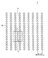
図30はこの第23の実施形態において用いるGaN基板を示す平面図である。このGaN基板1はn型でC面方位である。ただし、GaN基板1はR面、A面またはM面方位のものであってもよい。このGaN基板1においては、平均転位密度が低い結晶からなる領域Aの中に平均転位密度が高い結晶からなる領域BがGaNの〈11−20〉方向に例えば400μm間隔で周期的に配列し、〈11−20〉方向と直交する〈1−100〉方向に例えば20〜100μm間隔で周期的に配列している。ただし、〈11−20〉方向と〈1−100〉方向とを入れ替えてもよい。
【0143】
この第23の実施形態においては、図31に示すように、レーザストライプ3に平行な一対の端面が〈1−100〉方向の領域Bの列を通り、かつ、レーザストライプ3がこの領域Bの列の間の領域の中央付近に位置するように素子領域2が画定される。この場合、素子領域2には領域Bの列は実質的に含まれない。
上記以外のことは第1の実施形態と同様であるので、説明を省略する。
この第23の実施形態によれば、第1の実施形態と同様な利点を得ることができる。
【0144】
次に、この発明の第24の実施形態について説明する。
図32に示すように、この第24の実施形態においては、第23の実施形態と同様なGaN基板1を用いるが、レーザストライプ3に平行な一つの端面が〈1−100〉方向の領域Bの列を通り、他方の端面がこの領域Bの列から離れた位置を通る点で、第23の実施形態と異なる。この場合、素子領域2には領域Bの列は実質的に含まれない。
上記以外のことは第23および第1の実施形態と同様であるので、説明を省略する。
この第24の実施形態によれば、第1の実施形態と同様な利点を得ることができる。
【0145】
次に、この発明の第25の実施形態について説明する。
図33に示すように、この第25の実施形態においては、第23の実施形態と同様なGaN基板1を用いるが、レーザストライプ3に平行な一対の端面がいずれも〈1−100〉方向の領域Bの列の間に位置し、かつ、レーザストライプ3がこの領域Bの列の間の領域の中央付近に位置するように素子領域2が画定される点で、第23の実施形態と異なる。この場合、素子領域2には領域Bの列は実質的に含まれない。
上記以外のことは第23および第1の実施形態と同様であるので、説明を省略する。
この第25の実施形態によれば、第1の実施形態と同様な利点を得ることができる。
【0146】
次に、この発明の第26の実施形態について説明する。
図34に示すように、この第26の実施形態においては、第23の実施形態と同様なGaN基板1を用いるが、レーザストライプ3に平行な一つの端面が〈1−100〉方向の領域Bの列を通り、他方の端面がこの領域Bの列に直ぐ隣接する領域Bの列とその次の領域Bの列との間に位置し、かつ、レーザストライプ3が領域Bの列から50μm以上離れた位置を通る点で、第23の実施形態と異なる。この場合、素子領域2には領域Bの列は1本含まれる。
上記以外のことは第23および第1の実施形態と同様であるので、説明を省略する。
この第26の実施形態によれば、第1の実施形態と同様な利点を得ることができる。
【0147】
次に、この発明の第27の実施形態について説明する。
図35に示すように、この第27の実施形態においては、第23の実施形態と同様なGaN基板1を用いるが、レーザストライプ3に平行な一つの端面が〈1−100〉方向の領域Bの列から離れた位置を通り、他方の端面がこの領域Bの列に直ぐ隣接する領域Bの列とその次の領域Bの列との間に位置し、かつ、レーザストライプ3が領域Bの列から50μm以上離れた位置を通る点で、第23の実施形態と異なる。この場合、素子領域2には領域Bの列は1本含まれる。
上記以外のことは第23および第1の実施形態と同様であるので、説明を省略する。
この第27の実施形態によれば、第1の実施形態と同様な利点を得ることができる。
【0148】
次に、この発明の第28の実施形態について説明する。
図36はこの第28の実施形態において用いるGaN基板1を示す平面図である。このGaN基板1は、領域BがGaNの〈11−20〉方向に例えば200μm間隔で周期的に配列していることを除いて、第10の実施形態において用いたGaN基板1と同様である。この場合、素子領域2には領域Bの列は2本含まれる。
【0149】
図36に示すように、この第28の実施形態においては、レーザストライプ3が隣接する領域Bの列の間の領域の中央付近に位置し、かつ、レーザストライプ3に平行な一対の端面がこれらの領域Bの列とそれらの直ぐ外側の領域Bの列との間の領域の中央付近に位置する。
上記以外のことは第23および第1の実施形態と同様であるので、説明を省略する。
この第28の実施形態によれば、第1の実施形態と同様な利点を得ることができる。
【0150】
次に、この発明の第29の実施形態について説明する。
図37はこの第29の実施形態において用いるGaN基板を示す平面図である。このGaN基板1はn型でC面方位である。ただし、GaN基板1はR面、A面またはM面方位のものであってもよい。このGaN基板1においては、平均転位密度が低い結晶からなる領域Aの中に、平均転位密度が高い結晶からなり、GaNの〈1−100〉方向に線状に延在する領域Bが〈1−100〉方向と直交する〈11−20〉方向に例えば400μm間隔で周期的に配列している。ただし、〈1−100〉方向と〈11−20〉方向とを入れ替えてもよい。
【0151】
この第29の実施形態においては、図38に示すように、レーザストライプ3に平行な一対の端面が領域Bを通り、かつ、レーザストライプ3がこの領域Bの間の領域の中央付近に位置するように素子領域2が画定される。この場合、素子領域2には領域Bの列は実質的に含まれない。
上記以外のことは第1の実施形態と同様であるので、説明を省略する。
この第29の実施形態によれば、第1の実施形態と同様な利点を得ることができる。
【0152】
次に、この発明の第30の実施形態について説明する。
図39に示すように、この第30の実施形態においては、第29の実施形態と同様なGaN基板1を用いるが、レーザストライプ3に平行な一つの端面が領域Bを通り、他方の端面がこの領域Bの列から離れた位置を通る点で、第29の実施形態と異なる。この場合、素子領域2には領域Bの列は実質的に含まれない。上記以外のことは第29および第1の実施形態と同様であるので、説明を省略する。
この第30の実施形態によれば、第1の実施形態と同様な利点を得ることができる。
【0153】
次に、この発明の第31の実施形態について説明する。
図40に示すように、この第31の実施形態においては、第29の実施形態と同様なGaN基板1を用いるが、レーザストライプ3に平行な一対の端面がいずれも領域Bの間に位置し、かつ、レーザストライプ3がこの領域Bの間の領域の中央付近に位置するように素子領域2が画定される点で、第29の実施形態と異なる。この場合、素子領域2には領域Bの列は実質的に含まれない。
上記以外のことは第29および第1の実施形態と同様であるので、説明を省略する。
この第31の実施形態によれば、第1の実施形態と同様な利点を得ることができる。
【0154】
次に、この発明の第32の実施形態について説明する。
図41に示すように、この第32の実施形態においては、第29の実施形態と同様なGaN基板1を用いるが、レーザストライプ3に平行な一つの端面が領域Bを通り、他方の端面がこの領域Bの列に直ぐ隣接する領域Bとその次の領域Bとの間に位置し、かつ、レーザストライプ3が領域Bから50μm以上離れた位置を通る点で、第29の実施形態と異なる。この場合、素子領域2には領域Bは1本含まれる。
上記以外のことは第29および第1の実施形態と同様であるので、説明を省略する。
この第32の実施形態によれば、第1の実施形態と同様な利点を得ることができる。
【0155】
次に、この発明の第33の実施形態について説明する。
図42に示すように、この第33の実施形態においては、第29の実施形態と同様なGaN基板1を用いるが、レーザストライプ3に平行な一つの端面が領域Bから離れた位置を通り、他方の端面がこの領域Bに直ぐ隣接する領域Bとその次の領域Bとの間に位置し、かつ、レーザストライプ3が領域Bから50μm以上離れた位置を通る点で、第29の実施形態と異なる。この場合、素子領域2には領域Bの列は1本含まれる。
上記以外のことは第29および第1の実施形態と同様であるので、説明を省略する。
この第33の実施形態によれば、第1の実施形態と同様な利点を得ることができる。
【0156】
次に、この発明の第34の実施形態について説明する。
図43はこの第34の実施形態において用いるGaN基板1を示す平面図である。このGaN基板1は、領域BがGaNの〈11−20〉方向に例えば200μm間隔で周期的に配列していることを除いて、第29の実施形態において用いたGaN基板1と同様である。この場合、素子領域2には領域Bの列は2本含まれる。
【0157】
図43に示すように、この第34の実施形態においては、レーザストライプ3が隣接する領域Bの間の領域の中央付近に位置し、かつ、レーザストライプ3に平行な一対の端面がこれらの領域Bとそれらの直ぐ外側の領域Bとの間の領域の中央付近に位置する。
上記以外のことは第29および第1の実施形態と同様であるので、説明を省略する。
この第34の実施形態によれば、第1の実施形態と同様な利点を得ることができる。
【0158】
以上、この発明の実施形態について具体的に説明したが、この発明は、上述の実施形態に限定されるものではなく、この発明の技術的思想に基づく各種の変形が可能である。
【0159】
例えば、上述の実施形態において挙げた数値、構造、基板、原料、プロセスなどはあくまでも例に過ぎず、必要に応じて、これらと異なる数値、構造、基板、原料、プロセスなどを用いてもよい。
【0160】
具体的には、例えば、上述の実施形態においては、この発明をSCH構造のGaN系半導体レーザの製造に適用した場合について説明したが、この発明は、例えば、DH(Double Heterostructure)構造のGaN系半導体レーザの製造に適用してもよいことはもちろん、GaN系発光ダイオードの製造に適用してもよく、さらにはGaN系FETやGaN系ヘテロ接合バイポーラトランジスタ(HBT)などの窒化物系III−V族化合物半導体を用いた電子走行素子に適用してもよい。
【0161】
また、上述の実施形態において、GaN基板1がサファイア基板などの異種基板上に設けられたものであってもよい。
【0162】
また、上述の実施形態においては、GaN系半導体層の成長にMOCVD法を用いているが、GaN系半導体層の成長には、ハイドライド気相エピタキシャル成長またはハライド気相エピタキシャル成長(HVPE)や分子線エピタキシー(MBE)法などの他の成長方法を用いてもよい。
【0163】
さらに、上述の実施形態においては、MOCVD法により成長を行う際のキャリアガスとしてH2 ガスを用いているが、必要に応じて、他のキャリアガス、例えばH2 とN2 あるいはHe、Arガスなどとの混合ガスを用いてもよい。
また、上述の実施形態においては、劈開により共振器端面を形成しているが、共振器端面は例えばRIEのようなドライエッチングにより形成してもよい。
【0164】
【発明の効果】
以上説明したように、この発明によれば、発光素子構造あるいは素子構造を形成する窒化物系III−V族化合物半導体層、あるいは半導体層、あるいは各種の材料からなる層が、窒化物系III−V族化合物半導体基板、あるいは半導体基板、あるいは基板の主面上で、第1の領域より平均転位密度が高い、あるいは平均欠陥密度が高い、あるいは結晶性が悪い第2の領域と直接接触しないようにしているので、発光素子構造あるいは素子構造を形成する窒化物系III−V族化合物半導体層、あるいは半導体層、あるいは各種の材料からなる層に第2の領域による悪影響が及ばないようにすることができる。このため、発光特性などの特性が良好で信頼性も高く長寿命の半導体発光素子あるいは特性が良好で信頼性も高く長寿命の半導体素子あるいは特性が良好で信頼性も高く長寿命の各種の素子を実現することができる。
【図面の簡単な説明】
【図1】この発明の第1の実施形態において用いるGaN基板を示す斜視図および断面図である。
【図2】この発明の第1の実施形態において用いるGaN基板を示す平面図である。
【図3】この発明の第1の実施形態において用いるGaN基板の領域Bの近傍における転位密度の分布の一例を示す略線図である。
【図4】この発明の第1の実施形態との比較例を説明するための断面図である。
【図5】この発明の第1の実施形態との比較例を説明するための断面図である。
【図6】この発明の第1の実施形態において用いるGaN基板を示す断面図である。
【図7】この発明の第1の実施形態においてGaN基板上にGaN系半導体層を成長させた状態を示す断面図である。
【図8】この発明の第1の実施形態によるGaN系半導体レーザの製造方法を説明するための断面図である。
【図9】この発明の第1の実施形態によるGaN系半導体レーザの製造方法を説明するための断面図である。
【図10】この発明の第1の実施形態によるGaN系半導体レーザの製造方法を説明するための平面図である。
【図11】この発明の第1の実施形態によるGaN系半導体レーザの製造方法を説明するための断面図である。
【図12】この発明の第2の実施形態において用いるGaN基板を示す断面図である。
【図13】この発明の第2の実施形態においてGaN基板上にGaN系半導体層を成長させた状態を示す断面図である。
【図14】この発明の第3の実施形態においてGaN基板上にGaN系半導体層を成長させた状態を示す断面図である。
【図15】この発明の第4の実施形態においてGaN基板上にGaN系半導体層を成長させた状態を示す断面図である。
【図16】この発明の第5の実施形態において用いるGaN基板を示す断面図である。
【図17】この発明の第5の実施形態においてGaN基板上にGaN系半導体層を成長させた状態を示す断面図である。
【図18】この発明の第6の実施形態においてGaN基板上にGaN系半導体層を成長させた状態を示す断面図である。
【図19】この発明の第6の実施形態においてGaN基板上にGaN系半導体層を成長させた状態を示す断面図である。
【図20】この発明の第7の実施形態において用いるGaN基板の製造方法を説明するための断面図である。
【図21】この発明の第7の実施形態において用いるGaN基板の製造方法を説明するための断面図である。
【図22】この発明の第8の実施形態において用いるGaN基板を示す断面図である。
【図23】この発明の第9の実施形態において用いるGaN基板を示す断面図である。
【図24】この発明の第10の実施形態において用いるGaN基板の製造方法を説明するための断面図である。
【図25】この発明の第10の実施形態において用いるGaN基板の製造方法を説明するための断面図である。
【図26】この発明の第10の実施形態において用いるGaN基板の製造方法を説明するための断面図である。
【図27】この発明の第11の実施形態において用いるGaN基板を示す平面図である。
【図28】この発明の第21の実施形態によるGaN系半導体レーザの製造方法を説明するための平面図である。
【図29】この発明の第22の実施形態によるGaN系半導体レーザの製造方法を説明するための平面図である。
【図30】この発明の第23の実施形態によるGaN系半導体レーザの製造方法を説明するための平面図である。
【図31】この発明の第23の実施形態によるGaN系半導体レーザの製造方法を説明するための平面図である。
【図32】この発明の第24の実施形態によるGaN系半導体レーザの製造方法を説明するための平面図である。
【図33】この発明の第25の実施形態によるGaN系半導体レーザの製造方法を説明するための平面図である。
【図34】この発明の第26の実施形態によるGaN系半導体レーザの製造方法を説明するための平面図である。
【図35】この発明の第27の実施形態によるGaN系半導体レーザの製造方法を説明するための平面図である。
【図36】この発明の第28の実施形態によるGaN系半導体レーザの製造方法を説明するための平面図である。
【図37】この発明の第29の実施形態によるGaN系半導体レーザの製造方法を説明するための平面図である。
【図38】この発明の第29の実施形態によるGaN系半導体レーザの製造方法を説明するための平面図である。
【図39】この発明の第30の実施形態によるGaN系半導体レーザの製造方法を説明するための平面図である。
【図40】この発明の第31の実施形態によるGaN系半導体レーザの製造方法を説明するための平面図である。
【図41】この発明の第32の実施形態によるGaN系半導体レーザの製造方法を説明するための平面図である。
【図42】この発明の第33の実施形態によるGaN系半導体レーザの製造方法を説明するための平面図である。
【図43】この発明の第34の実施形態によるGaN系半導体レーザの製造方法を説明するための平面図である。
【符号の説明】
1・・・GaN基板、2・・・素子領域、3・・・レーザストライプ、5・・・n型GaNバッファ層、6・・・n型AlGaNクラッド層、7・・・n型GaN光導波層、8・・・活性層、9・・・アンドープInGaN劣化防止層、10・・・p型AlGaNキャップ層、11・・・p型GaN光導波層、12・・・p型AlGaNクラッド層、13・・・p型GaNコンタクト層、14・・・リッジ、15、18・・・絶縁膜、16・・・n側電極、17・・・p側電極[0001]
BACKGROUND OF THE INVENTION
This invention relates to the manufacture of semiconductor light emitting devices. Method For example, the present invention is suitable for manufacturing a semiconductor laser, a light emitting diode, or an electron transit device using a nitride III-V compound semiconductor.
[0002]
[Prior art]
Nitride III-V compound semiconductors such as GaN, AlGaN, GaInN, and AlGaInN have a band gap E as compared with AlGaInAs III-V compound semiconductors and AlGaInP III-V compound semiconductors. g And is a direct transition semiconductor material. For this reason, these nitride III-V compound semiconductors are semiconductor lasers capable of emitting short-wavelength light from ultraviolet to green, and light-emitting diodes that can cover a wide emission wavelength range from ultraviolet to red and white (LED) has attracted attention as a material constituting semiconductor light emitting devices such as (LED), and is widely considered for applications such as high-density optical discs, full-color displays, and environmental / medical fields.
[0003]
Further, these nitride III-V compound semiconductors have a high saturation rate in a high electric field of GaN, for example, can operate at a high temperature up to about 400 ° C., and, for example, MIS (Metal-Insulator- Using AlN as the material of the insulating layer in the (Semiconductor) structure, the semiconductor layer and the insulating layer can be continuously formed by crystal growth. For this reason, these nitride III-V compound semiconductors are also expected as materials constituting high-power high-frequency electronic devices that can operate at high temperatures.
[0004]
In addition, the following can be cited as the advantages of the nitride III-V compound semiconductor.
(1) The thermal conductivity is higher than that of GaAs-based semiconductors and the like, and it is suitable for high temperature and high output operation devices.
(2) The material is chemically stable, has high hardness, and easily obtains high reliability.
(3) It is a compound semiconductor material with a low environmental load. That is, the AlGaInN-based semiconductor does not contain environmental pollutants and poisons that have a large environmental impact in the constituent materials and raw materials. Specifically, a material corresponding to arsenic (As) in an AlGaAs-based semiconductor, cadmium (Cd) in a ZnCdSSe-based semiconductor, and a raw material (arsine (AsH Three )) Etc. are not used.
[0005]
However, conventionally, a device using a nitride III-V compound semiconductor has a problem that there is no appropriate substrate material for obtaining high reliability.
In order to obtain a particularly high-quality crystal as a substrate material for a nitride III-V compound semiconductor, there are the following problems and situations.
(1) The constituent materials GaN, AlGaN, and GaInN are all strain systems having different lattice constants. Therefore, there are design limitations such as suppressing the composition and thickness in a range where no cracks or the like are generated between the nitride-based III-V compound semiconductors and the substrate and a range where a high-quality crystal film is obtained. .
(2) A high quality substrate that lattice matches with GaN has not yet been developed. For example, high-quality GaN substrates are under development, such as high-quality GaAs substrates lattice-matched to GaAs-based semiconductors and GaInP-based semiconductors, and high-quality InP substrates lattice-matched to GaInAs-based semiconductors. A small SiC substrate is expensive, difficult to increase in diameter, and has a problem that a tensile strain is generated in the crystal film, so that a crack is likely to occur. There is no.
(3) As a necessary condition for a substrate material of a nitride III-V compound semiconductor, it may not be altered or corroded at a high crystal growth temperature of about 1000 ° C. and an ammonia atmosphere of a Group V raw material.
[0006]
For the reasons described above, a sapphire substrate is often used as a nitride-based III-V group compound semiconductor substrate by comprehensive judgment.
The sapphire substrate is stable at the crystal growth temperature of the nitride-based III-V compound semiconductor, and has an advantage that a high-
[0007]
In addition to this, since the sapphire substrate has (1) no cleaving property, it is difficult to stably form a laser end face with high specularity. (2) Since sapphire is insulative, the p-side electrode and the n-side electrode are separated from the top surface of the substrate. Removal is essential. (3) If the crystal growth film is thick, the substrate warpage at room temperature is large due to the difference in thermal expansion coefficient between the nitride III-V compound semiconductor and sapphire, which hinders the device formation process. There is a problem such as.
[0008]
In order to improve the quality of a semiconductor crystal grown on a substrate having a different lattice constant such as a sapphire substrate, there is a method using lateral selective overgrowth (ELO). In ELO, a high crystal quality region (lateral growth region) and a low crystal quality or high defect density region (on the seed crystal, its boundary, an association portion, etc.) periodically appear, but the active region of the device (for example, light emission) If the size of the light emitting region in the device and the region in which the electron travels in the electron traveling device) is not large, the period of ELO is larger than the semiconductor laser stripe or the emitter / collector region (or source region / drain region) spacing of the transistor. Can take. For example, since the size of the active region of the element is about several μm for an ELO period of 10 to 20 μm, the active region can be designed in a high quality region.
[0009]
In the case where an element is formed on the sapphire substrate using ELO, there are the following problems in addition to the problems caused by the properties of sapphire itself such as the above-mentioned poor cleavage property.
(1) Since the number of steps required for ELO is large, the yield decreases.
(2) The crystal film thickness increases by an amount necessary for ELO, so that the substrate is greatly warped due to thermal stress, and the controllability of the crystal growth process and the wafer process is lowered. (3) There is a limit on the element size. In an element having an active region longer than the ELO cycle, for example, several hundred μm square or more, such as an LED, a photodetector (PD), and an integrated device, the entire device region cannot be made a high crystal quality region, so that the effect of ELO is exhibited. Can not.
[0010]
The above problems can be solved if a high-quality GaN substrate is obtained, but high-quality and large-diameter GaN substrates have not been obtained so far. This is because GaN cannot stably perform single crystal growth because HVPE (halide vapor phase growth) generally makes it difficult to obtain a high-quality seed crystal by high-temperature (high-pressure) growth. Due to the difficulty of manufacturing.
[0011]
Japanese Patent Application Laid-Open No. 2001-102307 proposes a method of manufacturing a single crystal GaN substrate for the purpose of improving this problem. According to this, after forming a GaN seed substrate having a high defect density, a three-dimensional facet (hereinafter referred to as “core”) is formed in part, and the growth is continued under the condition that the facet is not closed. Crystal dislocations are concentrated on the part, and as a result, a high quality substrate is manufactured in a wide area.
[0012]
[Problems to be solved by the invention]
However, since the technique disclosed in Japanese Patent Laid-Open No. 2001-102307 reduces threading dislocations in other regions by concentrating threading dislocations in a region where a growth layer is present, the obtained single crystal In the GaN substrate, a low defect density region (core) and a high defect density region are mixed, and the position where the high defect density region is generated cannot be controlled and is generated randomly. For this reason, when a semiconductor device such as a semiconductor laser is manufactured by growing a nitride III-V compound semiconductor layer on this single crystal GaN substrate, a high defect density region is formed in the light emitting region. Inevitably, the emission characteristics and reliability of the semiconductor laser are reduced.
[0013]
Accordingly, the problem to be solved by the present invention is to manufacture a semiconductor light emitting device having good characteristics such as light emission characteristics, high reliability and long life, and manufacturing a semiconductor light emitting device capable of easily manufacturing such a semiconductor light emitting device It is to provide a method.
[0014]
More generally, the problem to be solved by the present invention is to provide a semiconductor device having good characteristics, high reliability and long life, and a method of manufacturing a semiconductor device capable of easily manufacturing such a semiconductor device There is to do.
[0015]
More generally, the problem to be solved by the present invention is to provide various elements having good characteristics, high reliability and long life, and an element manufacturing method capable of easily manufacturing such elements. There is.
[0016]
In addition, the problem to be solved by the present invention is that a semiconductor light emitting device having good characteristics such as light emission characteristics and high reliability and a long life or a good characteristics and reliability and a semiconductor device or characteristics having a long life and good characteristics are reliable. It is an object of the present invention to provide a nitride III-V compound semiconductor layer growth method, a semiconductor layer growth method, and a layer growth method that are suitable for use in the manufacture of various types of devices having high properties and long lifetimes.
[0017]
[Means for Solving the Problems]
The present inventor has intensively studied to solve the above problems. The outline is as follows.
[0018]
The present inventor has succeeded in controlling the position of the high defect density region generated in the low defect density region as a result of improving the technique disclosed in Japanese Patent Application Laid-Open No. 2001-102307. That is, instead of naturally agglomerating and forming a high defect density region during crystal growth, a seed crystal or the like is artificially formed on a suitable substrate such as a GaAs substrate regularly, for example, periodically, for example, periodically. Further, by performing crystal growth thereon, the formation position of the high defect density region can be controlled, and the crystal quality can be improved and the high quality crystal region can be expanded. In this case, the arrangement pattern of the high defect density region can be freely changed by arranging the seed crystal or the like.
[0019]
Here, the seed crystal or the like is, for example, polycrystalline, amorphous (single crystal) or single crystal GaN, nitride-based III-V compound semiconductor other than GaN such as AlGaInN, or nitride-based III-V group. Although it is formed of a material other than a compound semiconductor, any structure may be used as long as it is a structure that serves as a nucleus that defines a crystal defect concentration position.
[0020]
When a semiconductor light emitting device such as a semiconductor laser, more generally a semiconductor device, is manufactured using such a substrate, it is necessary to eliminate the adverse effect of the high defect density region existing on the substrate on the device. That is, when a semiconductor layer is grown on a substrate, defects are propagated from the high defect density region of the base substrate to the semiconductor layer. Therefore, it is necessary to prevent deterioration of element characteristics and reliability due to the defect. There is.
[0021]
This problem also occurs when it is difficult to obtain a substrate having the same quality and low defect density as the semiconductor used for the device, and when a semiconductor layer is grown on the same structure as described above. is there. More generally, when it is difficult to obtain a substrate having the same quality and low defect density as the material used for the device, this also occurs when a layer having the same structure as described above is used to grow a layer thereon. It is.
As a result of various studies, the present inventor has found an effective technique capable of solving the above-described problems and has come up with the present invention.
[0022]
That is, in order to solve the above problem, the first invention of the present invention is:
A nitride system in which a plurality of second regions having a second average dislocation density higher than the first average dislocation density are regularly arranged in a first region made of a crystal having a first average dislocation density. A method of manufacturing a semiconductor light emitting device, wherein a semiconductor light emitting device is manufactured by growing a nitride III-V compound semiconductor layer forming a light emitting device structure on a main surface of a III-V compound semiconductor substrate. And
The nitride-based III-V compound semiconductor layer is prevented from being in direct contact with the second region on the main surface of the nitride-based III-V compound semiconductor substrate.
It is characterized by this.
[0023]
In order to prevent the nitride-based III-V compound semiconductor layer from coming into direct contact with the second region on the main surface of the nitride-based III-V compound semiconductor substrate, specifically, for example, nitride The second region is at least partially removed from the main surface of the nitride III-V compound semiconductor substrate before growing the III-V compound semiconductor layer. More specifically, before growing the nitride III-V compound semiconductor layer, the second region is removed from the main surface of the nitride III-V compound semiconductor substrate to a predetermined depth. Here, the predetermined depth is appropriately selected according to the configuration of the element constituted by the nitride III-V compound semiconductor layer, the growth condition of the nitride III-V compound semiconductor layer, etc. Specifically, the thickness is set to 1 μm or more, preferably about the thickness of the element formed using the nitride III-V compound semiconductor layer (for example, 10 μm or more). The entire second region may be removed before growing the nitride III-V compound semiconductor layer. The removal of the second region is typically performed by etching, specifically, wet etching, dry etching, thermochemical etching, ion milling, or the like.
[0024]
In order to prevent the nitride III-V compound semiconductor layer from coming into direct contact with the second region on the main surface of the nitride III-V compound semiconductor substrate, the nitride III-V compound semiconductor The surface of the second region may be covered with a covering layer before the layer is grown. Various coatings can be used as long as they can withstand the growth temperature. 2 Film, Si x N y In addition to insulating films such as films and SOG (Spin on Glass) films, refractory metal films such as tungsten (W), molybdenum (Mo), and tantalum (Ta), and nitride films thereof can be used. In this case, a coating layer may be simply formed on the second region, but when the second region is removed from the main surface of the nitride-based III-V compound semiconductor substrate to a predetermined depth. The portion from which the second region is removed may be filled with the coating layer. In the former case, the surface of the coating layer is located higher than the main surface of the nitride-based III-V compound semiconductor substrate. In the latter case, the surface of the coating layer can be obtained by using an etch-back technique. Can coincide with the main surface of the nitride III-V compound semiconductor substrate.
[0025]
The interval between two adjacent second regions or the arrangement period of the second regions is selected according to the size of the element, etc., but is generally 20 μm or more, 50 μm or more, or 100 μm or more. The upper limit of the interval between the second regions or the arrangement period of the second regions is not necessarily clear, but is generally about 1000 μm. This second region typically penetrates the nitride III-V compound semiconductor substrate. The second region typically has an indefinite polygonal column shape. A third region having a third average dislocation density higher than the first average dislocation density and lower than the second average dislocation density exists as a transition region between the first region and the second region. In this case, the nitride-based III-V compound semiconductor layer may not be in direct contact with the second region on the main surface of the nitride-based III-V compound semiconductor substrate. Most preferably, the nitride-based III-V compound semiconductor layer is not in direct contact with these second and third regions on the main surface of the nitride-based III-V compound semiconductor substrate. In the latter case, specifically, for example, before the nitride-based III-V compound semiconductor layer is grown, the second region and the third region are separated from the main surface of the nitride-based III-V compound semiconductor substrate. Remove at least part of it.
[0026]
The diameter of the second region is typically 10 μm or more and 100 μm or less, and more typically 20 μm or more and 50 μm or less. When the third region is present, the diameter thereof is typically greater than or equal to 20 μm and less than or equal to 200 μm, more typically greater than or equal to 40 μm and less than or equal to 160 μm, and most typically greater than or equal to 60 μm. Larger than 140 μm.
[0027]
The average dislocation density in the second region is generally at least 5 times the dislocation density in the first region. Typically, the average dislocation density in the first region is 2 × 10 6 cm -2 Hereinafter, the average dislocation density in the second region is 1 × 10. 8 cm -2 That's it. When the third region is present, its average dislocation density is typically 1 × 10 8 cm -2 Smaller 2 × 10 6 cm -2 Greater than.
[0028]
The light emitting region of the semiconductor light emitting element is separated from the second region by 1 μm or more, preferably 10 μm or more, more preferably 100 μm or more in order to prevent adverse effects due to the second region having a high average dislocation density. When the third region exists, it is most preferable that the light emitting region of the semiconductor light emitting element does not include the second region and the third region. More specifically, the semiconductor light emitting element is a semiconductor laser or a light emitting diode. However, in the case of the former semiconductor laser, the region where the drive current flows through the stripe electrode is preferably 1 μm or more from the second region, More preferably, it is 10 μm or more, and more preferably 100 μm or more. When the third region exists, it is most preferable that the region through which the driving current flows through the stripe electrode does not include the second region and the third region. One or a plurality of stripe-shaped electrodes, that is, laser stripes may be provided, and the width thereof may be selected as necessary.
[0029]
A nitride III-V compound semiconductor substrate or a nitride III-V compound semiconductor layer is most commonly Al. X B y Ga 1-xyz In z As u N 1-uv P v (However, 0 ≦ x ≦ 1, 0 ≦ y ≦ 1, 0 ≦ z ≦ 1, 0 ≦ u ≦ 1, 0 ≦ v ≦ 1, 0 ≦ x + y + z <1, 0 ≦ u + v <1), more specifically Al X B y Ga 1-xyz In z N (where 0 ≦ x ≦ 1, 0 ≦ y ≦ 1, 0 ≦ z ≦ 1, 0 ≦ x + y + z <1), typically Al X Ga 1-xz In z N (however, 0 ≦ x ≦ 1, 0 ≦ z ≦ 1). The nitride-based III-V compound semiconductor substrate is most typically made of GaN.
What has been described in relation to the first invention of the present invention is also valid for the following inventions as long as it is not contrary to the nature thereof.
[0030]
The second invention of this invention is:
A nitride system in which a plurality of second regions having a second average defect density higher than the first average defect density are regularly arranged in a first region made of a crystal having a first average defect density. A method of manufacturing a semiconductor light emitting device, wherein a semiconductor light emitting device is manufactured by growing a nitride III-V compound semiconductor layer forming a light emitting device structure on a main surface of a III-V compound semiconductor substrate. And
The nitride-based III-V compound semiconductor layer is prevented from being in direct contact with the second region on the main surface of the nitride-based III-V compound semiconductor substrate.
It is characterized by this.
[0031]
Here, the “average defect density” means the average density of the entire lattice defects that adversely affect the characteristics and reliability of the device, and the defects include all sorts of dislocations, stacking faults, point defects, etc. The same).
[0032]
The third invention of the present invention is:
A light emitting device on a main surface of a nitride III-V compound semiconductor substrate in which a plurality of second regions having lower crystallinity than the first region are regularly arranged in the first region made of crystal A method of manufacturing a semiconductor light-emitting device by growing a nitride-based III-V compound semiconductor layer that forms a structure, wherein the nitride-based III-V compound semiconductor layer is nitrided Preventing direct contact with the second region on the main surface of the physical group III-V compound semiconductor substrate
It is characterized by this.
[0033]
Here, typically, the first region made of a crystal is a single crystal, and the second region having lower crystallinity than the first region is a single crystal, polycrystal, amorphous, or two or more thereof. Are mixed (the same applies hereinafter). This corresponds to the case where the average dislocation density or average defect density in the second region is higher than the average dislocation density or average defect density in the first region.
[0034]
The fourth invention of the present invention is:
A nitride system in which a plurality of second regions having a second average dislocation density higher than the first average dislocation density are regularly arranged in a first region made of a crystal having a first average dislocation density. A method for manufacturing a semiconductor device, wherein a semiconductor device is manufactured by growing a nitride III-V compound semiconductor layer forming an element structure on a main surface of a group III-V compound semiconductor substrate,
The nitride-based III-V compound semiconductor layer is prevented from being in direct contact with the second region on the main surface of the nitride-based III-V compound semiconductor substrate.
It is characterized by this.
[0035]
The fifth invention of the present invention is:
A nitride system in which a plurality of second regions having a second average defect density higher than the first average defect density are regularly arranged in a first region made of a crystal having a first average defect density. A method for manufacturing a semiconductor device, wherein a semiconductor device is manufactured by growing a nitride III-V compound semiconductor layer forming an element structure on a main surface of a group III-V compound semiconductor substrate,
The nitride-based III-V compound semiconductor layer is prevented from being in direct contact with the second region on the main surface of the nitride-based III-V compound semiconductor substrate.
It is characterized by this.
[0036]
The sixth invention of the present invention is:
An element structure on a main surface of a nitride III-V compound semiconductor substrate in which a plurality of second regions having lower crystallinity than the first region are regularly arranged in the first region made of crystal A method for manufacturing a semiconductor device, wherein a semiconductor device is manufactured by growing a nitride III-V compound semiconductor layer forming
The nitride-based III-V compound semiconductor layer is prevented from being in direct contact with the second region on the main surface of the nitride-based III-V compound semiconductor substrate.
It is characterized by this.
[0037]
In the fourth to sixth aspects of the present invention, the semiconductor element includes a light emitting element such as a light emitting diode and a semiconductor laser, a light receiving element, a field effect transistor (FET) such as a high electron mobility transistor, and a heterogeneous element. An electron transit device such as a junction bipolar transistor (HBT) is included (the same applies hereinafter).
[0038]
In the fourth to sixth inventions of the present invention, the active region of the semiconductor element is preferably 1 μm or more, more preferably from the second region in order to prevent adverse effects due to the second region having a high average dislocation density. Is 10 μm or more, more preferably 100 μm or more. When the third region exists, it is most preferable that the active region of the semiconductor element does not include the second region and the third region. Here, the active region means a light emitting region in a semiconductor light emitting device, a light receiving region in a semiconductor light receiving device, and a region in which electrons travel in an electron traveling device (the same applies hereinafter).
[0039]
The seventh invention of the present invention is:
A semiconductor substrate in which a plurality of second regions having a second average dislocation density higher than the first average dislocation density are regularly arranged in a first region made of a crystal having a first average dislocation density. A method of manufacturing a semiconductor light emitting device, wherein a semiconductor light emitting device is manufactured by growing a semiconductor layer forming a light emitting device structure on a main surface,
The semiconductor layer should not be in direct contact with the second region on the main surface of the semiconductor substrate.
It is characterized by this.
[0040]
The eighth invention of the present invention is:
A semiconductor substrate in which a plurality of second regions having a second average defect density higher than the first average defect density are regularly arranged in a first region made of a crystal having a first average defect density. A method of manufacturing a semiconductor light emitting device, wherein a semiconductor light emitting device is manufactured by growing a semiconductor layer forming a light emitting device structure on a main surface,
The semiconductor layer should not be in direct contact with the second region on the main surface of the semiconductor substrate.
It is characterized by this.
[0041]
The ninth aspect of the present invention is:
A semiconductor layer for forming a light emitting element structure is grown on a main surface of a semiconductor substrate in which a plurality of second regions having lower crystallinity than the first region are regularly arranged in the first region made of crystal A method for manufacturing a semiconductor light emitting device, wherein the semiconductor light emitting device is manufactured by:
The semiconductor layer should not be in direct contact with the second region on the main surface of the semiconductor substrate.
It is characterized by this.
[0042]
The tenth aspect of the present invention is:
A semiconductor substrate in which a plurality of second regions having a second average dislocation density higher than the first average dislocation density are regularly arranged in a first region made of a crystal having a first average dislocation density. A method of manufacturing a semiconductor element, wherein a semiconductor element is manufactured by growing a semiconductor layer forming an element structure on a main surface,
The semiconductor layer should not be in direct contact with the second region on the main surface of the semiconductor substrate.
It is characterized by this.
[0043]
The eleventh aspect of the present invention is:
A semiconductor substrate in which a plurality of second regions having a second average defect density higher than the first average defect density are regularly arranged in a first region made of a crystal having a first average defect density. A method of manufacturing a semiconductor element, wherein a semiconductor element is manufactured by growing a semiconductor layer forming an element structure on a main surface,
The semiconductor layer should not be in direct contact with the second region on the main surface of the semiconductor substrate.
It is characterized by this.
[0044]
The twelfth aspect of the present invention is
A semiconductor layer forming an element structure is grown on a main surface of a semiconductor substrate in which a plurality of second regions having lower crystallinity than the first region are regularly arranged in the first region made of crystals. A method for manufacturing a semiconductor element by manufacturing a semiconductor element,
The semiconductor layer should not be in direct contact with the second region on the main surface of the semiconductor substrate.
It is characterized by this.
[0045]
In the tenth to twelfth inventions of the present invention, the material of the semiconductor substrate or semiconductor layer may be a nitride III-V compound semiconductor, a wurtzit structure, or more generally a hexagonal crystal system. Other semiconductors having a crystal structure, such as ZnO, α-ZnS, α-CdS, α-CdSe, and the like, and various semiconductors having other crystal structures may be used.
[0046]
The thirteenth invention of the present invention is
A main substrate in which a plurality of second regions having a second average dislocation density higher than the first average dislocation density are regularly arranged in a first region made of a crystal having a first average dislocation density. A device manufacturing method for manufacturing a device by growing a layer forming a device structure on a surface,
The layer should not be in direct contact with the second area on the main surface of the substrate
It is characterized by this.
[0047]
The fourteenth aspect of the present invention is:
A main substrate in which a plurality of second regions having a second average defect density higher than the first average defect density are regularly arranged in a first region made of a crystal having a first average defect density. A device manufacturing method for manufacturing a device by growing a layer forming a device structure on a surface,
The layer should not be in direct contact with the second area on the main surface of the substrate
It is characterized by this.
[0048]
The fifteenth aspect of the present invention is:
By growing a layer forming an element structure on the main surface of the substrate in which a plurality of second regions having lower crystallinity than the first region are regularly arranged in the first region made of crystals An element manufacturing method for manufacturing an element,
The layer should not be in direct contact with the second area on the main surface of the substrate
It is characterized by this.
[0049]
In the thirteenth to fifteenth aspects of the present invention, the element is a semiconductor element (light emitting element, light receiving element, electron transit element, etc.), piezoelectric element, pyroelectric element, optical element (secondary using a nonlinear optical crystal). Harmonic generation elements), dielectric elements (including ferroelectric elements), superconducting elements, and the like. In this case, as the material of the substrate or layer, various semiconductors as described above can be used in the semiconductor element, and in the piezoelectric element, pyroelectric element, optical element, dielectric element, superconducting element, etc., for example, oxide Various materials can be used. There are many oxide materials such as those disclosed in Journal of the Society of Japan Vol. 103, No. 11 (1995) pp. 1099-1111 and Materials Science and Engineering B41 (1996) 166-173. There is.
[0050]
The sixteenth invention of the present invention is
A plurality of second regions having a second average dislocation density higher than the first average dislocation density in the first region made of a crystal having the first average dislocation density at a first interval in the first direction. On the main surface of the nitride-based III-V group compound semiconductor substrate regularly arranged and regularly arranged in a second direction orthogonal to the first direction at a second interval smaller than the first interval A method for manufacturing a semiconductor light emitting device, wherein a semiconductor light emitting device is manufactured by growing a nitride III-V compound semiconductor layer forming a light emitting device structure on the substrate,
The nitride-based III-V compound semiconductor layer is prevented from being in direct contact with the second region on the main surface of the nitride-based III-V compound semiconductor substrate.
It is characterized by this.
[0051]
The seventeenth aspect of the present invention is:
A plurality of second regions having a second average defect density higher than the first average defect density in the first region made of a crystal having the first average defect density at a first interval in the first direction. On the main surface of the nitride-based III-V group compound semiconductor substrate regularly arranged and regularly arranged in a second direction orthogonal to the first direction at a second interval smaller than the first interval A method for manufacturing a semiconductor light emitting device, wherein a semiconductor light emitting device is manufactured by growing a nitride III-V compound semiconductor layer forming a light emitting device structure on the substrate,
The nitride-based III-V compound semiconductor layer is prevented from being in direct contact with the second region on the main surface of the nitride-based III-V compound semiconductor substrate.
It is characterized by this.
[0052]
According to an eighteenth aspect of the present invention,
A plurality of second regions having poorer crystallinity than the first region are regularly arranged in the first direction at a first interval in the first region made of crystals, and are perpendicular to the first direction. Nitride III-V group forming a light emitting device structure on a main surface of a nitride III-V compound semiconductor substrate regularly arranged in a
The nitride-based III-V compound semiconductor layer is prevented from being in direct contact with the second region on the main surface of the nitride-based III-V compound semiconductor substrate.
It is characterized by this.
[0053]
The nineteenth invention of the present invention is
A plurality of second regions extending in a straight line having a second average dislocation density higher than the first average dislocation density in the first region made of a crystal having the first average dislocation density are arranged in parallel with each other. A semiconductor light emitting device is manufactured by growing a nitride III-V compound semiconductor layer that forms a light emitting device structure on a main surface of a nitride-based III-V compound semiconductor substrate that is arranged in a regular manner. A method for manufacturing a semiconductor light emitting device, comprising:
The nitride-based III-V compound semiconductor layer is prevented from being in direct contact with the second region on the main surface of the nitride-based III-V compound semiconductor substrate.
It is characterized by this.
[0054]
The twentieth invention of the present invention is
A plurality of second regions extending in a straight line having a second average defect density higher than the first average defect density in the first region made of a crystal having the first average defect density are arranged in parallel with each other. A semiconductor light emitting device is manufactured by growing a nitride III-V compound semiconductor layer that forms a light emitting device structure on a main surface of a nitride-based III-V compound semiconductor substrate that is arranged in a regular manner. A method for manufacturing a semiconductor light emitting device, comprising:
The nitride-based III-V compound semiconductor layer is prevented from being in direct contact with the second region on the main surface of the nitride-based III-V compound semiconductor substrate.
It is characterized by this.
[0055]
The twenty-first aspect of the present invention is
A nitride-based III-V group compound in which a plurality of second regions extending in a straight line having poorer crystallinity than the first region are regularly arranged in parallel with each other in the first region made of crystals A method for manufacturing a semiconductor light emitting device, wherein a semiconductor light emitting device is manufactured by growing a nitride III-V compound semiconductor layer forming a light emitting device structure on a main surface of a semiconductor substrate,
The nitride-based III-V compound semiconductor layer is prevented from being in direct contact with the second region on the main surface of the nitride-based III-V compound semiconductor substrate.
It is characterized by this.
[0056]
According to a twenty-second aspect of the present invention,
A plurality of second regions having a second average dislocation density higher than the first average dislocation density in the first region made of a crystal having the first average dislocation density at a first interval in the first direction. On the main surface of the nitride-based III-V group compound semiconductor substrate regularly arranged and regularly arranged in a second direction orthogonal to the first direction at a second interval smaller than the first interval A method of manufacturing a semiconductor device, wherein a semiconductor device is manufactured by growing a nitride III-V compound semiconductor layer forming an element structure on the substrate,
The nitride-based III-V compound semiconductor layer is prevented from being in direct contact with the second region on the main surface of the nitride-based III-V compound semiconductor substrate.
It is characterized by this.
[0057]
The twenty-third aspect of the present invention provides
A plurality of second regions having a second average defect density higher than the first average defect density in the first region made of a crystal having the first average defect density at a first interval in the first direction. On the main surface of the nitride-based III-V group compound semiconductor substrate regularly arranged and regularly arranged in a second direction orthogonal to the first direction at a second interval smaller than the first interval A method of manufacturing a semiconductor device, wherein a semiconductor device is manufactured by growing a nitride III-V compound semiconductor layer forming an element structure on the substrate,
The nitride-based III-V compound semiconductor layer is prevented from being in direct contact with the second region on the main surface of the nitride-based III-V compound semiconductor substrate.
It is characterized by this.
[0058]
The twenty-fourth aspect of the present invention provides
A plurality of second regions having poorer crystallinity than the first region are regularly arranged in the first direction at a first interval in the first region made of crystals, and are perpendicular to the first direction. Nitride-based III-V compound forming an element structure on the main surface of a nitride-based III-V compound semiconductor substrate regularly arranged at a second interval smaller than the first interval in the direction 2 A method for manufacturing a semiconductor element, wherein a semiconductor element is manufactured by growing a semiconductor layer,
The nitride-based III-V compound semiconductor layer is prevented from being in direct contact with the second region on the main surface of the nitride-based III-V compound semiconductor substrate.
It is characterized by this.
[0059]
According to a twenty-fifth aspect of the present invention,
A plurality of second regions extending in a straight line having a second average dislocation density higher than the first average dislocation density in the first region made of a crystal having the first average dislocation density are arranged in parallel with each other. Semiconductor device is manufactured by growing a nitride III-V compound semiconductor layer forming an element structure on the main surface of a nitride III-V compound semiconductor substrate that is arranged in a regular manner A method for manufacturing an element, comprising:
The nitride-based III-V compound semiconductor layer is prevented from being in direct contact with the second region on the main surface of the nitride-based III-V compound semiconductor substrate.
It is characterized by this.
[0060]
According to a twenty-sixth aspect of the present invention,
A plurality of second regions extending in a straight line having a second average defect density higher than the first average defect density in the first region made of a crystal having the first average defect density are arranged in parallel with each other. Semiconductor device is manufactured by growing a nitride III-V compound semiconductor layer forming an element structure on the main surface of a nitride III-V compound semiconductor substrate that is arranged in a regular manner A method for manufacturing an element, comprising:
The nitride-based III-V compound semiconductor layer is prevented from being in direct contact with the second region on the main surface of the nitride-based III-V compound semiconductor substrate.
It is characterized by this.
[0061]
According to a twenty-seventh aspect of the present invention,
A nitride-based III-V group compound in which a plurality of second regions extending in a straight line having poorer crystallinity than the first region are regularly arranged in parallel with each other in the first region made of crystals A method for manufacturing a semiconductor device, wherein a semiconductor device is manufactured by growing a nitride III-V compound semiconductor layer forming an element structure on a main surface of a semiconductor substrate,
The nitride-based III-V compound semiconductor layer is prevented from being in direct contact with the second region on the main surface of the nitride-based III-V compound semiconductor substrate.
It is characterized by this.
[0062]
According to a twenty-eighth aspect of the present invention,
A plurality of second regions having a second average dislocation density higher than the first average dislocation density in the first region made of a crystal having the first average dislocation density at a first interval in the first direction. A semiconductor in which a light emitting element structure is formed on a main surface of a semiconductor substrate that is regularly arranged and regularly arranged at a second interval smaller than the first interval in a second direction orthogonal to the first direction A method of manufacturing a semiconductor light emitting device, wherein a semiconductor light emitting device is manufactured by growing a layer,
The semiconductor layer should not be in direct contact with the second region on the main surface of the semiconductor substrate.
It is characterized by this.
[0063]
The 29th aspect of the present invention is:
A plurality of second regions having a second average defect density higher than the first average defect density in the first region made of a crystal having the first average defect density at a first interval in the first direction. A semiconductor in which a light emitting element structure is formed on a main surface of a semiconductor substrate that is regularly arranged and regularly arranged at a second interval smaller than the first interval in a second direction orthogonal to the first direction A method of manufacturing a semiconductor light emitting device, wherein a semiconductor light emitting device is manufactured by growing a layer,
The semiconductor layer should not be in direct contact with the second region on the main surface of the semiconductor substrate.
It is characterized by this.
[0064]
The 30th invention of the present invention is
A plurality of second regions having poorer crystallinity than the first region are regularly arranged in the first direction at a first interval in the first region made of crystals, and are perpendicular to the first direction. A semiconductor light emitting device is manufactured by growing a semiconductor layer forming a light emitting device structure on a main surface of a semiconductor substrate regularly arranged at a second interval smaller than the first interval in the direction of 2. A method for manufacturing a semiconductor light emitting device, comprising:
The semiconductor layer should not be in direct contact with the second region on the main surface of the semiconductor substrate.
It is characterized by this.
[0065]
The thirty-first aspect of the present invention is
A plurality of second regions extending in a straight line having a second average dislocation density higher than the first average dislocation density in the first region made of a crystal having the first average dislocation density are arranged in parallel with each other. A method of manufacturing a semiconductor light emitting device, wherein a semiconductor light emitting device is manufactured by growing a semiconductor layer forming a light emitting device structure on a main surface of a semiconductor substrate that is arranged in a regular manner,
The semiconductor layer should not be in direct contact with the second region on the main surface of the semiconductor substrate.
It is characterized by this.
[0066]
The thirty-second invention of the present invention is
A plurality of second regions extending in a straight line having a second average defect density higher than the first average defect density in the first region made of a crystal having the first average defect density are arranged in parallel with each other. A method of manufacturing a semiconductor light emitting device, wherein a semiconductor light emitting device is manufactured by growing a semiconductor layer forming a light emitting device structure on a main surface of a semiconductor substrate that is arranged in a regular manner,
The semiconductor layer should not be in direct contact with the second region on the main surface of the semiconductor substrate.
It is characterized by this.
[0067]
The thirty-third aspect of the present invention
Light is emitted on the main surface of the semiconductor substrate in which a plurality of second regions extending in a straight line having poorer crystallinity than the first region are regularly arranged in parallel in the first region made of crystals A method of manufacturing a semiconductor light emitting device, wherein a semiconductor light emitting device is manufactured by growing a semiconductor layer forming an element structure,
The semiconductor layer should not be in direct contact with the second region on the main surface of the semiconductor substrate.
It is characterized by this.
[0068]
The 34th invention of the present invention is
A plurality of second regions having a second average dislocation density higher than the first average dislocation density in the first region made of a crystal having the first average dislocation density at a first interval in the first direction. A semiconductor layer that is regularly arranged and forms an element structure on a main surface of a semiconductor substrate that is regularly arranged at a second interval smaller than the first interval in a second direction orthogonal to the first direction A method of manufacturing a semiconductor device, wherein a semiconductor device is manufactured by growing
The semiconductor layer should not be in direct contact with the second region on the main surface of the semiconductor substrate.
It is characterized by this.
[0069]
The 35th invention of the present invention is
A plurality of second regions having a second average defect density higher than the first average defect density in the first region made of a crystal having the first average defect density at a first interval in the first direction. A semiconductor layer that is regularly arranged and forms an element structure on a main surface of a semiconductor substrate that is regularly arranged at a second interval smaller than the first interval in a second direction orthogonal to the first direction A method of manufacturing a semiconductor device, wherein a semiconductor device is manufactured by growing
The semiconductor layer should not be in direct contact with the second region on the main surface of the semiconductor substrate.
It is characterized by this.
[0070]
The thirty-sixth aspect of the present invention provides
A plurality of second regions having poorer crystallinity than the first region are regularly arranged in the first direction at a first interval in the first region made of crystals, and are perpendicular to the first direction. A semiconductor device manufactured by growing a semiconductor layer forming an element structure on a main surface of a semiconductor substrate regularly arranged at a second interval smaller than the first interval in the direction of 2. A method for manufacturing an element, comprising:
The semiconductor layer should not be in direct contact with the second region on the main surface of the semiconductor substrate.
It is characterized by this.
[0071]
The thirty-seventh aspect of the present invention provides
A plurality of second regions extending in a straight line having a second average dislocation density higher than the first average dislocation density in the first region made of a crystal having the first average dislocation density are arranged in parallel with each other. A method for manufacturing a semiconductor element, wherein a semiconductor element is manufactured by growing a semiconductor layer that forms an element structure on a main surface of a semiconductor substrate that is arranged in order,
The semiconductor layer should not be in direct contact with the second region on the main surface of the semiconductor substrate.
It is characterized by this.
[0072]
The thirty-eighth aspect of the present invention is
A plurality of second regions extending in a straight line having a second average defect density higher than the first average defect density in the first region made of a crystal having the first average defect density are arranged in parallel with each other. A method for manufacturing a semiconductor element, wherein a semiconductor element is manufactured by growing a semiconductor layer that forms an element structure on a main surface of a semiconductor substrate that is arranged in order,
The semiconductor layer should not be in direct contact with the second region on the main surface of the semiconductor substrate.
It is characterized by this.
[0073]
The 39th invention of this invention is
A plurality of second regions extending in a straight line having poorer crystallinity than the first region in the first region made of crystals are arranged on the main surface of the semiconductor substrate regularly arranged in parallel to each other. A method for manufacturing a semiconductor element, wherein a semiconductor element is manufactured by growing a semiconductor layer forming a structure,
The semiconductor layer should not be in direct contact with the second region on the main surface of the semiconductor substrate.
It is characterized by this.
[0074]
The 40th invention of this invention is
A plurality of second regions having a second average dislocation density higher than the first average dislocation density in the first region made of a crystal having the first average dislocation density at a first interval in the first direction. A layer forming an element structure is grown on the main surface of the substrate regularly arranged and regularly arranged at a second interval smaller than the first interval in a second direction orthogonal to the first direction. A method for manufacturing an element by manufacturing an element,
The layer should not be in direct contact with the second area on the main surface of the substrate
It is characterized by this.
[0075]
The forty-first aspect of the present invention is
A plurality of second regions having a second average defect density higher than the first average defect density in the first region made of a crystal having the first average defect density at a first interval in the first direction. A layer forming an element structure is grown on the main surface of the substrate regularly arranged and regularly arranged at a second interval smaller than the first interval in a second direction orthogonal to the first direction. A method for manufacturing an element by manufacturing an element,
The layer should not be in direct contact with the second area on the main surface of the substrate
It is characterized by this.
[0076]
The forty-second invention of this invention
A plurality of second regions having poorer crystallinity than the first region are regularly arranged in the first direction at a first interval in the first region made of crystals, and are perpendicular to the first direction. A device manufacturing method for manufacturing a device by growing a layer forming a device structure on a main surface of a substrate regularly arranged at a second interval smaller than the first interval in the direction of 2. Because
The layer should not be in direct contact with the second area on the main surface of the substrate
It is characterized by this.
[0077]
The 43rd invention of the present invention is
A plurality of second regions extending in a straight line having a second average dislocation density higher than the first average dislocation density in the first region made of a crystal having the first average dislocation density are arranged in parallel with each other. A device manufacturing method for manufacturing a device by growing a layer for forming a device structure on a main surface of a substrate that is arranged in a mechanical manner,
The layer should not be in direct contact with the second area on the main surface of the substrate
It is characterized by this.
[0078]
The 44th aspect of the present invention is
A plurality of second regions extending in a straight line having a second average defect density higher than the first average defect density in the first region made of a crystal having the first average defect density are arranged in parallel with each other. A device manufacturing method for manufacturing a device by growing a layer for forming a device structure on a main surface of a substrate that is arranged in a mechanical manner,
The layer should not be in direct contact with the second area on the main surface of the substrate
It is characterized by this.
[0079]
The 45th aspect of the present invention provides
An element structure on a main surface of a substrate in which a plurality of second regions extending in a straight line having poorer crystallinity than the first region are regularly arranged in parallel with each other in the first region made of crystal A device manufacturing method for manufacturing a device by growing a layer for forming
The layer should not be in direct contact with the second area on the main surface of the substrate
It is characterized by this.
[0080]
In the sixteenth to forty-fifth aspects of the present invention, the interval between the second regions in the first direction (first interval) or the interval between the second regions extending linearly is the first region of the present invention. This is the same as the interval of the second areas or the arrangement interval of the second areas described in relation to the invention. In addition, the interval between the second regions in the first direction (first interval) or the interval between the second regions extending linearly is typically 50 μm or more. This is the same as the interval of the second regions or the arrangement interval of the second regions described in relation to the first invention. In the sixteenth to eighteenth, twenty-second to twenty-fourth, twenty-eighth to thirty-fourth, thirty-fourth to thirty-sixth, and forty-fourth to forty-second inventions of the present invention, the interval between the second regions in the second direction is basically In general, it can be freely selected within a range smaller than the first interval, and is generally 10 μm or more and 1000 μm or less, typically 20 μm or more and 200 μm or less, depending on the size of the second region. It is. Furthermore, the region that will eventually become a chip by scribing the substrate (hereinafter referred to as “element region”) typically has a second region extending in a row or a straight line of the second region in the second direction. This area is substantially not included in seven or more. Here, the upper limit of the number of second regions in the second direction or the number of second regions extending in a straight line is set to seven because the number of rows or straight lines in the second direction in the second direction is seven. Depending on the distance between the second regions extending in the shape, about 7 may be included in the element region in relation to the chip size of the element. In general, the number of second regions extending in a row or in a straight line in the second direction in the second direction is typically 3 or less in a semiconductor light emitting device having a small chip size.
[0081]
In the sixteenth to forty-fifth aspects of the present invention, the matters other than those described above are valid in relation to the first to fifteenth aspects of the present invention unless they are contrary to the nature thereof.
[0082]
The 46th aspect of the present invention is
A nitride-based III-V group compound semiconductor substrate having a second region having a second average dislocation density higher than the first average dislocation density in a first region made of a crystal having a first average dislocation density. A method for growing a nitride III-V compound semiconductor layer, wherein a nitride III-V compound semiconductor layer is grown on a main surface,
The nitride-based III-V compound semiconductor layer is prevented from being in direct contact with the second region on the main surface of the nitride-based III-V compound semiconductor substrate.
It is characterized by this.
[0083]
The 47th aspect of the present invention is
A nitride-based III-V group compound semiconductor substrate having a second region having a second average defect density higher than the first average defect density in a first region made of a crystal having a first average defect density A method for growing a nitride III-V compound semiconductor layer, wherein a nitride III-V compound semiconductor layer is grown on a main surface,
The nitride-based III-V compound semiconductor layer is prevented from being in direct contact with the second region on the main surface of the nitride-based III-V compound semiconductor substrate.
It is characterized by this.
[0084]
The 48th aspect of the present invention is
Nitride-based III-V compound semiconductor layer on the main surface of a nitride-based III-V compound semiconductor substrate having a second region having a crystallinity worse than that of the first region in the first region made of crystal A method for growing a nitride-based III-V compound semiconductor layer, wherein
The nitride-based III-V compound semiconductor layer is prevented from being in direct contact with the second region on the main surface of the nitride-based III-V compound semiconductor substrate.
It is characterized by this.
[0085]
The 49th aspect of the present invention is
A semiconductor layer is grown on a main surface of a semiconductor substrate having a second region having a second average dislocation density higher than the first average dislocation density in a first region made of a crystal having a first average dislocation density. A method for growing a semiconductor layer, comprising:
The semiconductor layer should not be in direct contact with the second region on the main surface of the semiconductor substrate.
It is characterized by this.
[0086]
The 50th aspect of the present invention is
A semiconductor layer is grown on a main surface of a semiconductor substrate having a second region having a second average defect density higher than the first average defect density in a first region made of a crystal having a first average defect density. A method for growing a semiconductor layer, comprising:
The semiconductor layer should not be in direct contact with the second region on the main surface of the semiconductor substrate.
It is characterized by this.
[0087]
The fifty-first aspect of the present invention is
A method for growing a semiconductor layer, wherein a semiconductor layer is grown on a main surface of a substrate having a second region having lower crystallinity than the first region in the first region made of crystal,
The semiconductor layer should not be in direct contact with the second region on the main surface of the semiconductor substrate.
It is characterized by this.
[0088]
The 52nd aspect of the present invention is
A layer is grown on a major surface of a substrate having a second region having a second average dislocation density higher than the first average dislocation density in a first region comprising a crystal having a first average dislocation density. A layer growth method,
The layer should not be in direct contact with the second area on the main surface of the substrate
It is characterized by this.
[0089]
The 53rd invention of the present invention is
A layer is grown on a major surface of a substrate having a second region having a second average defect density higher than the first average defect density in a first region comprising a crystal having a first average defect density. A layer growth method,
The layer should not be in direct contact with the second area on the main surface of the substrate
It is characterized by this.
[0090]
According to a 54th aspect of the present invention,
A method for growing a layer in which a layer is grown on a main surface of a substrate having a second region having a lower crystallinity than the first region in the first region composed of crystals,
The layer should not be in direct contact with the second area on the main surface of the substrate
It is characterized by this.
[0091]
In the forty-sixth to fifty-fourth aspects of the present invention, the nitride-based III-V compound semiconductor substrate, nitride-based III-V compound semiconductor layer, semiconductor substrate, semiconductor layer, substrate, and layer material This is the same as described in relation to the first to fifteenth inventions.
[0092]
In the present invention configured as described above, a nitride III-V compound semiconductor layer, a semiconductor layer, or a layer made of various materials forming the light emitting element structure or the element structure is a nitride III- Do not directly contact the V group compound semiconductor substrate, or the semiconductor substrate or the main surface of the substrate with the second region having a higher average dislocation density, higher average defect density, or poor crystallinity than the first region. Therefore, the light-emitting element structure or the nitride-based III-V compound semiconductor layer forming the element structure, or the semiconductor layer, or a layer made of various materials can be prevented from being adversely affected by the second region. Can do.
[0093]
DETAILED DESCRIPTION OF THE INVENTION
Hereinafter, embodiments of the present invention will be described with reference to the drawings. In all the drawings of the embodiments, the same or corresponding parts are denoted by the same reference numerals.
1 and 2 show a
[0094]
The arrangement period of the region B (the distance between the centers of the closest regions B) is, for example, 400 μm, and the diameter thereof is, for example, 20 μm. Further, the average dislocation density in the region A is, for example, 2 × 10 6 cm -2 The average dislocation density in region B is, for example, 1 × 10 8 cm -2 It is. An example of the distribution of dislocation density in the radial direction from the center of region B is shown in FIG.
The
The basic crystal growth mechanism used in the manufacture of the
The shape of the facet surface varies depending on the shape of the high-density defect region. When the defect area is dot-like, the facet surface is surrounded with the dot as the bottom, and a pit composed of the facet surface is formed. Further, when the defect region has a stripe shape, a triangular prism-shaped facet surface is formed with the stripe as a valley bottom, facet surface slopes on both sides thereof, and tilted sideways.
Thereafter, the surface of the growth layer is ground and polished, so that the surface can be flattened and used as a substrate.
In addition, the high-density defect area may have several states. For example, it may be made of polycrystal. Moreover, although it is a single crystal, it may be slightly inclined with respect to the surrounding low density defect area | region. Further, the C axis may be inverted with respect to the surrounding low density defect region. Thus, this high density defect region has a clear boundary and is distinguished from the surroundings.
By growing with this high-density defect region, the growth can proceed while maintaining the facet surface without embedding the surrounding facet surface.
This high-density defect region can be generated by previously forming seeds in a place where the high-density defect region is formed when GaN is crystal-grown on the base substrate. As the seed, an amorphous or polycrystalline layer is formed. Then, by growing GaN, a high-density defect region can be formed in that kind of region.
A specific method for manufacturing the
Thereafter, the base substrate is removed, and the GaN thick film layer is ground and polished to flatten the surface. Thereby, the
The
[0095]
FIG. 4 schematically shows dislocations existing in the region B of the
[0096]
Therefore, in the first embodiment, as shown in FIG. 6, the upper portion of the region B is removed by the depth D by etching. The depth D is, for example, 1 to 10 μm. By doing so, the surface of the region B can be sufficiently separated from the main surface of the
[0097]
The etching of the region B can be performed as follows. In general, nitride III-V compound semiconductors such as GaN are chemically stable, and wet etching is not possible near room temperature, except for high temperatures such as strong alkalis such as sodium hydroxide and acids such as strong hydrochloric acid and phosphoric acid. Does not happen. However, in the
[0098]
The etching of the region B may be performed by dry etching such as reactive ion etching (RIE) in addition to the above-described wet etching, and is heated and held at a temperature of 800 ° C. or higher for a certain time in a hydrogen atmosphere or an ammonia atmosphere. You may carry out by the thermochemical etching by.
[0099]
Next, an example of a specific manufacturing process of a GaN semiconductor laser using the
[0100]
That is, as shown in FIG. 8, after the surface of the
[0101]
Here, the n-type
[0102]
The undoped InGaN degradation preventing layer 9 has a graded structure in which the In composition gradually monotonously decreases from the surface in contact with the
[0103]
The p-type
[0104]
Further, the n-type
[0105]
The growth source of these GaN-based semiconductor layers is, for example, trimethylgallium ((CH Three ) Three As a raw material for Ga, TMG), and Al, trimethylaluminum ((CH Three ) Three As raw materials for Al, TMA), and In, trimethylindium ((CH Three ) Three In, TMI), NH as a raw material of N Three Is used. As the carrier gas, for example, H 2 Is used. As for the dopant, examples of the n-type dopant include monosilane (SiH Four ) As a p-type dopant, for example, bis = methylcyclopentadienylmagnesium ((CH Three C Five H Four ) 2 Mg) or bis = cyclopentadienylmagnesium ((C Five H Five ) 2 Mg) is used.
[0106]
Next, the
[0107]
Next, this SiO 2 Etching to a predetermined depth in the thickness direction of the p-type
[0108]
Next, SiO used as an etching mask 2 After removing the film by etching, the entire surface of the substrate is, for example, 0.3 μm thick by a CVD method, a vacuum deposition method, a sputtering method, or the like. 2 An insulating
[0109]
Next, a resist pattern (not shown) that covers the surface of the insulating
Next, the insulating
[0110]
Next, for example, a Pd film, a Pt film, and an Au film are sequentially formed on the entire surface of the substrate by, for example, a vacuum deposition method with the resist pattern remaining, and then a resist pattern is formed on the Pd film and the Pt film formed thereon. And removed together with the Au film (lift-off). As a result, the p-
[0111]
Next, for example, a Ti film, a Pt film, and an Au film are sequentially formed on the back surface of the
[0112]
Next, as shown in FIG. 10, scribing of the
[0113]
In FIG. 10, a gray rectangle represents one GaN-based semiconductor laser, and a straight line drawn in the vicinity of the center is the
[0114]
In the example shown in FIG. 10, the size of the GaN-based semiconductor laser is, for example, 600 μm × 346 μm, the horizontal direction (long side direction) is along a straight line connecting the regions B, and the vertical direction (short side direction) is the region B. Each substrate is scribed along a straight line that does not pass to separate the GaN-based semiconductor lasers of that size.
[0115]
In this case, since the region B exists only at the end face portion of the long side of each GaN-based semiconductor laser, the element design is made so that the
The resonator mirror is formed on the end face by scribing the substrate along the vertical straight line in FIG. 10 by cleaving or the like, but the straight line does not pass through the region B. Will not be affected. Therefore, it is possible to obtain a GaN-based semiconductor laser with good light emission characteristics and high reliability.
As a result, as shown in FIG. 11, a GaN-based semiconductor laser having the target ridge structure and SCH structure is manufactured.
[0116]
As described above, according to the first embodiment, a region of the
[0117]
In addition, according to the first embodiment, the undoped InGaN deterioration preventing layer 9 is provided in contact with the
[0118]
Next explained is the second embodiment of the invention.
As shown in FIG. 12, in the second embodiment, the entire region B of the
Since other than the above is the same as that of the first embodiment, the description is omitted.
According to the second embodiment, the same advantages as those of the first embodiment can be obtained.
[0119]
Next explained is the third embodiment of the invention.
As shown in FIG. 14, in the third embodiment, the upper portion of the region B of the
Since other than the above is the same as that of the first embodiment, the description is omitted.
According to the third embodiment, the same advantages as those of the first embodiment can be obtained.
[0120]
Next explained is the fourth embodiment of the invention.
As shown in FIG. 15, in the fourth embodiment, the upper part of the region B of the
Since other than the above is the same as that of the first embodiment, the description is omitted.
According to the fourth embodiment, the same advantages as those of the first embodiment can be obtained.
[0121]
Next explained is the fifth embodiment of the invention.
As shown in FIG. 16, in the fifth embodiment, the
Since other than the above is the same as that of the first embodiment, the description is omitted.
According to the fifth embodiment, the same advantages as those of the first embodiment can be obtained.
[0122]
Next, a sixth embodiment of the present invention will be described.
As shown in FIG. 18, in the sixth embodiment, similarly to the fifth embodiment, SiO is formed so as to completely cover the region B of the main surface of the
Since other than the above is the same as that of the first embodiment, the description is omitted.
According to the sixth embodiment, the same advantages as those of the first embodiment can be obtained.
[0123]
Next explained is the seventh embodiment of the invention.
As shown in FIG. 20, in the seventh embodiment, the upper portion of the region B of the
Since other than the above is the same as that of the first embodiment, the description is omitted.
According to the seventh embodiment, the same advantages as those of the first embodiment can be obtained.
[0124]
Next, an eighth embodiment of the invention will be described.
As shown in FIG. 22, in the eighth embodiment, the upper part of the region B of the
Since other than the above is the same as that of the first embodiment, the description is omitted.
According to the eighth embodiment, the same advantages as those of the first embodiment can be obtained.
[0125]
Next, a ninth embodiment of the invention will be described.
As shown in FIG. 23, in the ninth embodiment, the upper portion of the region B of the
Since other than the above is the same as that of the first embodiment, the description is omitted.
According to the ninth embodiment, the same advantages as those of the first embodiment can be obtained.
[0126]
Next explained is the tenth embodiment of the invention.
As shown in FIG. 24, in the tenth embodiment, the upper portion of the region B of the
Since other than the above is the same as that of the first embodiment, the description is omitted.
According to the tenth embodiment, the same advantages as those of the first embodiment can be obtained.
[0127]
Next, an eleventh embodiment of the present invention will be described.
As shown in FIG. 27, in the eleventh embodiment, the regions B are periodically arranged in a hexagonal lattice pattern in the region A of the
[0128]
In the eleventh embodiment, the upper portion of the region B of the
Since other than the above is the same as that of the first embodiment, the description is omitted.
According to the eleventh embodiment, the same advantages as those of the first embodiment can be obtained.
[0129]
Next, a twelfth embodiment of the invention is described.
In the twelfth embodiment, the entire region B of the
Since the other than the above is the same as in the first and eleventh embodiments, the description thereof is omitted.
According to the twelfth embodiment, the same advantages as those of the first embodiment can be obtained.
[0130]
Next, a thirteenth embodiment of the invention is described.
In the thirteenth embodiment, the upper portion of the region B of the
Since the other than the above is the same as in the first and eleventh embodiments, the description thereof is omitted.
According to the thirteenth embodiment, the same advantages as those of the first embodiment can be obtained.
[0131]
Next, a fourteenth embodiment of the invention is described.
In the fourteenth embodiment, the upper portion of the region B of the
Since the other than the above is the same as in the first and eleventh embodiments, the description thereof is omitted.
According to the fourteenth embodiment, the same advantages as those of the first embodiment can be obtained.
[0132]
Next, a fifteenth embodiment of the invention is described.
In the fifteenth embodiment, the region B of the
Since the other than the above is the same as the first, fifth and eleventh embodiments, the description thereof will be omitted.
According to the fifteenth embodiment, the same advantages as those of the first embodiment can be obtained.
[0133]
Next, a sixteenth embodiment of the invention is described.
In the sixteenth embodiment, the region B of the
Since the other than the above is the same as the first, fifth and eleventh embodiments, the description thereof will be omitted.
According to the sixteenth embodiment, the same advantages as those of the first embodiment can be obtained.
[0134]
Next, a seventeenth embodiment of the invention is described.
In the seventeenth embodiment, the upper portion of the region B of the
Since the other than the above is the same as the first, fifth and eleventh embodiments, the description thereof will be omitted.
According to the seventeenth embodiment, the same advantages as those of the first embodiment can be obtained.
[0135]
Next, an eighteenth embodiment of the invention is described.
In the eighteenth embodiment, the upper portion of the region B of the
Since the other than the above is the same as the first, fifth and eleventh embodiments, the description thereof will be omitted.
According to the eighteenth embodiment, the same advantages as those of the first embodiment can be obtained.
[0136]
Next, a nineteenth embodiment of the present invention is described.
In the nineteenth embodiment, the upper portion of the region B of the
Since the other than the above is the same as the first, fifth and eleventh embodiments, the description thereof will be omitted.
The nineteenth embodiment can provide the same advantages as those of the first embodiment.
[0137]
Next, a twentieth embodiment of the invention is described.
In the twentieth embodiment, the upper portion of the region B of the
Since the other than the above is the same as the first, fifth and eleventh embodiments, the description thereof will be omitted.
According to the twentieth embodiment, the same advantages as those of the first embodiment can be obtained.
[0138]
Next, a twenty-first embodiment of the present invention will be described.
As shown in FIG. 28, in the twenty-first embodiment, unlike the first embodiment, the outline of the
[0139]
In the twenty-first embodiment, the resonator mirror is formed by scribing along the contour line of the
Here, it is considered that the region B is more fragile than the region A because there are many dislocations. Therefore, when scribing is performed along a straight line connecting the regions B, the region B plays a role like a perforation, and the region A is also cleaved cleanly. At this time, the end surface of the region B is not necessarily flat because there are many dislocations, but the end surface of the region A in between is flat.
[0140]
Flatness is required for the end face portion of the
Since other than the above is the same as that of the first embodiment, the description is omitted.
According to the twenty-first embodiment, the same advantages as those of the first embodiment can be obtained.
[0141]
Next, a twenty-second embodiment of the present invention is described.
FIG. 29 is a plan view showing a GaN substrate used in the twenty-second embodiment. As shown in FIG. 29, in the twenty-second embodiment, the
Since other than the above is the same as that of the first embodiment, the description is omitted.
According to the twenty-second embodiment, advantages similar to those of the first embodiment can be obtained.
[0142]
Next, a twenty-third embodiment of the present invention is described.
FIG. 30 is a plan view showing a GaN substrate used in the twenty-third embodiment. This
[0143]
In the twenty-third embodiment, as shown in FIG. 31, a pair of end faces parallel to the
Since other than the above is the same as that of the first embodiment, the description is omitted.
According to the twenty-third embodiment, the same advantages as those of the first embodiment can be obtained.
[0144]
Next, a twenty-fourth embodiment of the present invention is described.
As shown in FIG. 32, in the twenty-fourth embodiment, a
Since the other than the above is the same as that of the 23rd and 1st embodiments, explanation is omitted.
According to the twenty-fourth embodiment, the same advantages as those of the first embodiment can be obtained.
[0145]
Next, a twenty-fifth embodiment of the present invention is described.
As shown in FIG. 33, in the twenty-fifth embodiment, a
Since the other than the above is the same as that of the 23rd and 1st embodiments, explanation is omitted.
According to the twenty-fifth embodiment, the same advantages as in the first embodiment can be obtained.
[0146]
Next, a twenty-sixth embodiment of the invention is described.
As shown in FIG. 34, in the twenty-sixth embodiment, a
Since the other than the above is the same as that of the 23rd and 1st embodiments, explanation is omitted.
According to the twenty-sixth embodiment, advantages similar to those of the first embodiment can be obtained.
[0147]
Next, a twenty-seventh embodiment of the invention is described.
As shown in FIG. 35, in the twenty-seventh embodiment, a
Since the other than the above is the same as that of the 23rd and 1st embodiments, explanation is omitted.
According to the twenty-seventh embodiment, advantages similar to those of the first embodiment can be obtained.
[0148]
Next, a twenty-eighth embodiment of the present invention is described.
FIG. 36 is a plan view showing a
[0149]
As shown in FIG. 36, in the twenty-eighth embodiment, the
Since the other than the above is the same as that of the 23rd and 1st embodiments, explanation is omitted.
According to the twenty-eighth embodiment, the same advantages as those of the first embodiment can be obtained.
[0150]
Next, a twenty-ninth embodiment of the present invention is described.
FIG. 37 is a plan view showing a GaN substrate used in the twenty-ninth embodiment. This
[0151]
In the twenty-ninth embodiment, as shown in FIG. 38, a pair of end faces parallel to the
Since other than the above is the same as that of the first embodiment, the description is omitted.
According to the twenty-ninth embodiment, advantages similar to those of the first embodiment can be obtained.
[0152]
Next, a thirtieth embodiment of the present invention is described.
As shown in FIG. 39, in the thirtieth embodiment, a
According to the thirtieth embodiment, advantages similar to those of the first embodiment can be obtained.
[0153]
Next, a thirty-first embodiment of the present invention is described.
As shown in FIG. 40, in the thirty-first embodiment, the
Since the other than the above is the same as that of the 29th and 1st embodiment, description is abbreviate | omitted.
According to the thirty-first embodiment, advantages similar to those of the first embodiment can be obtained.
[0154]
Next, a thirty-second embodiment of the present invention is described.
As shown in FIG. 41, in the thirty-second embodiment, a
Since the other than the above is the same as that of the 29th and 1st embodiment, description is abbreviate | omitted.
According to the thirty-second embodiment, the same advantages as those of the first embodiment can be obtained.
[0155]
Next, a thirty-third embodiment of the present invention is described.
As shown in FIG. 42, in this 33rd embodiment, the
Since the other than the above is the same as that of the 29th and 1st embodiment, description is abbreviate | omitted.
According to the thirty-third embodiment, advantages similar to those of the first embodiment can be obtained.
[0156]
Next, a thirty-fourth embodiment of the present invention is described.
FIG. 43 is a plan view showing the
[0157]
As shown in FIG. 43, in the thirty-fourth embodiment, the
Since the other than the above is the same as that of the 29th and 1st embodiment, description is abbreviate | omitted.
According to the thirty-fourth embodiment, advantages similar to those of the first embodiment can be obtained.
[0158]
As mentioned above, although embodiment of this invention was described concretely, this invention is not limited to the above-mentioned embodiment, The various deformation | transformation based on the technical idea of this invention is possible.
[0159]
For example, the numerical values, structures, substrates, raw materials, processes, and the like given in the above-described embodiments are merely examples, and different numerical values, structures, substrates, raw materials, processes, and the like may be used as necessary.
[0160]
Specifically, for example, in the above-described embodiment, the case where the present invention is applied to the manufacture of a GaN semiconductor laser having a SCH structure has been described. However, the present invention is, for example, a GaN (Double Heterostructure) structure GaN system. Of course, it may be applied to the manufacture of GaN-based light-emitting diodes, as well as to the manufacture of semiconductor lasers, and also nitride-based III-V such as GaN-based FETs and GaN-based heterojunction bipolar transistors (HBTs). You may apply to the electron transit element using a group compound semiconductor.
[0161]
In the above-described embodiment, the
[0162]
In the above-described embodiment, the MOCVD method is used for the growth of the GaN-based semiconductor layer. For the growth of the GaN-based semiconductor layer, hydride vapor phase epitaxial growth, halide vapor phase epitaxial growth (HVPE), or molecular beam epitaxy ( Other growth methods such as the MBE method may be used.
[0163]
Furthermore, in the above-described embodiment, H is used as a carrier gas when performing growth by the MOCVD method. 2 Gas is used, but other carrier gases such as H 2 And N 2 Alternatively, a mixed gas with He, Ar gas or the like may be used.
Further, in the above-described embodiment, the resonator end surface is formed by cleavage, but the resonator end surface may be formed by dry etching such as RIE.
[0164]
【The invention's effect】
As described above, according to the present invention, the nitride III-V compound semiconductor layer, the semiconductor layer, or the layer made of various materials forming the light emitting element structure or the element structure is nitride-based III- Do not directly contact the V group compound semiconductor substrate, or the semiconductor substrate or the main surface of the substrate with the second region having a higher average dislocation density, higher average defect density, or poor crystallinity than the first region. Therefore, the light emitting element structure or the nitride III-V compound semiconductor layer forming the element structure, or the semiconductor layer, or the layer made of various materials should be prevented from being adversely affected by the second region. Can do. For this reason, semiconductor light-emitting elements with good characteristics such as light emission characteristics and high reliability and long life, or various semiconductor elements with good characteristics and high reliability and long life, or various elements with good characteristics and high reliability and long life Can be realized.
[Brief description of the drawings]
FIG. 1 is a perspective view and a sectional view showing a GaN substrate used in a first embodiment of the present invention.
FIG. 2 is a plan view showing a GaN substrate used in the first embodiment of the present invention.
FIG. 3 is a schematic diagram illustrating an example of a dislocation density distribution in the vicinity of a region B of a GaN substrate used in the first embodiment of the present invention.
FIG. 4 is a cross-sectional view for explaining a comparative example with the first embodiment of the present invention.
FIG. 5 is a cross-sectional view for explaining a comparative example with the first embodiment of the present invention.
FIG. 6 is a cross-sectional view showing a GaN substrate used in the first embodiment of the present invention.
FIG. 7 is a cross-sectional view showing a state in which a GaN-based semiconductor layer is grown on a GaN substrate in the first embodiment of the present invention.
FIG. 8 is a cross-sectional view for explaining the method for manufacturing the GaN-based semiconductor laser according to the first embodiment of the invention.
FIG. 9 is a cross-sectional view for explaining the method for manufacturing the GaN-based semiconductor laser according to the first embodiment of the invention.
FIG. 10 is a plan view for explaining the method for manufacturing the GaN-based semiconductor laser according to the first embodiment of the invention.
11 is a cross-sectional view for explaining the method of manufacturing the GaN-based semiconductor laser according to the first embodiment of the invention. FIG.
FIG. 12 is a cross-sectional view showing a GaN substrate used in the second embodiment of the present invention.
FIG. 13 is a cross-sectional view showing a state in which a GaN-based semiconductor layer is grown on a GaN substrate in the second embodiment of the present invention.
FIG. 14 is a cross-sectional view showing a state in which a GaN-based semiconductor layer is grown on a GaN substrate in the third embodiment of the present invention.
FIG. 15 is a cross-sectional view showing a state in which a GaN-based semiconductor layer is grown on a GaN substrate in the fourth embodiment of the present invention.
FIG. 16 is a cross-sectional view showing a GaN substrate used in the fifth embodiment of the present invention.
FIG. 17 is a cross-sectional view showing a state in which a GaN-based semiconductor layer is grown on a GaN substrate in the fifth embodiment of the present invention.
FIG. 18 is a cross-sectional view showing a state in which a GaN-based semiconductor layer is grown on a GaN substrate in a sixth embodiment of the invention.
FIG. 19 is a cross-sectional view showing a state in which a GaN-based semiconductor layer is grown on a GaN substrate in a sixth embodiment of the invention.
FIG. 20 is a cross sectional view for illustrating the method for manufacturing the GaN substrate used in the seventh embodiment of the present invention.
FIG. 21 is a cross sectional view for illustrating the method for manufacturing the GaN substrate used in the seventh embodiment of the present invention.
FIG. 22 is a cross-sectional view showing a GaN substrate used in an eighth embodiment of the present invention.
FIG. 23 is a cross-sectional view showing a GaN substrate used in the ninth embodiment of the present invention.
FIG. 24 is a cross sectional view for illustrating the method for manufacturing the GaN substrate used in the tenth embodiment of the present invention.
FIG. 25 is a cross sectional view for illustrating the method for manufacturing the GaN substrate used in the tenth embodiment of the present invention.
FIG. 26 is a cross sectional view for illustrating the method for manufacturing the GaN substrate used in the tenth embodiment of the present invention.
FIG. 27 is a plan view showing a GaN substrate used in an eleventh embodiment of the present invention.
FIG. 28 is a plan view for explaining the method for manufacturing a GaN-based semiconductor laser according to the twenty-first embodiment of the present invention.
FIG. 29 is a plan view for explaining the method for manufacturing a GaN-based semiconductor laser according to the twenty-second embodiment of the present invention.
FIG. 30 is a plan view for explaining a method for manufacturing a GaN-based semiconductor laser according to the twenty-third embodiment of the present invention.
FIG. 31 is a plan view for explaining a method for manufacturing a GaN-based semiconductor laser according to the twenty-third embodiment of the present invention.
FIG. 32 is a plan view for explaining the method for manufacturing a GaN-based semiconductor laser according to the twenty-fourth embodiment of the present invention.
FIG. 33 is a plan view illustrating the method for manufacturing the GaN compound semiconductor laser according to the twenty-fifth embodiment of the present invention.
FIG. 34 is a plan view for explaining the method for manufacturing a GaN-based semiconductor laser according to the twenty-sixth embodiment of the present invention.
FIG. 35 is a plan view for explaining a method for manufacturing a GaN-based semiconductor laser according to the twenty-seventh embodiment of the present invention.
FIG. 36 is a plan view for explaining the method for manufacturing a GaN-based semiconductor laser according to the twenty-eighth embodiment of the present invention.
FIG. 37 is a plan view for explaining the method for manufacturing a GaN-based semiconductor laser according to the twenty-ninth embodiment of the present invention.
FIG. 38 is a plan view for explaining the method for manufacturing a GaN-based semiconductor laser according to the twenty-ninth embodiment of the present invention.
FIG. 39 is a plan view illustrating the method for manufacturing the GaN compound semiconductor laser according to the thirtieth embodiment of the present invention.
FIG. 40 is a plan view for explaining the method for manufacturing a GaN-based semiconductor laser according to the thirty-first embodiment of the present invention.
FIG. 41 is a plan view for explaining the method for manufacturing a GaN-based semiconductor laser according to the thirty-second embodiment of the present invention.
FIG. 42 is a plan view for explaining the method for manufacturing a GaN-based semiconductor laser according to the thirty-third embodiment of the present invention.
FIG. 43 is a plan view for explaining the method for manufacturing a GaN-based semiconductor laser according to the thirty-fourth embodiment of the present invention.
[Explanation of symbols]
DESCRIPTION OF
Claims (17)
ことを特徴とする半導体発光素子の製造方法。A plurality of second regions having a second average dislocation density higher than the first average dislocation density are regularly arranged in a first region made of a single crystal having a first average dislocation density, on the main surface of one said second region upper Symbol a in the second a GaN substrate C axis relative to the first region is made of a single crystal which is inverted region extending through the GaN substrate When growing the GaN-based semiconductor layer forming the light-emitting element structure, the second region is removed from the main surface of the GaN substrate by etching the entire surface of the GaN substrate by wet etching before growing the GaN-based semiconductor layer. A method of manufacturing a semiconductor light emitting device, wherein at least a part of the semiconductor light emitting device is removed.
ことを特徴とする請求項1記載の半導体発光素子の製造方法。The method for manufacturing a semiconductor light-emitting element according to claim 1, wherein the GaN substrate has a C-plane orientation.
ことを特徴とする請求項1記載の半導体発光素子の製造方法。2. The method of manufacturing a semiconductor light emitting element according to claim 1, wherein the second region is removed from the main surface of the GaN substrate to a predetermined depth before the GaN-based semiconductor layer is grown. .
ことを特徴とする請求項3記載の半導体発光素子の製造方法。The said predetermined depth is 1 micrometer or more. The manufacturing method of the semiconductor light-emitting device of Claim 3 characterized by the above-mentioned.
ことを特徴とする請求項3記載の半導体発光素子の製造方法。The said predetermined depth is 10 micrometers or more. The manufacturing method of the semiconductor light-emitting device of Claim 3 characterized by the above-mentioned.
ことを特徴とする請求項1記載の半導体発光素子の製造方法。The method for manufacturing a semiconductor light-emitting element according to claim 1, wherein the second region is entirely removed before the GaN-based semiconductor layer is grown.
ことを特徴とする請求項1記載の半導体発光素子の製造方法。The method of manufacturing a semiconductor light emitting device according to claim 1.
ことを特徴とする請求項1記載の半導体発光素子の製造方法。The method of manufacturing a semiconductor light emitting device according to claim 1.
ことを特徴とする請求項1記載の半導体発光素子の製造方法。The method of manufacturing a semiconductor light emitting device according to claim 1.
ことを特徴とする請求項1記載の半導体発光素子の製造方法。The method of manufacturing a semiconductor light emitting device according to claim 1.
ことを特徴とする請求項1記載の半導体発光素子の製造方法。The method of manufacturing a semiconductor light emitting device according to claim 1.
ことを特徴とする請求項1記載の半導体発光素子の製造方法。The method of manufacturing a semiconductor light emitting device according to claim 1.
ことを特徴とする請求項1記載の半導体発光素子の製造方法。The method of manufacturing a semiconductor light emitting device according to claim 1.
ことを特徴とする請求項1記載の半導体発光素子の製造方法。The method of manufacturing a semiconductor light emitting device according to claim 1.
ことを特徴とする請求項1記載の半導体発光素子の製造方法。The method of manufacturing a semiconductor light emitting device according to claim 1.
ことを特徴とする請求項1記載の半導体発光素子の製造方法。The method of manufacturing a semiconductor light emitting device according to claim 1.
ことを特徴とする請求項1記載の半導体発光素子の製造方法。The method of manufacturing a semiconductor light emitting device according to claim 1.
Priority Applications (1)
| Application Number | Priority Date | Filing Date | Title |
|---|---|---|---|
| JP2001315704A JP4388720B2 (en) | 2001-10-12 | 2001-10-12 | Manufacturing method of semiconductor light emitting device |
Applications Claiming Priority (1)
| Application Number | Priority Date | Filing Date | Title |
|---|---|---|---|
| JP2001315704A JP4388720B2 (en) | 2001-10-12 | 2001-10-12 | Manufacturing method of semiconductor light emitting device |
Related Child Applications (1)
| Application Number | Title | Priority Date | Filing Date |
|---|---|---|---|
| JP2008161116A Division JP4802220B2 (en) | 2008-06-20 | 2008-06-20 | Manufacturing method of semiconductor device |
Publications (3)
| Publication Number | Publication Date |
|---|---|
| JP2003124573A JP2003124573A (en) | 2003-04-25 |
| JP2003124573A5 JP2003124573A5 (en) | 2005-06-23 |
| JP4388720B2 true JP4388720B2 (en) | 2009-12-24 |
Family
ID=19133827
Family Applications (1)
| Application Number | Title | Priority Date | Filing Date |
|---|---|---|---|
| JP2001315704A Expired - Fee Related JP4388720B2 (en) | 2001-10-12 | 2001-10-12 | Manufacturing method of semiconductor light emitting device |
Country Status (1)
| Country | Link |
|---|---|
| JP (1) | JP4388720B2 (en) |
Families Citing this family (36)
| Publication number | Priority date | Publication date | Assignee | Title |
|---|---|---|---|---|
| JP4920152B2 (en) * | 2001-10-12 | 2012-04-18 | 住友電気工業株式会社 | Structure substrate manufacturing method and semiconductor device manufacturing method |
| AU2003223563A1 (en) | 2002-04-15 | 2003-11-03 | The Regents Of The University Of California | NON-POLAR (A1,B,In,Ga) QUANTUM WELL AND HETEROSTRUCTURE MATERIALS AND DEVICES |
| US8809867B2 (en) | 2002-04-15 | 2014-08-19 | The Regents Of The University Of California | Dislocation reduction in non-polar III-nitride thin films |
| US7372077B2 (en) | 2003-02-07 | 2008-05-13 | Sanyo Electric Co., Ltd. | Semiconductor device |
| US7462882B2 (en) | 2003-04-24 | 2008-12-09 | Sharp Kabushiki Kaisha | Nitride semiconductor light-emitting device, method of fabricating it, and semiconductor optical apparatus |
| JP3916584B2 (en) | 2003-04-24 | 2007-05-16 | シャープ株式会社 | Nitride semiconductor laser device |
| JP4390640B2 (en) | 2003-07-31 | 2009-12-24 | シャープ株式会社 | Nitride semiconductor laser device, nitride semiconductor light emitting device, nitride semiconductor wafer, and methods of manufacturing the same |
| JP4540347B2 (en) | 2004-01-05 | 2010-09-08 | シャープ株式会社 | Nitride semiconductor laser device and manufacturing method thereof |
| US7205657B2 (en) * | 2004-02-12 | 2007-04-17 | International Rectifier Corporation | Complimentary lateral nitride transistors |
| US7622318B2 (en) | 2004-03-30 | 2009-11-24 | Sony Corporation | Method for producing structured substrate, structured substrate, method for producing semiconductor light emitting device, semiconductor light emitting device, method for producing semiconductor device, semiconductor device, method for producing device, and device |
| JP5013661B2 (en) | 2004-03-31 | 2012-08-29 | 三洋電機株式会社 | Nitride semiconductor device manufacturing method and nitride semiconductor device |
| JP4953559B2 (en) * | 2004-04-20 | 2012-06-13 | 日亜化学工業株式会社 | Nitride semiconductor laser device |
| JP2005322786A (en) * | 2004-05-10 | 2005-11-17 | Sharp Corp | Nitride semiconductor element and its manufacturing method |
| US7157297B2 (en) | 2004-05-10 | 2007-01-02 | Sharp Kabushiki Kaisha | Method for fabrication of semiconductor device |
| JP4689195B2 (en) * | 2004-06-10 | 2011-05-25 | シャープ株式会社 | Manufacturing method of semiconductor device |
| JP4651312B2 (en) | 2004-06-10 | 2011-03-16 | シャープ株式会社 | Manufacturing method of semiconductor device |
| JP4322187B2 (en) | 2004-08-19 | 2009-08-26 | シャープ株式会社 | Nitride semiconductor light emitting device |
| JP4895488B2 (en) * | 2004-08-26 | 2012-03-14 | シャープ株式会社 | Nitride semiconductor light emitting device, manufacturing method thereof, and wafer |
| JP4679867B2 (en) * | 2004-09-27 | 2011-05-11 | シャープ株式会社 | Nitride semiconductor light emitting device and manufacturing method thereof |
| JP4617907B2 (en) * | 2005-02-03 | 2011-01-26 | ソニー株式会社 | Optically integrated semiconductor light emitting device |
| JP4656410B2 (en) | 2005-09-05 | 2011-03-23 | 住友電気工業株式会社 | Manufacturing method of nitride semiconductor device |
| US20070221932A1 (en) | 2006-03-22 | 2007-09-27 | Sanyo Electric Co., Ltd. | Method of fabricating nitride-based semiconductor light-emitting device and nitride-based semiconductor light-emitting device |
| WO2007125914A1 (en) * | 2006-04-28 | 2007-11-08 | Sumitomo Electric Industries, Ltd. | Method for manufacturing gallium nitride crystal and gallium nitride wafer |
| US8053756B2 (en) | 2006-05-26 | 2011-11-08 | Rohm Co., Ltd. | Nitride semiconductor light emitting element |
| US20100065812A1 (en) * | 2006-05-26 | 2010-03-18 | Rohm Co., Ltd. | Nitride semiconductor light emitting element |
| KR20090027220A (en) | 2006-07-05 | 2009-03-16 | 파나소닉 주식회사 | Semiconductor light emitting element and method for fabricating the same |
| JP4546982B2 (en) * | 2007-02-23 | 2010-09-22 | Okiセミコンダクタ株式会社 | Manufacturing method of semiconductor device |
| JP4618261B2 (en) * | 2007-03-16 | 2011-01-26 | 日亜化学工業株式会社 | Nitride semiconductor device and manufacturing method thereof |
| JP5160828B2 (en) * | 2007-07-26 | 2013-03-13 | 三洋電機株式会社 | Nitride semiconductor device manufacturing method |
| KR100997908B1 (en) * | 2008-09-10 | 2010-12-02 | 박은현 | ?-nitride semiconductor light emitting device |
| JP5143076B2 (en) * | 2009-04-09 | 2013-02-13 | シャープ株式会社 | Manufacturing method of nitride semiconductor light emitting device |
| JP5389728B2 (en) * | 2010-04-26 | 2014-01-15 | フューチャー ライト リミテッド ライアビリティ カンパニー | Nitride semiconductor device manufacturing method and nitride semiconductor device |
| JP2011018912A (en) * | 2010-08-09 | 2011-01-27 | Sharp Corp | Nitride semiconductor device manufacturing method |
| JP2011049583A (en) * | 2010-10-25 | 2011-03-10 | Sharp Corp | Nitride semiconductor light-emitting device |
| JP6344987B2 (en) * | 2014-06-11 | 2018-06-20 | 日本碍子株式会社 | Group 13 element nitride crystal layer and functional device |
| CN106129202B (en) * | 2015-10-04 | 2018-06-12 | 美科米尚技术有限公司 | Light emitting diode and its production method |
-
2001
- 2001-10-12 JP JP2001315704A patent/JP4388720B2/en not_active Expired - Fee Related
Also Published As
| Publication number | Publication date |
|---|---|
| JP2003124573A (en) | 2003-04-25 |
Similar Documents
| Publication | Publication Date | Title |
|---|---|---|
| JP4388720B2 (en) | Manufacturing method of semiconductor light emitting device | |
| JP3864735B2 (en) | Semiconductor light emitting device and manufacturing method thereof | |
| KR100893232B1 (en) | Method for fabricating semiconductor light emitting element, semiconductor light emitting element, method for fabricating semiconductor element, semiconductor element, method for fabricating element and element | |
| JP3785970B2 (en) | Method for manufacturing group III nitride semiconductor device | |
| US20100317136A1 (en) | Method for producing semiconductor light emitting device, method for producing semiconductor device, method for producing device, method for growing nitride type iii-v group compound semiconductor layer, method for growing semiconductor layer, and method for growing layer | |
| JP4204163B2 (en) | Manufacturing method of semiconductor substrate | |
| JP3839580B2 (en) | Manufacturing method of semiconductor substrate | |
| JP2000223417A (en) | Growing method of semiconductor, manufacture of semiconductor substrate, and manufacture of semiconductor device | |
| JP2002145700A (en) | Sapphire substrate, semiconductor device, electronic part and crystal growing method | |
| JP2003283052A (en) | Semiconductor device and its manufacturing method | |
| JP4920152B2 (en) | Structure substrate manufacturing method and semiconductor device manufacturing method | |
| JP2000183451A (en) | Semiconductor laser element and its manufacturing method | |
| JP3804335B2 (en) | Semiconductor laser | |
| JP4631214B2 (en) | Manufacturing method of nitride semiconductor film | |
| JP3900196B2 (en) | Group III nitride semiconductor optical device | |
| JP4802220B2 (en) | Manufacturing method of semiconductor device | |
| JP2002151418A (en) | Nitride-family iii-v compound semiconductor substrate and method of manufacturing thereof, and semiconductor device and method of manufacturing thereof | |
| US7622318B2 (en) | Method for producing structured substrate, structured substrate, method for producing semiconductor light emitting device, semiconductor light emitting device, method for producing semiconductor device, semiconductor device, method for producing device, and device | |
| JP5874689B2 (en) | Semiconductor light emitting device and manufacturing method thereof | |
| JP4394800B2 (en) | Nitride III-V compound semiconductor device and manufacturing method thereof | |
| JP3938207B2 (en) | Manufacturing method of semiconductor light emitting device | |
| JP4969210B2 (en) | Semiconductor laser and manufacturing method thereof | |
| JP4049200B2 (en) | Group III nitride semiconductor optical device | |
| JP2003158343A (en) | Nitride semiconductor laser diode and its manufacturing method | |
| JP3975971B2 (en) | Manufacturing method of semiconductor laser |
Legal Events
| Date | Code | Title | Description |
|---|---|---|---|
| A521 | Request for written amendment filed |
Free format text: JAPANESE INTERMEDIATE CODE: A523 Effective date: 20041004 |
|
| A621 | Written request for application examination |
Free format text: JAPANESE INTERMEDIATE CODE: A621 Effective date: 20041004 |
|
| RD04 | Notification of resignation of power of attorney |
Free format text: JAPANESE INTERMEDIATE CODE: A7424 Effective date: 20041224 |
|
| RD03 | Notification of appointment of power of attorney |
Free format text: JAPANESE INTERMEDIATE CODE: A7423 Effective date: 20050111 |
|
| A521 | Request for written amendment filed |
Free format text: JAPANESE INTERMEDIATE CODE: A523 Effective date: 20050113 |
|
| RD03 | Notification of appointment of power of attorney |
Free format text: JAPANESE INTERMEDIATE CODE: A7423 Effective date: 20050216 |
|
| A521 | Request for written amendment filed |
Free format text: JAPANESE INTERMEDIATE CODE: A821 Effective date: 20050216 |
|
| A977 | Report on retrieval |
Free format text: JAPANESE INTERMEDIATE CODE: A971007 Effective date: 20071207 |
|
| A131 | Notification of reasons for refusal |
Free format text: JAPANESE INTERMEDIATE CODE: A131 Effective date: 20080108 |
|
| A521 | Request for written amendment filed |
Free format text: JAPANESE INTERMEDIATE CODE: A523 Effective date: 20080306 |
|
| A02 | Decision of refusal |
Free format text: JAPANESE INTERMEDIATE CODE: A02 Effective date: 20080422 |
|
| A521 | Request for written amendment filed |
Free format text: JAPANESE INTERMEDIATE CODE: A523 Effective date: 20080620 |
|
| A521 | Request for written amendment filed |
Free format text: JAPANESE INTERMEDIATE CODE: A523 Effective date: 20080711 |
|
| A911 | Transfer to examiner for re-examination before appeal (zenchi) |
Free format text: JAPANESE INTERMEDIATE CODE: A911 Effective date: 20080716 |
|
| A912 | Re-examination (zenchi) completed and case transferred to appeal board |
Free format text: JAPANESE INTERMEDIATE CODE: A912 Effective date: 20080822 |
|
| A01 | Written decision to grant a patent or to grant a registration (utility model) |
Free format text: JAPANESE INTERMEDIATE CODE: A01 |
|
| A61 | First payment of annual fees (during grant procedure) |
Free format text: JAPANESE INTERMEDIATE CODE: A61 Effective date: 20091005 |
|
| R150 | Certificate of patent or registration of utility model |
Ref document number: 4388720 Country of ref document: JP Free format text: JAPANESE INTERMEDIATE CODE: R150 Free format text: JAPANESE INTERMEDIATE CODE: R150 |
|
| FPAY | Renewal fee payment (event date is renewal date of database) |
Free format text: PAYMENT UNTIL: 20121009 Year of fee payment: 3 |
|
| FPAY | Renewal fee payment (event date is renewal date of database) |
Free format text: PAYMENT UNTIL: 20121009 Year of fee payment: 3 |
|
| FPAY | Renewal fee payment (event date is renewal date of database) |
Free format text: PAYMENT UNTIL: 20121009 Year of fee payment: 3 |
|
| FPAY | Renewal fee payment (event date is renewal date of database) |
Free format text: PAYMENT UNTIL: 20121009 Year of fee payment: 3 |
|
| FPAY | Renewal fee payment (event date is renewal date of database) |
Free format text: PAYMENT UNTIL: 20121009 Year of fee payment: 3 |
|
| FPAY | Renewal fee payment (event date is renewal date of database) |
Free format text: PAYMENT UNTIL: 20121009 Year of fee payment: 3 |
|
| FPAY | Renewal fee payment (event date is renewal date of database) |
Free format text: PAYMENT UNTIL: 20131009 Year of fee payment: 4 |
|
| R250 | Receipt of annual fees |
Free format text: JAPANESE INTERMEDIATE CODE: R250 |
|
| R250 | Receipt of annual fees |
Free format text: JAPANESE INTERMEDIATE CODE: R250 |
|
| R250 | Receipt of annual fees |
Free format text: JAPANESE INTERMEDIATE CODE: R250 |
|
| R250 | Receipt of annual fees |
Free format text: JAPANESE INTERMEDIATE CODE: R250 |
|
| R250 | Receipt of annual fees |
Free format text: JAPANESE INTERMEDIATE CODE: R250 |
|
| R250 | Receipt of annual fees |
Free format text: JAPANESE INTERMEDIATE CODE: R250 |
|
| R250 | Receipt of annual fees |
Free format text: JAPANESE INTERMEDIATE CODE: R250 |
|
| R250 | Receipt of annual fees |
Free format text: JAPANESE INTERMEDIATE CODE: R250 |
|
| R250 | Receipt of annual fees |
Free format text: JAPANESE INTERMEDIATE CODE: R250 |
|
| LAPS | Cancellation because of no payment of annual fees |