EP2031945A2 - Verfahren zur Montage von elektronischen Bauteilen und elektromechanischen Komponenten auf einer Leiterplatte - Google Patents
Verfahren zur Montage von elektronischen Bauteilen und elektromechanischen Komponenten auf einer Leiterplatte Download PDFInfo
- Publication number
- EP2031945A2 EP2031945A2 EP08014607A EP08014607A EP2031945A2 EP 2031945 A2 EP2031945 A2 EP 2031945A2 EP 08014607 A EP08014607 A EP 08014607A EP 08014607 A EP08014607 A EP 08014607A EP 2031945 A2 EP2031945 A2 EP 2031945A2
- Authority
- EP
- European Patent Office
- Prior art keywords
- circuit board
- printed circuit
- connection pins
- component
- electrically conductive
- Prior art date
- Legal status (The legal status is an assumption and is not a legal conclusion. Google has not performed a legal analysis and makes no representation as to the accuracy of the status listed.)
- Granted
Links
Images

Classifications
-
- H—ELECTRICITY
- H05—ELECTRIC TECHNIQUES NOT OTHERWISE PROVIDED FOR
- H05K—PRINTED CIRCUITS; CASINGS OR CONSTRUCTIONAL DETAILS OF ELECTRIC APPARATUS; MANUFACTURE OF ASSEMBLAGES OF ELECTRICAL COMPONENTS
- H05K3/00—Apparatus or processes for manufacturing printed circuits
- H05K3/30—Assembling printed circuits with electric components, e.g. with resistors
- H05K3/32—Assembling printed circuits with electric components, e.g. with resistors electrically connecting electric components or wires to printed circuits
- H05K3/34—Assembling printed circuits with electric components, e.g. with resistors electrically connecting electric components or wires to printed circuits by soldering
- H05K3/341—Surface mounted components
- H05K3/3415—Surface mounted components on both sides of the substrate or combined with lead-in-hole components
-
- H—ELECTRICITY
- H05—ELECTRIC TECHNIQUES NOT OTHERWISE PROVIDED FOR
- H05K—PRINTED CIRCUITS; CASINGS OR CONSTRUCTIONAL DETAILS OF ELECTRIC APPARATUS; MANUFACTURE OF ASSEMBLAGES OF ELECTRICAL COMPONENTS
- H05K2201/00—Indexing scheme relating to printed circuits covered by H05K1/00
- H05K2201/09—Shape and layout
- H05K2201/09209—Shape and layout details of conductors
- H05K2201/09654—Shape and layout details of conductors covering at least two types of conductors provided for in H05K2201/09218 - H05K2201/095
- H05K2201/09781—Dummy conductors, i.e. not used for normal transport of current; Dummy electrodes of components
-
- H—ELECTRICITY
- H05—ELECTRIC TECHNIQUES NOT OTHERWISE PROVIDED FOR
- H05K—PRINTED CIRCUITS; CASINGS OR CONSTRUCTIONAL DETAILS OF ELECTRIC APPARATUS; MANUFACTURE OF ASSEMBLAGES OF ELECTRICAL COMPONENTS
- H05K2201/00—Indexing scheme relating to printed circuits covered by H05K1/00
- H05K2201/10—Details of components or other objects attached to or integrated in a printed circuit board
- H05K2201/10613—Details of electrical connections of non-printed components, e.g. special leads
- H05K2201/10621—Components characterised by their electrical contacts
- H05K2201/10659—Different types of terminals for the same component, e.g. solder balls combined with leads
-
- H—ELECTRICITY
- H05—ELECTRIC TECHNIQUES NOT OTHERWISE PROVIDED FOR
- H05K—PRINTED CIRCUITS; CASINGS OR CONSTRUCTIONAL DETAILS OF ELECTRIC APPARATUS; MANUFACTURE OF ASSEMBLAGES OF ELECTRICAL COMPONENTS
- H05K3/00—Apparatus or processes for manufacturing printed circuits
- H05K3/30—Assembling printed circuits with electric components, e.g. with resistors
- H05K3/32—Assembling printed circuits with electric components, e.g. with resistors electrically connecting electric components or wires to printed circuits
- H05K3/34—Assembling printed circuits with electric components, e.g. with resistors electrically connecting electric components or wires to printed circuits by soldering
- H05K3/341—Surface mounted components
- H05K3/3421—Leaded components
-
- H—ELECTRICITY
- H05—ELECTRIC TECHNIQUES NOT OTHERWISE PROVIDED FOR
- H05K—PRINTED CIRCUITS; CASINGS OR CONSTRUCTIONAL DETAILS OF ELECTRIC APPARATUS; MANUFACTURE OF ASSEMBLAGES OF ELECTRICAL COMPONENTS
- H05K3/00—Apparatus or processes for manufacturing printed circuits
- H05K3/30—Assembling printed circuits with electric components, e.g. with resistors
- H05K3/32—Assembling printed circuits with electric components, e.g. with resistors electrically connecting electric components or wires to printed circuits
- H05K3/34—Assembling printed circuits with electric components, e.g. with resistors electrically connecting electric components or wires to printed circuits by soldering
- H05K3/3447—Lead-in-hole components
-
- Y—GENERAL TAGGING OF NEW TECHNOLOGICAL DEVELOPMENTS; GENERAL TAGGING OF CROSS-SECTIONAL TECHNOLOGIES SPANNING OVER SEVERAL SECTIONS OF THE IPC; TECHNICAL SUBJECTS COVERED BY FORMER USPC CROSS-REFERENCE ART COLLECTIONS [XRACs] AND DIGESTS
- Y02—TECHNOLOGIES OR APPLICATIONS FOR MITIGATION OR ADAPTATION AGAINST CLIMATE CHANGE
- Y02P—CLIMATE CHANGE MITIGATION TECHNOLOGIES IN THE PRODUCTION OR PROCESSING OF GOODS
- Y02P70/00—Climate change mitigation technologies in the production process for final industrial or consumer products
- Y02P70/50—Manufacturing or production processes characterised by the final manufactured product
Definitions
- the invention relates to a method for mounting electronic components or electromechanical components, hereinafter also referred to as electrical components, on a printed circuit board, according to the preamble of claim 1 and an arrangement of at least one circuit board for receiving electronic components or electromechanical components according to the method Claim 1.
- connection pins - on the component side of the printed circuit board are inserted through provided through holes in the printed circuit board and then soldered on the opposite side, which is also referred to as the wiring side.
- THT Through the hole technology
- the circuit board is equipped, for example, with some electrical components on top of the circuit board and some electrical components on the underside of a circuit board.
- a presently preferred technology for assembling printed circuit boards with electronic components is surface mounting, also referred to as “surface mount device technology (SMD)", which allows better utilization of the board area.
- SMD surface mount device technology
- the electronic components are glued directly to the component side of the circuit board and soldered the contact points of the components with the applied on the conductor plate electrical conductor tracks, without openings or through holes in the circuit board are required, and consequently no pins plugged through to be provided in the printed circuit board through holes Need to become.
- the SMD method is only suitable for components with a low weight and small dimensions. Since the electronic components are attached, preferably glued, and soldered by means of the SMD method only on one side of the printed circuit board, components of large mass can come loose from the printed circuit board because otherwise the SMD solder pads could break off.
- Electromechanical components such as transformers, power supplies and capacitors or coils of larger dimensions, due to their weight and / or their dimensions by means of the SMD method not mechanically stable mounted on the circuit board, so that these electromechanical components during transport of the assembled circuit board or other shocks tear off.
- the invention is accordingly an object of the invention to improve the assembly of electrical components, in particular of discrete components, such as coils, resistors or capacitors and electromechanical components, such as transformers or power supplies in a simple manner, and in particular a sufficient mechanical To achieve stability of the electrical components on the circuit board and still be able to equip components on the other side, because there are no air / creepage distances must be complied with.
- connection pins For carrying out the method according to the invention, electronic components and / or electromechanical components each having a plurality of connection pins are used. Some of these connection pins, so-called mechanical connection pins or empty pins, are intended to mechanically secure the electronic components and / or electromechanical components to the printed circuit board.
- the method according to the invention for mounting the electrical components on a printed circuit board comprises the method steps listed below.
- connection pins which in particular for compliance with predetermined standards, such as bent with an air and creepage distance of 6.3 mm of the 230V lines or angled.
- predetermined standards such as bent with an air and creepage distance of 6.3 mm of the 230V lines or angled.
- the mechanical empty pins of the electrical components which have not previously been mechanically deformed or bent, are guided through through holes provided in the printed circuit board, whereby the respective electrical component and the bent electrically conductive connection pins are placed on the component side of the printed circuit board.
- the mechanical and electrically conductive connection pins are fixed, preferably soldered.
- the inventive method thus advantageously the mechanical fixation of electronic components and / or electromechanical components on printed circuit boards, which is usually ensured by the electrically-conductive connection pin, separated from the electrical contact and a mechanically stronger connection of the electrical components on the circuit board achieved, wherein the guided through the through holes of the circuit board and soldered on the wiring side of the circuit board mechanical Leerpins serve the stability of the electrical component and provided on the component side of the printed circuit board and soldered angled electrically conductive connection pins are provided for electrical contacting.
- Another advantage of the method according to the invention is based on the fact that the standard-regulated requirements must be taken into account by bending over the connecting pins which can be charged with current or voltage and soldering them to the component side only on the component side. This leads to a better utilization of the mounting surface of the circuit board and thus to the saving of printed circuit board surface; Furthermore, a better utilization of the conductor track surface of the various circuit board levels.
- the arrangement according to the invention comprises at least one printed circuit board for receiving electronic components and / or electromechanical components which have a plurality of connection pins, also referred to as connecting wires.
- connection pins so-called mechanical connection pins or empty pins, are provided for the mechanically secure fastening of the electronic components and / or electromechanical components on the printed circuit board.
- the current or voltage applied electrical connection pins are bendable so that they can be placed for contacting on the component side of the circuit board.
- the mechanical empty pins of the electrical components which were previously not mechanically deformed or bent, can be guided through through holes provided in the printed circuit board, whereby the respective electrical component and the bent electrically conductive connection pins can be placed on the component side of the printed circuit board.
- the fixing of the electrical components on the circuit board is carried out by soldering the mechanical and electrically conductive connection pins.
- the current or voltage-loadable connection pins on the component side and the mechanical connection pins on the wiring side of the printed circuit board are now soldered.
- the pins of the low-voltage side (secondary side) of the transformer are electrically conductive, but do not have to be bent because in this case only small clearance and creepage distances are required.
- the mechanical connection pins can be pressed in a further embodiment.
- the respective mechanical connection pin is formed as a barb and is not soldered but only inserted through the through hole, whereby no solder is needed for this component.
- the electrically conductive connection pins which can be placed on the component side of the printed circuit board so that they do not completely come out of the housing of the transformer when the transformer is placed on the printed circuit board Transformers are covered.
- the feasibility of the soldering process is improved by improved accessibility of the electrically conductive connection pins.
- connection pins also called empty pins
- empty pins are incorporated in the body of the electrical component in a particular embodiment of the invention. These empty pins are also inserted through the through holes provided in the circuit board and then soldered to the wiring side.
- empty pins into a coil body proves to be particularly advantageous, wherein the empty pins are likewise guided from the component side of the printed circuit board through the passage openings in the printed circuit board in order to ensure improved mechanical stability.
- additional empty pins are galvanically isolated from the high voltage and thus eliminates the standard-regulated requirements for the opposite component side.
- Electrical components are to be understood as meaning electronic components or electromechanical components which have a plurality of connection wires or connection pins 10, 60 which can be soldered to a contact point.
- the inventive arrangement is formed from a printed circuit board 50 for receiving at least one electrical component 20, wherein the electrical component 20 has three connection pins 10 and only on one side, the component side 1 on the circuit board 50, is placed.
- a so-called mechanical connection pin 60 which has not been mechanically deformed or bent in advance, is provided for the mechanically secure fastening of the electrical component 20 on the printed circuit board 50.
- the mechanical connection pin 60 is guided from the component side 1 through a passage opening or bore 40 provided in the printed circuit board 50.
- the energized or voltage applied electrical connection pins 10 are bent so that they can be placed for contacting on the component side 1 of the circuit board 50.
- the electrical and the mechanical connection pin 10, 60 are each soldered to a provided with solder paste 30 or tin shaft contact point so that the electrically conductive connection pins 10 on the component side 1 and the mechanical connection pin 60 on the Wiring side 2 of the circuit board 50, preferably by means of an automatically running soldering process, are soldered.
- soldered electrically conductive connection pins 10 thus form the electrical contact of the electrical component 20 with printed conductors located on the printed circuit board 50, and the soldered mechanical connection pin 60 forms a mechanically stable connection of the electrical component 20 to the printed circuit board 50.
- the mechanical stress of the electrical component 20 is advantageously applied to the through-openings 40 plugged through mechanical connection pins 60 and tearing of the electrical component 20 of the circuit board is thereby minimized.
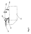
- Fig. 2 shows as electromechanical component 20 a transformer with six connection pins 10, 10a, 60, which is intended to be mounted on a printed circuit board 50.
- the Schonapsbeetzschlagbaren electrically conductive connection pins 10 of the transformer 20 are bent at right angles and are placed on the component side 1 and soldered there. Thus, air creepage distances must be adhered to only on the component side.
- the length of the electrically conductive connection pins 10 is preferably dimensioned so that they protrude after their deformation partially on the transformer outside.
- the bent over the outside of the transformer 20 bent electrically conductive connection pins 10 are easily soldered when the transformer 20 of the board 50 is placed.
- the bent over the outside of the transformer 20 bent electrically conductive connection pin 10 prove to be advantageous
- connection pins 60 and electrically conductive connection pins 10a for which no large air creepage distances apply because they do not carry high voltages are used in the embodiment according to FIG Fig. 2 not bent but are guided and soldered in accordance with the inventive method of the component side 1 through the provided in the circuit board 50 through holes 40.
- the high-voltage electrical connection pins 10 a are usually arranged on the secondary side of the transformer 20.
Landscapes
- Engineering & Computer Science (AREA)
- Manufacturing & Machinery (AREA)
- Microelectronics & Electronic Packaging (AREA)
- Structures For Mounting Electric Components On Printed Circuit Boards (AREA)
Abstract
Description
- Die Erfindung betrifft ein Verfahren zur Montage von elektronischen Bauteilen oder elektromechanischen Komponenten, nachfolgend auch als elektrische Komponenten bezeichnet, auf einer Leiterplatte, nach dem Oberbegriff des Patentanspruches 1 sowie eine Anordnung aus wenigstens einer Leiterplatte zur Aufnahme von elektronischen Bauteilen oder elektromechanischen Komponenten gemäß dem Verfahren nach Anspruch 1.
- Zur Bestückung bzw. Fixierung elektrischer Leiterplatten, auch als gedruckte Schaltungen oder Platinen bezeichnet, mit elektronischen Bauteilen oder elektromechanischen Komponenten sind verschiedene Verfahren bekannt.
- Zur Montage von diskreten Bauteilen, wie beispielsweise Spulen, Widerständen oder Kondensatoren oder von Bauteilen mit einer größeren Abmessung bzw. mit einer großen Masse, wie beispielsweise Transformatoren oder Netzteile zur Strom - und Spannungsversorgung, weisen die elektronischen Bauteile und elektromechanischen Komponenten elektrisch leitende Stifte bzw. Anschlussdrähte - sogenannte Anschlusspins - auf. Zur elektrischen Kontaktierung werden die Anschlusspins auf der Bestückungsseite der Leiterplatte durch vorgesehene Durchgangsbohrungen der Leiterplatte gesteckt und danach auf der gegenüberliegenden Seite, welche auch als Verdrahtungsseite bezeichnet wird, verlötet.
- Durch die auf der Verdrahtungsseite der Leiterplatte aufgebrachten Lötverbindungen zur Fixierung der elektrischen Komponenten wird neben der Bildung einer elektrischen Verbindung zwischen den auf der Leiterplatte befindlichen Leiterbahnen und den elektronischen Komponenten auch eine mechanische Fixierung der Komponenten auf der Leiterplatte erreicht. Dieses Montageverfahren wird auch "Through the hole technology (THT)" genannt.
- Zur Gewährleistung der elektrischen Sicherheit ist es erforderlich vorgegebene Normen einzuhalten, welche zwischen bestimmten Leiteranordnungen Mindestabstände, auch als sogenannte Luft- und Kriechstrecken bekannt, erfordern. Diese Abstände müssen auch auf Leiterplatten, den Luftstrecken und den Zwischenebenen bei einer Durchkontaktierung eingehalten werden. Hier jedoch nur auf den jeweiligen für die Durchkontaktierung genutzten Oberflächen und Ebenen der Leiterplatten, jedoch nicht zwischen den Leiterebenen, da diese durch einen Isolierstoff sicher voneinander isoliert sind, welcher eine sichere elektrische Trennung der Leiter gewährleistet. Dazu wird die Leiterplatte beispielsweise mit einigen elektrischen Komponenten auf der Oberseite der Leiterplatte und einigen elektrischen Komponenten auf der Unterseite einer Leiterplatte bestückt.
- Die vorab beschriebene Anordnung der elektrischen Komponenten und Leiterbahnen auf beiden Seiten der Leiterplatte führt dazu, dass durch die Lötstifte der Komponenten eine leitfähige Verbindung zwischen Ober- und Unterseite sowie allen anderen Leiterebenen geschaffen wird - obwohl eigentlich nur die Kontaktierung einer Leiterplattenseite notwendig wäre. Somit wird es notwendig die vorgegebenen elektrischen Sicherheitsabstände um die Lötverbindungen an den Anschlusspins herum auf allen Ebenen einzuhalten, was die nutzbare Leiterplattenfläche für eine möglichst maximale Ausnutzung der Leiterplattenfläche für die Bestückung und Verdrahtung mit den elektrischen Komponenten erheblich reduziert.
- Eine gegenwärtig bevorzugte Technologie zur Bestückung von Leiterplatten mit elektronischen Bauteilen ist die Oberflächenmontage, auch als "Surface mount devices technology (SMD)" bezeichnet, welche eine bessere Ausnutzung der Leiterplattenfläche ermöglicht. Dabei werden die elektronischen Bauteile direkt auf der Bestückungsseite der Leiterplatte aufgeklebt und die Kontaktstellen der Bauteile mit den auf der Leiterpatte aufgebrachten elektrischen Leiterbahnen verlötet, ohne dass Öffnungen bzw. Durchgangsbohrungen in der Leiterplatte erforderlich sind, und demzufolge keine Pins durch in der Leiterpatte vorzusehende Durchgangsbohrungen gesteckt werden müssen.
- Das SMD-Verfahren eignet sich jedoch nur für Bauteile mit einem geringen Gewicht und geringen Abmessungen. Da die elektronischen Bauteile mittels dem SMD-Verfahren nur auf einer Seite der Leiterplatte befestigt, vorzugsweise geklebt, und verlötet werden, können sich Bauteile großer Masse von der Leiterplatte lösen, weil die SMD-Lötpads sonst abreißen könnten.
- Elektromechanischen Komponenten, wie Transformatoren, Netzteile sowie Kondensatoren oder Spulen größerer Abmessungen, sind auf Grund ihres Gewichtes und/oder ihrer Abmessungen mittels des SMD- Verfahrens nicht mechanisch stabil auf der Leiterplatte montierbar, so dass diese elektromechanischen Komponenten beim Transport der bestückten Leiterplatte oder anderen Erschütterungen abreißen.
- Ausgehend von den beschriebenen Nachteilen liegt der Erfindung demgemäß die Aufgabe zugrunde, die Montage von elektrischen Komponenten, insbesondere von diskreten Bauteilen, wie Spulen, Widerständen oder Kondensatoren sowie von elektromechanischen Komponenten, wie Transformatoren oder Netzteilen in einfacher Weise zu verbessern, und insbesondere eine ausreichende mechanische Stabilität der elektrischen Komponenten auf der Leiterplatte zu erreichen und trotzdem auf der anderen Seite Bauteile bestücken können, weil dort keine Luft-/Kriechstrecken eingehalten werden müssen.
- Diese Aufgabe wird erfindungsgemäß mit den in Anspruch 1 angegebenen Merkmalen gelöst. Vorteilhafte Ausgestaltungen, Verbesserungen der erfindungsgemäßen Einrichtung sowie eine Anordnung zur Aufnahme von elektronischen Komponenten gemäß dem Verfahren nach Anspruch 1 sind in weiteren Ansprüchen und in der Beschreibung angegeben.
- Zur Durchführung des erfindungsgemäßen Verfahrens werden elektronische Bauteilen und/oder elektromechanische Komponenten mit jeweils mehreren Anschlusspins verwendet. Einige dieser Anschlusspins, sogenannte mechanische Anschlusspins oder Leerpins, sind dafür vorgesehen die elektronischen Bauteile und/oder elektromechanischen Komponenten mechanisch sicher auf der Leiterplatte zu befestigen.
- Das erfindungsgemäße Verfahren zur Montage der elektrischen Komponenten auf einer Leiterplatte umfasst die nachfolgend aufgeführten Verfahrensschritte.
- In einem ersten Verfahrensschritt werden Anschlusspins, welche insbesondere zur Einhaltung vorgegebener Normen, wie beispielsweise mit einer Luft-/ und Kriechstrecke von 6,3mm der 230V- Leitungen umgebogen oder abgewinkelt. Mittels der umgebogenen Anschlusspins wird erreicht, dass die jeweilige elektrische Komponente auf der Bestückungsseite der Leiterplatte aufsetzbar ist und das elektrische Potential von anderen Leiterplattenebenen ferngehalten wird. Die umgebogenen Anschlusspins werden im folgendem als mit Strom oder Spannung beaufschlagte Anschlusspins oder elektrisch leitende Anschlusspins bezeichnet.
- In einem zweiten Verfahrensschritt werden die mechanischen Leerpins der elektrischen Komponenten, welche vorab nicht mechanisch verformt bzw. umgebogen wurden durch in der Leiterplatte vorgesehene Durchgangsbohrungen geführt, wodurch die jeweilige elektrische Komponente und die umgebogenen elektrisch leitenden Anschlusspins auf der Bestückungsseite der Leiterplatte aufgesetzt werden.
- In einem abschließenden Verfahrensschritt werden die mechanischen und elektrisch leitenden Anschlusspins fixiert, vorzugsweise verlötet.
- In einer vorteilhaften Ausführungsform des erfindungsgemäßen Verfahrens werden zuerst die durch die Durchgangsbohrungen der Leiterplatte geführten mechanischen Leerpins und danach die elektrisch leitenden Anschlusspins, welche auf der Bestückungsseite der Leiterplatte aufliegen, verlötet. Dadurch wird in vorteilhafter Weise gewährleistet, dass die elektrisch leitenden Anschlusspins nur einer geringen mechanischen Belastung ausgesetzt sind, weil die mechanische Hauptbelastung an den bereits durchgesteckten, verlöteten Pins liegt.
- Mit dem erfindungsgemäßen Verfahren wird somit in vorteilhafter Weise die mechanische Fixierung von elektronischen Bauteile und/oder elektromechanischen Komponenten auf Leiterplatten, die üblicherweise durch den elektrisch-leitenden Anschlusspin gewährleistet wird, von der elektrischen Kontaktierung getrennt und eine mechanisch festere Verbindung der elektrischen Komponenten auf der Leiterplatte erreicht, wobei die durch die Durchgangsbohrungen der Leiterplatte geführten und auf der Verdrahtungsseite der Leiterplatte verlöteten mechanischen Leerpins der Stabilität der elektrischen Komponente dienen und die auf der Bestückungsseite der Leiterplatte aufgesetzten und verlöteten abgewinkelten elektrisch leitenden Anschlusspins zur elektrischen Kontaktierung vorgesehen sind.
- Ein weiterer Vorteil des erfindungsgemäßen Verfahrens beruht darauf, dass durch das Umbiegen der mit Strom oder Spannung beaufschlagbaren Anschlusspins und deren Verlötung auf der Bestückungsseite nur auf der Bestückungsseite die norm-geregelten Anforderungen zu berücksichtigen sind. Dies führt zu einer besseren Auslastung der Bestückungsoberfläche der Leiterplatte und somit zur Einsparung von Leiterplattenfläche; ferner noch einer besseren Auslastung der Leiterbahnfläche der verschiedenen Leiterplattenebenen.
- Eine Anordnung zur Aufnahme von elektronischen Bauteilen und/oder elektromechanischen Komponenten auf einer Leiterplatte mit der die Aufgabe weiterhin gelöst wird, ist dem Anspruch 8 zu entnehmen.
- Die erfindungsgemäße Anordnung umfasst wenigstens eine Leiterplatte zur Aufnahme von elektronischen Bauteilen und/oder elektromechanischen Komponenten, welche mehrere Anschlusspins, auch als Anschlussdrähte bezeichnet, aufweisen.
- Einige dieser Anschlusspins, sogenannte mechanische Anschlusspins oder Leerpins, sind zur mechanisch sicheren Befestigung der elektronischen Bauteile und/oder elektromechanischen Komponenten auf der Leiterplatte vorgesehen.
- Die mit Strom oder Spannung beaufschlagten elektrischen Anschlusspins sind so umbiegbar, dass diese zur Kontaktierung auf der Bestückungsseite der Leiterplatte aufsetzbar sind.
- Die mechanischen Leerpins der elektrischen Komponenten, welche vorab nicht mechanisch verformt bzw. umgebogen wurden, sind durch in der Leiterplatte vorgesehenen Durchgangsbohrungen führbar, wodurch die jeweilige elektrische Komponente und die umgebogenen elektrisch leitenden Anschlusspins auf der Bestückungsseite der Leiterplatte aufsetzbar sind.
- Die Fixierung der elektrischen Komponenten auf der Leiterplatte erfolgt durch ein Verlöten der mechanischen und elektrisch leitenden Anschlusspins.
- Erfindungsgemäß sind nunmehr die mit Strom oder Spannung beaufschlagbaren Anschlusspins auf der Bestückungsseite und die mechanischen Anschlusspins auf der Verdrahtungsseite der Leiterplatte verlötet.
- Die Pins der Niederspannungsseite (Sekundärseite) des Trafos sind zwar elektrisch leitend, müssen aber nicht abgeknickt werden, weil hierbei nur geringe Luft-/und Kriechstrecken erforderlich sind.
- Die mechanischen Anschlusspins sind in einer weiteren Ausführungsform verpressbar. Dazu ist der jeweilige mechanische Anschlusspin als Widerhaken ausgebildet und wird nicht verlötet sondern nur durch die Durchgangsbohrung gesteckt, wodurch kein Lötzinn mehr für diese Komponente benötigt wird.
- In einer bevorzugten Ausführungsform, beispielsweise bei der Bestückung der Leiterplatte mit einem Transformator, ist vorgesehen, die elektrisch leitenden Anschlusspins, welche auf der Bestückungsseite der Leiterplatte aufsetzbar sind, so zu verlängern, dass sie beim Aufsetzen des Transformators auf die Leiterplatte nicht komplett von Gehäuse des Transformators verdeckt werden. Somit wird die Durchführbarkeit des Lötvorganges durch eine verbesserte Zugänglichkeit der elektrisch leitenden Anschlusspins verbessert.
- Um eine geforderte mechanische Stabilität zu gewährleisten, werden in einer besonderen Ausführung der Erfindung zusätzliche Anschlusspins, auch Leerpins genannt, in den Körper der elektrischen Komponente eingebaut. Diese Leerpins werden ebenfalls durch die in der Leiterplatte vorgesehenen Durchgangsbohrungen gesteckt und anschließend der Verdrahtungsseite verlötet.
- Da die Leerpins der elektrischen Komponenten, beispielsweise bei einem Transformator, nunmehr galvanisch von der Hochspannung getrennt trennen sind, unterliegen die Leerpins keinen norm-geregelten Anforderungen für die gegenüberliegende Bestückungsseite der Leiterplatte und die dazwischenliegenden Ebenen.
- Besonders vorteilhaft erweist sich dabei der Einbau von Leerpins in einen Spulenkörper, wobei die Leerpins ebenfalls von der Bestückungsseite der Leiterplatte aus durch die Durchgangsöffnungen in der Leiterplatte geführt werden, um so eine verbesserte mechanische Stabilität zu gewährleisten. Diese zusätzlichen Leerpins sind galvanisch von der Hochspannung getrennt und somit entfallen die norm-geregelten Anforderungen für die gegenüberliegende Bestückungsseite.
- Anhand der in den folgenden Figuren dargestellten Ausführungsbeispiele sollen die Erfindung sowie vorteilhafte Ausgestaltungen, Verbesserungen und weitere Vorteile der Erfindung näher erläutert und beschrieben werden.
- Es zeigen:
- Fig. 1
- eine Ausführungsform der erfindungsgemäßen Anordnung zur Montage von elektrischen Komponenten, und
- Fig. 2
- eine beispielhafte elektromechanische Komponente, welche zur Monta- ge auf einer Leiterplatte vorgesehen ist.
- Unter elektrischen Komponenten sollen elektronische Bauteile oder elektromechanischen Komponenten verstanden werden, welche mehrere Anschlussdrähte oder Anschlusspins 10, 60 aufweisen, die an einer Kontaktierstelle verlötbar sind.
- Die erfindungsgemäße Anordnung wird aus einer Leiterplatte 50 zur Aufnahme von wenigstens einer elektrischen Komponente 20 gebildet, wobei die elektrische Komponente 20 drei Anschlusspins 10 aufweist und nur auf einer Seite, der Bestückungsseite 1 auf die Leiterplatte 50, aufgesetzt ist.
- Ein sogenanntes mechanisches Anschlusspin 60, welches vorab nicht mechanisch verformt bzw. umgebogen wurde, ist zur mechanisch sicheren Befestigung der elektrischen Komponente 20 auf der Leiterplatte 50 vorgesehen. Das mechanische Anschlusspin 60 ist dazu von der Bestückungsseite 1 aus durch eine in der Leiterplatte 50 vorhandene Durchgangsöffnung bzw. -bohrung 40 geführt.
- Die mit Strom oder Spannung beaufschlagten elektrischen Anschlusspins 10 sind so umgebogen, dass diese zur Kontaktierung auf der Bestückungsseite 1 der Leiterplatte 50 aufsetzbar sind.
- Zur Fixierung der elektrischen Komponente 20 auf der Leiterplatte 50 werden die elektrischen und der mechanische Anschlusspin 10, 60 jeweils an einer mit Lotpaste 30 oder Zinnwelle versehenen Kontaktierungsstelle so verlötet, dass die elektrisch leitenden Anschlusspins 10 auf der Bestückungsseite 1 und der mechanischen Anschlusspin 60 auf der Verdrahtungsseite 2 der Leiterplatte 50, vorzugsweise mittels eines automatisch ablaufendem Lötprozesses, verlötet sind.
- Die verlöteten elektrisch leitenden Anschlusspins 10 bilden so die elektrische Kontaktierung der elektrischen Komponente 20 mit auf der Leiterplatte 50 befindlichen Leiterbahnen und der verlötete mechanische Anschlusspin 60 bildet eine mechanisch stabile Verbindung der elektrischen Komponente 20 mit der Leiterplatte 50.
- Somit liegt die mechanische Beanspruchung der elektrischen Komponente 20 vorteilhafterweise an den durch die Durchgangsöffnungen 40 durchgesteckten mechanischen Anschlusspins 60 an und ein Abreißen der elektrischen Komponente 20 von der Leiterplatte wird dadurch minimiert.
-
Fig. 2 zeigt als elektromechanische Komponente 20 einen Transformator mit sechs Anschlusspins 10, 10a, 60, welcher zur Montage auf einer Leiterplatte 50 vorgesehen ist. - Die hochspannungsbeaufschlagbaren elektrisch leitenden Anschlusspins 10 des Transformators 20 sind rechtwinklig abgebogen und werden auf der Bestückungsseite 1 aufgesetzt und dort auch verlötet. Somit müssen Luft-Kriechstrecken nur auf der Bestückungsseite eingehalten werden.
- Bei dem in der
Fig. 2 gezeigten Transformator ist die Länge der elektrisch leitenden Anschlusspins 10 vorzugsweise so bemessen, dass diese nach ihrer Verformung teilweise über die Transformatoraußenseite herausragen. Somit sind die über die Außenseite des Transformators 20 herausragenden umgebogenen elektrisch leitenden Anschlusspins 10 einfach verlötbar, wenn der Transformator 20 der Platine 50 aufgesetzt ist. Insbesondere bei einem manuell ausgeführten Lötvorgang erweisen sich die die über die Außenseite des Transformators 20 herausragenden umgebogenen elektrisch leitenden Anschlusspins 10 als vorteilhaft - Die mechanischen Anschlusspins 60 sowie elektrisch leitende Anschlusspins 10a für die keine großen Luft-Kriechstrecken gelten, weil diese keine hohen Spannungen führen, werden in der Ausführungsform gemäß
Fig. 2 nicht umgebogen sondern werden gemäß dem erfindungsgemäßen Verfahrens von der Bestückungsseite 1 aus durch die in der Leiterplatte 50 vorgesehenen Durchgangsöffnungen 40 geführt und verlötet. - Die keine Hochspannung führenden elektrischen Anschlusspins 10a sind üblicherweise auf der Sekundärseite des Transformators 20 angeordnet.
-
- 1
- Bestückungsseite der Leiterplatte
- 2
- Verdrahtungsseite der Leiterplatte
- 10, 10a
- elektrischer Anschlusspin
- 20
- elektrische Komponente
- 30
- Auftrag der Lotpaste
- 40
- Durchgangsbohrung
- 50
- Leiterplatte
- 60
- mechanischer Anschlusspin
Claims (14)
- Verfahren zur Montage wenigstens einer elektrischen Komponente (20) auf einer Leiterplatte (50), wobei die wenigstens eine elektrische Komponente (20) mehrere elektrisch leitende Anschlusspins (10) sowie wenigstens ein mechanisches Anschlusspin (60) aufweist und auf einer Seite, der Bestückungsseite (1), auf die Leiterplatte (50), aufgesetzt wird, gekennzeichnet durch folgende Verfahrensschritte:a) wenigstens zwei elektrisch leitende Anschlusspins (10) der elektrischen Komponente (20) werden umgebogen,b) das wenigstens eine mechanische Anschlusspin (60) der elektrischen Komponente (20) wird durch eine in der Leiterplatte (50) vorgesehene Durchgangsbohrung (40) geführt, wodurch die jeweilige elektrische Komponente (20) und die umgebogenen elektrisch leitenden Anschlusspins (10) auf der Bestückungsseite (1) der Leiterplatte (50) aufgesetzt werden, undc) nach dem Aufsetzen der elektrischen Komponente (20) auf der Leiterplatte (50) werden die wenigstens zwei umgebogenen elektrisch leitenden Anschlusspins (10) auf der Bestückungsseite (1) der Leiterplatte (50) und die mechanischen Anschlusspins (60) auf der der Bestückungsseite (1) der Leiterplatte (50) gegenüberliegenden Verdrahtungsseite (2) verlötet.
- Verfahren nach Anspruch 1, dadurch gekennzeichnet, dass nur die elektrisch leitenden Anschlusspins (10), welche zur Einhaltung vorgegebener Normen vorgesehen sind, umgebogen und auf der Bestückungsseite (1) verlötet werden.
- Verfahren nach einem der vorherigen Ansprüche, dadurch gekennzeichnet, dass die umgebogenen elektrisch leitenden Anschlusspins (10) mit einer vorgegebenen Länge über die Außenseite der elektrischen Komponente (20) hinausgeführt werden.
- Verfahren nach einem der vorherigen Ansprüche, dadurch gekennzeichnet, dass die elektrischen Komponenten (20) mit zusätzlichen Anschlusspins, auch Leerpins genannt, ausgeführt werden, wobei die Leerpins durch in der Leiterplatte (50) vorgesehene Durchgangsbohrungen (40) gesteckt und auf der Verdrahtungsseite (2) verlötet werden.
- Verfahren nach einem der vorherigen Ansprüche, dadurch gekennzeichnet, dass die Leerpins galvanisch von einer an der elektronisch Komponente (20) anliegenden Hochspannung getrennt werden.
- Verfahren nach einem der vorherigen Ansprüche, dadurch gekennzeichnet, dass zuerst die durch die Durchgangsbohrungen (40) der Leiterplatte (50) geführten Anschlusspins (60), (10a) auf der Verdrahtungsseite (2) und danach die umgebogenen elektrisch leitenden Anschlusspins (10), welche auf der Bestückungsseite (1) der Leiterplatte (50) aufliegen, verlötet werden.
- Verfahren nach einem der vorherigen Ansprüche, dadurch gekennzeichnet, dass elektrisch leitende Anschlusspins (10a), die keine hohen Spannungen führen, nicht umgebogen werden, sondern von der Bestückungsseite (1) aus durch die in der Leiterplatte (50) vorgesehenen Durchgangsöffnungen (40) geführt und verlötet werden.
- Anordnung aus einer Leiterplatte (50) zur Aufnahme von wenigstens einer elektrischen Komponente (20) auf der Leiterplatte (50), wobeia) die wenigstens eine elektrische Komponente (20) mehrere elektrisch leitende Anschlusspins (10) sowie wenigstens ein mechanisches Anschlusspin (60) aufweist und auf einer Seite, der Bestückungsseite (1), auf die Leiterplatte (50), aufsetzbar ist,d) wenigstens zwei elektrisch leitende Anschlusspins (10) der elektrischen Komponente (20) umgebogen sind,e) das wenigstens eine mechanische Anschlusspin (60) der elektrischen Komponente (20) durch eine in der Leiterplatte (50) vorgesehene Durchgangsbohrung (40) geführt ist, wodurch die jeweilige elektrische Komponente (20) und die umgebogenen elektrisch leitenden Anschlusspins (10) auf der Bestückungsseite (1) der Leiterplatte (50) aufgesetzt sind, undb) nach dem Aufsetzen der elektrischen Komponente (20) auf der Leiterplatte (50) die wenigstens zwei umgebogenen elektrisch leitenden Anschlusspins (10) auf der Bestückungsseite (1) der Leiterplatte (50) und die mechanischen Anschlusspins (60) auf der der Bestückungsseite (1) der Leiterplatte (50) gegenüberliegenden Verdrahtungsseite (2) verlötet sind.
- Anordnung nach Anspruch 8, dadurch gekennzeichnet, dass nur die elektrisch leitenden Anschlusspins (10), welche zur Einhaltung vorgegebener Normen vorgesehen sind, umgebogen und auf der Bestückungsseite (1) verlötet sind.
- Anordnung nach einem der Ansprüche 8 oder 9, dadurch gekennzeichnet, dass die umgebogenen elektrisch leitenden Anschlusspins (10) mit einer vorgegebenen Länge über die Außenseite der elektrischen Komponente (20) hinausgeführt sind.
- Anordnung nach einem der Ansprüche 8 bis 10, dadurch gekennzeichnet, dass die elektrischen Komponenten (20) mit zusätzlichen Anschlusspins, auch Leerpins genannt, ausgeführt sind, wobei die Leerpins durch in der Leiterplatte (50) vorgesehene Durchgangsbohrungen (40) gesteckt und auf der Verdrahtungsseite (2) verlötet sind.
- Anordnung nach einem der Ansprüche 8 bis 11, dadurch gekennzeichnet, dass die Leerpins galvanisch von einer an der elektronisch Komponente (20) anliegenden Hochspannung getrennt sind.
- Anordnung nach einem der Ansprüche 8 bis 12, dadurch gekennzeichnet, dass elektrisch leitende Anschlusspins (10a), die keine hohen Spannungen führen, nicht umgebogen sind, sondern von der Bestückungsseite (1) aus durch die in der Leiterplatte (50) vorgesehenen Durchgangsöffnungen (40) geführt und verlötet sind.
- Anordnung nach einem der einem der Ansprüche 8 bis 13, dadurch gekennzeichnet, dass die elektrischen Komponenten elektronische Bauteile und/oder elektromechanischen Komponenten sind.
Applications Claiming Priority (1)
| Application Number | Priority Date | Filing Date | Title |
|---|---|---|---|
| DE102007040662A DE102007040662A1 (de) | 2007-08-27 | 2007-08-27 | Verfahren zur Montage von elektronischen Bauteilen und elektromechanischen Komponenten auf einer Leiterplatte |
Publications (3)
| Publication Number | Publication Date |
|---|---|
| EP2031945A2 true EP2031945A2 (de) | 2009-03-04 |
| EP2031945A3 EP2031945A3 (de) | 2010-05-05 |
| EP2031945B1 EP2031945B1 (de) | 2019-05-01 |
Family
ID=40086468
Family Applications (1)
| Application Number | Title | Priority Date | Filing Date |
|---|---|---|---|
| EP08014607.9A Not-in-force EP2031945B1 (de) | 2007-08-27 | 2008-08-18 | Verfahren zur Montage von elektronischen Bauteilen und elektromechanischen Komponenten auf einer Leiterplatte |
Country Status (2)
| Country | Link |
|---|---|
| EP (1) | EP2031945B1 (de) |
| DE (1) | DE102007040662A1 (de) |
Cited By (2)
| Publication number | Priority date | Publication date | Assignee | Title |
|---|---|---|---|---|
| CN108236780A (zh) * | 2017-12-30 | 2018-07-03 | 杭州速控软件有限公司 | 电动滑板的电路板安装方法 |
| DE102024210243A1 (de) | 2024-10-23 | 2026-04-23 | Volkswagen Aktiengesellschaft | Verfahren zur Montage eines elektrischen Bauteils auf einer Leiterplatte und elektrisches Bauteil |
Families Citing this family (1)
| Publication number | Priority date | Publication date | Assignee | Title |
|---|---|---|---|---|
| DE102023207467A1 (de) | 2023-08-03 | 2025-02-06 | Robert Bosch Gesellschaft mit beschränkter Haftung | Elektrisches Bauelement, insbesondere Transformator |
Citations (1)
| Publication number | Priority date | Publication date | Assignee | Title |
|---|---|---|---|---|
| DE10349956A1 (de) | 2003-10-24 | 2005-06-09 | Endress + Hauser Gmbh + Co. Kg | Leiterplatte mit mindestens einem Bauteil |
Family Cites Families (5)
| Publication number | Priority date | Publication date | Assignee | Title |
|---|---|---|---|---|
| JPS582054A (ja) * | 1981-06-26 | 1983-01-07 | Fujitsu Ltd | 半導体装置 |
| US5506445A (en) * | 1994-06-24 | 1996-04-09 | Hewlett-Packard Company | Optical transceiver module |
| DE19543765B4 (de) * | 1995-11-24 | 2004-09-30 | Loewe Opta Gmbh | Verfahren zur Herstellung von Kontaktzungen und deren Verbindung in an der Unterseite eines elektrischen Bauelements vergesehenen Anschlußstiften |
| SE9901845L (sv) * | 1999-05-20 | 2000-11-21 | Daimler Chrysler Ag | Isolationsbarriär på ett tryckt kretskort |
| US6521842B2 (en) * | 2001-06-20 | 2003-02-18 | International Business Machines Corporation | Hybrid surface mount and pin thru hole circuit board |
-
2007
- 2007-08-27 DE DE102007040662A patent/DE102007040662A1/de not_active Ceased
-
2008
- 2008-08-18 EP EP08014607.9A patent/EP2031945B1/de not_active Not-in-force
Patent Citations (1)
| Publication number | Priority date | Publication date | Assignee | Title |
|---|---|---|---|---|
| DE10349956A1 (de) | 2003-10-24 | 2005-06-09 | Endress + Hauser Gmbh + Co. Kg | Leiterplatte mit mindestens einem Bauteil |
Cited By (3)
| Publication number | Priority date | Publication date | Assignee | Title |
|---|---|---|---|---|
| CN108236780A (zh) * | 2017-12-30 | 2018-07-03 | 杭州速控软件有限公司 | 电动滑板的电路板安装方法 |
| CN108236780B (zh) * | 2017-12-30 | 2019-07-09 | 杭州速控软件有限公司 | 电动滑板的电路板安装方法 |
| DE102024210243A1 (de) | 2024-10-23 | 2026-04-23 | Volkswagen Aktiengesellschaft | Verfahren zur Montage eines elektrischen Bauteils auf einer Leiterplatte und elektrisches Bauteil |
Also Published As
| Publication number | Publication date |
|---|---|
| EP2031945B1 (de) | 2019-05-01 |
| EP2031945A3 (de) | 2010-05-05 |
| DE102007040662A1 (de) | 2009-03-26 |
Similar Documents
| Publication | Publication Date | Title |
|---|---|---|
| DE102017108383B4 (de) | Filter mit Leiterplatte und Stromschienen | |
| DE102017120924B4 (de) | EMV-Filter zur Unterdrückung von Störsignalen | |
| DE102017100381A1 (de) | Filteranordnung | |
| EP1926637A2 (de) | Kombiniertes befestigungs- und kontaktierungssystem für elektrische bauelemente auf übereinander angeordneten leiterplatten | |
| EP2031945B1 (de) | Verfahren zur Montage von elektronischen Bauteilen und elektromechanischen Komponenten auf einer Leiterplatte | |
| DE10340297A1 (de) | Schaltungsanordnung für aktive und passive elektrische und elektronische Bauelemente | |
| WO2008128912A1 (de) | Elektronisches bauelement | |
| EP1085793A2 (de) | Kompakte elektrische Vorrichtung, insbesondere Schaltnetzteil | |
| DE202011005385U1 (de) | Hochstromkontaktelement für Leiterplatten | |
| DE102021120385A1 (de) | Oberflächenmontagetechnik-Anschluss-Header und Verfahren zum Bereitstellen einer elektrischen Verbindung zu einer Leiterplatte | |
| DE102004049575A1 (de) | Elektrisches Anschlusselement und Verfahren zum Anschließen eines Leiterkabels | |
| WO2016000909A1 (de) | Leiterplattenverbindungselement | |
| EP4207956A1 (de) | Fahrzeugscheinwerfermodul | |
| DE10039110A1 (de) | Kompakte elektrische Vorrichtung, insbesondere Schaltnetzteil | |
| EP2037469A1 (de) | Leiterplattenrelais | |
| DE19543765B4 (de) | Verfahren zur Herstellung von Kontaktzungen und deren Verbindung in an der Unterseite eines elektrischen Bauelements vergesehenen Anschlußstiften | |
| DE102024113773B4 (de) | Elektrisches Kontaktierungselement, elektrische Verbindungsanordnung und Verfahren zur Herstellung einer elektrischen Verbindung zwischen Stromschienen und einer Leiterplatte mittels eines Kontaktierungselements | |
| DE3115303A1 (de) | "verfahren zum bestuecken von gedruckten leiterplatten mit drahtlosen miniaturbauelementen und mit solchen miniaturbauelementen bestueckte leiterplatte" | |
| EP0246489A2 (de) | Lötanschlussvorrichtung für elektrische und/oder elektronische Bauteile | |
| EP2120523A2 (de) | Anordnung mit einem Hauptträger und einer Leiterplatte mit Bauelementen | |
| DE102006032441A1 (de) | Vorrichtung aufweisend eine Leiterplatte und ein Modul sowie Verfahren zum Aufbau einer derartigen Vorrichtung | |
| DE202004020191U1 (de) | Einschub-Kontaktierung mittels Schneidklemme | |
| WO2002073746A1 (de) | Leitungsverbinder | |
| DE102024210243A1 (de) | Verfahren zur Montage eines elektrischen Bauteils auf einer Leiterplatte und elektrisches Bauteil | |
| EP4708575A1 (de) | Elektrischer steckverbinder und elektrische steckverbindung |
Legal Events
| Date | Code | Title | Description |
|---|---|---|---|
| PUAI | Public reference made under article 153(3) epc to a published international application that has entered the european phase |
Free format text: ORIGINAL CODE: 0009012 |
|
| AK | Designated contracting states |
Kind code of ref document: A2 Designated state(s): AT BE BG CH CY CZ DE DK EE ES FI FR GB GR HR HU IE IS IT LI LT LU LV MC MT NL NO PL PT RO SE SI SK TR |
|
| AX | Request for extension of the european patent |
Extension state: AL BA MK RS |
|
| PUAL | Search report despatched |
Free format text: ORIGINAL CODE: 0009013 |
|
| AK | Designated contracting states |
Kind code of ref document: A3 Designated state(s): AT BE BG CH CY CZ DE DK EE ES FI FR GB GR HR HU IE IS IT LI LT LU LV MC MT NL NO PL PT RO SE SI SK TR |
|
| AX | Request for extension of the european patent |
Extension state: AL BA MK RS |
|
| 17P | Request for examination filed |
Effective date: 20101013 |
|
| 17Q | First examination report despatched |
Effective date: 20101216 |
|
| AKX | Designation fees paid |
Designated state(s): AT BE BG CH CY CZ DE DK EE ES FI FR GB GR HR HU IE IS IT LI LT LU LV MC MT NL NO PL PT RO SE SI SK TR |
|
| GRAP | Despatch of communication of intention to grant a patent |
Free format text: ORIGINAL CODE: EPIDOSNIGR1 |
|
| STAA | Information on the status of an ep patent application or granted ep patent |
Free format text: STATUS: GRANT OF PATENT IS INTENDED |
|
| INTG | Intention to grant announced |
Effective date: 20190103 |
|
| GRAS | Grant fee paid |
Free format text: ORIGINAL CODE: EPIDOSNIGR3 |
|
| GRAA | (expected) grant |
Free format text: ORIGINAL CODE: 0009210 |
|
| STAA | Information on the status of an ep patent application or granted ep patent |
Free format text: STATUS: THE PATENT HAS BEEN GRANTED |
|
| AK | Designated contracting states |
Kind code of ref document: B1 Designated state(s): AT BE BG CH CY CZ DE DK EE ES FI FR GB GR HR HU IE IS IT LI LT LU LV MC MT NL NO PL PT RO SE SI SK TR |
|
| REG | Reference to a national code |
Ref country code: GB Ref legal event code: FG4D Free format text: NOT ENGLISH |
|
| REG | Reference to a national code |
Ref country code: CH Ref legal event code: EP Ref country code: AT Ref legal event code: REF Ref document number: 1128678 Country of ref document: AT Kind code of ref document: T Effective date: 20190515 |
|
| REG | Reference to a national code |
Ref country code: DE Ref legal event code: R096 Ref document number: 502008016727 Country of ref document: DE |
|
| REG | Reference to a national code |
Ref country code: IE Ref legal event code: FG4D Free format text: LANGUAGE OF EP DOCUMENT: GERMAN |
|
| REG | Reference to a national code |
Ref country code: NL Ref legal event code: MP Effective date: 20190501 |
|
| REG | Reference to a national code |
Ref country code: LT Ref legal event code: MG4D |
|
| PG25 | Lapsed in a contracting state [announced via postgrant information from national office to epo] |
Ref country code: LT Free format text: LAPSE BECAUSE OF FAILURE TO SUBMIT A TRANSLATION OF THE DESCRIPTION OR TO PAY THE FEE WITHIN THE PRESCRIBED TIME-LIMIT Effective date: 20190501 Ref country code: NL Free format text: LAPSE BECAUSE OF FAILURE TO SUBMIT A TRANSLATION OF THE DESCRIPTION OR TO PAY THE FEE WITHIN THE PRESCRIBED TIME-LIMIT Effective date: 20190501 Ref country code: FI Free format text: LAPSE BECAUSE OF FAILURE TO SUBMIT A TRANSLATION OF THE DESCRIPTION OR TO PAY THE FEE WITHIN THE PRESCRIBED TIME-LIMIT Effective date: 20190501 Ref country code: ES Free format text: LAPSE BECAUSE OF FAILURE TO SUBMIT A TRANSLATION OF THE DESCRIPTION OR TO PAY THE FEE WITHIN THE PRESCRIBED TIME-LIMIT Effective date: 20190501 Ref country code: PT Free format text: LAPSE BECAUSE OF FAILURE TO SUBMIT A TRANSLATION OF THE DESCRIPTION OR TO PAY THE FEE WITHIN THE PRESCRIBED TIME-LIMIT Effective date: 20190901 Ref country code: NO Free format text: LAPSE BECAUSE OF FAILURE TO SUBMIT A TRANSLATION OF THE DESCRIPTION OR TO PAY THE FEE WITHIN THE PRESCRIBED TIME-LIMIT Effective date: 20190801 Ref country code: SE Free format text: LAPSE BECAUSE OF FAILURE TO SUBMIT A TRANSLATION OF THE DESCRIPTION OR TO PAY THE FEE WITHIN THE PRESCRIBED TIME-LIMIT Effective date: 20190501 Ref country code: HR Free format text: LAPSE BECAUSE OF FAILURE TO SUBMIT A TRANSLATION OF THE DESCRIPTION OR TO PAY THE FEE WITHIN THE PRESCRIBED TIME-LIMIT Effective date: 20190501 |
|
| PG25 | Lapsed in a contracting state [announced via postgrant information from national office to epo] |
Ref country code: BG Free format text: LAPSE BECAUSE OF FAILURE TO SUBMIT A TRANSLATION OF THE DESCRIPTION OR TO PAY THE FEE WITHIN THE PRESCRIBED TIME-LIMIT Effective date: 20190801 Ref country code: GR Free format text: LAPSE BECAUSE OF FAILURE TO SUBMIT A TRANSLATION OF THE DESCRIPTION OR TO PAY THE FEE WITHIN THE PRESCRIBED TIME-LIMIT Effective date: 20190802 Ref country code: LV Free format text: LAPSE BECAUSE OF FAILURE TO SUBMIT A TRANSLATION OF THE DESCRIPTION OR TO PAY THE FEE WITHIN THE PRESCRIBED TIME-LIMIT Effective date: 20190501 |
|
| PG25 | Lapsed in a contracting state [announced via postgrant information from national office to epo] |
Ref country code: IS Free format text: LAPSE BECAUSE OF FAILURE TO SUBMIT A TRANSLATION OF THE DESCRIPTION OR TO PAY THE FEE WITHIN THE PRESCRIBED TIME-LIMIT Effective date: 20190901 |
|
| PG25 | Lapsed in a contracting state [announced via postgrant information from national office to epo] |
Ref country code: EE Free format text: LAPSE BECAUSE OF FAILURE TO SUBMIT A TRANSLATION OF THE DESCRIPTION OR TO PAY THE FEE WITHIN THE PRESCRIBED TIME-LIMIT Effective date: 20190501 Ref country code: RO Free format text: LAPSE BECAUSE OF FAILURE TO SUBMIT A TRANSLATION OF THE DESCRIPTION OR TO PAY THE FEE WITHIN THE PRESCRIBED TIME-LIMIT Effective date: 20190501 Ref country code: CZ Free format text: LAPSE BECAUSE OF FAILURE TO SUBMIT A TRANSLATION OF THE DESCRIPTION OR TO PAY THE FEE WITHIN THE PRESCRIBED TIME-LIMIT Effective date: 20190501 Ref country code: DK Free format text: LAPSE BECAUSE OF FAILURE TO SUBMIT A TRANSLATION OF THE DESCRIPTION OR TO PAY THE FEE WITHIN THE PRESCRIBED TIME-LIMIT Effective date: 20190501 Ref country code: SK Free format text: LAPSE BECAUSE OF FAILURE TO SUBMIT A TRANSLATION OF THE DESCRIPTION OR TO PAY THE FEE WITHIN THE PRESCRIBED TIME-LIMIT Effective date: 20190501 |
|
| REG | Reference to a national code |
Ref country code: DE Ref legal event code: R097 Ref document number: 502008016727 Country of ref document: DE |
|
| PG25 | Lapsed in a contracting state [announced via postgrant information from national office to epo] |
Ref country code: IT Free format text: LAPSE BECAUSE OF FAILURE TO SUBMIT A TRANSLATION OF THE DESCRIPTION OR TO PAY THE FEE WITHIN THE PRESCRIBED TIME-LIMIT Effective date: 20190501 |
|
| PLBE | No opposition filed within time limit |
Free format text: ORIGINAL CODE: 0009261 |
|
| STAA | Information on the status of an ep patent application or granted ep patent |
Free format text: STATUS: NO OPPOSITION FILED WITHIN TIME LIMIT |
|
| PG25 | Lapsed in a contracting state [announced via postgrant information from national office to epo] |
Ref country code: TR Free format text: LAPSE BECAUSE OF FAILURE TO SUBMIT A TRANSLATION OF THE DESCRIPTION OR TO PAY THE FEE WITHIN THE PRESCRIBED TIME-LIMIT Effective date: 20190501 |
|
| 26N | No opposition filed |
Effective date: 20200204 |
|
| PG25 | Lapsed in a contracting state [announced via postgrant information from national office to epo] |
Ref country code: PL Free format text: LAPSE BECAUSE OF FAILURE TO SUBMIT A TRANSLATION OF THE DESCRIPTION OR TO PAY THE FEE WITHIN THE PRESCRIBED TIME-LIMIT Effective date: 20190501 |
|
| PG25 | Lapsed in a contracting state [announced via postgrant information from national office to epo] |
Ref country code: LU Free format text: LAPSE BECAUSE OF NON-PAYMENT OF DUE FEES Effective date: 20190818 Ref country code: MC Free format text: LAPSE BECAUSE OF FAILURE TO SUBMIT A TRANSLATION OF THE DESCRIPTION OR TO PAY THE FEE WITHIN THE PRESCRIBED TIME-LIMIT Effective date: 20190501 Ref country code: SI Free format text: LAPSE BECAUSE OF FAILURE TO SUBMIT A TRANSLATION OF THE DESCRIPTION OR TO PAY THE FEE WITHIN THE PRESCRIBED TIME-LIMIT Effective date: 20190501 |
|
| REG | Reference to a national code |
Ref country code: BE Ref legal event code: MM Effective date: 20190831 |
|
| PG25 | Lapsed in a contracting state [announced via postgrant information from national office to epo] |
Ref country code: IE Free format text: LAPSE BECAUSE OF NON-PAYMENT OF DUE FEES Effective date: 20190818 |
|
| PG25 | Lapsed in a contracting state [announced via postgrant information from national office to epo] |
Ref country code: BE Free format text: LAPSE BECAUSE OF NON-PAYMENT OF DUE FEES Effective date: 20190831 |
|
| PGFP | Annual fee paid to national office [announced via postgrant information from national office to epo] |
Ref country code: DE Payment date: 20200827 Year of fee payment: 13 Ref country code: FR Payment date: 20200824 Year of fee payment: 13 Ref country code: GB Payment date: 20200825 Year of fee payment: 13 |
|
| PGFP | Annual fee paid to national office [announced via postgrant information from national office to epo] |
Ref country code: AT Payment date: 20200820 Year of fee payment: 13 Ref country code: CH Payment date: 20200821 Year of fee payment: 13 |
|
| PG25 | Lapsed in a contracting state [announced via postgrant information from national office to epo] |
Ref country code: CY Free format text: LAPSE BECAUSE OF FAILURE TO SUBMIT A TRANSLATION OF THE DESCRIPTION OR TO PAY THE FEE WITHIN THE PRESCRIBED TIME-LIMIT Effective date: 20190501 |
|
| PG25 | Lapsed in a contracting state [announced via postgrant information from national office to epo] |
Ref country code: MT Free format text: LAPSE BECAUSE OF FAILURE TO SUBMIT A TRANSLATION OF THE DESCRIPTION OR TO PAY THE FEE WITHIN THE PRESCRIBED TIME-LIMIT Effective date: 20190501 Ref country code: HU Free format text: LAPSE BECAUSE OF FAILURE TO SUBMIT A TRANSLATION OF THE DESCRIPTION OR TO PAY THE FEE WITHIN THE PRESCRIBED TIME-LIMIT; INVALID AB INITIO Effective date: 20080818 |
|
| REG | Reference to a national code |
Ref country code: DE Ref legal event code: R119 Ref document number: 502008016727 Country of ref document: DE |
|
| REG | Reference to a national code |
Ref country code: CH Ref legal event code: PL |
|
| REG | Reference to a national code |
Ref country code: AT Ref legal event code: MM01 Ref document number: 1128678 Country of ref document: AT Kind code of ref document: T Effective date: 20210818 |
|
| GBPC | Gb: european patent ceased through non-payment of renewal fee |
Effective date: 20210818 |
|
| PG25 | Lapsed in a contracting state [announced via postgrant information from national office to epo] |
Ref country code: LI Free format text: LAPSE BECAUSE OF NON-PAYMENT OF DUE FEES Effective date: 20210831 Ref country code: CH Free format text: LAPSE BECAUSE OF NON-PAYMENT OF DUE FEES Effective date: 20210831 Ref country code: AT Free format text: LAPSE BECAUSE OF NON-PAYMENT OF DUE FEES Effective date: 20210818 |
|
| PG25 | Lapsed in a contracting state [announced via postgrant information from national office to epo] |
Ref country code: GB Free format text: LAPSE BECAUSE OF NON-PAYMENT OF DUE FEES Effective date: 20210818 Ref country code: FR Free format text: LAPSE BECAUSE OF NON-PAYMENT OF DUE FEES Effective date: 20210831 Ref country code: DE Free format text: LAPSE BECAUSE OF NON-PAYMENT OF DUE FEES Effective date: 20220301 |