EP2030961A2 - Plasma-resistant ceramics with controlled electrical resistivity - Google Patents
Plasma-resistant ceramics with controlled electrical resistivity Download PDFInfo
- Publication number
- EP2030961A2 EP2030961A2 EP07019163A EP07019163A EP2030961A2 EP 2030961 A2 EP2030961 A2 EP 2030961A2 EP 07019163 A EP07019163 A EP 07019163A EP 07019163 A EP07019163 A EP 07019163A EP 2030961 A2 EP2030961 A2 EP 2030961A2
- Authority
- EP
- European Patent Office
- Prior art keywords
- oxide
- molar
- ceramic
- article
- accordance
- Prior art date
- Legal status (The legal status is an assumption and is not a legal conclusion. Google has not performed a legal analysis and makes no representation as to the accuracy of the status listed.)
- Withdrawn
Links
Images

Classifications
-
- C—CHEMISTRY; METALLURGY
- C04—CEMENTS; CONCRETE; ARTIFICIAL STONE; CERAMICS; REFRACTORIES
- C04B—LIME, MAGNESIA; SLAG; CEMENTS; COMPOSITIONS THEREOF, e.g. MORTARS, CONCRETE OR LIKE BUILDING MATERIALS; ARTIFICIAL STONE; CERAMICS; REFRACTORIES; TREATMENT OF NATURAL STONE
- C04B35/00—Shaped ceramic products characterised by their composition; Ceramics compositions; Processing powders of inorganic compounds preparatory to the manufacturing of ceramic products
- C04B35/50—Shaped ceramic products characterised by their composition; Ceramics compositions; Processing powders of inorganic compounds preparatory to the manufacturing of ceramic products based on rare-earth compounds
- C04B35/505—Shaped ceramic products characterised by their composition; Ceramics compositions; Processing powders of inorganic compounds preparatory to the manufacturing of ceramic products based on rare-earth compounds based on yttrium oxide
-
- C—CHEMISTRY; METALLURGY
- C04—CEMENTS; CONCRETE; ARTIFICIAL STONE; CERAMICS; REFRACTORIES
- C04B—LIME, MAGNESIA; SLAG; CEMENTS; COMPOSITIONS THEREOF, e.g. MORTARS, CONCRETE OR LIKE BUILDING MATERIALS; ARTIFICIAL STONE; CERAMICS; REFRACTORIES; TREATMENT OF NATURAL STONE
- C04B35/00—Shaped ceramic products characterised by their composition; Ceramics compositions; Processing powders of inorganic compounds preparatory to the manufacturing of ceramic products
- C04B35/01—Shaped ceramic products characterised by their composition; Ceramics compositions; Processing powders of inorganic compounds preparatory to the manufacturing of ceramic products based on oxide ceramics
- C04B35/48—Shaped ceramic products characterised by their composition; Ceramics compositions; Processing powders of inorganic compounds preparatory to the manufacturing of ceramic products based on oxide ceramics based on zirconium or hafnium oxides, zirconates, zircon or hafnates
- C04B35/486—Fine ceramics
-
- C—CHEMISTRY; METALLURGY
- C04—CEMENTS; CONCRETE; ARTIFICIAL STONE; CERAMICS; REFRACTORIES
- C04B—LIME, MAGNESIA; SLAG; CEMENTS; COMPOSITIONS THEREOF, e.g. MORTARS, CONCRETE OR LIKE BUILDING MATERIALS; ARTIFICIAL STONE; CERAMICS; REFRACTORIES; TREATMENT OF NATURAL STONE
- C04B35/00—Shaped ceramic products characterised by their composition; Ceramics compositions; Processing powders of inorganic compounds preparatory to the manufacturing of ceramic products
- C04B35/01—Shaped ceramic products characterised by their composition; Ceramics compositions; Processing powders of inorganic compounds preparatory to the manufacturing of ceramic products based on oxide ceramics
- C04B35/495—Shaped ceramic products characterised by their composition; Ceramics compositions; Processing powders of inorganic compounds preparatory to the manufacturing of ceramic products based on oxide ceramics based on vanadium, niobium, tantalum, molybdenum or tungsten oxides or solid solutions thereof with other oxides, e.g. vanadates, niobates, tantalates, molybdates or tungstates
-
- C—CHEMISTRY; METALLURGY
- C04—CEMENTS; CONCRETE; ARTIFICIAL STONE; CERAMICS; REFRACTORIES
- C04B—LIME, MAGNESIA; SLAG; CEMENTS; COMPOSITIONS THEREOF, e.g. MORTARS, CONCRETE OR LIKE BUILDING MATERIALS; ARTIFICIAL STONE; CERAMICS; REFRACTORIES; TREATMENT OF NATURAL STONE
- C04B35/00—Shaped ceramic products characterised by their composition; Ceramics compositions; Processing powders of inorganic compounds preparatory to the manufacturing of ceramic products
- C04B35/50—Shaped ceramic products characterised by their composition; Ceramics compositions; Processing powders of inorganic compounds preparatory to the manufacturing of ceramic products based on rare-earth compounds
-
- C—CHEMISTRY; METALLURGY
- C04—CEMENTS; CONCRETE; ARTIFICIAL STONE; CERAMICS; REFRACTORIES
- C04B—LIME, MAGNESIA; SLAG; CEMENTS; COMPOSITIONS THEREOF, e.g. MORTARS, CONCRETE OR LIKE BUILDING MATERIALS; ARTIFICIAL STONE; CERAMICS; REFRACTORIES; TREATMENT OF NATURAL STONE
- C04B2235/00—Aspects relating to ceramic starting mixtures or sintered ceramic products
- C04B2235/02—Composition of constituents of the starting material or of secondary phases of the final product
- C04B2235/30—Constituents and secondary phases not being of a fibrous nature
- C04B2235/32—Metal oxides, mixed metal oxides, or oxide-forming salts thereof, e.g. carbonates, nitrates, (oxy)hydroxides, chlorides
- C04B2235/3217—Aluminum oxide or oxide forming salts thereof, e.g. bauxite, alpha-alumina
-
- C—CHEMISTRY; METALLURGY
- C04—CEMENTS; CONCRETE; ARTIFICIAL STONE; CERAMICS; REFRACTORIES
- C04B—LIME, MAGNESIA; SLAG; CEMENTS; COMPOSITIONS THEREOF, e.g. MORTARS, CONCRETE OR LIKE BUILDING MATERIALS; ARTIFICIAL STONE; CERAMICS; REFRACTORIES; TREATMENT OF NATURAL STONE
- C04B2235/00—Aspects relating to ceramic starting mixtures or sintered ceramic products
- C04B2235/02—Composition of constituents of the starting material or of secondary phases of the final product
- C04B2235/30—Constituents and secondary phases not being of a fibrous nature
- C04B2235/32—Metal oxides, mixed metal oxides, or oxide-forming salts thereof, e.g. carbonates, nitrates, (oxy)hydroxides, chlorides
- C04B2235/3217—Aluminum oxide or oxide forming salts thereof, e.g. bauxite, alpha-alumina
- C04B2235/3222—Aluminates other than alumino-silicates, e.g. spinel (MgAl2O4)
-
- C—CHEMISTRY; METALLURGY
- C04—CEMENTS; CONCRETE; ARTIFICIAL STONE; CERAMICS; REFRACTORIES
- C04B—LIME, MAGNESIA; SLAG; CEMENTS; COMPOSITIONS THEREOF, e.g. MORTARS, CONCRETE OR LIKE BUILDING MATERIALS; ARTIFICIAL STONE; CERAMICS; REFRACTORIES; TREATMENT OF NATURAL STONE
- C04B2235/00—Aspects relating to ceramic starting mixtures or sintered ceramic products
- C04B2235/02—Composition of constituents of the starting material or of secondary phases of the final product
- C04B2235/30—Constituents and secondary phases not being of a fibrous nature
- C04B2235/32—Metal oxides, mixed metal oxides, or oxide-forming salts thereof, e.g. carbonates, nitrates, (oxy)hydroxides, chlorides
- C04B2235/3224—Rare earth oxide or oxide forming salts thereof, e.g. scandium oxide
-
- C—CHEMISTRY; METALLURGY
- C04—CEMENTS; CONCRETE; ARTIFICIAL STONE; CERAMICS; REFRACTORIES
- C04B—LIME, MAGNESIA; SLAG; CEMENTS; COMPOSITIONS THEREOF, e.g. MORTARS, CONCRETE OR LIKE BUILDING MATERIALS; ARTIFICIAL STONE; CERAMICS; REFRACTORIES; TREATMENT OF NATURAL STONE
- C04B2235/00—Aspects relating to ceramic starting mixtures or sintered ceramic products
- C04B2235/02—Composition of constituents of the starting material or of secondary phases of the final product
- C04B2235/30—Constituents and secondary phases not being of a fibrous nature
- C04B2235/32—Metal oxides, mixed metal oxides, or oxide-forming salts thereof, e.g. carbonates, nitrates, (oxy)hydroxides, chlorides
- C04B2235/3224—Rare earth oxide or oxide forming salts thereof, e.g. scandium oxide
- C04B2235/3225—Yttrium oxide or oxide-forming salts thereof
-
- C—CHEMISTRY; METALLURGY
- C04—CEMENTS; CONCRETE; ARTIFICIAL STONE; CERAMICS; REFRACTORIES
- C04B—LIME, MAGNESIA; SLAG; CEMENTS; COMPOSITIONS THEREOF, e.g. MORTARS, CONCRETE OR LIKE BUILDING MATERIALS; ARTIFICIAL STONE; CERAMICS; REFRACTORIES; TREATMENT OF NATURAL STONE
- C04B2235/00—Aspects relating to ceramic starting mixtures or sintered ceramic products
- C04B2235/02—Composition of constituents of the starting material or of secondary phases of the final product
- C04B2235/30—Constituents and secondary phases not being of a fibrous nature
- C04B2235/32—Metal oxides, mixed metal oxides, or oxide-forming salts thereof, e.g. carbonates, nitrates, (oxy)hydroxides, chlorides
- C04B2235/3224—Rare earth oxide or oxide forming salts thereof, e.g. scandium oxide
- C04B2235/3229—Cerium oxides or oxide-forming salts thereof
-
- C—CHEMISTRY; METALLURGY
- C04—CEMENTS; CONCRETE; ARTIFICIAL STONE; CERAMICS; REFRACTORIES
- C04B—LIME, MAGNESIA; SLAG; CEMENTS; COMPOSITIONS THEREOF, e.g. MORTARS, CONCRETE OR LIKE BUILDING MATERIALS; ARTIFICIAL STONE; CERAMICS; REFRACTORIES; TREATMENT OF NATURAL STONE
- C04B2235/00—Aspects relating to ceramic starting mixtures or sintered ceramic products
- C04B2235/02—Composition of constituents of the starting material or of secondary phases of the final product
- C04B2235/30—Constituents and secondary phases not being of a fibrous nature
- C04B2235/32—Metal oxides, mixed metal oxides, or oxide-forming salts thereof, e.g. carbonates, nitrates, (oxy)hydroxides, chlorides
- C04B2235/3231—Refractory metal oxides, their mixed metal oxides, or oxide-forming salts thereof
- C04B2235/3244—Zirconium oxides, zirconates, hafnium oxides, hafnates, or oxide-forming salts thereof
-
- C—CHEMISTRY; METALLURGY
- C04—CEMENTS; CONCRETE; ARTIFICIAL STONE; CERAMICS; REFRACTORIES
- C04B—LIME, MAGNESIA; SLAG; CEMENTS; COMPOSITIONS THEREOF, e.g. MORTARS, CONCRETE OR LIKE BUILDING MATERIALS; ARTIFICIAL STONE; CERAMICS; REFRACTORIES; TREATMENT OF NATURAL STONE
- C04B2235/00—Aspects relating to ceramic starting mixtures or sintered ceramic products
- C04B2235/02—Composition of constituents of the starting material or of secondary phases of the final product
- C04B2235/30—Constituents and secondary phases not being of a fibrous nature
- C04B2235/32—Metal oxides, mixed metal oxides, or oxide-forming salts thereof, e.g. carbonates, nitrates, (oxy)hydroxides, chlorides
- C04B2235/3231—Refractory metal oxides, their mixed metal oxides, or oxide-forming salts thereof
- C04B2235/3251—Niobium oxides, niobates, tantalum oxides, tantalates, or oxide-forming salts thereof
-
- C—CHEMISTRY; METALLURGY
- C04—CEMENTS; CONCRETE; ARTIFICIAL STONE; CERAMICS; REFRACTORIES
- C04B—LIME, MAGNESIA; SLAG; CEMENTS; COMPOSITIONS THEREOF, e.g. MORTARS, CONCRETE OR LIKE BUILDING MATERIALS; ARTIFICIAL STONE; CERAMICS; REFRACTORIES; TREATMENT OF NATURAL STONE
- C04B2235/00—Aspects relating to ceramic starting mixtures or sintered ceramic products
- C04B2235/02—Composition of constituents of the starting material or of secondary phases of the final product
- C04B2235/30—Constituents and secondary phases not being of a fibrous nature
- C04B2235/32—Metal oxides, mixed metal oxides, or oxide-forming salts thereof, e.g. carbonates, nitrates, (oxy)hydroxides, chlorides
- C04B2235/3231—Refractory metal oxides, their mixed metal oxides, or oxide-forming salts thereof
- C04B2235/3251—Niobium oxides, niobates, tantalum oxides, tantalates, or oxide-forming salts thereof
- C04B2235/3255—Niobates or tantalates, e.g. silver niobate
-
- C—CHEMISTRY; METALLURGY
- C04—CEMENTS; CONCRETE; ARTIFICIAL STONE; CERAMICS; REFRACTORIES
- C04B—LIME, MAGNESIA; SLAG; CEMENTS; COMPOSITIONS THEREOF, e.g. MORTARS, CONCRETE OR LIKE BUILDING MATERIALS; ARTIFICIAL STONE; CERAMICS; REFRACTORIES; TREATMENT OF NATURAL STONE
- C04B2235/00—Aspects relating to ceramic starting mixtures or sintered ceramic products
- C04B2235/02—Composition of constituents of the starting material or of secondary phases of the final product
- C04B2235/30—Constituents and secondary phases not being of a fibrous nature
- C04B2235/40—Metallic constituents or additives not added as binding phase
- C04B2235/404—Refractory metals
-
- C—CHEMISTRY; METALLURGY
- C04—CEMENTS; CONCRETE; ARTIFICIAL STONE; CERAMICS; REFRACTORIES
- C04B—LIME, MAGNESIA; SLAG; CEMENTS; COMPOSITIONS THEREOF, e.g. MORTARS, CONCRETE OR LIKE BUILDING MATERIALS; ARTIFICIAL STONE; CERAMICS; REFRACTORIES; TREATMENT OF NATURAL STONE
- C04B2235/00—Aspects relating to ceramic starting mixtures or sintered ceramic products
- C04B2235/70—Aspects relating to sintered or melt-casted ceramic products
- C04B2235/74—Physical characteristics
- C04B2235/76—Crystal structural characteristics, e.g. symmetry
- C04B2235/762—Cubic symmetry, e.g. beta-SiC
-
- C—CHEMISTRY; METALLURGY
- C04—CEMENTS; CONCRETE; ARTIFICIAL STONE; CERAMICS; REFRACTORIES
- C04B—LIME, MAGNESIA; SLAG; CEMENTS; COMPOSITIONS THEREOF, e.g. MORTARS, CONCRETE OR LIKE BUILDING MATERIALS; ARTIFICIAL STONE; CERAMICS; REFRACTORIES; TREATMENT OF NATURAL STONE
- C04B2235/00—Aspects relating to ceramic starting mixtures or sintered ceramic products
- C04B2235/70—Aspects relating to sintered or melt-casted ceramic products
- C04B2235/74—Physical characteristics
- C04B2235/77—Density
-
- C—CHEMISTRY; METALLURGY
- C04—CEMENTS; CONCRETE; ARTIFICIAL STONE; CERAMICS; REFRACTORIES
- C04B—LIME, MAGNESIA; SLAG; CEMENTS; COMPOSITIONS THEREOF, e.g. MORTARS, CONCRETE OR LIKE BUILDING MATERIALS; ARTIFICIAL STONE; CERAMICS; REFRACTORIES; TREATMENT OF NATURAL STONE
- C04B2235/00—Aspects relating to ceramic starting mixtures or sintered ceramic products
- C04B2235/70—Aspects relating to sintered or melt-casted ceramic products
- C04B2235/80—Phases present in the sintered or melt-cast ceramic products other than the main phase
-
- C—CHEMISTRY; METALLURGY
- C04—CEMENTS; CONCRETE; ARTIFICIAL STONE; CERAMICS; REFRACTORIES
- C04B—LIME, MAGNESIA; SLAG; CEMENTS; COMPOSITIONS THEREOF, e.g. MORTARS, CONCRETE OR LIKE BUILDING MATERIALS; ARTIFICIAL STONE; CERAMICS; REFRACTORIES; TREATMENT OF NATURAL STONE
- C04B2235/00—Aspects relating to ceramic starting mixtures or sintered ceramic products
- C04B2235/70—Aspects relating to sintered or melt-casted ceramic products
- C04B2235/80—Phases present in the sintered or melt-cast ceramic products other than the main phase
- C04B2235/81—Materials characterised by the absence of phases other than the main phase, i.e. single phase materials
-
- Y—GENERAL TAGGING OF NEW TECHNOLOGICAL DEVELOPMENTS; GENERAL TAGGING OF CROSS-SECTIONAL TECHNOLOGIES SPANNING OVER SEVERAL SECTIONS OF THE IPC; TECHNICAL SUBJECTS COVERED BY FORMER USPC CROSS-REFERENCE ART COLLECTIONS [XRACs] AND DIGESTS
- Y10—TECHNICAL SUBJECTS COVERED BY FORMER USPC
- Y10T—TECHNICAL SUBJECTS COVERED BY FORMER US CLASSIFICATION
- Y10T428/00—Stock material or miscellaneous articles
- Y10T428/31—Surface property or characteristic of web, sheet or block
Definitions
- the present application is related to a series of applications which have common inventorship with the present application. All of the applications listed below relate to the use of a yttrium-oxide comprising ceramic to provide a plasma-resistant surface which is useful in semiconductor processing apparatus.
- the related applications include U.S. Application No. 11/796,210, of Sun et al., filed April 27, 2007 , titled:
- Embodiments of the present invention relate to a specialized yttrium oxide-comprising ceramic which is mainly comprised of solid solution ceramic which is highly resistant to plasmas of the kind which are present in semiconductor processing apparatus.
- Corrosion (including erosion) resistance is a critical property for apparatus components and liners used in semiconductor processing chambers, where corrosive environments are present.
- corrosive plasmas are present in the majority of semiconductor processing environments, including plasma enhanced chemical vapor deposition (PECVD) and physical vapor deposition (PVD), the most corrosive plasma environments are those used for cleaning of processing apparatus and those used to etch semiconductor substrates. This is especially true where high-energy plasma is present and combined with chemical reactivity to act upon the surface of components present in the environment.
- the reduced chemical reactivity of an apparatus component surface or of a process chamber liner surface is an important property when corrosive gases, even in the absence of a plasma, are in contact with processing apparatus surfaces.
- Process chamber liners and component apparatus present within the processing chambers used to fabricate electronic devices and micro-electro-mechanical systems (MEMS) are frequently constructed from aluminum and aluminum alloys. Surfaces of the process chamber and component apparatus (present within the chamber) are frequently anodized to provide a degree of protection from the corrosive environment. However, the integrity of the anodization layer may be deteriorated by impurities in the aluminum or aluminum alloy, so that corrosion begins to occur early, shortening the life span of the protective coating.
- the plasma resistance properties of aluminum oxide are not positive in comparison with some other ceramic materials. As a result, ceramic coatings of various compositions have been used in place of the aluminum oxide layer mentioned above; and, in some instances, have been used over the surface of the anodized layer to improve the protection of the underlying aluminum-based materials.
- Yttrium oxide is a ceramic material which has shown considerable promise in the protection of aluminum and aluminum alloy surfaces which are exposed to halogen-containing plasmas of the kind used in the fabrication of semiconductor devices.
- An yttrium oxide coating has been used and applied over an anodized surface of a high purity aluminum alloy process chamber surface, or a process component surface, to produce excellent corrosion protection (e.g. U.S. Patent No. 6,777,873 to Sun et al. , mentioned above).
- the protective coating may be applied using a method such as spray coating, physical vapor deposition (PVD) of chemical vapor deposition (CVD) by way of example.
- a film of Al 2 O 3 , or Al 2 O 3 and Y 2 O 3 has been formed on an inner wall surface of a processing chamber and on those exposed surfaces of the members within the chamber which require a high corrosion resistance and insulating property.
- a base material of the chamber may be a ceramic material (Al 2 O 3 , SiO 2 , AIN, etc.), aluminum, or stainless steel, or other metal or metal alloy, which has a sprayed film over the base material.
- the film may be made of a compound of a III-B element of the periodic table, such as Y 2 O 3
- the film may substantially comprise Al 2 O 3 and Y 2 O 3 .
- a sprayed film of yttrium-aluminum-garnet (YAG) has also been mentioned. Examples of a sprayed film thickness range from 50 ⁇ m to 300 ⁇ m.
- Specialty sintered ceramic materials have been developed which resist corrosion under semiconductor processing conditions which employ a halogen-containing plasma.
- the specialty materials have been modified to have improved plasma resistance and tailored mechanical properties in comparison with the sintered ceramic materials previously used for semiconductor processing apparatus.
- the electrical properties of the sintered ceramic materials have been adjusted so that the electrical resistivity properties of the materials (which have an effect in a plasma processing chamber) meet the requirements of critical chamber components. These electrical resistivity property requirements were previously met only by materials which exhibited low plasma resistance properties.
- the present specialty materials (which offer various combinations of plasma resistance, mechanical properties, and electrical resistivity properties) are sufficiently similar to those of semiconductor processing apparatus previously used.
- One advantage of the similar electrical properties is that it is not necessary to change the process recipes or general processing conditions which are currently in use in semiconductor device fabrication.
- the specialty sintered ceramic material used to fabricate semiconductor processing chamber components may be applied over an underlying material using thermal/flame spraying or plasma spraying, physical vapor deposition (such as sputtering from a target comprised of the specialty sintered ceramic material) or chemical vapor deposition, by way of example.
- the sintered ceramic material may be used to fabricate a solid component using a molding process, for example, when this is preferable to use of a coating.
- the sintered ceramic materials of interest comprise a yttrium oxide-based solid solutions.
- the electrical resistivity of the sintered, yttrium oxide-comprising ceramic material is altered.
- other oxides are added to the yttrium oxide, and the mixture is sintered.
- the positive ions of the other oxides have a different valence from the Y 3+ ion, to form a Y vacancy, leading to a decrease of electrical resistivity.
- examples of such other oxides include CeO 2 , TiO 2 , ZrO 2 , HfO 2 , and Nb 2 O 5 , by way of example and not by way of limitation.
- oxides are added to the yttrium oxide and the mixture is sintered.
- the positive ions of the other oxide show the same valence as the Y 3+ ion, but possess a significantly different ion radius than the Y 3+ ion.
- the precursor mixture is sintered in a reductive atmosphere. This results in an O vacancy, which also decreases electrical resistivity.
- oxides which show the same valence as the Y 3+ ion, but possess a significantly different ion radius include Nd 2 O 3 , Sm 2 O 3 , Sc 2 O 3 , Yb 2 O 3 , Er 2 O 3 , Ho 2 O 3 and Dy 2 O 3 , by way of example and not by way of limitation.
- One of the major components in a semiconductor processing chamber which requires a lower resistivity than is typical for yttrium-comprising sintered ceramics is the electrostatic chuck.
- the electrostatic chuck designers recommend that the resistivity of the dielectric surface of the electrostatic chuck fall within a range from about 10 9 to 10 11 ⁇ cm under semiconductor processing conditions, to reduce the possibility of plasma arcing at the electrostatic chuck.
- This resistivity range is equivalent to a conductivity within a range from about 10 -9 to 10 -7 S/m. This is a considerably lower resistivity than bulk Si 3 N 4 , for example, which exhibits a conductivity 10 -13 S/m.
- a resistivity in the range of that required for an electrostatic chuck is helpful.
- the resistivity may be higher, possible as high as or exceeding about 10 14 ⁇ cm and still be acceptable.
- At least one solid solution forms the major molar % of sintered ceramic materials which are useful as electrically modified corrosion-resistant materials.
- these oxides typically comprise yttrium oxide in combination with another oxide, which is typically selected from the group consisting of zirconium oxide, cerium oxide, hafnium oxide, niobium oxide, and combinations thereof.
- Use of other oxides such as scandium oxide, neodymium oxide, samarium oxide, ytterbium oxides, erbium oxide, and cerium oxide (and other lanthanide series element oxides) is considered to be acceptable in some instances.
- these oxides typically comprise yttrium oxide, zirconium oxide, and at least one other oxide, which is typically selected from the group consisting of hafnium oxide, scandium oxide, neodymium oxide, niobium oxide, samarium oxide, ytterbium oxide, erbium oxide, cerium oxide, and combinations thereof.
- the sintered ceramics comprise multi solid solution phases, typically there are two phases or three phases. In addition to the at least one solid solution-phase, there may be other phases within the sintered ceramic which are compounds or elemental metals.
- a sintered ceramic comprising a solid solution, where yttrium oxide is present over a range from about 40 molar % to less than 100 molar %, and zirconium oxide is present over a range from more than 0 molar % to about 60 molar %, produces a sintered oxide having a resistivity which is in the range from about 10 7 to about 10 15 ⁇ ⁇ cm at room temperature.
- Resistivity over the same range is expected to be obtained from a combination of precursor oxides where yttrium oxide is present over a range from more than 0 molar % to less than 100 molar %, and cerium oxide is present over a range from greater than 0 molar % up to less than 10 molar %.
- Resistivity over a range from about 10 9 to about 10 11 ⁇ ⁇ cm is also expected to be obtained from a combination of precursor oxides where yttrium oxide is present over a range from more than 0 molar % to less than 100 mole %, and hafnium oxide is present over a range from more than 0 molar % up to less than 100 molar %.
- Sintered ceramic exhibiting a resistivity over a range of about 10 9 to about 10 1 ⁇ ⁇ cm is also expected to be obtained from a combination of precursor oxides where yttrium oxide is present over a range from about 48 molar % to less than 100 mole %, and niobium oxide is present over a range from greater than 0 % up to about 52 molar %.
- a sintered ceramic will exhibit a resistivity over a range of about 10 7 to about 10 15 ⁇ ⁇ cm when the sintered ceramic comprises a solid solution, and where the sintered ceramic material is formed from oxides where: yttrium oxide is present over a range from about 40 molar % to less than 100 molar %; zirconium oxide is present over a range from more than 0 molar % to about 50 molar %; and, scandium oxide is present over a range from more than about 0 molar % up to less than 100 molar %.
- a sintered ceramic will exhibit an electrical resistivity over a range of about 10 7 to about 10 15 ⁇ ⁇ cm when the sintered ceramic comprises a solid solution, and the sintered ceramic material is fabricated from oxides where: yttrium oxide is present over a range from about 40 molar % to less than 10 molar %; zirconium oxide is present over a range from more than 0 molar % to about 50 molar %, and hafnium oxide is present over a range from more than about 0 molar % up to less than 100 molar %.
- a sintered ceramic will exhibit a resistivity over a range of about 10 7 to about 10 15 ⁇ ⁇ cm when the sintered ceramic comprises a solid solution, and the sintered ceramic material is fabricated from oxides where:
- the sintered ceramic material contains three phases, which include: a first phase solid solution comprising Y 2 O 3 -ZrO 2 -Nb 2 O 5 which makes up from about 60 molar % to about 90 molar % of the sintered ceramic material; a second phase of Y 3 NbO 7 which makes up from about 5 molar % to about 30 molar % of the sintered ceramic material; and, a third phase ofNb in elemental form, which makes up from about 1 molar % to about 10 molar % of the sintered ceramic material.
- a first phase solid solution comprising Y 2 O 3 -ZrO 2 -Nb 2 O 5 which makes up from about 60 molar % to about 90 molar % of the sintered ceramic material
- a second phase of Y 3 NbO 7 which makes up from about 5 molar % to about 30 molar % of the sintered ceramic material
- a third phase ofNb in elemental form which makes up from about 1
- yttrium oxide is present over a range from about 60 molar % to about 75 molar %; zirconium oxide is present over a range from about 15 molar % to about 25 molar %, and niobium oxide is present over a range from about 5 molar % to about 15 molar %.
- the plasma source power was up to 2000W, the process chamber pressure was 10 - 500 mTorr, and the substrate temperature was 40 °C. This erosion rate of 0.16 ⁇ m/hour or less is equivalent to the erosion rate of pure Y 2 O 3 . Thus, the erosion rate of the sintered ceramics has been unaffected by the modification of the sintered ceramic to provide a lower resistivity sintered ceramic.
- the starting material compositions listed above may be used to form a ceramic coating over the surface of a variety of metal and ceramic substrates, including, but not limited to, aluminum, aluminum alloy, stainless steel, alumina, aluminum nitride and quartz, using a coating technique.
- coating techniques include plasma spraying, thermal/flame spraying; physical vapor deposition from a sputtering target which is formed by sintering the oxides; or, chemical vapor deposition, by way of example and not by way of limitation.
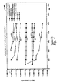
- Figure 1 is a graph 100 illustrating the electrical resistivity, as a function of temperature, for a variety of materials, where the applied voltage was 1000 V in an air environment.
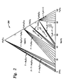
- Figure 2 is a phase diagram 200 of Y 2 O 3 - ZrO 2 - Al 2 O 3 .
- This phase diagram shows, among other compositions, the composition of a specialized material, identified herein as an area "A" on the phase diagram, for reference purposes.
- the type "A" ceramic material is a ceramic composition which has demonstrated excellent resistance to erosion by halogen plasmas.
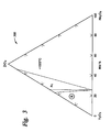
- Figure 3 is a phase diagram 300 of Y 2 O 3 - ZrO 2 - Nb 2 O 5 .
- This phase diagram shows, among other compositions, the composition of a specialized material, identified herein as an area "B" on the phase diagram, for reference purposes.
- the type "B" ceramic material is a ceramic composition which not only resists erosion by halogen plasmas, but which also exhibits a controlled, lower electrical resistivity than the type "A" ceramic material, for example.
- Figure 4 is a graph 400 illustrating electrical resistivity, as a function of applied voltage, for a variety of materials, where the measurement was made at room temperature (about 27 °C) in an air environment.
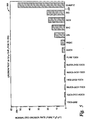
- Figure 5 is a bar chart 500 which shows the average exemplary erosion rate, normalized relative to that for pure yttrium oxide, for a variety of sintered ceramic materials which were exposed to a plasma generated from CF 4 and CHF 3 source gases.
- the specialty materials have been modified to have a reduced electrical resistivity when compared with similar ceramic materials which were developed previously to provide plasma erosion resistance.
- the reduced electrical resistivity is helpful in reducing the possibility of plasma arcing at various components within a semiconductor processing chamber, most notably upon a surface of an electrostatic chuck or a substrate lift pin, where plasma arcing is more of a problem, for example and not by way of limitation.
- the component, or at least the surface of the component was fabricated from aluminum nitride or aluminum oxide, which might be doped to provide electrical properties. While this material provided the desired electrical properties, the corrosion/erosion rate was relatively rapid, limiting the useful lifetime of the particular component, and requiring more down time for repairs and replacement of component parts.
- the electrical properties of the various materials used as process chamber liners and functional components within a plasma processing semiconductor apparatus affect the behavior of the plasma. Changes in the behavior of the plasma affect the plasma processing characteristics, and when the effect is substantial, it is necessary to change other process variables to accommodate the change in the plasma behavior. Rather than rework processing variables for device fabrication, it is more practical to develop erosion resistant ceramic materials which have acceptable electrical properties. Only a portion of the ceramic materials which exhibit acceptable plasma corrosion/erosion characteristics can be modified to control electrical resistivity properties within the desired range useful for a component in contact with plasmas. One skilled in the art and having read the present description will be able to be relatively certain of success when selecting combinations of oxides to form the ceramic materials.
- acceptable halogen plasma corrosion/erosion-resistant ceramic materials having the desired electrical properties were carried out by making use of sintered ceramics.
- the sintered ceramics were produced by techniques well known in the art.
- acceptable halogen plasma corrosion/erosion-resistant ceramic materials of the same general composition may be applied as a coating over an underlying material, such as aluminum or aluminum alloy, for example, using thermal/flame spraying or plasma spraying.
- a sintered ceramic material may be used to fabricate a target which may be used to apply the ceramic material by physical vapor deposition over the underlying material, particularly when the apparatus over which the protective ceramic material is to be applied is large, such as a process chamber liner.
- the sintered ceramic materials of interest comprise yttrium oxide.
- the resistivity of the sintered, yttrium-comprising ceramic material may be altered.
- at least one other oxide is added to the yttrium oxide and the mixture is sintered.
- the positive ions of the at least one other oxide have a different valence from the Y 3+ ion, to form a Y vacancy, leading to a decrease of electrical resistivity.
- oxides include CeO 2 , TiO 2 , ZrO 2 , HfO 2 , and Nb 2 O 5 , by way of example and not by way of limitation.
- the at least one other oxide is added to yttrium oxide, and the mixture is sintered in a reductive atmosphere; however, the positive ions of the at least one other oxide show the same valence as the Y 3+ ion, but possess a significantly different ion radius than the Y 3+ ion. This results in an O vacancy, which also decreases electrical resistivity.
- oxides which show the same valence as the Y 3+ ion, but possess a significantly different ion radius include Nd 2 O 3 , Sm 2 O 3 , Sc 2 O 3 , Yb 2 O 3 , Er 2 O 3 , Ho 2 O 3 and Dy 2 O 3 , by way of example and not by way of limitation.
- Figure 1 shows a graph 100 illustrating electrical resistivity of a variety of ceramic materials, including the Type A and Type B materials made according to exemplary embodiments of the invention.
- the resistivity is shown on axis 104, as a function of temperature, which is shown on axis 102.
- the resistivity was measured at 1000 V in an air environment, using standard test conditions in accordance with ASTM D 1829-66 or JIS C2141.
- Curve 106 shown in Figure 1 is representative of the Nb 2 O 5 -comprising sintered ceramic material which is described as Sample #4 in the Table. With respect to sintered ceramic material comprising Nb 2 O 5 , acceptable electrical resistivity values are expected to be obtained for additional compositions as well, as illustrated by the phase diagram shown in Figure 3 .
- the sintered ceramic material contains three phases, which include a first phase solid solution comprising Y 2 O 3 -ZrO 2 -Nb 2 O 5 which may make up about 60 molar % to about 90 molar % of the sintered ceramic material; a second phase of Y 3 NbO 7 which may make up from about 5 molar % to about 30 molar % of the sintered ceramic material; and, a third phase of Nb in elemental form, which may make up from about 1 molar % to about 10 molar % of the sintered ceramic material.
- This material is particularly useful when the resistivity needs to be low to prevent arcing.
- the resistivity is lower than about 10 11 ⁇ ⁇ cm at room temperature and about 10 8 ⁇ ⁇ cm at 200 °C, and may exhibit a resistivity in the range of 10 9 ⁇ ⁇ cm at typical semiconductor processing conditions.
- Nb 2 O 5 -comprising sintered ceramic material illustrated in Figure 1 is referred to as Nb 2 O 5 - ZrO 2 -Y 2 O 3 .
- one area of the phase diagram has been labeled as "B".
- the solid solution composition of a sintered ceramic material comprises Y 2 O 3 at a concentration ranging from about 55 molar % to about 80 molar %, ZrO 2 at a concentration ranging from about 5 molar % to about 25 molar %, and an additive such as Nb 2 O 5 , HfO 2 , Nd 2 O 3 , or Sc 2 O 3 at a concentration ranging from about 5 molar % to about 25 molar %.
- Curve 108 shown in Figure 1 is representative of the HfO 2 -comprising sintered ceramic material, made in accordance with the present invention, which is also described as Sample #1 in the Table.
- This ceramic material exhibits a higher resistivity than the Nb 2 O 5 -comprising material, but is useful for fabricating semiconductor processing apparatus components where arcing is less critical than with respect to an electrostatic chuck or a substrate lift pin.
- Curve 110 shown in Figure 1 is representative of the Sc 2 O 3 -comprising sintered ceramic material, made in accordance with the present invention, which is also described as Sample 2 in the Table. Again, this material may be used in applications where the resistivity requirement is 10 11 ⁇ ⁇ cm.
- Curve 112 shown in Figure 1 is representative of the Y 2 O 3 - ZrO 2 - Al 2 O 3 material which is illustrated in the Figure 2 phase diagram .
- This material is described for purposes of a comparative example only with respect to the controlled resistivity ceramic materials.
- This sintered ceramic material comprises a solid solution which is formed from Y 2 O 3 and ZrO 2 , and a compound which is formed from Y 2 O 3 and Al 2 O 3 oxides.
- a typical sintered ceramic material is formed from Y 2 O 3 at a concentration ranging from about 60 molar % to about 65 molar %; ZrO 2 at a concentration ranging from about 20 molar % to about 25 molar %; and, Al 2 O 3 at a concentration ranging from about 10 molar % to about 15 molar %.
- One embodiment of a centered ceramic material which is illustrated by area "A" in the phase diagram in Figure 2 , and which is represented by the graph for Y 2 O 3 - ZrO 2 - Al 2 O 3 shown in Figure 1 , contains: about 60 molar % solid solution with a cubic yttria type crystal structure, where c-Y 2 O 3 is a solvent, with Zr 2 O 3 solute; about 2 molar % solid solution with a fluorite type crystal structure, where ZrO 2 is a solvent, with Y 2 O 3 solute; and about 38 molar % YAM (Y 4 Al 2 O 9 ) compound.
- Curve 114 of Figure 1 is representative of the Nd 2 O 3 -comprising sintered ceramic material which is described as Sample #3 in the Table. This material is failed to meet the requirements which are necessary to prevent arcing, and is considered to be a comparative example which is not part of the unique ceramic materials which make up the invention.
- Curve 116 of Figure 1 is representative of the electrical resistivity characteristics observed for a sintered ceramic of pure Y 2 O 3 .
- This material is also a comparative example, which is useful as a baseline, since a number of semiconductor apparatus components have been fabricated from pure Y 2 O 3 .
- a comparison of the resistivity of the pure Y 2 O 3 shows the very significant improvement in terms of electrical resistivity which is achieved by the present invention.
- curves 120 which represents a doped aluminum nitride of the kind commonly used to fabricate an electrostatic chuck
- 122 which represents a second doped aluminum nitride which is also used to fabricate an electrostatic chuck and other semiconductor processing apparatus which requires a low electrical resistivity.
- Figure 4 is a graph 400 which illustrates the electrical resistivity, as a function of the voltage applied during the resistivity testing, for a number of sintered ceramic test specimens.
- the resistivity is shown on axis 404, with the voltage shown on axis 402.
- the test temperature is room temperature (about 27 °C).
- the purpose of this graph is to illustrate the differences in resistivity between the corrosion-resistant ceramic embodiments of the present invention which have been controlled to reduce resistivity and the currently used doped aluminum nitride ceramics. While the doped aluminum nitride ceramics have a somewhat lower resistivity, their corrosion rate is at least 2 times higher than that of the yttrium oxide-comprising ceramics which have been modified to reduce resistivity.
- Curve 422 of Figure 4 represents doped aluminum nitride ceramic of the kind currently used to fabricate an electrostatic chuck.
- Curve 420 represents another doped aluminum nitride ceramic which is used to fabricate an electrostatic chuck and other low resistivity components.
- Curve 406 of Figure 4 is representative of the Nb 2 O 5 -comprising sintered ceramic material which is described as Sample #4 in the Table.
- This yttrium-oxide comprising material which has been modified to reduce resistivity exhibits a resistivity which is very close to that of the doped aluminum nitride identified as AlN-1.
- the corrosion rate of the doped aluminum nitride is more than 10 times faster than the corrosion rate of the yttrium-oxide comprising material illustrated by curve 406, as is shown by the bar chart 500in Figure 5 .
- Curve 408 in Figure 4 is representative of the HfO 2 -comprising sintered ceramic material which is described as Sample #1 in the Table. This ceramic material exhibits a higher resistivity than the Nb 2 O 5 -comprising material, and at room temperature exhibits a resistivity which is outside of the recommended range for components where plasma arcing is more likely to occur. However, at 200 °C, a temperature which is present during some semiconductor processing, the resistivity falls within an acceptable range, as illustrated by Curve 108 in Figure 1 .
- Curve 410 of Figure 4 is representative of the Sc 2 O 3 -comprising sintered ceramic material which is described as Sample 2 in the Table. Again, this material may be used in applications where the resistivity requirement is 10 11 ⁇ ⁇ cm, when the processing temperature is 200 °C.
- Curve 412 of Figure 4 shows a ceramic type "A" material comprising Y 2 O 3 , ZrO 2 , and Al 2 O 3 which is illustrated in Figure 2 .
- a type "A” material which is shown in Figure 1 , contains about 60 molar % cubic yttria type structure with c-Y 2 O 3 as a solvent and with Zr 2 O 3 solute; about 2 molar % fluorite-type structure solid solution with ZrO 2 as a solvent and with Y 2 O 3 solute; and, about 38 molar % YAM (Y 4 Al 2 O 9 ) compound.
- Type A HPM material exhibits acceptable corrosion-resistant properties and commendable mechanical properties, the electrical resistivity is considerably higher that the desired range maximum 10 11 ⁇ ⁇ cm. This is the case even at 200 °C, as illustrated by Curve 112 in Figure 1 . This material is not included among the embodiments for the electrical resistivity modified corrosion resistant ceramics.
- Curve 414 of Figure 4 shows the Nd 2 O 3 - comprising sintered ceramic material which is described as Sample #3 in the Table. This material is failed to meet the requirements which are necessary to prevent arcing, and is considered to be a comparative example which is not part of the unique ceramic materials which make up the invention.
- Curve 416 of figure 4 shows the electrical resistivity characteristics observed for a sintered ceramic of pure Y 2 O 3 .
- This material is also a comparative example, which is useful as a baseline, since a number of semiconductor apparatus components have been fabricated from pure Y 2 O 3 .
- a comparison of the resistivity of the pure Y 2 O 3 shows the very significant improvement in terms of electrical resistivity which is achieved by the present invention.
- Figure 5 illustrates a bar chart 500 which shows the exemplary erosion rate, normalized to pure Y203, for a variety of sintered ceramic materials exposed to a plasma.
- the plasma was generated from CF 4 and CHF 3 source gases.
- the plasma processing chamber was an Enabler for Trench Etch available from Applied Materials, Inc.
- the plasma source power was up to 2000 W, the process chamber pressure was 10 - 500 mTorr, and the substrate temperature was about 40 °C, for a time period of 76 hours.
- the axis 502 shows a variety of materials which were tested for erosion resistance.
- the test specimen identified by a description Y203- 10 ZrO2 represent a sintered solid solution ceramic test specimen which was formed by sintering 100 parts by weight Y2O3 in combination with 10 parts by weight of Zr02.
- the test specimens identified as containing Nb205 -, or Hf02 -, or Nd203 -, or Sc203 - represent the TABLE compositions which are recited as containing each of those materials.
- a comparison of the erosion rates as shown on axis 504 shows that the erosion rates of the resistivity modified, yttrium oxide-comprising sintered ceramic materials are essentially the same as the erosion rate for pure yttrium oxide.
- the erosion rates of the resistivity modified, yttrium oxide-comprising sintered ceramics are substantially better than the erosion rate of Al2O3, AIN, ZrO 2 , Quartz, W/ZrC, B4C and SiC, other ceramic materials which have been used to provide a halogen plasma corrosion- resistant materials for semiconductor processing chamber liners and on semiconductor processing apparatus interior components.
- UV radiation in a plasma environment does not have an effect on leakage current of electrical resistivity-modified yttrium oxide-comprising sintered ceramic materials.
- the ceramic-comprising articles which are useful as semiconductor processing apparatus which is in contact with a plasma include a lid, a liner, a nozzle, a gas distribution plate, a shower head, an electrostatic chuck component, a shadow frame, a substrate-holding frame, a processing kit, and a chamber liner, by way of example and not by way of limitation.
Landscapes
- Chemical & Material Sciences (AREA)
- Engineering & Computer Science (AREA)
- Ceramic Engineering (AREA)
- Structural Engineering (AREA)
- Manufacturing & Machinery (AREA)
- Materials Engineering (AREA)
- Organic Chemistry (AREA)
- Composite Materials (AREA)
- Drying Of Semiconductors (AREA)
- Compositions Of Oxide Ceramics (AREA)
- Container, Conveyance, Adherence, Positioning, Of Wafer (AREA)
- Physical Or Chemical Processes And Apparatus (AREA)
- Physical Vapour Deposition (AREA)
- Chemical Vapour Deposition (AREA)
Abstract
Description
- The present application is related to a series of applications which have common inventorship with the present application. All of the applications listed below relate to the use of a yttrium-oxide comprising ceramic to provide a plasma-resistant surface which is useful in semiconductor processing apparatus. The related applications include
U.S. Application No. 11/796,210, of Sun et al., filed April 27, 2007 - "Method of Reducing The Erosion Rate Of Semiconductor Processing Apparatus Exposed To Halogen-Containing Plasmas", which is currently pending;
U.S. Application No. 11/796,211, of Sun et al., filed April 27, 2007 U.S. Application No. 10/898,113 of Sun et al., filed July 22, 2004 U.S. Application No. 10/918,232 of Sun et al., filed August 13, 2004 U.S. Application No. 10/075,967 of Sun et al., filed February 14, 2002 , titled: "Yttrium Oxide Based Surface Coating For Semiconductor IC Processing Vacuum Chambers", which issued asU.S. Patent No. 6,776,873 on August 17, 2004 . Additional related applications filed, which are a divisional and a continuation application of above-listed applications, include:U.S. Application No. 11/595,484 of Wang et al., filed November 10, 2006 U.S. Application No. 10/898,113 ; andU.S. Application No. 11/592,905 of Wang et al., filed November 3, 2006 U.S. Application No. 10/918,232 . The subject matter of all of these patents and applications is hereby incorporated by reference. - BACKGROUND
- 1. Field
- Embodiments of the present invention relate to a specialized yttrium oxide-comprising ceramic which is mainly comprised of solid solution ceramic which is highly resistant to plasmas of the kind which are present in semiconductor processing apparatus.
- 2. Background Art
- This section describes background subject matter related to the disclosed embodiments of the present invention. There is no intention, either express or implied, that the background art discussed in this section legally constitutes prior art.
- Corrosion (including erosion) resistance is a critical property for apparatus components and liners used in semiconductor processing chambers, where corrosive environments are present. Although corrosive plasmas are present in the majority of semiconductor processing environments, including plasma enhanced chemical vapor deposition (PECVD) and physical vapor deposition (PVD), the most corrosive plasma environments are those used for cleaning of processing apparatus and those used to etch semiconductor substrates. This is especially true where high-energy plasma is present and combined with chemical reactivity to act upon the surface of components present in the environment. The reduced chemical reactivity of an apparatus component surface or of a process chamber liner surface is an important property when corrosive gases, even in the absence of a plasma, are in contact with processing apparatus surfaces.
- Process chamber liners and component apparatus present within the processing chambers used to fabricate electronic devices and micro-electro-mechanical systems (MEMS) are frequently constructed from aluminum and aluminum alloys. Surfaces of the process chamber and component apparatus (present within the chamber) are frequently anodized to provide a degree of protection from the corrosive environment. However, the integrity of the anodization layer may be deteriorated by impurities in the aluminum or aluminum alloy, so that corrosion begins to occur early, shortening the life span of the protective coating. The plasma resistance properties of aluminum oxide are not positive in comparison with some other ceramic materials. As a result, ceramic coatings of various compositions have been used in place of the aluminum oxide layer mentioned above; and, in some instances, have been used over the surface of the anodized layer to improve the protection of the underlying aluminum-based materials.
- Yttrium oxide is a ceramic material which has shown considerable promise in the protection of aluminum and aluminum alloy surfaces which are exposed to halogen-containing plasmas of the kind used in the fabrication of semiconductor devices. An yttrium oxide coating has been used and applied over an anodized surface of a high purity aluminum alloy process chamber surface, or a process component surface, to produce excellent corrosion protection (e.g.
U.S. Patent No. 6,777,873 to Sun et al. , mentioned above). The protective coating may be applied using a method such as spray coating, physical vapor deposition (PVD) of chemical vapor deposition (CVD) by way of example. - A film of Al2O3, or Al2O3 and Y2O3 has been formed on an inner wall surface of a processing chamber and on those exposed surfaces of the members within the chamber which require a high corrosion resistance and insulating property. In an exemplary application, a base material of the chamber may be a ceramic material (Al2O3, SiO2, AIN, etc.), aluminum, or stainless steel, or other metal or metal alloy, which has a sprayed film over the base material. The film may be made of a compound of a III-B element of the periodic table, such as Y2O3 The film may substantially comprise Al2O3 and Y2O3. A sprayed film of yttrium-aluminum-garnet (YAG) has also been mentioned. Examples of a sprayed film thickness range from 50 µm to 300 µm.
- SUMMARY
- Specialty sintered ceramic materials have been developed which resist corrosion under semiconductor processing conditions which employ a halogen-containing plasma. The specialty materials have been modified to have improved plasma resistance and tailored mechanical properties in comparison with the sintered ceramic materials previously used for semiconductor processing apparatus. The electrical properties of the sintered ceramic materials have been adjusted so that the electrical resistivity properties of the materials (which have an effect in a plasma processing chamber) meet the requirements of critical chamber components. These electrical resistivity property requirements were previously met only by materials which exhibited low plasma resistance properties. The present specialty materials (which offer various combinations of plasma resistance, mechanical properties, and electrical resistivity properties) are sufficiently similar to those of semiconductor processing apparatus previously used. One advantage of the similar electrical properties is that it is not necessary to change the process recipes or general processing conditions which are currently in use in semiconductor device fabrication.
- The specialty sintered ceramic material used to fabricate semiconductor processing chamber components may be applied over an underlying material using thermal/flame spraying or plasma spraying, physical vapor deposition (such as sputtering from a target comprised of the specialty sintered ceramic material) or chemical vapor deposition, by way of example. In the alternative, the sintered ceramic material may be used to fabricate a solid component using a molding process, for example, when this is preferable to use of a coating.
- The sintered ceramic materials of interest comprise a yttrium oxide-based solid solutions. In one embodiment, the electrical resistivity of the sintered, yttrium oxide-comprising ceramic material is altered. In one exemplary embodiment technique, other oxides are added to the yttrium oxide, and the mixture is sintered. The positive ions of the other oxides have a different valence from the Y3+ ion, to form a Y vacancy, leading to a decrease of electrical resistivity. Examples of such other oxides include CeO2, TiO2, ZrO2, HfO2, and Nb2O5, by way of example and not by way of limitation. In an alternative exemplary embodiment technique, other oxides are added to the yttrium oxide and the mixture is sintered. The positive ions of the other oxide show the same valence as the Y3+ ion, but possess a significantly different ion radius than the Y3+ ion. The precursor mixture is sintered in a reductive atmosphere. This results in an O vacancy, which also decreases electrical resistivity. Examples of oxides which show the same valence as the Y3+ ion, but possess a significantly different ion radius include Nd2O3, Sm2O3, Sc2O3, Yb2O3, Er2O3, Ho2O3 and Dy2O3, by way of example and not by way of limitation.
- One of the major components in a semiconductor processing chamber which requires a lower resistivity than is typical for yttrium-comprising sintered ceramics is the electrostatic chuck. The electrostatic chuck designers recommend that the resistivity of the dielectric surface of the electrostatic chuck fall within a range from about 109 to 1011 Ω·cm under semiconductor processing conditions, to reduce the possibility of plasma arcing at the electrostatic chuck. This resistivity range is equivalent to a conductivity within a range from about 10-9 to 10-7 S/m. This is a considerably lower resistivity than bulk Si3N4, for example, which exhibits a conductivity 10-13 S/m. For other corrosion resistant surfaces where plasma arcing might be a problem, such as lift pins, a resistivity in the range of that required for an electrostatic chuck is helpful. For corrosion resistant surfaces such as process chamber liners, the resistivity may be higher, possible as high as or exceeding about 1014 Ω·cm and still be acceptable.
- At least one solid solution forms the major molar % of sintered ceramic materials which are useful as electrically modified corrosion-resistant materials. When there are two oxides used to form a solid solution, these oxides typically comprise yttrium oxide in combination with another oxide, which is typically selected from the group consisting of zirconium oxide, cerium oxide, hafnium oxide, niobium oxide, and combinations thereof. Use of other oxides such as scandium oxide, neodymium oxide, samarium oxide, ytterbium oxides, erbium oxide, and cerium oxide (and other lanthanide series element oxides) is considered to be acceptable in some instances.
- When there are more than two oxides used to form the one or more solid solutions, these oxides typically comprise yttrium oxide, zirconium oxide, and at least one other oxide, which is typically selected from the group consisting of hafnium oxide, scandium oxide, neodymium oxide, niobium oxide, samarium oxide, ytterbium oxide, erbium oxide, cerium oxide, and combinations thereof. The use of other lanthanide series elements is also possible in particular instances. When the sintered ceramics comprise multi solid solution phases, typically there are two phases or three phases. In addition to the at least one solid solution-phase, there may be other phases within the sintered ceramic which are compounds or elemental metals.
- By way of example, and not by way or limitation, with respect to sintered ceramics which make use of two precursor oxides, experiments have confirmed that a sintered ceramic comprising a solid solution, where yttrium oxide is present over a range from about 40 molar % to less than 100 molar %, and zirconium oxide is present over a range from more than 0 molar % to about 60 molar %, produces a sintered oxide having a resistivity which is in the range from about 107 to about 1015 Ω ·cm at room temperature. Resistivity over the same range is expected to be obtained from a combination of precursor oxides where yttrium oxide is present over a range from more than 0 molar % to less than 100 molar %, and cerium oxide is present over a range from greater than 0 molar % up to less than 10 molar %. Resistivity over a range from about 109 to about 1011 Ω ·cm is also expected to be obtained from a combination of precursor oxides where yttrium oxide is present over a range from more than 0 molar % to less than 100 mole %, and hafnium oxide is present over a range from more than 0 molar % up to less than 100 molar %. Sintered ceramic exhibiting a resistivity over a range of about 109 to about 101 Ω ·cm is also expected to be obtained from a combination of precursor oxides where yttrium oxide is present over a range from about 48 molar % to less than 100 mole %, and niobium oxide is present over a range from greater than 0 % up to about 52 molar %.
- By way of example, and not by way of limitation, with respect to sintered ceramics which make use of more than two precursor oxides, in one embodiment, a sintered ceramic will exhibit a resistivity over a range of about 107 to about 1015 Ω ·cm when the sintered ceramic comprises a solid solution, and where the sintered ceramic material is formed from oxides where: yttrium oxide is present over a range from about 40 molar % to less than 100 molar %; zirconium oxide is present over a range from more than 0 molar % to about 50 molar %; and, scandium oxide is present over a range from more than about 0 molar % up to less than 100 molar %.
- In another embodiment, a sintered ceramic will exhibit an electrical resistivity over a range of about 107 to about 1015 Ω ·cm when the sintered ceramic comprises a solid solution, and the sintered ceramic material is fabricated from oxides where: yttrium oxide is present over a range from about 40 molar % to less than 10 molar %; zirconium oxide is present over a range from more than 0 molar % to about 50 molar %, and hafnium oxide is present over a range from more than about 0 molar % up to less than 100 molar %.
- In yet another embodiment, a sintered ceramic will exhibit a resistivity over a range of about 107 to about 1015 Ω ·cm when the sintered ceramic comprises a solid solution, and the sintered ceramic material is fabricated from oxides where:
- yttrium oxide is present over a range from about 40 molar % to less than 100 molar %; zirconium oxide is present over a range from more than 0 molar % to about 45 molar %; and, niobium oxide is present over a range from more than about 0 molar % up to about 80 molar %.
- In one embodiment, the sintered ceramic material contains three phases, which include: a first phase solid solution comprising Y2O3-ZrO2-Nb2O5 which makes up from about 60 molar % to about 90 molar % of the sintered ceramic material; a second phase of Y3NbO7 which makes up from about 5 molar % to about 30 molar % of the sintered ceramic material; and, a third phase ofNb in elemental form, which makes up from about 1 molar % to about 10 molar % of the sintered ceramic material.
- In another embodiment of the sintered ceramic material which contains three phases, yttrium oxide is present over a range from about 60 molar % to about 75 molar %; zirconium oxide is present over a range from about 15 molar % to about 25 molar %, and niobium oxide is present over a range from about 5 molar % to about 15 molar %.
- In sintered ceramic test specimens formed from a Y2O3 - ZrO2 - MxOy material of the kind described above, in embodiments where M is scandium, hafnium, niobium, or neodymium, an erosion rate was demonstrated which was 0.16 µm/hour or less, after exposure for 76 hours to a CF4/CHF3 plasma. A similar erosion rate is expected when M is cerium, samarium, erbium, or another lanthanide series element. The plasma was formed in an Enabler for Trench Etch plasma processing chamber available from Applied Materials, Inc. The plasma source power was up to 2000W, the process chamber pressure was 10 - 500 mTorr, and the substrate temperature was 40 °C. This erosion rate of 0.16 µm/hour or less is equivalent to the erosion rate of pure Y2O3. Thus, the erosion rate of the sintered ceramics has been unaffected by the modification of the sintered ceramic to provide a lower resistivity sintered ceramic.
- While the ceramic materials described above were sintered ceramics formed from oxides using sintering techniques known in the art, in other embodiments, the starting material compositions listed above may be used to form a ceramic coating over the surface of a variety of metal and ceramic substrates, including, but not limited to, aluminum, aluminum alloy, stainless steel, alumina, aluminum nitride and quartz, using a coating technique. Such coating techniques include plasma spraying, thermal/flame spraying; physical vapor deposition from a sputtering target which is formed by sintering the oxides; or, chemical vapor deposition, by way of example and not by way of limitation.
- BRIEF DESCRIPTION OF THE DRAWINGS
- To assist in the understanding of the above recited embodiments, a more particular description of specific embodiments described above may be had by reference to the appended drawings. It is to be noted, however, that the appended drawings illustrate only a portion of the typical embodiments, and are not therefore considered to be limiting in scope of the invention which is described herein. The invention includes other equally effective embodiments.
-
Figure 1 is agraph 100 illustrating the electrical resistivity, as a function of temperature, for a variety of materials, where the applied voltage was 1000 V in an air environment. -
Figure 2 is a phase diagram 200 of Y2O3 - ZrO2 - Al2O3. This phase diagram shows, among other compositions, the composition of a specialized material, identified herein as an area "A" on the phase diagram, for reference purposes. The type "A" ceramic material is a ceramic composition which has demonstrated excellent resistance to erosion by halogen plasmas. -
Figure 3 is a phase diagram 300 of Y2O3 - ZrO2 - Nb2O5. This phase diagram shows, among other compositions, the composition of a specialized material, identified herein as an area "B" on the phase diagram, for reference purposes. The type "B" ceramic material is a ceramic composition which not only resists erosion by halogen plasmas, but which also exhibits a controlled, lower electrical resistivity than the type "A" ceramic material, for example. -
Figure 4 is agraph 400 illustrating electrical resistivity, as a function of applied voltage, for a variety of materials, where the measurement was made at room temperature (about 27 °C) in an air environment. -
Figure 5 is abar chart 500 which shows the average exemplary erosion rate, normalized relative to that for pure yttrium oxide, for a variety of sintered ceramic materials which were exposed to a plasma generated from CF4 and CHF3 source gases. - DETAILED DESCRIPTION OF EXEMPLARY EMBODIMENTS
- As a preface to the detailed description, it should be noted that, as used in this specification and the appended claims, the singular forms "a", "an", and "the" include plural referents, unless the context clearly dictates otherwise.
- When the word "about" is used herein, this is intended to mean that the nominal value presented is precise within ± 10 %.
- Described herein are specialized ceramic materials which are developed to resist corrosion under semiconductor device processing conditions which employ a halogen-containing plasma. In certain embodiments, the specialty materials have been modified to have a reduced electrical resistivity when compared with similar ceramic materials which were developed previously to provide plasma erosion resistance. The reduced electrical resistivity is helpful in reducing the possibility of plasma arcing at various components within a semiconductor processing chamber, most notably upon a surface of an electrostatic chuck or a substrate lift pin, where plasma arcing is more of a problem, for example and not by way of limitation. In the past the component, or at least the surface of the component was fabricated from aluminum nitride or aluminum oxide, which might be doped to provide electrical properties. While this material provided the desired electrical properties, the corrosion/erosion rate was relatively rapid, limiting the useful lifetime of the particular component, and requiring more down time for repairs and replacement of component parts.
- Further, the electrical properties of the various materials used as process chamber liners and functional components within a plasma processing semiconductor apparatus affect the behavior of the plasma. Changes in the behavior of the plasma affect the plasma processing characteristics, and when the effect is substantial, it is necessary to change other process variables to accommodate the change in the plasma behavior. Rather than rework processing variables for device fabrication, it is more practical to develop erosion resistant ceramic materials which have acceptable electrical properties. Only a portion of the ceramic materials which exhibit acceptable plasma corrosion/erosion characteristics can be modified to control electrical resistivity properties within the desired range useful for a component in contact with plasmas. One skilled in the art and having read the present description will be able to be relatively certain of success when selecting combinations of oxides to form the ceramic materials.
- For reasons of convenience, the development of acceptable halogen plasma corrosion/erosion-resistant ceramic materials having the desired electrical properties was carried out by making use of sintered ceramics. The sintered ceramics were produced by techniques well known in the art. In other embodiments, acceptable halogen plasma corrosion/erosion-resistant ceramic materials of the same general composition may be applied as a coating over an underlying material, such as aluminum or aluminum alloy, for example, using thermal/flame spraying or plasma spraying. In the alternative, a sintered ceramic material may be used to fabricate a target which may be used to apply the ceramic material by physical vapor deposition over the underlying material, particularly when the apparatus over which the protective ceramic material is to be applied is large, such as a process chamber liner.
- As previously discussed, the sintered ceramic materials of interest comprise yttrium oxide. The resistivity of the sintered, yttrium-comprising ceramic material may be altered. In one exemplary technique, at least one other oxide is added to the yttrium oxide and the mixture is sintered. The positive ions of the at least one other oxide have a different valence from the Y3+ ion, to form a Y vacancy, leading to a decrease of electrical resistivity. Examples of such oxides include CeO2, TiO2, ZrO2, HfO2, and Nb2O5, by way of example and not by way of limitation. In another exemplary technique, the at least one other oxide is added to yttrium oxide, and the mixture is sintered in a reductive atmosphere; however, the positive ions of the at least one other oxide show the same valence as the Y3+ ion, but possess a significantly different ion radius than the Y3+ ion. This results in an O vacancy, which also decreases electrical resistivity. Examples of oxides which show the same valence as the Y3+ ion, but possess a significantly different ion radius include Nd2O3, Sm2O3, Sc2O3, Yb2O3, Er2O3, Ho2O3 and Dy2O3, by way of example and not by way of limitation.
- A number of exemplary sintered ceramic materials have been investigated to date, and the TABLE below provides an illustration of a portion of the sintered ceramic materials which were created and evaluated. The evaluation of these materials is discussed subsequently.
- EXAMPLES:
-
TABLE Sample # Precursor Molar % Precursor Weight % Precursor Weight Parts/100 Y2O3 Melting Point (°C) Sintering Temp. (°C) Phase Comp. Density (g / cm3) 1 Y2O3: 75.0 Y2O3: 77.82 Y2O3: 100.00 2800 >1800 c-ss single phase** 5.607 HfO2: 20.0 HfO2: 19.35 HfO2: 24.86 ZrO2: 5.0 ZrO2: 2.83 ZrO2: 3.64 2 Y2O3: 60.0 Y2O3: 72.18 Y2O3: 100.00 2360 >1800 c-ss single phase** 4.936 Sc2O3: 20.0 Sc2O3: 14.69 Sc2O3: 20.36 ZrO2: 20.0 ZrO2: 13.13 ZrO2: 18.19 3 Y2O3: 60.0 Y2O3: 59.58 Y2O3: 100.00 N/A* >1800 c-ss single phase** 5.555 Nd2O3: 20.0 Nd2O3: 29.58 Nd2O3: 49.66 ZrO2: 20.0 ZrO2: 10.84 ZrO2: 18.19 4 Y2O3: 70.0 Y2O3: 75.53 Y2O3: 100.00 N/A* >1800 c-ss** Y3NbO and Nb 5.331 Nb2O5: 10.0 Nb2O5: 12.7 Nb2O5: 16.82 ZrO2: 20.0 ZrO2: 11.77 ZrO2: 15.59 *N/A = not available
** c-ss means cubic yttria type solid solution. - Example One
-
Figure 1 shows agraph 100 illustrating electrical resistivity of a variety of ceramic materials, including the Type A and Type B materials made according to exemplary embodiments of the invention. The resistivity is shown onaxis 104, as a function of temperature, which is shown onaxis 102. The resistivity was measured at 1000 V in an air environment, using standard test conditions in accordance with ASTM D 1829-66 or JIS C2141. -
Curve 106 shown inFigure 1 is representative of the Nb2O5 -comprising sintered ceramic material which is described as Sample #4 in the Table. With respect to sintered ceramic material comprising Nb2O5, acceptable electrical resistivity values are expected to be obtained for additional compositions as well, as illustrated by the phase diagram shown inFigure 3 . The sintered ceramic material contains three phases, which include a first phase solid solution comprising Y2O3-ZrO2-Nb2O5 which may make up about 60 molar % to about 90 molar % of the sintered ceramic material; a second phase of Y3NbO7 which may make up from about 5 molar % to about 30 molar % of the sintered ceramic material; and, a third phase of Nb in elemental form, which may make up from about 1 molar % to about 10 molar % of the sintered ceramic material. This material is particularly useful when the resistivity needs to be low to prevent arcing. The resistivity is lower than about 1011 Ω ·cm at room temperature and about 108 Ω ·cm at 200 °C, and may exhibit a resistivity in the range of 109 Ω ·cm at typical semiconductor processing conditions. - One embodiment of the Nb2O5-comprising sintered ceramic material illustrated in
Figure 1 is referred to as Nb2O5- ZrO2-Y2O3. With reference toFigure 3 , one area of the phase diagram has been labeled as "B". This designation indicates that the solid solution composition of a sintered ceramic material comprises Y2O3 at a concentration ranging from about 55 molar % to about 80 molar %, ZrO2 at a concentration ranging from about 5 molar % to about 25 molar %, and an additive such as Nb2O5, HfO2, Nd2O3, or Sc2O3 at a concentration ranging from about 5 molar % to about 25 molar %. - Example Two
-
Curve 108 shown inFigure 1 is representative of the HfO2 -comprising sintered ceramic material, made in accordance with the present invention, which is also described asSample # 1 in the Table. This ceramic material exhibits a higher resistivity than the Nb2O5 -comprising material, but is useful for fabricating semiconductor processing apparatus components where arcing is less critical than with respect to an electrostatic chuck or a substrate lift pin. - Example Three
-
Curve 110 shown inFigure 1 is representative of the Sc2O3 -comprising sintered ceramic material, made in accordance with the present invention, which is also described asSample 2 in the Table. Again, this material may be used in applications where the resistivity requirement is 1011 Ω ·cm. - Example Four (Comparative Example)
-
Curve 112 shown inFigure 1 is representative of the Y2O3 - ZrO2 - Al2O3 material which is illustrated in theFigure 2 phase diagram . This material is described for purposes of a comparative example only with respect to the controlled resistivity ceramic materials. This sintered ceramic material comprises a solid solution which is formed from Y2O3 and ZrO2, and a compound which is formed from Y2O3 and Al2O3 oxides. A typical sintered ceramic material is formed from Y2O3 at a concentration ranging from about 60 molar % to about 65 molar %; ZrO2 at a concentration ranging from about 20 molar % to about 25 molar %; and, Al2O3 at a concentration ranging from about 10 molar % to about 15 molar %. One embodiment of a centered ceramic material, which is illustrated by area "A" in the phase diagram inFigure 2 , and which is represented by the graph for Y2O3 - ZrO2 - Al2O3 shown inFigure 1 , contains: about 60 molar % solid solution with a cubic yttria type crystal structure, where c-Y2O3 is a solvent, with Zr2O3 solute; about 2 molar % solid solution with a fluorite type crystal structure, where ZrO2 is a solvent, with Y2O3 solute; and about 38 molar % YAM (Y4Al2O9) compound. - Example Five (Comparative Example)
-
Curve 114 ofFigure 1 is representative of the Nd2O3 -comprising sintered ceramic material which is described asSample # 3 in the Table. This material is failed to meet the requirements which are necessary to prevent arcing, and is considered to be a comparative example which is not part of the unique ceramic materials which make up the invention. - Example Six (Comparative Example)
-
Curve 116 ofFigure 1 is representative of the electrical resistivity characteristics observed for a sintered ceramic of pure Y2O3. This material is also a comparative example, which is useful as a baseline, since a number of semiconductor apparatus components have been fabricated from pure Y2O3. A comparison of the resistivity of the pure Y2O3 shows the very significant improvement in terms of electrical resistivity which is achieved by the present invention. - Also shown in
Figure 1 arecurves 120, which represents a doped aluminum nitride of the kind commonly used to fabricate an electrostatic chuck, and 122 which represents a second doped aluminum nitride which is also used to fabricate an electrostatic chuck and other semiconductor processing apparatus which requires a low electrical resistivity. - Example Seven
-
Figure 4 is agraph 400 which illustrates the electrical resistivity, as a function of the voltage applied during the resistivity testing, for a number of sintered ceramic test specimens. The resistivity is shown onaxis 404, with the voltage shown onaxis 402. The test temperature is room temperature (about 27 °C). The purpose of this graph is to illustrate the differences in resistivity between the corrosion-resistant ceramic embodiments of the present invention which have been controlled to reduce resistivity and the currently used doped aluminum nitride ceramics. While the doped aluminum nitride ceramics have a somewhat lower resistivity, their corrosion rate is at least 2 times higher than that of the yttrium oxide-comprising ceramics which have been modified to reduce resistivity. - In particular,
Curve 422 ofFigure 4 represents doped aluminum nitride ceramic of the kind currently used to fabricate an electrostatic chuck.Curve 420 represents another doped aluminum nitride ceramic which is used to fabricate an electrostatic chuck and other low resistivity components. - Curve 406 of
Figure 4 is representative of the Nb2O5 -comprising sintered ceramic material which is described as Sample #4 in the Table. This yttrium-oxide comprising material which has been modified to reduce resistivity exhibits a resistivity which is very close to that of the doped aluminum nitride identified as AlN-1. Yet, the corrosion rate of the doped aluminum nitride is more than 10 times faster than the corrosion rate of the yttrium-oxide comprising material illustrated by curve 406, as is shown by the bar chart 500inFigure 5 . -
Curve 408 inFigure 4 is representative of the HfO2 -comprising sintered ceramic material which is described asSample # 1 in the Table. This ceramic material exhibits a higher resistivity than the Nb2O5 -comprising material, and at room temperature exhibits a resistivity which is outside of the recommended range for components where plasma arcing is more likely to occur. However, at 200 °C, a temperature which is present during some semiconductor processing, the resistivity falls within an acceptable range, as illustrated byCurve 108 inFigure 1 . -
Curve 410 ofFigure 4 is representative of the Sc2O3 -comprising sintered ceramic material which is described asSample 2 in the Table. Again, this material may be used in applications where the resistivity requirement is 1011 Ω ·cm, when the processing temperature is 200 °C. - For comparative purposes (with respect to a controlled electrical resistivity ceramic containing a yttria-comprising solid solution),
Curve 412 ofFigure 4 shows a ceramic type "A" material comprising Y2O3, ZrO2, and Al2O3 which is illustrated inFigure 2 . One embodiment of such a type "A" material, which is shown inFigure 1 , contains about 60 molar % cubic yttria type structure with c-Y2O3 as a solvent and with Zr2O3 solute; about 2 molar % fluorite-type structure solid solution with ZrO2 as a solvent and with Y2O3 solute; and, about 38 molar % YAM (Y4Al2O9) compound. While the Type A HPM material exhibits acceptable corrosion-resistant properties and commendable mechanical properties, the electrical resistivity is considerably higher that the desired range maximum 1011 Ω ·cm. This is the case even at 200 °C, as illustrated byCurve 112 inFigure 1 . This material is not included among the embodiments for the electrical resistivity modified corrosion resistant ceramics. - For comparative purposes,
Curve 414 ofFigure 4 shows the Nd2O3 - comprising sintered ceramic material which is described asSample # 3 in the Table. This material is failed to meet the requirements which are necessary to prevent arcing, and is considered to be a comparative example which is not part of the unique ceramic materials which make up the invention. - For comparative purposes,
Curve 416 offigure 4 shows the electrical resistivity characteristics observed for a sintered ceramic of pure Y2O3. This material is also a comparative example, which is useful as a baseline, since a number of semiconductor apparatus components have been fabricated from pure Y2O3. A comparison of the resistivity of the pure Y2O3 shows the very significant improvement in terms of electrical resistivity which is achieved by the present invention. - Example Eight
-
Figure 5 illustrates abar chart 500 which shows the exemplary erosion rate, normalized to pure Y203, for a variety of sintered ceramic materials exposed to a plasma. The plasma was generated from CF4 and CHF3 source gases. The plasma processing chamber was an Enabler for Trench Etch available from Applied Materials, Inc. The plasma source power was up to 2000 W, the process chamber pressure was 10 - 500 mTorr, and the substrate temperature was about 40 °C, for a time period of 76 hours. The axis 502 shows a variety of materials which were tested for erosion resistance. The test specimen identified by a description Y203- 10 ZrO2, represent a sintered solid solution ceramic test specimen which was formed by sintering 100 parts by weight Y2O3 in combination with 10 parts by weight of Zr02. The test specimens identified as containing Nb205 -, or Hf02 -, or Nd203 -, or Sc203 - represent the TABLE compositions which are recited as containing each of those materials. A comparison of the erosion rates as shown onaxis 504 shows that the erosion rates of the resistivity modified, yttrium oxide-comprising sintered ceramic materials are essentially the same as the erosion rate for pure yttrium oxide. Further, the erosion rates of the resistivity modified, yttrium oxide-comprising sintered ceramics are substantially better than the erosion rate of Al2O3, AIN, ZrO2, Quartz, W/ZrC, B4C and SiC, other ceramic materials which have been used to provide a halogen plasma corrosion- resistant materials for semiconductor processing chamber liners and on semiconductor processing apparatus interior components. - Based on the results obtained during the experimentation which provided the examples described above, and data from other reference sources, calculations have been made which provide estimates of the effect of UV radiation in plasma leakage current. UV radiation in a plasma environment (of the kind used in semiconductor processing) does not have an effect on leakage current of electrical resistivity-modified yttrium oxide-comprising sintered ceramic materials.
- An investigation of the affect of 193 nm UV irradiation (which is employed in some semiconductor processing operations) on the leakage current in the Nb2O5 - Type B sintered ceramic material and the HfO2 - Type B sintered ceramic material has indicated that the electrical performance of these materials should not be affected by such UV irradiation.
- The ceramic-comprising articles which are useful as semiconductor processing apparatus which is in contact with a plasma include a lid, a liner, a nozzle, a gas distribution plate, a shower head, an electrostatic chuck component, a shadow frame, a substrate-holding frame, a processing kit, and a chamber liner, by way of example and not by way of limitation.
- The above described exemplary embodiments are not intended to limit the scope of the present invention, as one skilled in the art can, in view of the present disclosure, expand such embodiments to correspond with the subject matter of the invention claimed below.
Claims (22)
- A ceramic-comprising article which is resistant to erosion by halogen-containing plasmas used in semiconductor processing and which exhibits a controlled electrical resistivity in the range of about 10-7 to 10-15 Ω ·cm at a temperature ranging from about 350 °C to room temperature, said ceramic article having a surface comprising at least one solid solution containing yttrium oxide, and wherein at least one solid solution which comprises yttrium oxide also contains at one or more oxides selected from the group consisting of zirconium oxide, hafnium oxide, scandium oxide, niobium oxide, samarium oxide, ytterbium oxide, erbium oxide, cerium oxide, and combinations thereof.
- A ceramic-comprising article in accordance with Claim 1, where other lanthanide series element oxides are included in said ceramic article.
- A ceramic-comprising article in accordance with Claim 1, wherein two oxides are used to form said at least one solid solution which comprises yttrium oxide and an other oxide, and wherein said other oxide is selected from the group consisting of zirconium oxide, cerium oxide, hafnium oxide, and niobium oxide.
- A ceramic-comprising article in accordance with Claim 3, wherein scandium oxide, samarium oxide, ytterbium oxide, erbium oxide, or an other lanthanide series element oxide is included in said ceramic article.
- A ceramic-comprising article in accordance with Claim 1, wherein more than two precursor oxides are used to form said solid solution which comprises yttrium oxide, and wherein said precursor oxides include zirconium oxide and another oxide selected from the group consisting of hafnium oxide, scandium oxide, niobium oxide, samarium oxide, ytterbium oxide, erbium oxide, cerium oxide, and combinations thereof.
- A ceramic-comprising article in accordance with Claim 5, wherein other lanthanide series elements are included in said ceramic-comprising article.
- A ceramic-comprising article in accordance with Claim 3, wherein said ceramic is formed from yttrium oxide at a concentration ranging from about 40 molar % to less than 100 molar %, and zirconium oxide at concentration ranging from more than 0 molar % to about 60 molar %.
- A ceramic-comprising article in accordance with Claim 3, wherein said ceramic is formed from yttrium oxide at a concentration ranging from about 40 molar % to less than 100 molar %, and cerium oxide at concentration ranging from greater than 0 molar % to about 60 molar %.
- A ceramic-comprising article in accordance with Claim 3, wherein said ceramic is formed from yttrium oxide at a concentration ranging from about 40 molar % to less than 100 molar %, and hafnium oxide at concentration ranging from greater than 0 molar % to about 60 molar %.
- A ceramic-comprising article in accordance with Claim 3, wherein said ceramic is formed from yttrium oxide at a concentration ranging from about 40 molar % to less than 100 molar %, and niobium oxide at concentration ranging from greater than 0 molar % to about 60 molar %.
- A ceramic-comprising article in accordance with Claim 5, wherein yttrium oxide is present at a concentration ranging from about 40 molar % to less than 100 molar %, zirconium oxide is present over a range from more than 0 molar % to about 20 molar %, and scandium oxide is present over a range from more than 0 molar % up to less than 100 molar %.
- A ceramic-comprising article in accordance with Claim 5, wherein yttrium oxide is present at a concentration ranging from about 70 molar % to less than 100 molar %, zirconium oxide is present over a range from more than 0 molar % to about 17 molar %, and hafnium oxide is present over a range from more than 0 molar % up to about 27 molar %.
- A ceramic-comprising article in accordance with Claim 5, wherein said article is formed from a three phase sintered ceramic which includes a first phase of solid solution comprising Y2O3-ZrO2-Nb2O5 which makes up from about 60 molar % to about 90 molar % of the sintered ceramic material; a second phase of Y3NbO7 which makes up from about 5 molar % to about 30 molar % of the sintered ceramic material; and, a third phase of Nb in elemental form, which makes up from about 1 molar % to about 10 molar % of the sintered ceramic material.
- A ceramic-comprising article in accordance with Claim 1, wherein said article is in the form of an electrostatic chuck or a substrate lift pin figure, or another article which requires an electrical resistivity in the range of about 10-7 to 10-15 Ω ·cm at a temperature which ranges from about 350 °C to room temperature.
- A ceramic-comprising article in accordance with Claim 1, wherein said article is in the form of an internal component or a liner used in the interior of a semiconductor processing chamber, and wherein the resistivity of said ceramic article is in the range of about 10-7 to 10-15 Ω ·cm at a temperature which ranges from about 350 °C to room temperature.
- A ceramic-comprising article in accordance with Claim 1, wherein said article is a solid sintered ceramic article.
- A ceramic-comprising article in accordance with Claim 1, wherein said article is selected from the group consisting of an electrostatic chuck, a lid, a liner, a nozzle, a gas distribution plate, a shower head, an electrostatic chuck component, a shadow frame, a substrate holding frame, a processing kit, and a chamber liner.
- A ceramic-comprising article in accordance with Claim 1, wherein said surface of said article is coated with said ceramic.
- A method of reducing plasma arcing within a semiconductor processing chamber which employs an electrostatic chuck, a liner or an internal component having a surface which is in contact with a plasma, said surface comprising a ceramic material, said method comprising:a) selecting oxides to comprise said ceramic material from yttrium oxide and at least one other oxide, where a positive ions of said other oxide has a significantly different valance from a Y3+ ion, to form a Y vacancy, leading to a decrease of electronic resistivity of said ceramic material;b) sintering said oxides to form at least one crystalline solid solution; andc) exposing said ceramic material to a plasma.
- A method in accordance with Claim 19, wherein said oxide having said different valance from said Y3+ ion is selected from the group consisting of CeO2, TiO2, ZrO2, HfO2, Nb2O5, and combinations thereof.
- A method of reducing plasma arcing within a semiconductor processing chamber which employs an electrostatic chuck, a liner or an internal component having a surface contacting a plasma, said surface comprising a ceramic material, said method comprising:a) selecting oxides to comprise said ceramic material from yttrium oxide and at least one other oxide, where a positive ion of said other oxide shows the same valence as the Y3+ ion, but possess a significantly different ion radius than the Y3+ ion, leading to a decrease of electronic resistivity of said ceramic material;b) sintering said oxides in a reductive atmosphere; andc) exposing said ceramic material to a plasma.
- A method in accordance with Claim 21, wherein said oxide having said significantly different ion radius is selected from the group consisting of Nd2O3, Sm2O3, Sc2O3, Yb2O3, Er2O3, Ho2O3, Dy2O3, and combinations thereof.
Applications Claiming Priority (1)
| Application Number | Priority Date | Filing Date | Title |
|---|---|---|---|
| US11/890,156 US8367227B2 (en) | 2007-08-02 | 2007-08-02 | Plasma-resistant ceramics with controlled electrical resistivity |
Publications (2)
| Publication Number | Publication Date |
|---|---|
| EP2030961A2 true EP2030961A2 (en) | 2009-03-04 |
| EP2030961A3 EP2030961A3 (en) | 2009-08-12 |
Family
ID=40229937
Family Applications (1)
| Application Number | Title | Priority Date | Filing Date |
|---|---|---|---|
| EP07019163A Withdrawn EP2030961A3 (en) | 2007-08-02 | 2007-09-28 | Plasma-resistant ceramics with controlled electrical resistivity |
Country Status (7)
| Country | Link |
|---|---|
| US (2) | US8367227B2 (en) |
| EP (1) | EP2030961A3 (en) |
| JP (2) | JP2009035469A (en) |
| KR (1) | KR100934516B1 (en) |
| CN (2) | CN104710178A (en) |
| SG (1) | SG149811A1 (en) |
| TW (1) | TWI361177B (en) |
Cited By (1)
| Publication number | Priority date | Publication date | Assignee | Title |
|---|---|---|---|---|
| US10074552B2 (en) * | 2014-02-26 | 2018-09-11 | Tokyo Electron Limited | Method of manufacturing electrostatic chuck having dot structure on surface thereof |
Families Citing this family (455)
| Publication number | Priority date | Publication date | Assignee | Title |
|---|---|---|---|---|
| US7371467B2 (en) | 2002-01-08 | 2008-05-13 | Applied Materials, Inc. | Process chamber component having electroplated yttrium containing coating |
| US20080264564A1 (en) * | 2007-04-27 | 2008-10-30 | Applied Materials, Inc. | Method of reducing the erosion rate of semiconductor processing apparatus exposed to halogen-containing plasmas |
| US7479304B2 (en) * | 2002-02-14 | 2009-01-20 | Applied Materials, Inc. | Gas distribution plate fabricated from a solid yttrium oxide-comprising substrate |
| JP4936948B2 (en) * | 2007-03-27 | 2012-05-23 | 日本碍子株式会社 | Composite material and manufacturing method thereof |
| US10622194B2 (en) | 2007-04-27 | 2020-04-14 | Applied Materials, Inc. | Bulk sintered solid solution ceramic which exhibits fracture toughness and halogen plasma resistance |
| US10242888B2 (en) | 2007-04-27 | 2019-03-26 | Applied Materials, Inc. | Semiconductor processing apparatus with a ceramic-comprising surface which exhibits fracture toughness and halogen plasma resistance |
| US8367227B2 (en) * | 2007-08-02 | 2013-02-05 | Applied Materials, Inc. | Plasma-resistant ceramics with controlled electrical resistivity |
| WO2010024354A1 (en) * | 2008-08-29 | 2010-03-04 | Toto株式会社 | Electrostatic chuck and method for producing same |
| JP2010064937A (en) * | 2008-09-12 | 2010-03-25 | Covalent Materials Corp | Ceramic for plasma treatment apparatuses |
| US9394608B2 (en) | 2009-04-06 | 2016-07-19 | Asm America, Inc. | Semiconductor processing reactor and components thereof |
| US8802201B2 (en) | 2009-08-14 | 2014-08-12 | Asm America, Inc. | Systems and methods for thin-film deposition of metal oxides using excited nitrogen-oxygen species |
| US20110198034A1 (en) * | 2010-02-11 | 2011-08-18 | Jennifer Sun | Gas distribution showerhead with coating material for semiconductor processing |
| JP2012074650A (en) * | 2010-09-30 | 2012-04-12 | Samco Inc | Plasma treatment tray and plasma treatment device |
| US10283321B2 (en) | 2011-01-18 | 2019-05-07 | Applied Materials, Inc. | Semiconductor processing system and methods using capacitively coupled plasma |
| US9064815B2 (en) | 2011-03-14 | 2015-06-23 | Applied Materials, Inc. | Methods for etch of metal and metal-oxide films |
| US20130023129A1 (en) | 2011-07-20 | 2013-01-24 | Asm America, Inc. | Pressure transmitter for a semiconductor processing environment |
| JP2013079155A (en) * | 2011-09-30 | 2013-05-02 | Covalent Materials Corp | Plasma resistant member |
| JP5526098B2 (en) * | 2011-09-30 | 2014-06-18 | コバレントマテリアル株式会社 | Corrosion-resistant member and manufacturing method thereof |
| US9017481B1 (en) | 2011-10-28 | 2015-04-28 | Asm America, Inc. | Process feed management for semiconductor substrate processing |
| US9034199B2 (en) | 2012-02-21 | 2015-05-19 | Applied Materials, Inc. | Ceramic article with reduced surface defect density and process for producing a ceramic article |
| US9212099B2 (en) | 2012-02-22 | 2015-12-15 | Applied Materials, Inc. | Heat treated ceramic substrate having ceramic coating and heat treatment for coated ceramics |
| US9090046B2 (en) | 2012-04-16 | 2015-07-28 | Applied Materials, Inc. | Ceramic coated article and process for applying ceramic coating |
| US9394615B2 (en) | 2012-04-27 | 2016-07-19 | Applied Materials, Inc. | Plasma resistant ceramic coated conductive article |
| US9267739B2 (en) | 2012-07-18 | 2016-02-23 | Applied Materials, Inc. | Pedestal with multi-zone temperature control and multiple purge capabilities |
| US9604249B2 (en) | 2012-07-26 | 2017-03-28 | Applied Materials, Inc. | Innovative top-coat approach for advanced device on-wafer particle performance |
| US9343289B2 (en) | 2012-07-27 | 2016-05-17 | Applied Materials, Inc. | Chemistry compatible coating material for advanced device on-wafer particle performance |
| US9373517B2 (en) | 2012-08-02 | 2016-06-21 | Applied Materials, Inc. | Semiconductor processing with DC assisted RF power for improved control |
| US9132436B2 (en) | 2012-09-21 | 2015-09-15 | Applied Materials, Inc. | Chemical control features in wafer process equipment |
| US20140099794A1 (en) * | 2012-09-21 | 2014-04-10 | Applied Materials, Inc. | Radical chemistry modulation and control using multiple flow pathways |
| US10714315B2 (en) | 2012-10-12 | 2020-07-14 | Asm Ip Holdings B.V. | Semiconductor reaction chamber showerhead |
| KR101421112B1 (en) * | 2012-10-26 | 2014-07-21 | 한양대학교 산학협력단 | Method of manufacturing plasma resistant member by electrostatic slurry spray deposition and method of manufacturing lift pin by the same |
| US9916998B2 (en) | 2012-12-04 | 2018-03-13 | Applied Materials, Inc. | Substrate support assembly having a plasma resistant protective layer |
| US9685356B2 (en) * | 2012-12-11 | 2017-06-20 | Applied Materials, Inc. | Substrate support assembly having metal bonded protective layer |
| US8941969B2 (en) | 2012-12-21 | 2015-01-27 | Applied Materials, Inc. | Single-body electrostatic chuck |
| US9358702B2 (en) | 2013-01-18 | 2016-06-07 | Applied Materials, Inc. | Temperature management of aluminium nitride electrostatic chuck |
| US20160376700A1 (en) | 2013-02-01 | 2016-12-29 | Asm Ip Holding B.V. | System for treatment of deposition reactor |
| US10256079B2 (en) | 2013-02-08 | 2019-04-09 | Applied Materials, Inc. | Semiconductor processing systems having multiple plasma configurations |
| US9362130B2 (en) | 2013-03-01 | 2016-06-07 | Applied Materials, Inc. | Enhanced etching processes using remote plasma sources |
| US9669653B2 (en) | 2013-03-14 | 2017-06-06 | Applied Materials, Inc. | Electrostatic chuck refurbishment |
| US9887121B2 (en) | 2013-04-26 | 2018-02-06 | Applied Materials, Inc. | Protective cover for electrostatic chuck |
| US9666466B2 (en) | 2013-05-07 | 2017-05-30 | Applied Materials, Inc. | Electrostatic chuck having thermally isolated zones with minimal crosstalk |
| US9708713B2 (en) | 2013-05-24 | 2017-07-18 | Applied Materials, Inc. | Aerosol deposition coating for semiconductor chamber components |
| US9865434B2 (en) | 2013-06-05 | 2018-01-09 | Applied Materials, Inc. | Rare-earth oxide based erosion resistant coatings for semiconductor application |
| US9850568B2 (en) | 2013-06-20 | 2017-12-26 | Applied Materials, Inc. | Plasma erosion resistant rare-earth oxide based thin film coatings |
| US9711334B2 (en) | 2013-07-19 | 2017-07-18 | Applied Materials, Inc. | Ion assisted deposition for rare-earth oxide based thin film coatings on process rings |
| US9583369B2 (en) | 2013-07-20 | 2017-02-28 | Applied Materials, Inc. | Ion assisted deposition for rare-earth oxide based coatings on lids and nozzles |
| US20150079370A1 (en) | 2013-09-18 | 2015-03-19 | Applied Materials, Inc. | Coating architecture for plasma sprayed chamber components |
| US9637415B2 (en) | 2013-10-24 | 2017-05-02 | Surmet Corporation | Method of making high purity polycrystalline aluminum oxynitride bodies useful in semiconductor process chambers |
| US9440886B2 (en) | 2013-11-12 | 2016-09-13 | Applied Materials, Inc. | Rare-earth oxide based monolithic chamber material |
| US9725799B2 (en) | 2013-12-06 | 2017-08-08 | Applied Materials, Inc. | Ion beam sputtering with ion assisted deposition for coatings on chamber components |
| US11015245B2 (en) | 2014-03-19 | 2021-05-25 | Asm Ip Holding B.V. | Gas-phase reactor and system having exhaust plenum and components thereof |
| US9869013B2 (en) | 2014-04-25 | 2018-01-16 | Applied Materials, Inc. | Ion assisted deposition top coat of rare-earth oxide |
| US9976211B2 (en) | 2014-04-25 | 2018-05-22 | Applied Materials, Inc. | Plasma erosion resistant thin film coating for high temperature application |
| US10730798B2 (en) | 2014-05-07 | 2020-08-04 | Applied Materials, Inc. | Slurry plasma spray of plasma resistant ceramic coating |
| US10196728B2 (en) | 2014-05-16 | 2019-02-05 | Applied Materials, Inc. | Plasma spray coating design using phase and stress control |
| US10858737B2 (en) | 2014-07-28 | 2020-12-08 | Asm Ip Holding B.V. | Showerhead assembly and components thereof |
| US9460898B2 (en) | 2014-08-08 | 2016-10-04 | Applied Materials, Inc. | Plasma generation chamber with smooth plasma resistant coating |
| US9890456B2 (en) | 2014-08-21 | 2018-02-13 | Asm Ip Holding B.V. | Method and system for in situ formation of gas-phase compounds |
| JP6489467B2 (en) * | 2014-09-05 | 2019-03-27 | 国立大学法人 香川大学 | Components of composite oxide ceramics and semiconductor manufacturing equipment |
| US10941490B2 (en) | 2014-10-07 | 2021-03-09 | Asm Ip Holding B.V. | Multiple temperature range susceptor, assembly, reactor and system including the susceptor, and methods of using the same |
| US9355922B2 (en) | 2014-10-14 | 2016-05-31 | Applied Materials, Inc. | Systems and methods for internal surface conditioning in plasma processing equipment |
| US9966240B2 (en) | 2014-10-14 | 2018-05-08 | Applied Materials, Inc. | Systems and methods for internal surface conditioning assessment in plasma processing equipment |
| US11637002B2 (en) | 2014-11-26 | 2023-04-25 | Applied Materials, Inc. | Methods and systems to enhance process uniformity |
| US10224210B2 (en) | 2014-12-09 | 2019-03-05 | Applied Materials, Inc. | Plasma processing system with direct outlet toroidal plasma source |
| US10573496B2 (en) | 2014-12-09 | 2020-02-25 | Applied Materials, Inc. | Direct outlet toroidal plasma source |
| US11257693B2 (en) | 2015-01-09 | 2022-02-22 | Applied Materials, Inc. | Methods and systems to improve pedestal temperature control |
| US20160225652A1 (en) | 2015-02-03 | 2016-08-04 | Applied Materials, Inc. | Low temperature chuck for plasma processing systems |
| US9728437B2 (en) | 2015-02-03 | 2017-08-08 | Applied Materials, Inc. | High temperature chuck for plasma processing systems |
| US9881805B2 (en) | 2015-03-02 | 2018-01-30 | Applied Materials, Inc. | Silicon selective removal |
| US10276355B2 (en) | 2015-03-12 | 2019-04-30 | Asm Ip Holding B.V. | Multi-zone reactor, system including the reactor, and method of using the same |
| US10458018B2 (en) | 2015-06-26 | 2019-10-29 | Asm Ip Holding B.V. | Structures including metal carbide material, devices including the structures, and methods of forming same |
| US9741593B2 (en) | 2015-08-06 | 2017-08-22 | Applied Materials, Inc. | Thermal management systems and methods for wafer processing systems |
| US9691645B2 (en) | 2015-08-06 | 2017-06-27 | Applied Materials, Inc. | Bolted wafer chuck thermal management systems and methods for wafer processing systems |
| US9349605B1 (en) | 2015-08-07 | 2016-05-24 | Applied Materials, Inc. | Oxide etch selectivity systems and methods |
| US10504700B2 (en) | 2015-08-27 | 2019-12-10 | Applied Materials, Inc. | Plasma etching systems and methods with secondary plasma injection |
| US10211308B2 (en) | 2015-10-21 | 2019-02-19 | Asm Ip Holding B.V. | NbMC layers |
| US12567564B2 (en) | 2015-11-16 | 2026-03-03 | Coorstek, Inc. | Corrosion-resistant components |
| EP3377318A1 (en) | 2015-11-16 | 2018-09-26 | Coorstek Inc. | Corrosion-resistant components and methods of making |
| US10020218B2 (en) | 2015-11-17 | 2018-07-10 | Applied Materials, Inc. | Substrate support assembly with deposited surface features |
| CN106892685B (en) * | 2015-12-18 | 2020-04-28 | 有研工程技术研究院有限公司 | Ceramic metallized film and preparation method thereof |
| CN106892649B (en) * | 2015-12-21 | 2020-06-09 | 中国石油天然气股份有限公司 | Preparation method of spherical alumina |
| US11139308B2 (en) | 2015-12-29 | 2021-10-05 | Asm Ip Holding B.V. | Atomic layer deposition of III-V compounds to form V-NAND devices |
| US10529554B2 (en) | 2016-02-19 | 2020-01-07 | Asm Ip Holding B.V. | Method for forming silicon nitride film selectively on sidewalls or flat surfaces of trenches |
| US10343920B2 (en) | 2016-03-18 | 2019-07-09 | Asm Ip Holding B.V. | Aligned carbon nanotubes |
| US10190213B2 (en) | 2016-04-21 | 2019-01-29 | Asm Ip Holding B.V. | Deposition of metal borides |
| US10865475B2 (en) | 2016-04-21 | 2020-12-15 | Asm Ip Holding B.V. | Deposition of metal borides and silicides |
| US10367080B2 (en) | 2016-05-02 | 2019-07-30 | Asm Ip Holding B.V. | Method of forming a germanium oxynitride film |
| CN107344868B (en) * | 2016-05-06 | 2019-08-27 | 山东大学 | A method for preparing single-layer graphene without a buffer layer on a SiC substrate |
| US10522371B2 (en) | 2016-05-19 | 2019-12-31 | Applied Materials, Inc. | Systems and methods for improved semiconductor etching and component protection |
| US10504754B2 (en) | 2016-05-19 | 2019-12-10 | Applied Materials, Inc. | Systems and methods for improved semiconductor etching and component protection |
| US11453943B2 (en) | 2016-05-25 | 2022-09-27 | Asm Ip Holding B.V. | Method for forming carbon-containing silicon/metal oxide or nitride film by ALD using silicon precursor and hydrocarbon precursor |
| US9850573B1 (en) | 2016-06-23 | 2017-12-26 | Applied Materials, Inc. | Non-line of sight deposition of erbium based plasma resistant ceramic coating |
| US9865484B1 (en) | 2016-06-29 | 2018-01-09 | Applied Materials, Inc. | Selective etch using material modification and RF pulsing |
| US9859151B1 (en) | 2016-07-08 | 2018-01-02 | Asm Ip Holding B.V. | Selective film deposition method to form air gaps |
| US10612137B2 (en) | 2016-07-08 | 2020-04-07 | Asm Ip Holdings B.V. | Organic reactants for atomic layer deposition |
| US9887082B1 (en) | 2016-07-28 | 2018-02-06 | Asm Ip Holding B.V. | Method and apparatus for filling a gap |
| US9812320B1 (en) | 2016-07-28 | 2017-11-07 | Asm Ip Holding B.V. | Method and apparatus for filling a gap |
| KR102532607B1 (en) | 2016-07-28 | 2023-05-15 | 에이에스엠 아이피 홀딩 비.브이. | Substrate processing apparatus and method of operating the same |
| US10062575B2 (en) | 2016-09-09 | 2018-08-28 | Applied Materials, Inc. | Poly directional etch by oxidation |
| US10629473B2 (en) | 2016-09-09 | 2020-04-21 | Applied Materials, Inc. | Footing removal for nitride spacer |
| US9934942B1 (en) | 2016-10-04 | 2018-04-03 | Applied Materials, Inc. | Chamber with flow-through source |
| US10546729B2 (en) | 2016-10-04 | 2020-01-28 | Applied Materials, Inc. | Dual-channel showerhead with improved profile |
| US10062585B2 (en) | 2016-10-04 | 2018-08-28 | Applied Materials, Inc. | Oxygen compatible plasma source |
| US10062579B2 (en) | 2016-10-07 | 2018-08-28 | Applied Materials, Inc. | Selective SiN lateral recess |
| US9947549B1 (en) | 2016-10-10 | 2018-04-17 | Applied Materials, Inc. | Cobalt-containing material removal |
| US10643826B2 (en) | 2016-10-26 | 2020-05-05 | Asm Ip Holdings B.V. | Methods for thermally calibrating reaction chambers |
| US11532757B2 (en) | 2016-10-27 | 2022-12-20 | Asm Ip Holding B.V. | Deposition of charge trapping layers |
| US10229833B2 (en) | 2016-11-01 | 2019-03-12 | Asm Ip Holding B.V. | Methods for forming a transition metal nitride film on a substrate by atomic layer deposition and related semiconductor device structures |
| US10714350B2 (en) | 2016-11-01 | 2020-07-14 | ASM IP Holdings, B.V. | Methods for forming a transition metal niobium nitride film on a substrate by atomic layer deposition and related semiconductor device structures |
| US10163696B2 (en) | 2016-11-11 | 2018-12-25 | Applied Materials, Inc. | Selective cobalt removal for bottom up gapfill |
| US9768034B1 (en) | 2016-11-11 | 2017-09-19 | Applied Materials, Inc. | Removal methods for high aspect ratio structures |
| US10026621B2 (en) | 2016-11-14 | 2018-07-17 | Applied Materials, Inc. | SiN spacer profile patterning |
| US10242908B2 (en) | 2016-11-14 | 2019-03-26 | Applied Materials, Inc. | Airgap formation with damage-free copper |
| KR102546317B1 (en) | 2016-11-15 | 2023-06-21 | 에이에스엠 아이피 홀딩 비.브이. | Gas supply unit and substrate processing apparatus including the same |
| CN109963825B (en) | 2016-11-16 | 2022-08-09 | 阔斯泰公司 | Corrosion resistant assembly and method of manufacture |
| KR102762543B1 (en) | 2016-12-14 | 2025-02-05 | 에이에스엠 아이피 홀딩 비.브이. | Substrate processing apparatus |
| US11447861B2 (en) | 2016-12-15 | 2022-09-20 | Asm Ip Holding B.V. | Sequential infiltration synthesis apparatus and a method of forming a patterned structure |
| US11581186B2 (en) | 2016-12-15 | 2023-02-14 | Asm Ip Holding B.V. | Sequential infiltration synthesis apparatus |
| KR102700194B1 (en) | 2016-12-19 | 2024-08-28 | 에이에스엠 아이피 홀딩 비.브이. | Substrate processing apparatus |
| US10269558B2 (en) | 2016-12-22 | 2019-04-23 | Asm Ip Holding B.V. | Method of forming a structure on a substrate |
| US10566206B2 (en) | 2016-12-27 | 2020-02-18 | Applied Materials, Inc. | Systems and methods for anisotropic material breakthrough |
| US10867788B2 (en) | 2016-12-28 | 2020-12-15 | Asm Ip Holding B.V. | Method of forming a structure on a substrate |
| CN106854086B (en) * | 2016-12-29 | 2021-11-19 | 北京华夏特材科技发展有限公司 | High-temperature-resistant mullite aerogel composite material and preparation method thereof |
| US11390950B2 (en) | 2017-01-10 | 2022-07-19 | Asm Ip Holding B.V. | Reactor system and method to reduce residue buildup during a film deposition process |
| US10431429B2 (en) | 2017-02-03 | 2019-10-01 | Applied Materials, Inc. | Systems and methods for radial and azimuthal control of plasma uniformity |
| US10403507B2 (en) | 2017-02-03 | 2019-09-03 | Applied Materials, Inc. | Shaped etch profile with oxidation |
| US10043684B1 (en) | 2017-02-06 | 2018-08-07 | Applied Materials, Inc. | Self-limiting atomic thermal etching systems and methods |
| US10319739B2 (en) | 2017-02-08 | 2019-06-11 | Applied Materials, Inc. | Accommodating imperfectly aligned memory holes |
| US10468261B2 (en) | 2017-02-15 | 2019-11-05 | Asm Ip Holding B.V. | Methods for forming a metallic film on a substrate by cyclical deposition and related semiconductor device structures |
| CN106866114B (en) * | 2017-03-12 | 2019-10-22 | 江西理工大学 | A kind of lead-zinc smelting fuming furnace slag-based building ceramsite and its preparation method |
| US10943834B2 (en) | 2017-03-13 | 2021-03-09 | Applied Materials, Inc. | Replacement contact process |
| US10975469B2 (en) | 2017-03-17 | 2021-04-13 | Applied Materials, Inc. | Plasma resistant coating of porous body by atomic layer deposition |
| CN106927839B (en) * | 2017-03-24 | 2019-11-22 | 洛阳欧斯特节能科技有限公司 | A kind of micropore insulation brick |
| US10529563B2 (en) | 2017-03-29 | 2020-01-07 | Asm Ip Holdings B.V. | Method for forming doped metal oxide films on a substrate by cyclical deposition and related semiconductor device structures |
| US10319649B2 (en) | 2017-04-11 | 2019-06-11 | Applied Materials, Inc. | Optical emission spectroscopy (OES) for remote plasma monitoring |
| CN107056310B (en) * | 2017-04-17 | 2019-09-10 | 武汉科技大学 | A kind of high-strength micro-pore mullite refractory aggregate and preparation method thereof |
| KR102457289B1 (en) | 2017-04-25 | 2022-10-21 | 에이에스엠 아이피 홀딩 비.브이. | Method for depositing a thin film and manufacturing a semiconductor device |
| US10892156B2 (en) | 2017-05-08 | 2021-01-12 | Asm Ip Holding B.V. | Methods for forming a silicon nitride film on a substrate and related semiconductor device structures |
| US10770286B2 (en) | 2017-05-08 | 2020-09-08 | Asm Ip Holdings B.V. | Methods for selectively forming a silicon nitride film on a substrate and related semiconductor device structures |
| US11276559B2 (en) | 2017-05-17 | 2022-03-15 | Applied Materials, Inc. | Semiconductor processing chamber for multiple precursor flow |
| JP7176860B6 (en) | 2017-05-17 | 2022-12-16 | アプライド マテリアルズ インコーポレイテッド | Semiconductor processing chamber to improve precursor flow |
| US11276590B2 (en) | 2017-05-17 | 2022-03-15 | Applied Materials, Inc. | Multi-zone semiconductor substrate supports |
| CN107140991B (en) * | 2017-05-27 | 2019-10-29 | 山东工业陶瓷研究设计院有限公司 | A kind of ceramic spherical material and the preparation method and application thereof for 3D printing |
| US10497579B2 (en) | 2017-05-31 | 2019-12-03 | Applied Materials, Inc. | Water-free etching methods |
| US10049891B1 (en) | 2017-05-31 | 2018-08-14 | Applied Materials, Inc. | Selective in situ cobalt residue removal |
| CN107140962B (en) * | 2017-05-31 | 2019-09-06 | 山东工业陶瓷研究设计院有限公司 | Preparation method of quartz ceramic revolving body |
| US10886123B2 (en) | 2017-06-02 | 2021-01-05 | Asm Ip Holding B.V. | Methods for forming low temperature semiconductor layers and related semiconductor device structures |
| US10920320B2 (en) | 2017-06-16 | 2021-02-16 | Applied Materials, Inc. | Plasma health determination in semiconductor substrate processing reactors |
| US12040200B2 (en) | 2017-06-20 | 2024-07-16 | Asm Ip Holding B.V. | Semiconductor processing apparatus and methods for calibrating a semiconductor processing apparatus |
| US10541246B2 (en) | 2017-06-26 | 2020-01-21 | Applied Materials, Inc. | 3D flash memory cells which discourage cross-cell electrical tunneling |
| US11306395B2 (en) | 2017-06-28 | 2022-04-19 | Asm Ip Holding B.V. | Methods for depositing a transition metal nitride film on a substrate by atomic layer deposition and related deposition apparatus |
| US10727080B2 (en) | 2017-07-07 | 2020-07-28 | Applied Materials, Inc. | Tantalum-containing material removal |
| US10541184B2 (en) | 2017-07-11 | 2020-01-21 | Applied Materials, Inc. | Optical emission spectroscopic techniques for monitoring etching |
| CN107337452B (en) * | 2017-07-14 | 2019-10-25 | 陕西师范大学 | Sm3+-doped tungsten bronze luminescent ferroelectric ceramic material with high transparency and luminescent thermal stability and preparation method thereof |
| US10354889B2 (en) | 2017-07-17 | 2019-07-16 | Applied Materials, Inc. | Non-halogen etching of silicon-containing materials |
| KR20190009245A (en) | 2017-07-18 | 2019-01-28 | 에이에스엠 아이피 홀딩 비.브이. | Methods for forming a semiconductor device structure and related semiconductor device structures |
| US11374112B2 (en) | 2017-07-19 | 2022-06-28 | Asm Ip Holding B.V. | Method for depositing a group IV semiconductor and related semiconductor device structures |
| US11018002B2 (en) | 2017-07-19 | 2021-05-25 | Asm Ip Holding B.V. | Method for selectively depositing a Group IV semiconductor and related semiconductor device structures |
| US10541333B2 (en) | 2017-07-19 | 2020-01-21 | Asm Ip Holding B.V. | Method for depositing a group IV semiconductor and related semiconductor device structures |
| US10590535B2 (en) | 2017-07-26 | 2020-03-17 | Asm Ip Holdings B.V. | Chemical treatment, deposition and/or infiltration apparatus and method for using the same |
| CN107445631B (en) * | 2017-07-27 | 2019-09-03 | 浙江铁狮高温材料有限公司 | A kind of preparation method of anti-erosion ladle long nozzle |
| US10043674B1 (en) | 2017-08-04 | 2018-08-07 | Applied Materials, Inc. | Germanium etching systems and methods |
| TWI815813B (en) | 2017-08-04 | 2023-09-21 | 荷蘭商Asm智慧財產控股公司 | Showerhead assembly for distributing a gas within a reaction chamber |
| US10170336B1 (en) | 2017-08-04 | 2019-01-01 | Applied Materials, Inc. | Methods for anisotropic control of selective silicon removal |
| US10297458B2 (en) | 2017-08-07 | 2019-05-21 | Applied Materials, Inc. | Process window widening using coated parts in plasma etch processes |
| US10770336B2 (en) | 2017-08-08 | 2020-09-08 | Asm Ip Holding B.V. | Substrate lift mechanism and reactor including same |
| US10692741B2 (en) | 2017-08-08 | 2020-06-23 | Asm Ip Holdings B.V. | Radiation shield |
| US11139191B2 (en) | 2017-08-09 | 2021-10-05 | Asm Ip Holding B.V. | Storage apparatus for storing cassettes for substrates and processing apparatus equipped therewith |
| US11769682B2 (en) | 2017-08-09 | 2023-09-26 | Asm Ip Holding B.V. | Storage apparatus for storing cassettes for substrates and processing apparatus equipped therewith |
| US11830730B2 (en) | 2017-08-29 | 2023-11-28 | Asm Ip Holding B.V. | Layer forming method and apparatus |
| KR102491945B1 (en) | 2017-08-30 | 2023-01-26 | 에이에스엠 아이피 홀딩 비.브이. | Substrate processing apparatus |
| US11295980B2 (en) | 2017-08-30 | 2022-04-05 | Asm Ip Holding B.V. | Methods for depositing a molybdenum metal film over a dielectric surface of a substrate by a cyclical deposition process and related semiconductor device structures |
| US11056344B2 (en) | 2017-08-30 | 2021-07-06 | Asm Ip Holding B.V. | Layer forming method |
| KR102401446B1 (en) | 2017-08-31 | 2022-05-24 | 에이에스엠 아이피 홀딩 비.브이. | Substrate processing apparatus |
| KR102630301B1 (en) | 2017-09-21 | 2024-01-29 | 에이에스엠 아이피 홀딩 비.브이. | Method of sequential infiltration synthesis treatment of infiltrateable material and structures and devices formed using same |
| US10844484B2 (en) | 2017-09-22 | 2020-11-24 | Asm Ip Holding B.V. | Apparatus for dispensing a vapor phase reactant to a reaction chamber and related methods |
| US10658205B2 (en) | 2017-09-28 | 2020-05-19 | Asm Ip Holdings B.V. | Chemical dispensing apparatus and methods for dispensing a chemical to a reaction chamber |
| US10403504B2 (en) | 2017-10-05 | 2019-09-03 | Asm Ip Holding B.V. | Method for selectively depositing a metallic film on a substrate |
| US10283324B1 (en) | 2017-10-24 | 2019-05-07 | Applied Materials, Inc. | Oxygen treatment for nitride etching |
| US10128086B1 (en) | 2017-10-24 | 2018-11-13 | Applied Materials, Inc. | Silicon pretreatment for nitride removal |
| US10923344B2 (en) | 2017-10-30 | 2021-02-16 | Asm Ip Holding B.V. | Methods for forming a semiconductor structure and related semiconductor structures |
| CN107673740A (en) * | 2017-11-09 | 2018-02-09 | 平定县冠窑砂器陶艺有限公司 | A kind of multi-functional tea set and preparation method thereof |
| US10910262B2 (en) | 2017-11-16 | 2021-02-02 | Asm Ip Holding B.V. | Method of selectively depositing a capping layer structure on a semiconductor device structure |
| US11022879B2 (en) | 2017-11-24 | 2021-06-01 | Asm Ip Holding B.V. | Method of forming an enhanced unexposed photoresist layer |
| TWI791689B (en) | 2017-11-27 | 2023-02-11 | 荷蘭商Asm智慧財產控股私人有限公司 | Apparatus including a clean mini environment |
| JP7214724B2 (en) | 2017-11-27 | 2023-01-30 | エーエスエム アイピー ホールディング ビー.ブイ. | Storage device for storing wafer cassettes used in batch furnaces |
| US10256112B1 (en) | 2017-12-08 | 2019-04-09 | Applied Materials, Inc. | Selective tungsten removal |
| US10903054B2 (en) | 2017-12-19 | 2021-01-26 | Applied Materials, Inc. | Multi-zone gas distribution systems and methods |
| US11328909B2 (en) | 2017-12-22 | 2022-05-10 | Applied Materials, Inc. | Chamber conditioning and removal processes |
| US10854426B2 (en) | 2018-01-08 | 2020-12-01 | Applied Materials, Inc. | Metal recess for semiconductor structures |
| US10872771B2 (en) | 2018-01-16 | 2020-12-22 | Asm Ip Holding B. V. | Method for depositing a material film on a substrate within a reaction chamber by a cyclical deposition process and related device structures |
| TWI799494B (en) | 2018-01-19 | 2023-04-21 | 荷蘭商Asm 智慧財產控股公司 | Deposition method |
| KR102695659B1 (en) | 2018-01-19 | 2024-08-14 | 에이에스엠 아이피 홀딩 비.브이. | Method for depositing a gap filling layer by plasma assisted deposition |
| US11018047B2 (en) | 2018-01-25 | 2021-05-25 | Asm Ip Holding B.V. | Hybrid lift pin |
| USD880437S1 (en) | 2018-02-01 | 2020-04-07 | Asm Ip Holding B.V. | Gas supply plate for semiconductor manufacturing apparatus |
| US11081345B2 (en) | 2018-02-06 | 2021-08-03 | Asm Ip Holding B.V. | Method of post-deposition treatment for silicon oxide film |
| US10896820B2 (en) | 2018-02-14 | 2021-01-19 | Asm Ip Holding B.V. | Method for depositing a ruthenium-containing film on a substrate by a cyclical deposition process |
| US11685991B2 (en) | 2018-02-14 | 2023-06-27 | Asm Ip Holding B.V. | Method for depositing a ruthenium-containing film on a substrate by a cyclical deposition process |
| US10679870B2 (en) | 2018-02-15 | 2020-06-09 | Applied Materials, Inc. | Semiconductor processing chamber multistage mixing apparatus |
| US10964512B2 (en) | 2018-02-15 | 2021-03-30 | Applied Materials, Inc. | Semiconductor processing chamber multistage mixing apparatus and methods |
| US10731249B2 (en) | 2018-02-15 | 2020-08-04 | Asm Ip Holding B.V. | Method of forming a transition metal containing film on a substrate by a cyclical deposition process, a method for supplying a transition metal halide compound to a reaction chamber, and related vapor deposition apparatus |
| KR102636427B1 (en) | 2018-02-20 | 2024-02-13 | 에이에스엠 아이피 홀딩 비.브이. | Substrate processing method and apparatus |
| US11047035B2 (en) | 2018-02-23 | 2021-06-29 | Applied Materials, Inc. | Protective yttria coating for semiconductor equipment parts |
| US10975470B2 (en) | 2018-02-23 | 2021-04-13 | Asm Ip Holding B.V. | Apparatus for detecting or monitoring for a chemical precursor in a high temperature environment |
| TWI766433B (en) | 2018-02-28 | 2022-06-01 | 美商應用材料股份有限公司 | Systems and methods to form airgaps |
| US11473195B2 (en) | 2018-03-01 | 2022-10-18 | Asm Ip Holding B.V. | Semiconductor processing apparatus and a method for processing a substrate |
| US10593560B2 (en) | 2018-03-01 | 2020-03-17 | Applied Materials, Inc. | Magnetic induction plasma source for semiconductor processes and equipment |
| US11014853B2 (en) * | 2018-03-07 | 2021-05-25 | Applied Materials, Inc. | Y2O3—ZrO2 erosion resistant material for chamber components in plasma environments |
| US11629406B2 (en) | 2018-03-09 | 2023-04-18 | Asm Ip Holding B.V. | Semiconductor processing apparatus comprising one or more pyrometers for measuring a temperature of a substrate during transfer of the substrate |
| US10319600B1 (en) | 2018-03-12 | 2019-06-11 | Applied Materials, Inc. | Thermal silicon etch |
| US10497573B2 (en) | 2018-03-13 | 2019-12-03 | Applied Materials, Inc. | Selective atomic layer etching of semiconductor materials |
| US11114283B2 (en) | 2018-03-16 | 2021-09-07 | Asm Ip Holding B.V. | Reactor, system including the reactor, and methods of manufacturing and using same |
| KR102646467B1 (en) | 2018-03-27 | 2024-03-11 | 에이에스엠 아이피 홀딩 비.브이. | Method of forming an electrode on a substrate and a semiconductor device structure including an electrode |
| US11088002B2 (en) | 2018-03-29 | 2021-08-10 | Asm Ip Holding B.V. | Substrate rack and a substrate processing system and method |
| US11230766B2 (en) | 2018-03-29 | 2022-01-25 | Asm Ip Holding B.V. | Substrate processing apparatus and method |
| KR102501472B1 (en) | 2018-03-30 | 2023-02-20 | 에이에스엠 아이피 홀딩 비.브이. | Substrate processing method |
| US10573527B2 (en) | 2018-04-06 | 2020-02-25 | Applied Materials, Inc. | Gas-phase selective etching systems and methods |
| KR102600229B1 (en) | 2018-04-09 | 2023-11-10 | 에이에스엠 아이피 홀딩 비.브이. | Substrate supporting device, substrate processing apparatus including the same and substrate processing method |
| US10490406B2 (en) | 2018-04-10 | 2019-11-26 | Appled Materials, Inc. | Systems and methods for material breakthrough |
| US10699879B2 (en) | 2018-04-17 | 2020-06-30 | Applied Materials, Inc. | Two piece electrode assembly with gap for plasma control |
| US10886137B2 (en) | 2018-04-30 | 2021-01-05 | Applied Materials, Inc. | Selective nitride removal |
| US12025484B2 (en) | 2018-05-08 | 2024-07-02 | Asm Ip Holding B.V. | Thin film forming method |
| TWI843623B (en) | 2018-05-08 | 2024-05-21 | 荷蘭商Asm Ip私人控股有限公司 | Methods for depositing an oxide film on a substrate by a cyclical deposition process and related device structures |
| US12272527B2 (en) | 2018-05-09 | 2025-04-08 | Asm Ip Holding B.V. | Apparatus for use with hydrogen radicals and method of using same |
| KR20190129718A (en) | 2018-05-11 | 2019-11-20 | 에이에스엠 아이피 홀딩 비.브이. | Methods for forming a doped metal carbide film on a substrate and related semiconductor device structures |
| KR102596988B1 (en) | 2018-05-28 | 2023-10-31 | 에이에스엠 아이피 홀딩 비.브이. | Method of processing a substrate and a device manufactured by the same |
| TWI840362B (en) | 2018-06-04 | 2024-05-01 | 荷蘭商Asm Ip私人控股有限公司 | Wafer handling chamber with moisture reduction |
| US11718913B2 (en) | 2018-06-04 | 2023-08-08 | Asm Ip Holding B.V. | Gas distribution system and reactor system including same |
| US11286562B2 (en) | 2018-06-08 | 2022-03-29 | Asm Ip Holding B.V. | Gas-phase chemical reactor and method of using same |
| KR102568797B1 (en) | 2018-06-21 | 2023-08-21 | 에이에스엠 아이피 홀딩 비.브이. | Substrate processing system |
| US10797133B2 (en) | 2018-06-21 | 2020-10-06 | Asm Ip Holding B.V. | Method for depositing a phosphorus doped silicon arsenide film and related semiconductor device structures |
| US11499222B2 (en) | 2018-06-27 | 2022-11-15 | Asm Ip Holding B.V. | Cyclic deposition methods for forming metal-containing material and films and structures including the metal-containing material |
| TWI871083B (en) | 2018-06-27 | 2025-01-21 | 荷蘭商Asm Ip私人控股有限公司 | Cyclic deposition processes for forming metal-containing material |
| KR102686758B1 (en) | 2018-06-29 | 2024-07-18 | 에이에스엠 아이피 홀딩 비.브이. | Method for depositing a thin film and manufacturing a semiconductor device |
| US10612136B2 (en) | 2018-06-29 | 2020-04-07 | ASM IP Holding, B.V. | Temperature-controlled flange and reactor system including same |
| US10388513B1 (en) | 2018-07-03 | 2019-08-20 | Asm Ip Holding B.V. | Method for depositing silicon-free carbon-containing film as gap-fill layer by pulse plasma-assisted deposition |
| US10755922B2 (en) | 2018-07-03 | 2020-08-25 | Asm Ip Holding B.V. | Method for depositing silicon-free carbon-containing film as gap-fill layer by pulse plasma-assisted deposition |
| US10872778B2 (en) | 2018-07-06 | 2020-12-22 | Applied Materials, Inc. | Systems and methods utilizing solid-phase etchants |
| US10755941B2 (en) | 2018-07-06 | 2020-08-25 | Applied Materials, Inc. | Self-limiting selective etching systems and methods |
| US10767789B2 (en) | 2018-07-16 | 2020-09-08 | Asm Ip Holding B.V. | Diaphragm valves, valve components, and methods for forming valve components |
| US11667575B2 (en) * | 2018-07-18 | 2023-06-06 | Applied Materials, Inc. | Erosion resistant metal oxide coatings |
| US10672642B2 (en) | 2018-07-24 | 2020-06-02 | Applied Materials, Inc. | Systems and methods for pedestal configuration |
| US11053591B2 (en) | 2018-08-06 | 2021-07-06 | Asm Ip Holding B.V. | Multi-port gas injection system and reactor system including same |
| US10883175B2 (en) | 2018-08-09 | 2021-01-05 | Asm Ip Holding B.V. | Vertical furnace for processing substrates and a liner for use therein |
| US10829852B2 (en) | 2018-08-16 | 2020-11-10 | Asm Ip Holding B.V. | Gas distribution device for a wafer processing apparatus |
| US11430674B2 (en) | 2018-08-22 | 2022-08-30 | Asm Ip Holding B.V. | Sensor array, apparatus for dispensing a vapor phase reactant to a reaction chamber and related methods |
| US11024523B2 (en) | 2018-09-11 | 2021-06-01 | Asm Ip Holding B.V. | Substrate processing apparatus and method |
| KR102707956B1 (en) | 2018-09-11 | 2024-09-19 | 에이에스엠 아이피 홀딩 비.브이. | Method for deposition of a thin film |
| US10892198B2 (en) | 2018-09-14 | 2021-01-12 | Applied Materials, Inc. | Systems and methods for improved performance in semiconductor processing |
| US11049755B2 (en) | 2018-09-14 | 2021-06-29 | Applied Materials, Inc. | Semiconductor substrate supports with embedded RF shield |
| US11049751B2 (en) | 2018-09-14 | 2021-06-29 | Asm Ip Holding B.V. | Cassette supply system to store and handle cassettes and processing apparatus equipped therewith |
| US11062887B2 (en) | 2018-09-17 | 2021-07-13 | Applied Materials, Inc. | High temperature RF heater pedestals |
| US11417534B2 (en) | 2018-09-21 | 2022-08-16 | Applied Materials, Inc. | Selective material removal |
| CN110970344B (en) | 2018-10-01 | 2024-10-25 | Asmip控股有限公司 | Substrate holding device, system including the same and method of using the same |
| US11232963B2 (en) | 2018-10-03 | 2022-01-25 | Asm Ip Holding B.V. | Substrate processing apparatus and method |
| KR102592699B1 (en) | 2018-10-08 | 2023-10-23 | 에이에스엠 아이피 홀딩 비.브이. | Substrate support unit and apparatuses for depositing thin film and processing the substrate including the same |
| US11682560B2 (en) | 2018-10-11 | 2023-06-20 | Applied Materials, Inc. | Systems and methods for hafnium-containing film removal |
| KR102546322B1 (en) | 2018-10-19 | 2023-06-21 | 에이에스엠 아이피 홀딩 비.브이. | Substrate processing apparatus and substrate processing method |
| KR102605121B1 (en) | 2018-10-19 | 2023-11-23 | 에이에스엠 아이피 홀딩 비.브이. | Substrate processing apparatus and substrate processing method |
| USD948463S1 (en) | 2018-10-24 | 2022-04-12 | Asm Ip Holding B.V. | Susceptor for semiconductor substrate supporting apparatus |
| US11121002B2 (en) | 2018-10-24 | 2021-09-14 | Applied Materials, Inc. | Systems and methods for etching metals and metal derivatives |
| US12378665B2 (en) | 2018-10-26 | 2025-08-05 | Asm Ip Holding B.V. | High temperature coatings for a preclean and etch apparatus and related methods |
| US11087997B2 (en) | 2018-10-31 | 2021-08-10 | Asm Ip Holding B.V. | Substrate processing apparatus for processing substrates |
| KR102748291B1 (en) | 2018-11-02 | 2024-12-31 | 에이에스엠 아이피 홀딩 비.브이. | Substrate support unit and substrate processing apparatus including the same |
| US11572620B2 (en) | 2018-11-06 | 2023-02-07 | Asm Ip Holding B.V. | Methods for selectively depositing an amorphous silicon film on a substrate |
| US11031242B2 (en) | 2018-11-07 | 2021-06-08 | Asm Ip Holding B.V. | Methods for depositing a boron doped silicon germanium film |
| US10818758B2 (en) | 2018-11-16 | 2020-10-27 | Asm Ip Holding B.V. | Methods for forming a metal silicate film on a substrate in a reaction chamber and related semiconductor device structures |
| US10847366B2 (en) | 2018-11-16 | 2020-11-24 | Asm Ip Holding B.V. | Methods for depositing a transition metal chalcogenide film on a substrate by a cyclical deposition process |
| US11437242B2 (en) | 2018-11-27 | 2022-09-06 | Applied Materials, Inc. | Selective removal of silicon-containing materials |
| US12040199B2 (en) | 2018-11-28 | 2024-07-16 | Asm Ip Holding B.V. | Substrate processing apparatus for processing substrates |
| US11217444B2 (en) | 2018-11-30 | 2022-01-04 | Asm Ip Holding B.V. | Method for forming an ultraviolet radiation responsive metal oxide-containing film |
| KR102636428B1 (en) | 2018-12-04 | 2024-02-13 | 에이에스엠 아이피 홀딩 비.브이. | A method for cleaning a substrate processing apparatus |
| US11158513B2 (en) | 2018-12-13 | 2021-10-26 | Asm Ip Holding B.V. | Methods for forming a rhenium-containing film on a substrate by a cyclical deposition process and related semiconductor device structures |
| JP7504584B2 (en) | 2018-12-14 | 2024-06-24 | エーエスエム・アイピー・ホールディング・ベー・フェー | Method and system for forming device structures using selective deposition of gallium nitride - Patents.com |
| US11721527B2 (en) | 2019-01-07 | 2023-08-08 | Applied Materials, Inc. | Processing chamber mixing systems |
| US10920319B2 (en) | 2019-01-11 | 2021-02-16 | Applied Materials, Inc. | Ceramic showerheads with conductive electrodes |
| TWI866480B (en) | 2019-01-17 | 2024-12-11 | 荷蘭商Asm Ip 私人控股有限公司 | Methods of forming a transition metal containing film on a substrate by a cyclical deposition process |
| KR102727227B1 (en) | 2019-01-22 | 2024-11-07 | 에이에스엠 아이피 홀딩 비.브이. | Semiconductor processing device |
| CN111524788B (en) | 2019-02-01 | 2023-11-24 | Asm Ip私人控股有限公司 | Method for forming topologically selective films of silicon oxide |
| TWI845607B (en) | 2019-02-20 | 2024-06-21 | 荷蘭商Asm Ip私人控股有限公司 | Cyclical deposition method and apparatus for filling a recess formed within a substrate surface |
| KR20200102357A (en) | 2019-02-20 | 2020-08-31 | 에이에스엠 아이피 홀딩 비.브이. | Apparatus and methods for plug fill deposition in 3-d nand applications |
| TWI873122B (en) | 2019-02-20 | 2025-02-21 | 荷蘭商Asm Ip私人控股有限公司 | Method of filling a recess formed within a surface of a substrate, semiconductor structure formed according to the method, and semiconductor processing apparatus |
| KR102626263B1 (en) | 2019-02-20 | 2024-01-16 | 에이에스엠 아이피 홀딩 비.브이. | Cyclical deposition method including treatment step and apparatus for same |
| TWI842826B (en) | 2019-02-22 | 2024-05-21 | 荷蘭商Asm Ip私人控股有限公司 | Substrate processing apparatus and method for processing substrate |
| KR102762833B1 (en) | 2019-03-08 | 2025-02-04 | 에이에스엠 아이피 홀딩 비.브이. | STRUCTURE INCLUDING SiOCN LAYER AND METHOD OF FORMING SAME |
| KR102782593B1 (en) | 2019-03-08 | 2025-03-14 | 에이에스엠 아이피 홀딩 비.브이. | Structure Including SiOC Layer and Method of Forming Same |
| KR102858005B1 (en) | 2019-03-08 | 2025-09-09 | 에이에스엠 아이피 홀딩 비.브이. | Method for Selective Deposition of Silicon Nitride Layer and Structure Including Selectively-Deposited Silicon Nitride Layer |
| JP2020167398A (en) | 2019-03-28 | 2020-10-08 | エーエスエム・アイピー・ホールディング・ベー・フェー | Door openers and substrate processing equipment provided with door openers |
| KR102809999B1 (en) | 2019-04-01 | 2025-05-19 | 에이에스엠 아이피 홀딩 비.브이. | Method of manufacturing semiconductor device |
| KR102897355B1 (en) | 2019-04-19 | 2025-12-08 | 에이에스엠 아이피 홀딩 비.브이. | Layer forming method and apparatus |
| KR20200125453A (en) | 2019-04-24 | 2020-11-04 | 에이에스엠 아이피 홀딩 비.브이. | Gas-phase reactor system and method of using same |
| KR102929471B1 (en) | 2019-05-07 | 2026-02-20 | 에이에스엠 아이피 홀딩 비.브이. | Chemical source vessel with dip tube |
| KR102869364B1 (en) | 2019-05-07 | 2025-10-10 | 에이에스엠 아이피 홀딩 비.브이. | Method for Reforming Amorphous Carbon Polymer Film |
| KR102929472B1 (en) | 2019-05-10 | 2026-02-20 | 에이에스엠 아이피 홀딩 비.브이. | Method of depositing material onto a surface and structure formed according to the method |
| JP7598201B2 (en) | 2019-05-16 | 2024-12-11 | エーエスエム・アイピー・ホールディング・ベー・フェー | Wafer boat handling apparatus, vertical batch furnace and method |
| JP7612342B2 (en) | 2019-05-16 | 2025-01-14 | エーエスエム・アイピー・ホールディング・ベー・フェー | Wafer boat handling apparatus, vertical batch furnace and method |
| USD975665S1 (en) | 2019-05-17 | 2023-01-17 | Asm Ip Holding B.V. | Susceptor shaft |
| USD947913S1 (en) | 2019-05-17 | 2022-04-05 | Asm Ip Holding B.V. | Susceptor shaft |
| USD935572S1 (en) | 2019-05-24 | 2021-11-09 | Asm Ip Holding B.V. | Gas channel plate |
| USD922229S1 (en) | 2019-06-05 | 2021-06-15 | Asm Ip Holding B.V. | Device for controlling a temperature of a gas supply unit |
| KR20200141002A (en) | 2019-06-06 | 2020-12-17 | 에이에스엠 아이피 홀딩 비.브이. | Method of using a gas-phase reactor system including analyzing exhausted gas |
| KR102918757B1 (en) | 2019-06-10 | 2026-01-28 | 에이에스엠 아이피 홀딩 비.브이. | Method for cleaning quartz epitaxial chambers |
| KR20200143254A (en) | 2019-06-11 | 2020-12-23 | 에이에스엠 아이피 홀딩 비.브이. | Method of forming an electronic structure using an reforming gas, system for performing the method, and structure formed using the method |
| USD944946S1 (en) | 2019-06-14 | 2022-03-01 | Asm Ip Holding B.V. | Shower plate |
| USD931978S1 (en) | 2019-06-27 | 2021-09-28 | Asm Ip Holding B.V. | Showerhead vacuum transport |
| KR102911421B1 (en) | 2019-07-03 | 2026-01-12 | 에이에스엠 아이피 홀딩 비.브이. | Temperature control assembly for substrate processing apparatus and method of using same |
| KR102640172B1 (en) | 2019-07-03 | 2024-02-23 | 삼성전자주식회사 | Processing apparatus for a substrate and method of driving the same |
| JP7499079B2 (en) | 2019-07-09 | 2024-06-13 | エーエスエム・アイピー・ホールディング・ベー・フェー | Plasma device using coaxial waveguide and substrate processing method |
| CN112216646B (en) | 2019-07-10 | 2026-02-10 | Asmip私人控股有限公司 | Substrate support assembly and substrate processing apparatus including the thereof |
| KR102895115B1 (en) | 2019-07-16 | 2025-12-03 | 에이에스엠 아이피 홀딩 비.브이. | Substrate processing apparatus |
| TWI826704B (en) | 2019-07-17 | 2023-12-21 | 荷蘭商Asm Ip私人控股有限公司 | Radical assist ignition plasma system and method |
| KR102860110B1 (en) | 2019-07-17 | 2025-09-16 | 에이에스엠 아이피 홀딩 비.브이. | Methods of forming silicon germanium structures |
| US11643724B2 (en) | 2019-07-18 | 2023-05-09 | Asm Ip Holding B.V. | Method of forming structures using a neutral beam |
| TWI839544B (en) | 2019-07-19 | 2024-04-21 | 荷蘭商Asm Ip私人控股有限公司 | Method of forming topology-controlled amorphous carbon polymer film |
| KR102903090B1 (en) | 2019-07-19 | 2025-12-19 | 에이에스엠 아이피 홀딩 비.브이. | Method of Forming Topology-Controlled Amorphous Carbon Polymer Film |
| CN112309843B (en) | 2019-07-29 | 2026-01-23 | Asmip私人控股有限公司 | Selective deposition method for achieving high dopant incorporation |
| CN112309900B (en) | 2019-07-30 | 2025-11-04 | Asmip私人控股有限公司 | Substrate processing equipment |
| CN112309899B (en) | 2019-07-30 | 2025-11-14 | Asmip私人控股有限公司 | Substrate processing equipment |
| KR20210015655A (en) | 2019-07-30 | 2021-02-10 | 에이에스엠 아이피 홀딩 비.브이. | Substrate processing apparatus and method |
| US11227782B2 (en) | 2019-07-31 | 2022-01-18 | Asm Ip Holding B.V. | Vertical batch furnace assembly |
| US11587814B2 (en) | 2019-07-31 | 2023-02-21 | Asm Ip Holding B.V. | Vertical batch furnace assembly |
| US11587815B2 (en) | 2019-07-31 | 2023-02-21 | Asm Ip Holding B.V. | Vertical batch furnace assembly |
| KR20210018759A (en) | 2019-08-05 | 2021-02-18 | 에이에스엠 아이피 홀딩 비.브이. | Liquid level sensor for a chemical source vessel |
| KR20210018761A (en) | 2019-08-09 | 2021-02-18 | 에이에스엠 아이피 홀딩 비.브이. | heater assembly including cooling apparatus and method of using same |
| USD965524S1 (en) | 2019-08-19 | 2022-10-04 | Asm Ip Holding B.V. | Susceptor support |
| USD965044S1 (en) | 2019-08-19 | 2022-09-27 | Asm Ip Holding B.V. | Susceptor shaft |
| CN110386817A (en) * | 2019-08-21 | 2019-10-29 | 重庆臻宝实业有限公司 | Resisting plasma corrosion ceramics and preparation method |
| JP7810514B2 (en) | 2019-08-21 | 2026-02-03 | エーエスエム・アイピー・ホールディング・ベー・フェー | Film-forming raw material mixed gas generating device and film-forming device |
| USD949319S1 (en) | 2019-08-22 | 2022-04-19 | Asm Ip Holding B.V. | Exhaust duct |
| USD940837S1 (en) | 2019-08-22 | 2022-01-11 | Asm Ip Holding B.V. | Electrode |
| KR20210024423A (en) | 2019-08-22 | 2021-03-05 | 에이에스엠 아이피 홀딩 비.브이. | Method for forming a structure with a hole |
| USD930782S1 (en) | 2019-08-22 | 2021-09-14 | Asm Ip Holding B.V. | Gas distributor |
| USD979506S1 (en) | 2019-08-22 | 2023-02-28 | Asm Ip Holding B.V. | Insulator |
| KR102928101B1 (en) | 2019-08-23 | 2026-02-13 | 에이에스엠 아이피 홀딩 비.브이. | Method for depositing silicon oxide film having improved quality by peald using bis(diethylamino)silane |
| US11286558B2 (en) | 2019-08-23 | 2022-03-29 | Asm Ip Holding B.V. | Methods for depositing a molybdenum nitride film on a surface of a substrate by a cyclical deposition process and related semiconductor device structures including a molybdenum nitride film |
| KR102868968B1 (en) | 2019-09-03 | 2025-10-10 | 에이에스엠 아이피 홀딩 비.브이. | Methods and apparatus for depositing a chalcogenide film and structures including the film |
| KR102806450B1 (en) | 2019-09-04 | 2025-05-12 | 에이에스엠 아이피 홀딩 비.브이. | Methods for selective deposition using a sacrificial capping layer |
| KR102733104B1 (en) | 2019-09-05 | 2024-11-22 | 에이에스엠 아이피 홀딩 비.브이. | Substrate processing apparatus |
| US11976357B2 (en) | 2019-09-09 | 2024-05-07 | Applied Materials, Inc. | Methods for forming a protective coating on processing chamber surfaces or components |
| US12469693B2 (en) | 2019-09-17 | 2025-11-11 | Asm Ip Holding B.V. | Method of forming a carbon-containing layer and structure including the layer |
| US11562901B2 (en) | 2019-09-25 | 2023-01-24 | Asm Ip Holding B.V. | Substrate processing method |
| CN112593212B (en) | 2019-10-02 | 2023-12-22 | Asm Ip私人控股有限公司 | Method for forming topologically selective silicon oxide film through cyclic plasma enhanced deposition process |
| KR102948143B1 (en) | 2019-10-08 | 2026-04-07 | 에이에스엠 아이피 홀딩 비.브이. | Reactor system including a gas distribution assembly for use with activated species and method of using same |
| TWI846953B (en) | 2019-10-08 | 2024-07-01 | 荷蘭商Asm Ip私人控股有限公司 | Substrate processing device |
| TW202128273A (en) | 2019-10-08 | 2021-08-01 | 荷蘭商Asm Ip私人控股有限公司 | Gas injection system, reactor system, and method of depositing material on surface of substratewithin reaction chamber |
| TWI846966B (en) | 2019-10-10 | 2024-07-01 | 荷蘭商Asm Ip私人控股有限公司 | Method of forming a photoresist underlayer and structure including same |
| US12009241B2 (en) | 2019-10-14 | 2024-06-11 | Asm Ip Holding B.V. | Vertical batch furnace assembly with detector to detect cassette |
| TWI834919B (en) | 2019-10-16 | 2024-03-11 | 荷蘭商Asm Ip私人控股有限公司 | Method of topology-selective film formation of silicon oxide |
| US11637014B2 (en) | 2019-10-17 | 2023-04-25 | Asm Ip Holding B.V. | Methods for selective deposition of doped semiconductor material |
| KR102845724B1 (en) | 2019-10-21 | 2025-08-13 | 에이에스엠 아이피 홀딩 비.브이. | Apparatus and methods for selectively etching films |
| US11996292B2 (en) | 2019-10-25 | 2024-05-28 | Asm Ip Holding B.V. | Methods for filling a gap feature on a substrate surface and related semiconductor structures |
| US11646205B2 (en) | 2019-10-29 | 2023-05-09 | Asm Ip Holding B.V. | Methods of selectively forming n-type doped material on a surface, systems for selectively forming n-type doped material, and structures formed using same |
| KR102890638B1 (en) | 2019-11-05 | 2025-11-25 | 에이에스엠 아이피 홀딩 비.브이. | Structures with doped semiconductor layers and methods and systems for forming same |
| US11501968B2 (en) | 2019-11-15 | 2022-11-15 | Asm Ip Holding B.V. | Method for providing a semiconductor device with silicon filled gaps |
| KR102861314B1 (en) | 2019-11-20 | 2025-09-17 | 에이에스엠 아이피 홀딩 비.브이. | Method of depositing carbon-containing material on a surface of a substrate, structure formed using the method, and system for forming the structure |
| CN112951697B (en) | 2019-11-26 | 2025-07-29 | Asmip私人控股有限公司 | Substrate processing apparatus |
| KR20210065848A (en) | 2019-11-26 | 2021-06-04 | 에이에스엠 아이피 홀딩 비.브이. | Methods for selectivley forming a target film on a substrate comprising a first dielectric surface and a second metallic surface |
| CN120432376A (en) | 2019-11-29 | 2025-08-05 | Asm Ip私人控股有限公司 | Substrate processing equipment |
| CN112885692B (en) | 2019-11-29 | 2025-08-15 | Asmip私人控股有限公司 | Substrate processing apparatus |
| JP7527928B2 (en) | 2019-12-02 | 2024-08-05 | エーエスエム・アイピー・ホールディング・ベー・フェー | Substrate processing apparatus and substrate processing method |
| KR20210070898A (en) | 2019-12-04 | 2021-06-15 | 에이에스엠 아이피 홀딩 비.브이. | Substrate processing apparatus |
| US11885013B2 (en) | 2019-12-17 | 2024-01-30 | Asm Ip Holding B.V. | Method of forming vanadium nitride layer and structure including the vanadium nitride layer |
| KR102943768B1 (en) | 2019-12-19 | 2026-03-26 | 에이에스엠 아이피 홀딩 비.브이. | Methods for filling a gap feature on a substrate and related semiconductor structures |
| TWI887322B (en) | 2020-01-06 | 2025-06-21 | 荷蘭商Asm Ip私人控股有限公司 | Reactor system, lift pin, and processing method |
| JP7730637B2 (en) | 2020-01-06 | 2025-08-28 | エーエスエム・アイピー・ホールディング・ベー・フェー | Gas delivery assembly, components thereof, and reactor system including same |
| US11993847B2 (en) | 2020-01-08 | 2024-05-28 | Asm Ip Holding B.V. | Injector |
| KR102882467B1 (en) | 2020-01-16 | 2025-11-05 | 에이에스엠 아이피 홀딩 비.브이. | Method of forming high aspect ratio features |
| KR102675856B1 (en) | 2020-01-20 | 2024-06-17 | 에이에스엠 아이피 홀딩 비.브이. | Method of forming thin film and method of modifying surface of thin film |
| TWI889744B (en) | 2020-01-29 | 2025-07-11 | 荷蘭商Asm Ip私人控股有限公司 | Contaminant trap system, and baffle plate stack |
| TW202513845A (en) | 2020-02-03 | 2025-04-01 | 荷蘭商Asm Ip私人控股有限公司 | Semiconductor structures and methods for forming the same |
| KR20210100010A (en) | 2020-02-04 | 2021-08-13 | 에이에스엠 아이피 홀딩 비.브이. | Method and apparatus for transmittance measurements of large articles |
| US11776846B2 (en) | 2020-02-07 | 2023-10-03 | Asm Ip Holding B.V. | Methods for depositing gap filling fluids and related systems and devices |
| KR102916725B1 (en) | 2020-02-13 | 2026-01-23 | 에이에스엠 아이피 홀딩 비.브이. | Substrate processing apparatus including light receiving device and calibration method of light receiving device |
| KR20210103953A (en) | 2020-02-13 | 2021-08-24 | 에이에스엠 아이피 홀딩 비.브이. | Gas distribution assembly and method of using same |
| US11781243B2 (en) | 2020-02-17 | 2023-10-10 | Asm Ip Holding B.V. | Method for depositing low temperature phosphorous-doped silicon |
| TWI895326B (en) | 2020-02-28 | 2025-09-01 | 荷蘭商Asm Ip私人控股有限公司 | System dedicated for parts cleaning |
| KR102943116B1 (en) | 2020-03-04 | 2026-03-23 | 에이에스엠 아이피 홀딩 비.브이. | Alignment fixture for a reactor system |
| KR20210116240A (en) | 2020-03-11 | 2021-09-27 | 에이에스엠 아이피 홀딩 비.브이. | Substrate handling device with adjustable joints |
| US11876356B2 (en) | 2020-03-11 | 2024-01-16 | Asm Ip Holding B.V. | Lockout tagout assembly and system and method of using same |
| KR102775390B1 (en) | 2020-03-12 | 2025-02-28 | 에이에스엠 아이피 홀딩 비.브이. | Method for Fabricating Layer Structure Having Target Topological Profile |
| US12173404B2 (en) | 2020-03-17 | 2024-12-24 | Asm Ip Holding B.V. | Method of depositing epitaxial material, structure formed using the method, and system for performing the method |
| KR102755229B1 (en) | 2020-04-02 | 2025-01-14 | 에이에스엠 아이피 홀딩 비.브이. | Thin film forming method |
| TWI887376B (en) | 2020-04-03 | 2025-06-21 | 荷蘭商Asm Ip私人控股有限公司 | Method for manufacturing semiconductor device |
| TWI888525B (en) | 2020-04-08 | 2025-07-01 | 荷蘭商Asm Ip私人控股有限公司 | Apparatus and methods for selectively etching silcon oxide films |
| US11821078B2 (en) | 2020-04-15 | 2023-11-21 | Asm Ip Holding B.V. | Method for forming precoat film and method for forming silicon-containing film |
| KR20210128343A (en) | 2020-04-15 | 2021-10-26 | 에이에스엠 아이피 홀딩 비.브이. | Method of forming chromium nitride layer and structure including the chromium nitride layer |
| US11996289B2 (en) | 2020-04-16 | 2024-05-28 | Asm Ip Holding B.V. | Methods of forming structures including silicon germanium and silicon layers, devices formed using the methods, and systems for performing the methods |
| KR102901748B1 (en) | 2020-04-21 | 2025-12-17 | 에이에스엠 아이피 홀딩 비.브이. | Method for processing a substrate |
| KR102866804B1 (en) | 2020-04-24 | 2025-09-30 | 에이에스엠 아이피 홀딩 비.브이. | Vertical batch furnace assembly comprising a cooling gas supply |
| KR102934380B1 (en) | 2020-04-24 | 2026-03-05 | 에이에스엠 아이피 홀딩 비.브이. | Methods of forming structures including vanadium boride and vanadium phosphide layers |
| TW202539998A (en) | 2020-04-24 | 2025-10-16 | 荷蘭商Asm Ip私人控股有限公司 | Compositions and vessels including vanadium compounds, and methods and systems for stabilizing vanadium compounds |
| KR20210132600A (en) | 2020-04-24 | 2021-11-04 | 에이에스엠 아이피 홀딩 비.브이. | Methods and systems for depositing a layer comprising vanadium, nitrogen, and a further element |
| CN113555279A (en) | 2020-04-24 | 2021-10-26 | Asm Ip私人控股有限公司 | Methods of forming vanadium nitride-containing layers and structures comprising the same |
| KR102783898B1 (en) | 2020-04-29 | 2025-03-18 | 에이에스엠 아이피 홀딩 비.브이. | Solid source precursor vessel |
| KR20210134869A (en) | 2020-05-01 | 2021-11-11 | 에이에스엠 아이피 홀딩 비.브이. | Fast FOUP swapping with a FOUP handler |
| JP7726664B2 (en) | 2020-05-04 | 2025-08-20 | エーエスエム・アイピー・ホールディング・ベー・フェー | Substrate processing system for processing a substrate |
| JP7736446B2 (en) | 2020-05-07 | 2025-09-09 | エーエスエム・アイピー・ホールディング・ベー・フェー | Reactor system with tuned circuit |
| KR102788543B1 (en) | 2020-05-13 | 2025-03-27 | 에이에스엠 아이피 홀딩 비.브이. | Laser alignment fixture for a reactor system |
| KR102936676B1 (en) | 2020-05-15 | 2026-03-10 | 에이에스엠 아이피 홀딩 비.브이. | Methods for silicon germanium uniformity control using multiple precursors |
| KR102905441B1 (en) | 2020-05-19 | 2025-12-30 | 에이에스엠 아이피 홀딩 비.브이. | Substrate processing apparatus |
| KR102795476B1 (en) | 2020-05-21 | 2025-04-11 | 에이에스엠 아이피 홀딩 비.브이. | Structures including multiple carbon layers and methods of forming and using same |
| KR20210145079A (en) | 2020-05-21 | 2021-12-01 | 에이에스엠 아이피 홀딩 비.브이. | Flange and apparatus for processing substrates |
| TWI873343B (en) | 2020-05-22 | 2025-02-21 | 荷蘭商Asm Ip私人控股有限公司 | Reaction system for forming thin film on substrate |
| KR20210146802A (en) | 2020-05-26 | 2021-12-06 | 에이에스엠 아이피 홀딩 비.브이. | Method for depositing boron and gallium containing silicon germanium layers |
| TWI876048B (en) | 2020-05-29 | 2025-03-11 | 荷蘭商Asm Ip私人控股有限公司 | Substrate processing device |
| TW202212620A (en) | 2020-06-02 | 2022-04-01 | 荷蘭商Asm Ip私人控股有限公司 | Apparatus for processing substrate, method of forming film, and method of controlling apparatus for processing substrate |
| KR20210156219A (en) | 2020-06-16 | 2021-12-24 | 에이에스엠 아이피 홀딩 비.브이. | Method for depositing boron containing silicon germanium layers |
| TWI908816B (en) | 2020-06-24 | 2025-12-21 | 荷蘭商Asm Ip私人控股有限公司 | Method for forming a layer provided with silicon |
| TWI873359B (en) | 2020-06-30 | 2025-02-21 | 荷蘭商Asm Ip私人控股有限公司 | Substrate processing method |
| US12431354B2 (en) | 2020-07-01 | 2025-09-30 | Asm Ip Holding B.V. | Silicon nitride and silicon oxide deposition methods using fluorine inhibitor |
| KR102707957B1 (en) | 2020-07-08 | 2024-09-19 | 에이에스엠 아이피 홀딩 비.브이. | Method for processing a substrate |
| KR20220010438A (en) | 2020-07-17 | 2022-01-25 | 에이에스엠 아이피 홀딩 비.브이. | Structures and methods for use in photolithography |
| TWI878570B (en) | 2020-07-20 | 2025-04-01 | 荷蘭商Asm Ip私人控股有限公司 | Method and system for depositing molybdenum layers |
| KR20220011092A (en) | 2020-07-20 | 2022-01-27 | 에이에스엠 아이피 홀딩 비.브이. | Method and system for forming structures including transition metal layers |
| TW202219303A (en) | 2020-07-27 | 2022-05-16 | 荷蘭商Asm Ip私人控股有限公司 | Thin film deposition process |
| KR20220020210A (en) | 2020-08-11 | 2022-02-18 | 에이에스엠 아이피 홀딩 비.브이. | Methods for Depositing a Titinum Aluminun Carbide Film Structuru on a Substrate and Releated Semiconductor Structures |
| KR102915124B1 (en) | 2020-08-14 | 2026-01-19 | 에이에스엠 아이피 홀딩 비.브이. | Method for processing a substrate |
| US12040177B2 (en) | 2020-08-18 | 2024-07-16 | Asm Ip Holding B.V. | Methods for forming a laminate film by cyclical plasma-enhanced deposition processes |
| TWI911263B (en) | 2020-08-25 | 2026-01-11 | 荷蘭商Asm Ip私人控股有限公司 | Method for cleaning a substrate, method for selectively depositing, and reaction system |
| TW202534193A (en) | 2020-08-26 | 2025-09-01 | 荷蘭商Asm Ip私人控股有限公司 | Method of forming metal silicon oxide layer and metal silicon oxynitride layer |
| TWI911265B (en) | 2020-08-27 | 2026-01-11 | 荷蘭商Asm Ip私人控股有限公司 | Method of forming patterned structures, method of manipulating mechanical property, and device structure |
| TWI904232B (en) | 2020-09-10 | 2025-11-11 | 荷蘭商Asm Ip私人控股有限公司 | Methods for depositing gap filing fluids and related systems and devices |
| USD990534S1 (en) | 2020-09-11 | 2023-06-27 | Asm Ip Holding B.V. | Weighted lift pin |
| KR20220036866A (en) | 2020-09-16 | 2022-03-23 | 에이에스엠 아이피 홀딩 비.브이. | Silicon oxide deposition method |
| USD1012873S1 (en) | 2020-09-24 | 2024-01-30 | Asm Ip Holding B.V. | Electrode for semiconductor processing apparatus |
| TWI889903B (en) | 2020-09-25 | 2025-07-11 | 荷蘭商Asm Ip私人控股有限公司 | Semiconductor processing method |
| US12009224B2 (en) | 2020-09-29 | 2024-06-11 | Asm Ip Holding B.V. | Apparatus and method for etching metal nitrides |
| TW202229612A (en) | 2020-10-06 | 2022-08-01 | 荷蘭商Asm Ip私人控股有限公司 | Method and system for forming silicon nitride on a sidewall of a feature |
| KR20220045900A (en) | 2020-10-06 | 2022-04-13 | 에이에스엠 아이피 홀딩 비.브이. | Deposition method and an apparatus for depositing a silicon-containing material |
| CN114293174A (en) | 2020-10-07 | 2022-04-08 | Asm Ip私人控股有限公司 | Gas supply unit and substrate processing apparatus including the same |
| KR102855834B1 (en) | 2020-10-14 | 2025-09-04 | 에이에스엠 아이피 홀딩 비.브이. | Method of Depositing Material on Stepped Structure |
| KR102873665B1 (en) | 2020-10-15 | 2025-10-17 | 에이에스엠 아이피 홀딩 비.브이. | Method of manufacturing semiconductor device, and substrate treatment apparatus using ether-cat |
| TW202217037A (en) | 2020-10-22 | 2022-05-01 | 荷蘭商Asm Ip私人控股有限公司 | Method of depositing vanadium metal, structure, device and a deposition assembly |
| TW202223136A (en) | 2020-10-28 | 2022-06-16 | 荷蘭商Asm Ip私人控股有限公司 | Method for forming layer on substrate, and semiconductor processing system |
| TW202229620A (en) | 2020-11-12 | 2022-08-01 | 特文特大學 | Deposition system, method for controlling reaction condition, method for depositing |
| TW202229795A (en) | 2020-11-23 | 2022-08-01 | 荷蘭商Asm Ip私人控股有限公司 | A substrate processing apparatus with an injector |
| TW202235649A (en) | 2020-11-24 | 2022-09-16 | 荷蘭商Asm Ip私人控股有限公司 | Methods for filling a gap and related systems and devices |
| TW202235675A (en) | 2020-11-30 | 2022-09-16 | 荷蘭商Asm Ip私人控股有限公司 | Injector, and substrate processing apparatus |
| KR20220077875A (en) | 2020-12-02 | 2022-06-09 | 에이에스엠 아이피 홀딩 비.브이. | Cleaning fixture for showerhead assemblies |
| US12255053B2 (en) | 2020-12-10 | 2025-03-18 | Asm Ip Holding B.V. | Methods and systems for depositing a layer |
| US12159788B2 (en) | 2020-12-14 | 2024-12-03 | Asm Ip Holding B.V. | Method of forming structures for threshold voltage control |
| CN114639631A (en) | 2020-12-16 | 2022-06-17 | Asm Ip私人控股有限公司 | Fixing device for measuring jumping and swinging |
| TW202232639A (en) | 2020-12-18 | 2022-08-16 | 荷蘭商Asm Ip私人控股有限公司 | Wafer processing apparatus with a rotatable table |
| TW202226899A (en) | 2020-12-22 | 2022-07-01 | 荷蘭商Asm Ip私人控股有限公司 | Plasma treatment device having matching box |
| KR20220090435A (en) | 2020-12-22 | 2022-06-29 | 에이에스엠 아이피 홀딩 비.브이. | Precursor capsule, vessel and method |
| KR20220090438A (en) | 2020-12-22 | 2022-06-29 | 에이에스엠 아이피 홀딩 비.브이. | Transition metal deposition method |
| USD1023959S1 (en) | 2021-05-11 | 2024-04-23 | Asm Ip Holding B.V. | Electrode for substrate processing apparatus |
| USD981973S1 (en) | 2021-05-11 | 2023-03-28 | Asm Ip Holding B.V. | Reactor wall for substrate processing apparatus |
| USD980814S1 (en) | 2021-05-11 | 2023-03-14 | Asm Ip Holding B.V. | Gas distributor for substrate processing apparatus |
| USD980813S1 (en) | 2021-05-11 | 2023-03-14 | Asm Ip Holding B.V. | Gas flow control plate for substrate processing apparatus |
| USD990441S1 (en) | 2021-09-07 | 2023-06-27 | Asm Ip Holding B.V. | Gas flow control plate |
| USD1099184S1 (en) | 2021-11-29 | 2025-10-21 | Asm Ip Holding B.V. | Weighted lift pin |
| USD1060598S1 (en) | 2021-12-03 | 2025-02-04 | Asm Ip Holding B.V. | Split showerhead cover |
| CN116332647A (en) * | 2023-02-14 | 2023-06-27 | 沪硅精密陶瓷科技(苏州)有限公司 | Plasma-resistant rare earth oxide solid solution ceramics and manufacturing method thereof |
| JP2025131531A (en) | 2024-02-28 | 2025-09-09 | ダイキン工業株式会社 | Component, component manufacturing method, and semiconductor manufacturing-related equipment |
Family Cites Families (84)
| Publication number | Priority date | Publication date | Assignee | Title |
|---|---|---|---|---|
| SU868881A1 (en) * | 1980-01-11 | 1981-09-30 | Московский Ордена Ленина,Ордена Октябрьской Революции И Ордена Трудового Красного Знамени Государственный Университет Им.М.В.Ломоносова | Material for secondary-electron cathodes |
| US4507394A (en) * | 1982-12-24 | 1985-03-26 | Ngk Insulators, Ltd. | High electric resistant zirconia and/or hafnia ceramics |
| US4656455A (en) | 1984-07-20 | 1987-04-07 | Toyama Prefecture | Humidity-sensing element |
| JPS6131352A (en) | 1984-07-20 | 1986-02-13 | 富山県 | Post treatment for humidity sensitive element |
| US4906524A (en) | 1987-05-29 | 1990-03-06 | Orient Watch Co., Ltd. | Surface-coated article and a method for the preparation thereof |
| JPH03287797A (en) | 1990-04-03 | 1991-12-18 | Sumitomo Electric Ind Ltd | Corrosion resistant member |
| US5366585A (en) | 1993-01-28 | 1994-11-22 | Applied Materials, Inc. | Method and apparatus for protection of conductive surfaces in a plasma processing reactor |
| JPH07122500A (en) | 1993-10-28 | 1995-05-12 | Fujitsu Ltd | Gas equipment and gas supply device using the same |
| US5798016A (en) | 1994-03-08 | 1998-08-25 | International Business Machines Corporation | Apparatus for hot wall reactive ion etching using a dielectric or metallic liner with temperature control to achieve process stability |
| US5680013A (en) | 1994-03-15 | 1997-10-21 | Applied Materials, Inc. | Ceramic protection for heated metal surfaces of plasma processing chamber exposed to chemically aggressive gaseous environment therein and method of protecting such heated metal surfaces |
| US5605637A (en) | 1994-12-15 | 1997-02-25 | Applied Materials Inc. | Adjustable dc bias control in a plasma reactor |
| DE69603627T2 (en) | 1995-01-19 | 1999-12-30 | Ube Industries, Ltd. | Ceramic composite body |
| US6447937B1 (en) | 1997-02-26 | 2002-09-10 | Kyocera Corporation | Ceramic materials resistant to halogen plasma and components using the same |
| JP2003526191A (en) | 1997-08-13 | 2003-09-02 | アプライド マテリアルズ インコーポレイテッド | Copper etching method for semiconductor device |
| TW503263B (en) * | 1997-12-03 | 2002-09-21 | Matsushita Electric Works Ltd | Plasma processing apparatus and method |
| US6429400B1 (en) | 1997-12-03 | 2002-08-06 | Matsushita Electric Works Ltd. | Plasma processing apparatus and method |
| JP3180092B2 (en) | 1997-12-03 | 2001-06-25 | 松下電工株式会社 | Plasma processing system and plasma processing method |
| JP2000001362A (en) | 1998-06-10 | 2000-01-07 | Nippon Seratekku:Kk | Corrosion resistant ceramic material |
| JP2000012666A (en) | 1998-06-19 | 2000-01-14 | Taiheiyo Cement Corp | Electrostatic chuck |
| US6123791A (en) | 1998-07-29 | 2000-09-26 | Applied Materials, Inc. | Ceramic composition for an apparatus and method for processing a substrate |
| US6170429B1 (en) | 1998-09-30 | 2001-01-09 | Lam Research Corporation | Chamber liner for semiconductor process chambers |
| US6383964B1 (en) * | 1998-11-27 | 2002-05-07 | Kyocera Corporation | Ceramic member resistant to halogen-plasma corrosion |
| TW465017B (en) | 1999-04-13 | 2001-11-21 | Applied Materials Inc | A corrosion-resistant protective coating for an apparatus and method for processing a substrate |
| JP3241350B2 (en) | 1999-09-28 | 2001-12-25 | 太平洋セメント株式会社 | Conductive ceramics and method for producing the same |
| JP2001023908A (en) | 1999-07-07 | 2001-01-26 | Texas Instr Japan Ltd | Vacuum processing equipment |
| US6408786B1 (en) | 1999-09-23 | 2002-06-25 | Lam Research Corporation | Semiconductor processing equipment having tiled ceramic liner |
| DE19955134A1 (en) | 1999-11-17 | 2001-05-23 | Sms Demag Ag | Recuperator burner has metallic components subjected to high temperatures that are provided with a ceramic protective layer |
| KR20010062209A (en) | 1999-12-10 | 2001-07-07 | 히가시 데쓰로 | Processing apparatus with a chamber having therein a high-etching resistant sprayed film |
| JP3510993B2 (en) | 1999-12-10 | 2004-03-29 | トーカロ株式会社 | Plasma processing container inner member and method for manufacturing the same |
| US20020110698A1 (en) | 1999-12-14 | 2002-08-15 | Jogender Singh | Thermal barrier coatings and electron-beam, physical vapor deposition for making same |
| JP4548887B2 (en) | 1999-12-27 | 2010-09-22 | 京セラ株式会社 | Corrosion-resistant ceramic member and manufacturing method thereof |
| JP2001203256A (en) | 2000-01-19 | 2001-07-27 | Taiheiyo Cement Corp | Wafer holding tool |
| TW488010B (en) | 2000-02-04 | 2002-05-21 | Kobe Steel Ltd | Chamber member made of aluminum alloy and heater block |
| JP2001244246A (en) | 2000-02-29 | 2001-09-07 | Taiheiyo Cement Corp | Focus ring |
| JP2001322871A (en) | 2000-03-07 | 2001-11-20 | Shin Etsu Chem Co Ltd | Oxide sintered body containing rare earth element and method for producing the same |
| TW503449B (en) * | 2000-04-18 | 2002-09-21 | Ngk Insulators Ltd | Halogen gas plasma-resistive members and method for producing the same, laminates, and corrosion-resistant members |
| US6645585B2 (en) | 2000-05-30 | 2003-11-11 | Kyocera Corporation | Container for treating with corrosive-gas and plasma and method for manufacturing the same |
| JP4651166B2 (en) | 2000-06-30 | 2011-03-16 | 京セラ株式会社 | Corrosion resistant material |
| JP3967093B2 (en) | 2000-07-10 | 2007-08-29 | 東芝セラミックス株式会社 | Ceramic member and manufacturing method thereof |
| JP3479633B2 (en) * | 2000-07-21 | 2003-12-15 | 日本特殊陶業株式会社 | Ceramic ball, ball bearing, motor with bearing, hard disk drive, polygon scanner, and method of manufacturing ceramic ball |
| US6613442B2 (en) * | 2000-12-29 | 2003-09-02 | Lam Research Corporation | Boron nitride/yttria composite components of semiconductor processing equipment and method of manufacturing thereof |
| JP2002356387A (en) | 2001-03-30 | 2002-12-13 | Toshiba Ceramics Co Ltd | Plasma resistant material |
| US6830622B2 (en) | 2001-03-30 | 2004-12-14 | Lam Research Corporation | Cerium oxide containing ceramic components and coatings in semiconductor processing equipment and methods of manufacture thereof |
| US7166170B2 (en) | 2001-05-17 | 2007-01-23 | Tokyo Electron Limited | Cylinder-based plasma processing system |
| US6730413B2 (en) * | 2001-07-31 | 2004-05-04 | General Electric Company | Thermal barrier coating |
| US6682627B2 (en) | 2001-09-24 | 2004-01-27 | Applied Materials, Inc. | Process chamber having a corrosion-resistant wall and method |
| JP2003146751A (en) | 2001-11-20 | 2003-05-21 | Toshiba Ceramics Co Ltd | Plasma resistant member and method of manufacturing the same |
| US7371467B2 (en) | 2002-01-08 | 2008-05-13 | Applied Materials, Inc. | Process chamber component having electroplated yttrium containing coating |
| US6942929B2 (en) | 2002-01-08 | 2005-09-13 | Nianci Han | Process chamber having component with yttrium-aluminum coating |
| US7479304B2 (en) | 2002-02-14 | 2009-01-20 | Applied Materials, Inc. | Gas distribution plate fabricated from a solid yttrium oxide-comprising substrate |
| US20080213496A1 (en) | 2002-02-14 | 2008-09-04 | Applied Materials, Inc. | Method of coating semiconductor processing apparatus with protective yttrium-containing coatings |
| US20080264564A1 (en) * | 2007-04-27 | 2008-10-30 | Applied Materials, Inc. | Method of reducing the erosion rate of semiconductor processing apparatus exposed to halogen-containing plasmas |
| US6776873B1 (en) | 2002-02-14 | 2004-08-17 | Jennifer Y Sun | Yttrium oxide based surface coating for semiconductor IC processing vacuum chambers |
| US8067067B2 (en) | 2002-02-14 | 2011-11-29 | Applied Materials, Inc. | Clean, dense yttrium oxide coating protecting semiconductor processing apparatus |
| JP2003257321A (en) | 2002-03-06 | 2003-09-12 | Pioneer Electronic Corp | Plasma display panel |
| US6780787B2 (en) | 2002-03-21 | 2004-08-24 | Lam Research Corporation | Low contamination components for semiconductor processing apparatus and methods for making components |
| JP3847198B2 (en) | 2002-03-27 | 2006-11-15 | 京セラ株式会社 | Electrostatic chuck |
| US6565984B1 (en) | 2002-05-28 | 2003-05-20 | Applied Materials Inc. | Clean aluminum alloy for semiconductor processing equipment |
| US7166166B2 (en) | 2002-09-30 | 2007-01-23 | Tokyo Electron Limited | Method and apparatus for an improved baffle plate in a plasma processing system |
| US7166200B2 (en) | 2002-09-30 | 2007-01-23 | Tokyo Electron Limited | Method and apparatus for an improved upper electrode plate in a plasma processing system |
| US7137353B2 (en) | 2002-09-30 | 2006-11-21 | Tokyo Electron Limited | Method and apparatus for an improved deposition shield in a plasma processing system |
| US6798519B2 (en) | 2002-09-30 | 2004-09-28 | Tokyo Electron Limited | Method and apparatus for an improved optical window deposition shield in a plasma processing system |
| US7147749B2 (en) | 2002-09-30 | 2006-12-12 | Tokyo Electron Limited | Method and apparatus for an improved upper electrode plate with deposition shield in a plasma processing system |
| JP2004292270A (en) | 2003-03-27 | 2004-10-21 | Kyocera Corp | Corrosion resistant member and method of manufacturing the same |
| US20040245098A1 (en) | 2003-06-04 | 2004-12-09 | Rodger Eckerson | Method of fabricating a shield |
| US7141522B2 (en) * | 2003-09-18 | 2006-11-28 | 3M Innovative Properties Company | Ceramics comprising Al2O3, Y2O3, ZrO2 and/or HfO2, and Nb2O5 and/or Ta2O5 and methods of making the same |
| CN1288108C (en) | 2003-10-24 | 2006-12-06 | 东芝陶瓷股份有限会社 | Anti-plasma member,its producing method and method for forming heat spraying coating |
| US20050123288A1 (en) | 2003-11-12 | 2005-06-09 | Ibiden Co., Ltd. | Gas injection head, method for manufacturing the same, semiconductor manufacturing device with the gas injection head and anti-corrosion product |
| US7220497B2 (en) | 2003-12-18 | 2007-05-22 | Lam Research Corporation | Yttria-coated ceramic components of semiconductor material processing apparatuses and methods of manufacturing the components |
| US6983892B2 (en) | 2004-02-05 | 2006-01-10 | Applied Materials, Inc. | Gas distribution showerhead for semiconductor processing |
| CN1690254B (en) * | 2004-04-13 | 2013-03-13 | 应用材料有限公司 | Process chamber component having electroplated yttrium containing coating |
| JP4780932B2 (en) | 2004-05-25 | 2011-09-28 | 京セラ株式会社 | Corrosion-resistant member, method for manufacturing the same, and member for semiconductor / liquid crystal manufacturing apparatus |
| US7135426B2 (en) | 2004-05-25 | 2006-11-14 | Applied Materials, Inc. | Erosion resistant process chamber components |
| US20050279457A1 (en) | 2004-06-04 | 2005-12-22 | Tokyo Electron Limited | Plasma processing apparatus and method, and plasma control unit |
| US20060042754A1 (en) | 2004-07-30 | 2006-03-02 | Tokyo Electron Limited | Plasma etching apparatus |
| US7119032B2 (en) | 2004-08-23 | 2006-10-10 | Air Products And Chemicals, Inc. | Method to protect internal components of semiconductor processing equipment using layered superlattice materials |
| US20060043067A1 (en) | 2004-08-26 | 2006-03-02 | Lam Research Corporation | Yttria insulator ring for use inside a plasma chamber |
| JP2006186306A (en) | 2004-09-30 | 2006-07-13 | Toshiba Ceramics Co Ltd | Gas diffusion plate and manufacturing method thereof |
| JP5005317B2 (en) | 2005-10-31 | 2012-08-22 | コバレントマテリアル株式会社 | Translucent yttrium oxide sintered body and method for producing the same |
| CN1958512B (en) * | 2005-10-31 | 2010-05-12 | 科发伦材料株式会社 | Light-transmitting rare-earth oxide sintered body and manufacturing method thereof |
| US7648782B2 (en) * | 2006-03-20 | 2010-01-19 | Tokyo Electron Limited | Ceramic coating member for semiconductor processing apparatus |
| US7696117B2 (en) * | 2007-04-27 | 2010-04-13 | Applied Materials, Inc. | Method and apparatus which reduce the erosion rate of surfaces exposed to halogen-containing plasmas |
| TWI351057B (en) | 2007-04-27 | 2011-10-21 | Applied Materials Inc | Method and apparatus which reduce the erosion rate of surfaces exposed to halogen-containing plasmas |
| US8367227B2 (en) * | 2007-08-02 | 2013-02-05 | Applied Materials, Inc. | Plasma-resistant ceramics with controlled electrical resistivity |
-
2007
- 2007-08-02 US US11/890,156 patent/US8367227B2/en not_active Expired - Fee Related
- 2007-09-19 KR KR1020070095451A patent/KR100934516B1/en not_active Expired - Fee Related
- 2007-09-27 JP JP2007251717A patent/JP2009035469A/en active Pending
- 2007-09-28 EP EP07019163A patent/EP2030961A3/en not_active Withdrawn
- 2007-09-28 TW TW096136398A patent/TWI361177B/en not_active IP Right Cessation
- 2007-09-29 CN CN201510093578.0A patent/CN104710178A/en active Pending
- 2007-09-29 CN CNA2007101615516A patent/CN101357846A/en active Pending
-
2008
- 2008-07-31 SG SG200805709-3A patent/SG149811A1/en unknown
-
2012
- 2012-09-10 US US13/573,354 patent/US8871312B2/en not_active Expired - Fee Related
- 2012-11-15 JP JP2012250961A patent/JP2013063904A/en active Pending
Cited By (1)
| Publication number | Priority date | Publication date | Assignee | Title |
|---|---|---|---|---|
| US10074552B2 (en) * | 2014-02-26 | 2018-09-11 | Tokyo Electron Limited | Method of manufacturing electrostatic chuck having dot structure on surface thereof |
Also Published As
| Publication number | Publication date |
|---|---|
| US8367227B2 (en) | 2013-02-05 |
| US8871312B2 (en) | 2014-10-28 |
| US20090036292A1 (en) | 2009-02-05 |
| US20130022838A1 (en) | 2013-01-24 |
| TWI361177B (en) | 2012-04-01 |
| CN101357846A (en) | 2009-02-04 |
| EP2030961A3 (en) | 2009-08-12 |
| JP2009035469A (en) | 2009-02-19 |
| SG149811A1 (en) | 2009-02-27 |
| TW200906759A (en) | 2009-02-16 |
| KR20090013645A (en) | 2009-02-05 |
| JP2013063904A (en) | 2013-04-11 |
| CN104710178A (en) | 2015-06-17 |
| KR100934516B1 (en) | 2009-12-31 |
Similar Documents
| Publication | Publication Date | Title |
|---|---|---|
| US8367227B2 (en) | Plasma-resistant ceramics with controlled electrical resistivity | |
| KR101491437B1 (en) | Coating semiconductor processing apparatus with protective yttrium-containing coatings which reduce arcing and corrosion within a processing chamber | |
| US11373882B2 (en) | Coated article and semiconductor chamber apparatus formed from yttrium oxide and zirconium oxide | |
| US8034734B2 (en) | Semiconductor processing apparatus which is formed from yttrium oxide and zirconium oxide to produce a solid solution ceramic apparatus | |
| US7696117B2 (en) | Method and apparatus which reduce the erosion rate of surfaces exposed to halogen-containing plasmas | |
| JP6259844B2 (en) | Apparatus and method for reducing the erosion rate of surfaces exposed to halogen-containing plasmas | |
| US10622194B2 (en) | Bulk sintered solid solution ceramic which exhibits fracture toughness and halogen plasma resistance |
Legal Events
| Date | Code | Title | Description |
|---|---|---|---|
| PUAI | Public reference made under article 153(3) epc to a published international application that has entered the european phase |
Free format text: ORIGINAL CODE: 0009012 |
|
| AK | Designated contracting states |
Kind code of ref document: A2 Designated state(s): AT BE BG CH CY CZ DE DK EE ES FI FR GB GR HU IE IS IT LI LT LU LV MC MT NL PL PT RO SE SI SK TR |
|
| AX | Request for extension of the european patent |
Extension state: AL BA HR MK RS |
|
| PUAL | Search report despatched |
Free format text: ORIGINAL CODE: 0009013 |
|
| AK | Designated contracting states |
Kind code of ref document: A3 Designated state(s): AT BE BG CH CY CZ DE DK EE ES FI FR GB GR HU IE IS IT LI LT LU LV MC MT NL PL PT RO SE SI SK TR |
|
| AX | Request for extension of the european patent |
Extension state: AL BA HR MK RS |
|
| AKX | Designation fees paid | ||
| STAA | Information on the status of an ep patent application or granted ep patent |
Free format text: STATUS: THE APPLICATION IS DEEMED TO BE WITHDRAWN |
|
| 18D | Application deemed to be withdrawn |
Effective date: 20100213 |
|
| REG | Reference to a national code |
Ref country code: DE Ref legal event code: 8566 |