EP2028693B1 - Schaltelement, Verfahren zur Herstellung des Schaltelements und Speicherelementmatrix - Google Patents
Schaltelement, Verfahren zur Herstellung des Schaltelements und Speicherelementmatrix Download PDFInfo
- Publication number
- EP2028693B1 EP2028693B1 EP08014730.9A EP08014730A EP2028693B1 EP 2028693 B1 EP2028693 B1 EP 2028693B1 EP 08014730 A EP08014730 A EP 08014730A EP 2028693 B1 EP2028693 B1 EP 2028693B1
- Authority
- EP
- European Patent Office
- Prior art keywords
- electrode
- gap
- insulative
- forming step
- sealing member
- Prior art date
- Legal status (The legal status is an assumption and is not a legal conclusion. Google has not performed a legal analysis and makes no representation as to the accuracy of the status listed.)
- Not-in-force
Links
- 238000004519 manufacturing process Methods 0.000 title claims description 15
- 238000007789 sealing Methods 0.000 claims description 48
- 239000000758 substrate Substances 0.000 claims description 30
- 239000000463 material Substances 0.000 claims description 17
- 230000000717 retained effect Effects 0.000 claims description 5
- VYPSYNLAJGMNEJ-UHFFFAOYSA-N Silicium dioxide Chemical compound O=[Si]=O VYPSYNLAJGMNEJ-UHFFFAOYSA-N 0.000 description 9
- PCHJSUWPFVWCPO-UHFFFAOYSA-N gold Chemical compound [Au] PCHJSUWPFVWCPO-UHFFFAOYSA-N 0.000 description 9
- 229910052737 gold Inorganic materials 0.000 description 9
- 239000010931 gold Substances 0.000 description 9
- 229910052814 silicon oxide Inorganic materials 0.000 description 9
- VYZAMTAEIAYCRO-UHFFFAOYSA-N Chromium Chemical compound [Cr] VYZAMTAEIAYCRO-UHFFFAOYSA-N 0.000 description 8
- PXHVJJICTQNCMI-UHFFFAOYSA-N Nickel Chemical compound [Ni] PXHVJJICTQNCMI-UHFFFAOYSA-N 0.000 description 8
- KDLHZDBZIXYQEI-UHFFFAOYSA-N Palladium Chemical compound [Pd] KDLHZDBZIXYQEI-UHFFFAOYSA-N 0.000 description 8
- BASFCYQUMIYNBI-UHFFFAOYSA-N platinum Chemical compound [Pt] BASFCYQUMIYNBI-UHFFFAOYSA-N 0.000 description 8
- 238000000034 method Methods 0.000 description 5
- OKTJSMMVPCPJKN-UHFFFAOYSA-N Carbon Chemical compound [C] OKTJSMMVPCPJKN-UHFFFAOYSA-N 0.000 description 4
- RYGMFSIKBFXOCR-UHFFFAOYSA-N Copper Chemical compound [Cu] RYGMFSIKBFXOCR-UHFFFAOYSA-N 0.000 description 4
- 229910052581 Si3N4 Inorganic materials 0.000 description 4
- BQCADISMDOOEFD-UHFFFAOYSA-N Silver Chemical compound [Ag] BQCADISMDOOEFD-UHFFFAOYSA-N 0.000 description 4
- 239000000956 alloy Substances 0.000 description 4
- 229910045601 alloy Inorganic materials 0.000 description 4
- 229910052782 aluminium Inorganic materials 0.000 description 4
- XAGFODPZIPBFFR-UHFFFAOYSA-N aluminium Chemical compound [Al] XAGFODPZIPBFFR-UHFFFAOYSA-N 0.000 description 4
- 229910052799 carbon Inorganic materials 0.000 description 4
- 229910017052 cobalt Inorganic materials 0.000 description 4
- 239000010941 cobalt Substances 0.000 description 4
- GUTLYIVDDKVIGB-UHFFFAOYSA-N cobalt atom Chemical compound [Co] GUTLYIVDDKVIGB-UHFFFAOYSA-N 0.000 description 4
- 229910052802 copper Inorganic materials 0.000 description 4
- 239000010949 copper Substances 0.000 description 4
- 229910052751 metal Inorganic materials 0.000 description 4
- 239000002184 metal Substances 0.000 description 4
- 150000002739 metals Chemical class 0.000 description 4
- 229910052759 nickel Inorganic materials 0.000 description 4
- 229910052763 palladium Inorganic materials 0.000 description 4
- 229910052697 platinum Inorganic materials 0.000 description 4
- 229910052703 rhodium Inorganic materials 0.000 description 4
- 239000010948 rhodium Substances 0.000 description 4
- MHOVAHRLVXNVSD-UHFFFAOYSA-N rhodium atom Chemical compound [Rh] MHOVAHRLVXNVSD-UHFFFAOYSA-N 0.000 description 4
- HQVNEWCFYHHQES-UHFFFAOYSA-N silicon nitride Chemical compound N12[Si]34N5[Si]62N3[Si]51N64 HQVNEWCFYHHQES-UHFFFAOYSA-N 0.000 description 4
- 229910052709 silver Inorganic materials 0.000 description 4
- 239000004332 silver Substances 0.000 description 4
- 229910052715 tantalum Inorganic materials 0.000 description 4
- GUVRBAGPIYLISA-UHFFFAOYSA-N tantalum atom Chemical compound [Ta] GUVRBAGPIYLISA-UHFFFAOYSA-N 0.000 description 4
- WFKWXMTUELFFGS-UHFFFAOYSA-N tungsten Chemical compound [W] WFKWXMTUELFFGS-UHFFFAOYSA-N 0.000 description 4
- 229910052721 tungsten Inorganic materials 0.000 description 4
- 239000010937 tungsten Substances 0.000 description 4
- YXFVVABEGXRONW-UHFFFAOYSA-N Toluene Chemical compound CC1=CC=CC=C1 YXFVVABEGXRONW-UHFFFAOYSA-N 0.000 description 3
- 230000006870 function Effects 0.000 description 3
- 239000011521 glass Substances 0.000 description 3
- IJGRMHOSHXDMSA-UHFFFAOYSA-N Atomic nitrogen Chemical compound N#N IJGRMHOSHXDMSA-UHFFFAOYSA-N 0.000 description 2
- 238000000151 deposition Methods 0.000 description 2
- 230000008021 deposition Effects 0.000 description 2
- 230000005684 electric field Effects 0.000 description 2
- 230000008020 evaporation Effects 0.000 description 2
- 238000001704 evaporation Methods 0.000 description 2
- 230000010354 integration Effects 0.000 description 2
- 150000004767 nitrides Chemical class 0.000 description 2
- 230000015572 biosynthetic process Effects 0.000 description 1
- 239000011248 coating agent Substances 0.000 description 1
- 238000000576 coating method Methods 0.000 description 1
- 239000004020 conductor Substances 0.000 description 1
- 230000001419 dependent effect Effects 0.000 description 1
- 230000000694 effects Effects 0.000 description 1
- 230000004927 fusion Effects 0.000 description 1
- 239000007789 gas Substances 0.000 description 1
- 239000011261 inert gas Substances 0.000 description 1
- 238000005259 measurement Methods 0.000 description 1
- 229910052757 nitrogen Inorganic materials 0.000 description 1
- 239000003960 organic solvent Substances 0.000 description 1
- 230000002093 peripheral effect Effects 0.000 description 1
- 230000001105 regulatory effect Effects 0.000 description 1
- 239000011347 resin Substances 0.000 description 1
- 229920005989 resin Polymers 0.000 description 1
- 239000003566 sealing material Substances 0.000 description 1
- 239000004065 semiconductor Substances 0.000 description 1
- 238000004528 spin coating Methods 0.000 description 1
- 239000000126 substance Substances 0.000 description 1
Images


Classifications
-
- H—ELECTRICITY
- H10—SEMICONDUCTOR DEVICES; ELECTRIC SOLID-STATE DEVICES NOT OTHERWISE PROVIDED FOR
- H10B—ELECTRONIC MEMORY DEVICES
- H10B63/00—Resistance change memory devices, e.g. resistive RAM [ReRAM] devices
- H10B63/80—Arrangements comprising multiple bistable or multi-stable switching components of the same type on a plane parallel to the substrate, e.g. cross-point arrays
-
- H—ELECTRICITY
- H10—SEMICONDUCTOR DEVICES; ELECTRIC SOLID-STATE DEVICES NOT OTHERWISE PROVIDED FOR
- H10D—INORGANIC ELECTRIC SEMICONDUCTOR DEVICES
- H10D1/00—Resistors, capacitors or inductors
- H10D1/40—Resistors
-
- H—ELECTRICITY
- H10—SEMICONDUCTOR DEVICES; ELECTRIC SOLID-STATE DEVICES NOT OTHERWISE PROVIDED FOR
- H10D—INORGANIC ELECTRIC SEMICONDUCTOR DEVICES
- H10D84/00—Integrated devices formed in or on semiconductor substrates that comprise only semiconducting layers, e.g. on Si wafers or on GaAs-on-Si wafers
-
- H—ELECTRICITY
- H10—SEMICONDUCTOR DEVICES; ELECTRIC SOLID-STATE DEVICES NOT OTHERWISE PROVIDED FOR
- H10N—ELECTRIC SOLID-STATE DEVICES NOT OTHERWISE PROVIDED FOR
- H10N70/00—Solid-state devices having no potential barriers, and specially adapted for rectifying, amplifying, oscillating or switching
- H10N70/20—Multistable switching devices, e.g. memristors
-
- H—ELECTRICITY
- H10—SEMICONDUCTOR DEVICES; ELECTRIC SOLID-STATE DEVICES NOT OTHERWISE PROVIDED FOR
- H10N—ELECTRIC SOLID-STATE DEVICES NOT OTHERWISE PROVIDED FOR
- H10N70/00—Solid-state devices having no potential barriers, and specially adapted for rectifying, amplifying, oscillating or switching
- H10N70/801—Constructional details of multistable switching devices
-
- H—ELECTRICITY
- H10—SEMICONDUCTOR DEVICES; ELECTRIC SOLID-STATE DEVICES NOT OTHERWISE PROVIDED FOR
- H10N—ELECTRIC SOLID-STATE DEVICES NOT OTHERWISE PROVIDED FOR
- H10N70/00—Solid-state devices having no potential barriers, and specially adapted for rectifying, amplifying, oscillating or switching
- H10N70/801—Constructional details of multistable switching devices
- H10N70/821—Device geometry
- H10N70/826—Device geometry adapted for essentially vertical current flow, e.g. sandwich or pillar type devices
- H10N70/8265—Device geometry adapted for essentially vertical current flow, e.g. sandwich or pillar type devices on sidewalls of dielectric structures, e.g. mesa-shaped or cup-shaped devices
-
- B—PERFORMING OPERATIONS; TRANSPORTING
- B82—NANOTECHNOLOGY
- B82Y—SPECIFIC USES OR APPLICATIONS OF NANOSTRUCTURES; MEASUREMENT OR ANALYSIS OF NANOSTRUCTURES; MANUFACTURE OR TREATMENT OF NANOSTRUCTURES
- B82Y40/00—Manufacture or treatment of nanostructures
-
- Y—GENERAL TAGGING OF NEW TECHNOLOGICAL DEVELOPMENTS; GENERAL TAGGING OF CROSS-SECTIONAL TECHNOLOGIES SPANNING OVER SEVERAL SECTIONS OF THE IPC; TECHNICAL SUBJECTS COVERED BY FORMER USPC CROSS-REFERENCE ART COLLECTIONS [XRACs] AND DIGESTS
- Y10—TECHNICAL SUBJECTS COVERED BY FORMER USPC
- Y10S—TECHNICAL SUBJECTS COVERED BY FORMER USPC CROSS-REFERENCE ART COLLECTIONS [XRACs] AND DIGESTS
- Y10S977/00—Nanotechnology
- Y10S977/902—Specified use of nanostructure
- Y10S977/932—Specified use of nanostructure for electronic or optoelectronic application
- Y10S977/943—Information storage or retrieval using nanostructure
-
- Y—GENERAL TAGGING OF NEW TECHNOLOGICAL DEVELOPMENTS; GENERAL TAGGING OF CROSS-SECTIONAL TECHNOLOGIES SPANNING OVER SEVERAL SECTIONS OF THE IPC; TECHNICAL SUBJECTS COVERED BY FORMER USPC CROSS-REFERENCE ART COLLECTIONS [XRACs] AND DIGESTS
- Y10—TECHNICAL SUBJECTS COVERED BY FORMER USPC
- Y10T—TECHNICAL SUBJECTS COVERED BY FORMER US CLASSIFICATION
- Y10T29/00—Metal working
- Y10T29/49—Method of mechanical manufacture
- Y10T29/49002—Electrical device making
- Y10T29/49105—Switch making
Definitions
- material of the first electrode 20 is not limited, and preferably at least one selected from a group consisting of, for example, gold, silver, platinum, palladium, nickel, aluminum, cobalt, chrome, rhodium, copper, tungsten, tantalum, carbon and the alloy thereof.
- the first electrode 20 may be a laminate of two or more layers of different metals to enhance adhesion with the insulative substrate 10 and insulative body 30. Specifically, the first electrode 20 has a laminated (multi-layered) structure of chrome and gold.
- the insulative substrate preparing step is to prepare the insulative substrate 10.
- the memory element array 100 comprises at least the switching elements 1, and may or may not comprise other electronic elements.
- the insulative body forming step is to form the insulative body 30 such that it covers the first electrodes 20, and to form a plurality of holes 30a in the insulative body 30 to expose a part of the upper surface of each first electrode 20.
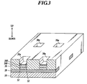
- FIG. 3 is a sectional view schematically showing a main part of the switching elements 1 in a course of manufacture when the lower-gap member forming step is completed.
- the holes 30a are formed in a predetermined interval, and the first electronic element 200, second electronic element 300 and lower-gap member 51 are formed inside each of the holes 30a.
- the switching element 1 and the memory element array comprising the switching elements 1 of the present embodiment comprise the insulative body 30, the first electrode 20 and second electrode 40 provided to the insulative body 30, the interelectrode gap 50 between the first electrode 20 and second electrode 40 which has a gap in a nanometer order that causes switching phenomenon of resistance by applying a predetermined voltage between the first electrode 20 and second electrode 40, and the sealing member 60 which seals the interelectrode gap 50 such that the gap is retained.
- the switching element 1 can be used under any atmosphere.
Landscapes
- Semiconductor Memories (AREA)
- Manufacture Of Switches (AREA)
Claims (4)
- Schaltelement, das umfasst:ein isolierendes Substrat (10);eine erste Elektrode (20) und eine zweite Elektrode (40), die an dem isolierenden Substrat (10) vorhanden sind, wobei die erste Elektrode (20) in Kontakt mit einer oberen Fläche des isolierenden Substrats (10) ist;einen Elektrodenzwischenraum (50) zwischen der ersten Elektrode (20) und der zweiten Elektrode (40), der einen Zwischenraum in einer Nanometer-Größenordnung umfasst, der einen Widerstands-Schaltvorgang durch Anlegen einer vorgegebenen Spannung zwischen der ersten Elektrode (20) und der zweiten Elektrode (40) bewirkt; undein Dichtungselement (60), das den Elektrodenzwischenraum (50) so abdichtet, dass der Zwischenraum aufrechterhalten wird;gekennzeichnet durcheinen isolierenden Körper (30), der die erste Elektrode (20) abdeckt,wobei der isolierende Körper (30) ein Loch (30a) enthält, das einen Teil einer oberen Fläche der ersten Elektrode (20) freilegt,die zweite Elektrode (40) über der ersten Elektrode (20) angeordnet ist,die zweite Elektrode (40) in Kontakt mit einer oberen Fläche des isolierenden Körpers (30) ist,der Elektrodenzwischenraum (50) innerhalb des Lochs (30a) vorhanden ist, unddas Dichtungselement (60) eine obere Fläche der zweiten Elektrode (40) sowie eine Öffnung des Lochs (30a) abdeckt.
- Schaltelement nach Anspruch 1, wobei das Dichtungselement (60) aus isolierendem Material besteht.
- Verfahren zum Herstellen eines Schaltelementes, das umfasst:einen Schritt zum Fertigen eines isolierenden Substrats, in dem ein isolierendes Substrat (10) gefertigt wird;einen Schritt zum Ausbilden einer ersten Elektrode, in dem eine erste Elektrode (20) an der oberen Fläche des isolierenden Substrats (10) ausgebildet wird;gekennzeichnet durcheinen Schritt zum Ausbilden eines isolierenden Körpers, in dem ein isolierender Körper (30) so ausgebildet wird, dass er die erste Elektrode (20) abdeckt, und in dem ein Loch (30a) in dem isolierenden Körper (30) ausgebildet wird, um einen Teil der oberen Fläche der ersten Elektrode (20) freizulegen;einen Schritt zum Ausbilden eines unteren Zwischenraumelementes, in dem ein unteres Zwischenraumelement (51) in der Innenwand des Lochs (30a) an der ersten Elektrode (20) ausgebildet wird;einen Schritt zum Ausbilden eines oberen Zwischenraumelementes sowie einer zweiten Elektrode, in dem ein oberes Zwischenraumelement (52) an der oberen Seite der Innenwand des Lochs (30a) ausgebildet wird, um einen Elektrodenzwischenraum (50) auszubilden, und eine zweite Elektrode (40) an der oberen Fläche des isolierenden Körpers (30) ausgebildet wird; undeinen Schritt zum Ausbilden eines Dichtungselementes, in dem ein Dichtungselement (60) so ausgebildet wird, dass es die obere Fläche der zweiten Elektrode (40) und die Öffnung des Lochs (30a) abdeckt.
- Speicherelementgruppe, die eine Vielzahl der Schaltelemente nach Anspruch 1 oder 2 umfasst, die in einer Gruppe (100) als Speicherelemente angeordnet sind, wobei die Elektrodenzwischenräume (50) der Schaltelemente mit dem Dichtungselement (60) separat und unabhängig voneinander abgedichtet sind.
Applications Claiming Priority (1)
| Application Number | Priority Date | Filing Date | Title |
|---|---|---|---|
| JP2007215864A JP2009049287A (ja) | 2007-08-22 | 2007-08-22 | スイッチング素子、スイッチング素子の製造方法及びメモリ素子アレイ |
Publications (3)
| Publication Number | Publication Date |
|---|---|
| EP2028693A2 EP2028693A2 (de) | 2009-02-25 |
| EP2028693A3 EP2028693A3 (de) | 2012-06-06 |
| EP2028693B1 true EP2028693B1 (de) | 2014-03-19 |
Family
ID=39951627
Family Applications (1)
| Application Number | Title | Priority Date | Filing Date |
|---|---|---|---|
| EP08014730.9A Not-in-force EP2028693B1 (de) | 2007-08-22 | 2008-08-19 | Schaltelement, Verfahren zur Herstellung des Schaltelements und Speicherelementmatrix |
Country Status (5)
| Country | Link |
|---|---|
| US (1) | US8045359B2 (de) |
| EP (1) | EP2028693B1 (de) |
| JP (1) | JP2009049287A (de) |
| KR (1) | KR101449916B1 (de) |
| CN (1) | CN101373787B (de) |
Families Citing this family (4)
| Publication number | Priority date | Publication date | Assignee | Title |
|---|---|---|---|---|
| JP4544340B2 (ja) | 2008-01-24 | 2010-09-15 | ソニー株式会社 | 電子素子およびその製造方法並びに記憶装置 |
| JP5455415B2 (ja) * | 2009-04-10 | 2014-03-26 | 株式会社船井電機新応用技術研究所 | ナノギャップ電極を有する素子の製造方法 |
| US9324422B2 (en) * | 2011-04-18 | 2016-04-26 | The Board Of Trustees Of The University Of Illinois | Adaptive resistive device and methods thereof |
| US9412442B2 (en) | 2012-04-27 | 2016-08-09 | The Board Of Trustees Of The University Of Illinois | Methods for forming a nanowire and apparatus thereof |
Family Cites Families (12)
| Publication number | Priority date | Publication date | Assignee | Title |
|---|---|---|---|---|
| FR2717308B1 (fr) | 1994-03-14 | 1996-07-26 | Sgs Thomson Microelectronics | Dispositif de protection contre des surtensions dans des circuits intégrés. |
| JP2713152B2 (ja) | 1994-03-30 | 1998-02-16 | 日本電気株式会社 | 単一電子トンネリング効果素子およびその製造方法 |
| JPH08242008A (ja) | 1995-03-03 | 1996-09-17 | Toshiba Corp | 微小トンネル接合デバイスとその製造方法 |
| JP3710880B2 (ja) | 1996-06-28 | 2005-10-26 | 株式会社東芝 | 不揮発性半導体記憶装置 |
| CN100448049C (zh) * | 2001-09-25 | 2008-12-31 | 独立行政法人科学技术振兴机构 | 使用固体电解质的电气元件和存储装置及其制造方法 |
| US6699779B2 (en) * | 2002-03-22 | 2004-03-02 | Hewlett-Packard Development Company, L.P. | Method for making nanoscale wires and gaps for switches and transistors |
| DE10256486A1 (de) * | 2002-12-03 | 2004-07-15 | Infineon Technologies Ag | Verfahren zum Herstellen einer Speicherzelle, Speicherzelle und Speicherzellen-Anordnung |
| JP3864229B2 (ja) | 2003-08-29 | 2006-12-27 | 独立行政法人産業技術総合研究所 | ナノギャップ電極の製造方法及び該方法により製造されたナノギャップ電極を有する素子 |
| JP4919146B2 (ja) * | 2005-09-27 | 2012-04-18 | 独立行政法人産業技術総合研究所 | スイッチング素子 |
| JP5297584B2 (ja) * | 2005-10-14 | 2013-09-25 | 株式会社半導体エネルギー研究所 | 半導体装置、半導体装置を用いた温度センサー及び半導体装置の作製方法 |
| JP5170615B2 (ja) * | 2007-03-26 | 2013-03-27 | 株式会社船井電機新応用技術研究所 | スイッチング素子 |
| JP5120874B2 (ja) * | 2007-06-22 | 2013-01-16 | 株式会社船井電機新応用技術研究所 | スイッチング素子 |
-
2007
- 2007-08-22 JP JP2007215864A patent/JP2009049287A/ja active Pending
-
2008
- 2008-08-12 KR KR1020080078890A patent/KR101449916B1/ko not_active Expired - Fee Related
- 2008-08-19 EP EP08014730.9A patent/EP2028693B1/de not_active Not-in-force
- 2008-08-20 US US12/195,165 patent/US8045359B2/en not_active Expired - Fee Related
- 2008-08-22 CN CN2008101445948A patent/CN101373787B/zh not_active Expired - Fee Related
Also Published As
| Publication number | Publication date |
|---|---|
| EP2028693A2 (de) | 2009-02-25 |
| US20090052223A1 (en) | 2009-02-26 |
| KR101449916B1 (ko) | 2014-10-15 |
| EP2028693A3 (de) | 2012-06-06 |
| US8045359B2 (en) | 2011-10-25 |
| JP2009049287A (ja) | 2009-03-05 |
| CN101373787A (zh) | 2009-02-25 |
| CN101373787B (zh) | 2012-07-04 |
| KR20090020486A (ko) | 2009-02-26 |
Similar Documents
| Publication | Publication Date | Title |
|---|---|---|
| CN101395717B (zh) | 电阻变化型元件、半导体装置、和其制造方法 | |
| EP3475989B1 (de) | Flexibles thermoelektrisches modul | |
| KR102047736B1 (ko) | 가요성 열전 모듈 | |
| US20080277646A1 (en) | Vertical Type Nanotube Semiconductor Device | |
| EP2006928B1 (de) | Schaltelement | |
| US20130037836A1 (en) | Light emitting device and method for fabricating the same | |
| US20120152299A1 (en) | Solar Cell And Solar Cell Module With Improved Read-Side Electrodes, And Production Method | |
| EP2028693B1 (de) | Schaltelement, Verfahren zur Herstellung des Schaltelements und Speicherelementmatrix | |
| EP1880420A1 (de) | Nanoröhrchen-geräte mit zwei anschlüssen sowie entsprechende systeme und herstellungsverfahren dafür | |
| KR102429968B1 (ko) | 광전자 장치 및 그 제조 방법 | |
| KR102414392B1 (ko) | 열전 테이프 | |
| WO2009064842A1 (en) | Vertically-stacked electronic devices having conductive carbon films | |
| CN103250247A (zh) | 用于光电子半导体芯片的载体和半导体芯片 | |
| US20090251199A1 (en) | Switching Element | |
| JP2008243986A (ja) | スイッチング素子 | |
| US20020008952A1 (en) | Electrostatic discharge device of surface mount type and fabricating method thereof | |
| JPH036675B2 (de) | ||
| US8653912B2 (en) | Switching element | |
| EP2006912B1 (de) | Speicherelementanordnung mit einem Schaltelement mit Nanohohlraum und einem Tunnelelement | |
| KR100946758B1 (ko) | 발광 다이오드 소자와 그 제조 방법 | |
| US6084245A (en) | Field emitter cell and array with vertical thin-film-edge emitter | |
| KR20090014327A (ko) | 보호 소자를 갖춘 발광소자 | |
| US7446014B2 (en) | Nanoelectrochemical cell | |
| CN101490879A (zh) | 金属膜包封 | |
| US8273584B2 (en) | Light emitting diode |
Legal Events
| Date | Code | Title | Description |
|---|---|---|---|
| PUAI | Public reference made under article 153(3) epc to a published international application that has entered the european phase |
Free format text: ORIGINAL CODE: 0009012 |
|
| AK | Designated contracting states |
Kind code of ref document: A2 Designated state(s): AT BE BG CH CY CZ DE DK EE ES FI FR GB GR HR HU IE IS IT LI LT LU LV MC MT NL NO PL PT RO SE SI SK TR |
|
| AX | Request for extension of the european patent |
Extension state: AL BA MK RS |
|
| PUAL | Search report despatched |
Free format text: ORIGINAL CODE: 0009013 |
|
| AK | Designated contracting states |
Kind code of ref document: A3 Designated state(s): AT BE BG CH CY CZ DE DK EE ES FI FR GB GR HR HU IE IS IT LI LT LU LV MC MT NL NO PL PT RO SE SI SK TR |
|
| AX | Request for extension of the european patent |
Extension state: AL BA MK RS |
|
| RIC1 | Information provided on ipc code assigned before grant |
Ipc: H01L 27/24 20060101AFI20120503BHEP Ipc: H01L 45/00 20060101ALI20120503BHEP |
|
| 17P | Request for examination filed |
Effective date: 20121205 |
|
| AKX | Designation fees paid |
Designated state(s): DE FR GB |
|
| GRAP | Despatch of communication of intention to grant a patent |
Free format text: ORIGINAL CODE: EPIDOSNIGR1 |
|
| INTG | Intention to grant announced |
Effective date: 20131002 |
|
| GRAS | Grant fee paid |
Free format text: ORIGINAL CODE: EPIDOSNIGR3 |
|
| GRAA | (expected) grant |
Free format text: ORIGINAL CODE: 0009210 |
|
| AK | Designated contracting states |
Kind code of ref document: B1 Designated state(s): DE FR GB |
|
| REG | Reference to a national code |
Ref country code: GB Ref legal event code: FG4D |
|
| REG | Reference to a national code |
Ref country code: DE Ref legal event code: R096 Ref document number: 602008030928 Country of ref document: DE Effective date: 20140430 |
|
| REG | Reference to a national code |
Ref country code: DE Ref legal event code: R097 Ref document number: 602008030928 Country of ref document: DE |
|
| PLBE | No opposition filed within time limit |
Free format text: ORIGINAL CODE: 0009261 |
|
| STAA | Information on the status of an ep patent application or granted ep patent |
Free format text: STATUS: NO OPPOSITION FILED WITHIN TIME LIMIT |
|
| 26N | No opposition filed |
Effective date: 20141222 |
|
| REG | Reference to a national code |
Ref country code: DE Ref legal event code: R097 Ref document number: 602008030928 Country of ref document: DE Effective date: 20141222 |
|
| REG | Reference to a national code |
Ref country code: DE Ref legal event code: R082 Ref document number: 602008030928 Country of ref document: DE Representative=s name: GRUENECKER PATENT- UND RECHTSANWAELTE PARTG MB, DE Ref country code: DE Ref legal event code: R081 Ref document number: 602008030928 Country of ref document: DE Owner name: FUNAI ELECTRIC CO., LTD., DAITO-SHI, JP Free format text: FORMER OWNER: FUNAI ELECTRIC ADVANCED APPLIED, FUNAI ELECTRIC CO., LTD., , JP Ref country code: DE Ref legal event code: R081 Ref document number: 602008030928 Country of ref document: DE Owner name: FUNAI ELECTRIC CO., LTD., DAITO-SHI, JP Free format text: FORMER OWNERS: FUNAI ELECTRIC ADVANCED APPLIED TECHNOLOGY RESEARCH INSTITUTE INC., TSUKUBA-SHI, IBARAKI, JP; FUNAI ELECTRIC CO., LTD., DAITO-SHI, OSAKA, JP |
|
| REG | Reference to a national code |
Ref country code: GB Ref legal event code: 732E Free format text: REGISTERED BETWEEN 20150611 AND 20150617 |
|
| REG | Reference to a national code |
Ref country code: FR Ref legal event code: TP Owner name: FUNAI ELECTRIC CO., LTD., JP Effective date: 20150917 Ref country code: FR Ref legal event code: CA Effective date: 20150917 |
|
| REG | Reference to a national code |
Ref country code: FR Ref legal event code: PLFP Year of fee payment: 9 |
|
| PGFP | Annual fee paid to national office [announced via postgrant information from national office to epo] |
Ref country code: GB Payment date: 20160817 Year of fee payment: 9 |
|
| PGFP | Annual fee paid to national office [announced via postgrant information from national office to epo] |
Ref country code: FR Payment date: 20160712 Year of fee payment: 9 |
|
| REG | Reference to a national code |
Ref country code: DE Ref legal event code: R084 Ref document number: 602008030928 Country of ref document: DE |
|
| GBPC | Gb: european patent ceased through non-payment of renewal fee |
Effective date: 20170819 |
|
| REG | Reference to a national code |
Ref country code: FR Ref legal event code: ST Effective date: 20180430 |
|
| PG25 | Lapsed in a contracting state [announced via postgrant information from national office to epo] |
Ref country code: GB Free format text: LAPSE BECAUSE OF NON-PAYMENT OF DUE FEES Effective date: 20170819 |
|
| PG25 | Lapsed in a contracting state [announced via postgrant information from national office to epo] |
Ref country code: FR Free format text: LAPSE BECAUSE OF NON-PAYMENT OF DUE FEES Effective date: 20170831 |
|
| PGFP | Annual fee paid to national office [announced via postgrant information from national office to epo] |
Ref country code: DE Payment date: 20210706 Year of fee payment: 14 |
|
| REG | Reference to a national code |
Ref country code: DE Ref legal event code: R079 Ref document number: 602008030928 Country of ref document: DE Free format text: PREVIOUS MAIN CLASS: H01L0027240000 Ipc: H10B0063000000 |
|
| REG | Reference to a national code |
Ref country code: DE Ref legal event code: R119 Ref document number: 602008030928 Country of ref document: DE |
|
| PG25 | Lapsed in a contracting state [announced via postgrant information from national office to epo] |
Ref country code: DE Free format text: LAPSE BECAUSE OF NON-PAYMENT OF DUE FEES Effective date: 20230301 |