EP2024909B1 - Mit sicherheitsfunktionen ausgestattetes elektronisches board und verfahren zur sicherstellung der sicherheit elektronischer boards - Google Patents
Mit sicherheitsfunktionen ausgestattetes elektronisches board und verfahren zur sicherstellung der sicherheit elektronischer boards Download PDFInfo
- Publication number
- EP2024909B1 EP2024909B1 EP07729846A EP07729846A EP2024909B1 EP 2024909 B1 EP2024909 B1 EP 2024909B1 EP 07729846 A EP07729846 A EP 07729846A EP 07729846 A EP07729846 A EP 07729846A EP 2024909 B1 EP2024909 B1 EP 2024909B1
- Authority
- EP
- European Patent Office
- Prior art keywords
- circuits
- electrical
- control circuit
- circuit
- signals
- Prior art date
- Legal status (The legal status is an assumption and is not a legal conclusion. Google has not performed a legal analysis and makes no representation as to the accuracy of the status listed.)
- Ceased
Links
Images


Classifications
-
- G—PHYSICS
- G06—COMPUTING OR CALCULATING; COUNTING
- G06K—GRAPHICAL DATA READING; PRESENTATION OF DATA; RECORD CARRIERS; HANDLING RECORD CARRIERS
- G06K19/00—Record carriers for use with machines and with at least a part designed to carry digital markings
- G06K19/06—Record carriers for use with machines and with at least a part designed to carry digital markings characterised by the kind of the digital marking, e.g. shape, nature, code
- G06K19/067—Record carriers with conductive marks, printed circuits or semiconductor circuit elements, e.g. credit or identity cards also with resonating or responding marks without active components
- G06K19/07—Record carriers with conductive marks, printed circuits or semiconductor circuit elements, e.g. credit or identity cards also with resonating or responding marks without active components with integrated circuit chips
- G06K19/073—Special arrangements for circuits, e.g. for protecting identification code in memory
- G06K19/07309—Means for preventing undesired reading or writing from or onto record carriers
- G06K19/07345—Means for preventing undesired reading or writing from or onto record carriers by activating or deactivating at least a part of the circuit on the record carrier, e.g. ON/OFF switches
-
- G—PHYSICS
- G06—COMPUTING OR CALCULATING; COUNTING
- G06K—GRAPHICAL DATA READING; PRESENTATION OF DATA; RECORD CARRIERS; HANDLING RECORD CARRIERS
- G06K19/00—Record carriers for use with machines and with at least a part designed to carry digital markings
- G06K19/06—Record carriers for use with machines and with at least a part designed to carry digital markings characterised by the kind of the digital marking, e.g. shape, nature, code
- G06K19/067—Record carriers with conductive marks, printed circuits or semiconductor circuit elements, e.g. credit or identity cards also with resonating or responding marks without active components
- G06K19/07—Record carriers with conductive marks, printed circuits or semiconductor circuit elements, e.g. credit or identity cards also with resonating or responding marks without active components with integrated circuit chips
- G06K19/073—Special arrangements for circuits, e.g. for protecting identification code in memory
-
- G—PHYSICS
- G06—COMPUTING OR CALCULATING; COUNTING
- G06F—ELECTRIC DIGITAL DATA PROCESSING
- G06F21/00—Security arrangements for protecting computers, components thereof, programs or data against unauthorised activity
-
- G—PHYSICS
- G06—COMPUTING OR CALCULATING; COUNTING
- G06K—GRAPHICAL DATA READING; PRESENTATION OF DATA; RECORD CARRIERS; HANDLING RECORD CARRIERS
- G06K19/00—Record carriers for use with machines and with at least a part designed to carry digital markings
- G06K19/06—Record carriers for use with machines and with at least a part designed to carry digital markings characterised by the kind of the digital marking, e.g. shape, nature, code
- G06K19/067—Record carriers with conductive marks, printed circuits or semiconductor circuit elements, e.g. credit or identity cards also with resonating or responding marks without active components
- G06K19/07—Record carriers with conductive marks, printed circuits or semiconductor circuit elements, e.g. credit or identity cards also with resonating or responding marks without active components with integrated circuit chips
- G06K19/073—Special arrangements for circuits, e.g. for protecting identification code in memory
- G06K19/07309—Means for preventing undesired reading or writing from or onto record carriers
-
- G—PHYSICS
- G06—COMPUTING OR CALCULATING; COUNTING
- G06K—GRAPHICAL DATA READING; PRESENTATION OF DATA; RECORD CARRIERS; HANDLING RECORD CARRIERS
- G06K7/00—Methods or arrangements for sensing record carriers, e.g. for reading patterns
- G06K7/0013—Methods or arrangements for sensing record carriers, e.g. for reading patterns by galvanic contacts, e.g. card connectors for ISO-7816 compliant smart cards or memory cards, e.g. SD card readers
- G06K7/0086—Methods or arrangements for sensing record carriers, e.g. for reading patterns by galvanic contacts, e.g. card connectors for ISO-7816 compliant smart cards or memory cards, e.g. SD card readers the connector comprising a circuit for steering the operations of the card connector
- G06K7/0091—Methods or arrangements for sensing record carriers, e.g. for reading patterns by galvanic contacts, e.g. card connectors for ISO-7816 compliant smart cards or memory cards, e.g. SD card readers the connector comprising a circuit for steering the operations of the card connector the circuit comprising an arrangement for avoiding intrusions and unwanted access to data inside of the connector
Definitions
- the present invention relates to an electronic card with security functions and a method for securing the electronic card.
- Electrical appliances contain one or more printed circuits to which electronic components are attached.
- the printed circuits are provided with several layers of copper strips thus ensuring the electrical connections, the width of the copper strips being typically of 0.3 millimeters .
- the most common technique is through holes. The printed circuit is holed and metallization is performed in the hole to electrically connect all the copper strips through which the hole passes.
- Some devices have security features. These devices include: banking equipment, control boxes for access to premises or computers, control devices for dangerous equipment (radiological machines, weapons controls, locking of military devices, etc.) , devices comprising security modules for generating keys or signatures using cryptographic calculation, television decoders, etc. These devices generally allow access to data when security codes are presented correctly. The verification of these security codes is performed using keys stored in a memory of a component. Much of the security of the system comes from the fact that these keys can not be read outside a secure enclosure. To protect access to the memory containing sensitive data, a first method is to embed all the components and the circuit board in a resin or polymerized glue. Connectors attached to the resin block allow the communication, including the introduction of access codes.
- the central unit the non-volatile memory
- the cryptoprocessor the data to be secured are usually exchanged via a communication bus.
- a large number of circuits receive and / or transmit data on this bus and do not necessarily have security functions.
- these circuits receive on the bus the same data to secure, so they must also be spaced from each other by at most 3 millimeters.
- the document FR 2,857,534 filed by INNOVA CARD describes an integrated circuit comprising an ordinary module and a secure module connected to one another by a protected link.
- the requests transmitted to the secure module circulate in clear on the ordinary bus and are encrypted on the secure bus.
- the modules include master and slave elements.
- the request from a master element is encrypted by its scrambling module before being transmitted to a slave element. It is then decrypted by a protection module which routes it to the slave element.
- This document does not describe solutions to limit the probing (in English "probing") of signals by electrical conductors applied to the printed circuit.
- Our invention makes it possible, among other things, to limit the implementation constraints of the integrated circuits while ensuring a high level of security to certain areas of the printed circuit.
- the invention relates to an electronic card comprising a so-called secure zone comprising a plurality of first electronic circuits including a control circuit, said first circuits being separated from each other by at most a determined distance, the electrical connections connected to the first circuits and transmitting secure signals not moving away from said first circuits by at most said determined distance, and an unsecured area comprising second electronic circuits which are distant from the first circuits by more than the determined distance or whose electrical links are transmitting signals secure are distant more than said determined distance; characterized in that the secure area comprises a communication circuit for passing signals between the first and second circuits, the passage of the electrical signals in the communication circuit being conditioned by an electrical control signal emitted by the control circuit.
- several communication circuits receive the same electrical control signal emitted by the control circuit.
- relatively common circuits can be used and arranged on the electronic board to have the necessary number to secure all the signals.
- part of the signals exchanged between the first and second circuits pass through the communication circuit, the signals not crossing the circuit being considered as unsecured. In this way, the number and size of the communication circuit are optimized.
- the electrical control signal conditioning the passage of electrical signals in the circuit of communication is a function of the operating code of the instruction being executed in the control circuit.
- the electrical control signal is a function of the address of the operating code of the instruction being executed in the control circuit. In this way, one can compartmentalize program code banks and assign them a security criterion.
- the electrical control signal is emitted by an output port of the control circuit. One can thus use a very common circuit and use a port to fix by an electrical level the safe state or not instructions that will then be executed.
- the electrical control signal is connected to an input port of the control circuit so as to read its electrical state present on the electronic card.
- the control circuit blocks if the physically detected state at the input port does not match the logic state imposed by the control circuit. In this way, if an attempt is made to force the electrical control signal to an inactive state, it can be detected and, if necessary, blocked the operation of the control circuit.
- the communication circuit contains a memory allowing the control circuit to save data. In this way, the communication circuit and the memory are only one circuit, so there is one less circuit to integrate in the secure area.
- the present invention also relates to a method for controlling access to data within an electronic card comprising a so-called secure zone comprising a plurality of first electronic circuits including a control circuit, said first circuits being distant from each other. at most a determined distance, the electrical connections connected to the first circuits and transmitting secure signals not moving away from said first circuits by at most said determined distance, and an insecure zone comprising second electronic circuits which are distant from the first circuits of more than the specified distance or whose links electrical transmitters transmitting secure signals are further apart from said determined distance; characterized in that the secure area comprises a communication circuit for passing signals between the first and second circuits, the passage of the electrical signals in the communication circuit being conditioned by an electrical control signal transmitted by the control circuit, the method comprising a step of reading the electrical control signal by the control circuit so as to read its electrical state, and a step of blocking said control circuit if the detected electrical state does not correspond to the state imposed by the control circuit.
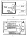
- the electronic card is implemented in a receiver as represented in FIG. figure 1 , typically a decoder associated with a display device 2.
- the receiver comprises a central unit 3 connected to a program memory 6, an infrared signal receiver 7 for receiving the signals of a remote control, interface circuits 5 for example the data display on the front panel and an audio decoding logic / video 9 for the generation of audiovisual signals sent to the television screen 2.
- the receiver 1 also comprises a circuit 8 for displaying data on the screen, often called OSD circuit, of the English "On Screen Display” ( meaning literally "on-screen display”).
- the OSD circuit 8 is a text and graphics generator that makes it possible to display menus, pictograms or other graphics on the screen.
- the receiver has a connector allowing in particular to receive audio and / or video data from a broadcast network through a receiving antenna associated with a demodulator 4, this network can be of radio, cable or satellite type.
- the connectors also provide communication with a high-speed local digital bus for receiving information about broadcast audio.
- Interface 5 also allows other devices to be connected, eg devices with USB, CVBS (composite video input) or 4: 2: 2 (CCIR 656 - digital video) connections, through other connectors .
- the electronic card may for example be arranged in banking devices, control boxes for access to premises or computers, devices for controlling dangerous equipment, devices comprising security modules for generating keys or keys. signature using cryptographic computation, television decoders, etc.
- the figure 2 shows a block diagram of the printed circuit 2.1 schematically showing the circuits to be secured and the circuits that do not need to be.
- the circuits to be secured are grouped on an area of the printed circuit, thus defining a secure area.
- These circuits respect the rule of 3 millimeters, that is to say they are not distant from each other by more than 3 millimeters and the tracks carrying signals to be secured between the circuits of the secure zone do not move away. no longer from this distance.
- there is typically a control unit 2.2 which in some cases can be the central unit 3 globally managing the receiver 1 and a non-volatile memory 2.3 for storing the executable code and secret data.
- the other 2.4 circuits do not need to be so close provided they do not receive secure signals.
- the secure zone is equipped with a "logic bus circuit with isolated output” 2.5 or “buffer” in English.
- the transmitter circuit 2.5 performs a gate function for exchanging signals between a secure area of the card and the rest of the electrical circuits.
- this gate is a bidirectional amplifier (or "Buffer” in English), for example a circuit referenced 74LVCR2245APW.
- This circuit has two control inputs: the input DIR (not shown) defines the direction of the data, it is connected to the control circuit 2.2 which defines at any time the direction of transmission of the data of the bus.
- the input OE (of the English "Output Enable") or not the output of the transmitter circuit 2.5, that is to say if this input is not activated, the outputs are in three-state logic and it n It is not possible then to read the data placed in inputs. If the OE input is activated, then the outputs reproduce exactly the signals placed on the different input lines of the transmitter circuit 2.5.
- the input OE is connected by a wire 2.6 to the control unit 2.2. It should be noted that the set of circuits 2.2, 2.3 and 2.5 must obey the rule of 3 millimeters.
- the figure 3 is a diagram showing the main circuits of the secure area with their main links.
- the interface circuit marked "PERIPHERAL TSOP” does not belong to the secure zone. It shows that it is connected to the control circuit marked "CPU BGA” by lines passing the 74LVCR2245APW transmitters circuit and by direct lines, the latter being unsecured.
- the figure 4 represents an implementation drawing of the main circuits of the secure zone according to the example of implementation of the realized prototype. We see in particular the application of the rule of 3 millimeters.
- the logic state of the control wire 2.6 of the transmitting circuit 2.5 depends on whether the instruction currently executed by the control circuit 2.2 is secure or not.
- This circuit has two sets of instructions identified by operating codes, any instruction of the safe instruction set triggers the activation of the transmitter circuit 2.5 via the wire 2.6.
- the execution of an unsafe game instruction does not trigger activation of the transmitter circuit 2.5.
- One variant consists in that the control circuit 2.2 updates the logic state of the control wire 2.6 as a function of the memory address of the instruction to be executed.
- a simple way is to share the program memory in the bank and assign each bank an indicator specifying the security character. When a bank is marked as "secure,” any statement execution stored in this bank activates the 2.6 control thread. to the transmitter circuit 2.5.
- the indicator is in an integrated EEPROM memory in the control circuit 2.2, its initialization is done in personalization mode of the component and after presentation of an access code.
- a third variant consists in that the control wire 2.6 of the transmitter circuit 2.5 is connected to an output pin of an I / O port of the control circuit 2.2.
- the control circuit 2.2 Before executing an executable code routine, the control circuit 2.2 initializes with an instruction the value of the bit enabling activation of the wire 2.6. At the end of the routine, by another instruction, the control circuit 2.2 deactivates the wire.
- the control circuit 2.2 has an input circuit making it possible to read the electrical state of the wire 2.6.
- This improvement is particularly useful in the case where a malefactor has managed to impose on this wire an inactive state, which would leave open the gate consisting of the transmitter circuit 2.5 and thus allow to see secure signals.
- the executable program can thus check whether the control of the logical state of the wire 2.6 corresponds to its electrical level. If the program detects an electrical level corresponding to a deactivation while its command activates it, it locks itself up and refrains from performing any security functions. Blocking may consist of burning a fuse inside the control circuit. During subsequent power-up, the control unit 2.2 tests the state of the fuse and interrupts its operation if the fuse is blown. Another way to do this is to write the information corresponding to the state of a fuse in an EEPROM cell in a memory internal or external to the control unit 2.2.
- the memory 2.3 is integrated in the transmitter circuit 2.5.
- the figure 5 shows a block diagram of the printed circuit 2.1 schematically showing the circuits to be secured and the circuits that do not need to be.
- the memory 3.1 then has a direct access port for the data bus, the address bus and the control signals, and a secondary port for the signal inputs and outputs to the unsecured portion of the printed circuit.
- the secondary port is seen by the control circuit 2.2 as a part of the memory, having a predetermined number of memory words, the memory word having a number of data bits.
- the secondary port has 8 address lines, 8 data lines, and control signals such as "R / W" and "VMA,” meaning the meaning of the data and the fact that the configuration of the address signals is valid on the secondary port.
- the secondary port is seen by the control circuit 2.2 as a 256-byte memory.
- the communication circuit (2.5) stores data and does not allow the transmission of this data in the secure part when the control electric signal (2.6) is activated. In this way, when the information is sensitive, it remains in the memory of the secure part and is not readable by the electronic circuits of the unsecured part.
- the figure 6 is a diagram of the main circuits of the secure area with their main links according to the other embodiment.
- the non-volatile memory comprises a "FLASH BGA" type memory and at least one 74LVCR2245APW transmitter circuit. We see in comparison with the figure 3 that the number of links has decreased. Due to the integration of the transmitter circuit and the memory into a single circuit, the size of the secure area is reduced.
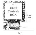
- the figure 7 represents an implementation drawing of the main circuits of the secure zone according to the other embodiment described by the figure 4 .
- switching from three two-circuit circuits reduces the space occupied by the secure environment on the circuit board.
Landscapes
- Engineering & Computer Science (AREA)
- Computer Hardware Design (AREA)
- Theoretical Computer Science (AREA)
- Physics & Mathematics (AREA)
- General Physics & Mathematics (AREA)
- Computer Security & Cryptography (AREA)
- General Engineering & Computer Science (AREA)
- Microelectronics & Electronic Packaging (AREA)
- Artificial Intelligence (AREA)
- Computer Vision & Pattern Recognition (AREA)
- Software Systems (AREA)
- Storage Device Security (AREA)
Claims (10)
- Elektronische Platine (2.1) mit einem so genannten gesicherten Bereich mit einer Vielzahl erster elektronischer Schaltkreise (2.2, 2.3, 2.5), darunter einem Kontrollschaltkreis (2.2), wobei die ersten Schaltkreise um maximal einen bestimmten Abstand voneinander entfernt sind, wobei die elektrischen, mit den ersten Schaltkreisen (2.2, 2.3, 2.5) verbundenen und gesicherte Signale übertragenden Leitungen sich von den ersten Schaltkreisen nicht um mehr als um den bestimmten Abstand entfernen, und einem nicht gesicherten Bereich, der zweite elektronische Schaltkreise (2.4) umfasst, die von den ersten Schaltkreisen (2.2, 2.3, 2.5) um mehr als den bestimmten Abstand entfernt sind oder deren gesicherte Signale übertragende elektrische Leitungen um mehr als den bestimmten Abstand beabstandet sind, dadurch gekennzeichnet, dass der gesicherte Bereich einen Kommunikationsschaltkreis (2.5) umfasst, der den Übergang von Signalen zwischen den ersten und den zweiten Schaltkreisen ermöglicht, wobei der Übergang der elektrischen Signale in dem Kommunikationsschaltkreis (2.5) durch ein elektrisches Steuersignal (2.6) geregelt ist, das von dem Kontrollschaltkreis (2.2) ausgegeben wird.
- Elektronische Platine nach Anspruch 1, dadurch gekennzeichnet, dass das elektrische Steuersignal (2.6), das den Übergang der elektrischen Signale in dem Kommunikationsschaltkreis (2.5) regelt, von dem Operationscode der in dem Kontrollschaltkreis (2.2) in Ausführung befindlichen Anweisung abhängt.
- Elektronische Platine nach einem der Ansprüche 1 und 2, dadurch gekennzeichnet, dass das elektrische Steuersignal (2.6), das den Übergang der elektrischen Signale in dem Kommunikationsschaltkreis (2.5) regelt, von der Adresse des Operationscodes der in dem Kontrollschaltkreis (2.2) in Ausführung befindlichen Anweisung abhängt.
- Elektronische Platine nach einem der Ansprüche 1 bis 3, dadurch gekennzeichnet, dass das elektrische Steuersignal (2.6), das den Übergang der elektrischen Signale in dem Kommunikationsschaltkreis (2.5) regelt, von einem Ausgangsport des Kontrollschaltkreises (2.2) ausgegeben wird.
- Elektronische Platine nach einem der vorstehenden Ansprüche, dadurch gekennzeichnet, dass das elektrische Steuersignal (2.6) mit einem Eingangsport des Kontrollschaltkreises (2.2) derart verbunden ist, dass sein elektrischer Zustand abgelesen werden kann, wobei der Kontrollschaltkreis (2.2) sich verriegelt, wenn der am Port vorhandene Zustand dem von dem Kontrollschaltkreis (2.2) erforderten logischen Zustand nicht entspricht.
- Elektronische Platine nach einem der vorstehenden Ansprüche, dadurch gekennzeichnet, dass der Kommunikationsschaltkreis (2.5) einen Speicher umfasst, der es dem Kontrollschaltkreis (2.2) ermöglicht, Daten abzuspeichern, wenn das elektrische Steuersignal (2.6) aktiviert ist, durch das die Ausgabe der Daten zu dem nicht gesicherten Bereich somit blockiert wird.
- Verfahren für die Kontrolle des Datenzugangs innerhalb einer elektronischen Platine (2.1) mit einem so genannten gesicherten Bereich mit einer Vielzahl erster elektronischer Schaltkreise (2.2, 2.3, 2.5), darunter einem Kontrollschaltkreis (2.2), wobei die ersten Schaltkreise um maximal einen bestimmten Abstand voneinander entfernt sind, wobei die elektrischen, mit den ersten Schaltkreisen (2.2, 2.3, 2.5) verbundenen und gesicherte Signale übertragenden Leitungen sich von den ersten Schaltkreisen nicht um mehr als um den bestimmten Abstand entfernen, und einem nicht gesicherten Bereich, der zweite elektronische Schaltkreise (2.4) umfasst, die von den ersten Schaltkreisen (2.2, 2.3, 2.5) um mehr als den bestimmten Abstand entfernt sind oder deren gesicherte Signale übertragende elektrische Leitungen um mehr als den bestimmten Abstand beabstandet sind, dadurch gekennzeichnet, dass der gesicherte Bereich einen Kommunikationsschaltkreis (2.5) umfasst, der den Übergang von Signalen zwischen den ersten und den zweiten Schaltkreisen ermöglicht, wobei der Übergang der elektrischen Signale in dem Kommunikationsschaltkreis (2.5) durch ein elektrisches Steuersignal (2.6) geregelt ist, das von dem Kontrollschaltkreis (2.2) ausgegeben wird, wobei das Verfahren einen Schritt des Lesens des elektrischen Steuersignals (2.6) durch den Kontrollschaltkreis (2.2) aufweist, so dass dessen elektrischer Zustand abgelesen werden kann, und einen Schritt der Verriegelung des Kontrollschaltkreises (2.2), wenn der ermittelte elektrische Zustand dem von dem Kontrollschaltkreis erforderten Zustand nicht entspricht.
- Verfahren für die Kontrolle des Datenzugangs nach Anspruch 7, dadurch gekennzeichnet, dass der Zustand des elektrischen Steuersignals von dem Operationscode der in dem Kontrollschaltkreis (2.2) in Ausführung befindlichen Anweisung abhängt.
- Verfahren für die Kontrolle des Datenzugangs nach Anspruch 7, dadurch gekennzeichnet, dass der Zustand des elektrischen Steuersignals von der Adresse des Operationscodes der in dem Kontrollschaltkreis (2.2) in Ausführung befindlichen Anweisung abhängt.
- Verfahren für die Kontrolle des Datenzugangs nach einem der Ansprüche 7 bis 9, dadurch gekennzeichnet, dass es einen Schritt des Speicherns in dem Datenkommunikationsschaltkreis (2.5) umfasst, wenn das elektrische Steuersignal (2.6) aktiviert ist, durch das die Ausgabe der Daten zu dem nicht gesicherten Bereich somit blockiert wird.
Applications Claiming Priority (2)
| Application Number | Priority Date | Filing Date | Title |
|---|---|---|---|
| FR0652064A FR2902213B1 (fr) | 2006-06-08 | 2006-06-08 | Carte electronique dotee de fonctions securitaires |
| PCT/EP2007/055458 WO2007141233A1 (fr) | 2006-06-08 | 2007-06-04 | Carte electronique dotee de fonctions securitaires et procede de securisation de la carte electronique |
Publications (2)
| Publication Number | Publication Date |
|---|---|
| EP2024909A1 EP2024909A1 (de) | 2009-02-18 |
| EP2024909B1 true EP2024909B1 (de) | 2010-08-04 |
Family
ID=37744086
Family Applications (1)
| Application Number | Title | Priority Date | Filing Date |
|---|---|---|---|
| EP07729846A Ceased EP2024909B1 (de) | 2006-06-08 | 2007-06-04 | Mit sicherheitsfunktionen ausgestattetes elektronisches board und verfahren zur sicherstellung der sicherheit elektronischer boards |
Country Status (8)
| Country | Link |
|---|---|
| US (1) | US8499332B2 (de) |
| EP (1) | EP2024909B1 (de) |
| JP (1) | JP4920748B2 (de) |
| KR (1) | KR101287480B1 (de) |
| CN (1) | CN101479746B (de) |
| DE (1) | DE602007008233D1 (de) |
| FR (1) | FR2902213B1 (de) |
| WO (1) | WO2007141233A1 (de) |
Families Citing this family (2)
| Publication number | Priority date | Publication date | Assignee | Title |
|---|---|---|---|---|
| TW201227391A (en) * | 2010-12-16 | 2012-07-01 | Walton Advanced Eng Inc | Storage device with a hidden space and its operation method |
| JP2014038408A (ja) | 2012-08-13 | 2014-02-27 | International Business Maschines Corporation | 同時マルチスレッディング機能をもったプロセッサのパイプラインにおけるストール削減方法、削減装置及び削減プログラム |
Family Cites Families (23)
| Publication number | Priority date | Publication date | Assignee | Title |
|---|---|---|---|---|
| US4860351A (en) * | 1986-11-05 | 1989-08-22 | Ibm Corporation | Tamper-resistant packaging for protection of information stored in electronic circuitry |
| JPH07272398A (ja) * | 1994-03-28 | 1995-10-20 | Hitachi Ltd | ディスク装置の制御装置 |
| US5861662A (en) * | 1997-02-24 | 1999-01-19 | General Instrument Corporation | Anti-tamper bond wire shield for an integrated circuit |
| JPH1165937A (ja) * | 1997-08-25 | 1999-03-09 | Mitsubishi Electric Corp | Icメモリカード |
| US6708273B1 (en) * | 1997-09-16 | 2004-03-16 | Safenet, Inc. | Apparatus and method for implementing IPSEC transforms within an integrated circuit |
| US6704871B1 (en) * | 1997-09-16 | 2004-03-09 | Safenet, Inc. | Cryptographic co-processor |
| JPH11258293A (ja) * | 1998-03-16 | 1999-09-24 | Fujitsu Ltd | プリント配線板電気試験装置 |
| US6553496B1 (en) * | 1999-02-01 | 2003-04-22 | Koninklijke Philips Electronics N.V. | Integration of security modules on an integrated circuit |
| JP3822768B2 (ja) * | 1999-12-03 | 2006-09-20 | 株式会社ルネサステクノロジ | Icカードの製造方法 |
| US6418552B1 (en) * | 1999-12-10 | 2002-07-09 | Hewlett-Packard Company | Method and apparatus for optimizing trace lengths to maximize the speed of a clocked bus |
| US20030212897A1 (en) * | 2001-08-18 | 2003-11-13 | Russell Dickerson | Method and system for maintaining secure semiconductor device areas |
| CN1292356C (zh) * | 2002-04-17 | 2006-12-27 | 松下电器产业株式会社 | 非易失性半导体存储装置及其机密保护方法 |
| US7469420B2 (en) * | 2002-05-21 | 2008-12-23 | Thomson Licensing | Key transport tamper protection |
| EP1795992B1 (de) * | 2002-07-30 | 2018-01-24 | Fujitsu Limited | Verfahren und Gerät zur Wiedergabe von Information mit einem Sicherheitsmodul |
| US7181572B2 (en) * | 2002-12-02 | 2007-02-20 | Silverbrook Research Pty Ltd | Cache updating method and apparatus |
| FR2857534B1 (fr) * | 2003-07-09 | 2005-10-28 | Innova Card | Circuit integre comportant un module ordinaire et un module securise raccordes par une liaison protegee |
| US7627345B2 (en) * | 2003-09-09 | 2009-12-01 | Cinterion Wireless Modules Gmbh | Circuit arrangement that functions as an interface between a SIM card and GSM modem |
| JP2005250538A (ja) * | 2004-03-01 | 2005-09-15 | Kawasaki Microelectronics Kk | デバイス間通信装置 |
| US7644289B2 (en) * | 2004-03-23 | 2010-01-05 | Harris Corporation | Modular cryptographic device providing enhanced communication control features and related methods |
| TW200538001A (en) | 2004-05-14 | 2005-11-16 | Hon Hai Prec Ind Co Ltd | System and method for verifying space of the pcb layout nets |
| KR20070060101A (ko) * | 2004-08-30 | 2007-06-12 | 실리콘 스토리지 테크놀로지 인크 | 무선 단말기에서의 비휘발성 메모리 관리 시스템 및 방법 |
| JP2006127679A (ja) * | 2004-10-29 | 2006-05-18 | Toshiba Corp | 光ディスク装置及び光ディスク再生方法 |
| US7549064B2 (en) * | 2005-05-10 | 2009-06-16 | Hewlett-Packard Development Company, L.P. | Secure circuit assembly |
-
2006
- 2006-06-08 FR FR0652064A patent/FR2902213B1/fr not_active Expired - Fee Related
-
2007
- 2007-06-04 WO PCT/EP2007/055458 patent/WO2007141233A1/fr not_active Ceased
- 2007-06-04 KR KR1020087028945A patent/KR101287480B1/ko not_active Expired - Fee Related
- 2007-06-04 CN CN200780020620XA patent/CN101479746B/zh not_active Expired - Fee Related
- 2007-06-04 EP EP07729846A patent/EP2024909B1/de not_active Ceased
- 2007-06-04 JP JP2009513662A patent/JP4920748B2/ja not_active Expired - Fee Related
- 2007-06-04 DE DE602007008233T patent/DE602007008233D1/de active Active
- 2007-06-04 US US12/308,022 patent/US8499332B2/en not_active Expired - Fee Related
Also Published As
| Publication number | Publication date |
|---|---|
| JP2009540410A (ja) | 2009-11-19 |
| DE602007008233D1 (de) | 2010-09-16 |
| FR2902213A1 (fr) | 2007-12-14 |
| US8499332B2 (en) | 2013-07-30 |
| CN101479746B (zh) | 2012-07-25 |
| KR20090017542A (ko) | 2009-02-18 |
| WO2007141233A1 (fr) | 2007-12-13 |
| JP4920748B2 (ja) | 2012-04-18 |
| KR101287480B1 (ko) | 2013-07-19 |
| FR2902213B1 (fr) | 2008-10-17 |
| US20100017852A1 (en) | 2010-01-21 |
| EP2024909A1 (de) | 2009-02-18 |
| CN101479746A (zh) | 2009-07-08 |
Similar Documents
| Publication | Publication Date | Title |
|---|---|---|
| FR2948795A1 (fr) | Detecteur d'injection de fautes dans un circuit integre | |
| FR2711833A1 (fr) | Circuit intégré contenant une mémoire protégée et système sécurisé utilisant ledit circuit intégré. | |
| EP0252850A1 (de) | Verfahren zum Beglaubigen der Echtheit von Daten, ausgetauscht durch zwei Vorrichtungen, die örtlich oder entfernt mittels einer Übertragungsleitung verbunden sind | |
| EP0426541A1 (de) | Verfahren zum Schutz gegen betrügerischen Gebrauch einer Mikroprozessor-Karte und Vorrichtung zur Durchführung | |
| EP2024909B1 (de) | Mit sicherheitsfunktionen ausgestattetes elektronisches board und verfahren zur sicherstellung der sicherheit elektronischer boards | |
| FR2673016A1 (fr) | Procede de protection d'un circuit integre contre les utilisations frauduleuses. | |
| EP3586258A1 (de) | Segmentiertes schlüsselauthentifikationssystem | |
| EP3132403B1 (de) | Vorrichtung zur verarbeitung von daten aus einer kontaktlosen chipkarte, verfahren und entsprechendes computerprogramm | |
| EP3244375A1 (de) | Mikrocontroller zum gesicherten starten mit firewall | |
| FR2857113A1 (fr) | Boitier securise renfermant un clavier permettant d'introduire des donnees confidentielles | |
| WO1989003081A1 (fr) | Dispositif de protection des zones memoire d'un systeme electronique a microprocesseur | |
| EP1955248B1 (de) | Lernfähiges sicherheitsmodul | |
| EP2466506A1 (de) | Dynamisches Verfahren zur Überwachung der vollständigen Ausführung eines ausführbaren Codes | |
| FR3067192B1 (fr) | Appareil electronique comportant deux memoires et procede d'appairage associe | |
| FR2889005A1 (fr) | Integrite materielle permanente des donnees | |
| EP1952297A2 (de) | Verfahren und einrichtung zur authentifikation durch einen benutzer einer vertrauenswürdigen schnittstelle und diesbezügliches computerprogramm | |
| FR2619941A1 (fr) | Systeme de controle de la liaison entre deux terminaux d'une installation de traitement de donnees | |
| EP2343663A1 (de) | Verfahren zum polymorphen Schutz eines ausführbaren Codes | |
| EP1502234B1 (de) | Datenübertragungsverfahren zwischen einer chipkarte und einem benutzer, kartenlesegerät und karte zur durchführung des verfahrens | |
| EP1129430B2 (de) | Verfahren und gerät zur überprüfung des betriebszyklus eines tragbaren gegenstandes, insbesondere einer chipkarte | |
| BE1024111B1 (fr) | Microcontroleur pour demarrage securise avec pare-feu | |
| FR3003058A1 (fr) | Systeme et procede de gestion d’au moins une application en ligne, objet portable utilisateur usb et dispositif distant du systeme | |
| EP2280380A1 (de) | Personalisierungsverfahren einer elektronischen Einheit, und elektronische Einheit, die dieses Verfahren umsetzt | |
| FR2909466A1 (fr) | Procede et dispositif de memorisation securisee de donnees dans une memoire permanente de type a adressage par blocs |
Legal Events
| Date | Code | Title | Description |
|---|---|---|---|
| PUAI | Public reference made under article 153(3) epc to a published international application that has entered the european phase |
Free format text: ORIGINAL CODE: 0009012 |
|
| 17P | Request for examination filed |
Effective date: 20081204 |
|
| AK | Designated contracting states |
Kind code of ref document: A1 Designated state(s): AT BE BG CH CY CZ DE DK EE ES FI FR GB GR HU IE IS IT LI LT LU LV MC MT NL PL PT RO SE SI SK TR |
|
| AX | Request for extension of the european patent |
Extension state: AL BA HR MK RS |
|
| DAX | Request for extension of the european patent (deleted) | ||
| RBV | Designated contracting states (corrected) |
Designated state(s): DE FR GB |
|
| 17Q | First examination report despatched |
Effective date: 20090710 |
|
| GRAP | Despatch of communication of intention to grant a patent |
Free format text: ORIGINAL CODE: EPIDOSNIGR1 |
|
| RAP1 | Party data changed (applicant data changed or rights of an application transferred) |
Owner name: THOMSON LICENSING |
|
| GRAS | Grant fee paid |
Free format text: ORIGINAL CODE: EPIDOSNIGR3 |
|
| GRAA | (expected) grant |
Free format text: ORIGINAL CODE: 0009210 |
|
| AK | Designated contracting states |
Kind code of ref document: B1 Designated state(s): DE FR GB |
|
| REG | Reference to a national code |
Ref country code: GB Ref legal event code: FG4D Free format text: NOT ENGLISH |
|
| REF | Corresponds to: |
Ref document number: 602007008233 Country of ref document: DE Date of ref document: 20100916 Kind code of ref document: P |
|
| REG | Reference to a national code |
Ref country code: GB Ref legal event code: 746 Effective date: 20110302 |
|
| PLBE | No opposition filed within time limit |
Free format text: ORIGINAL CODE: 0009261 |
|
| STAA | Information on the status of an ep patent application or granted ep patent |
Free format text: STATUS: NO OPPOSITION FILED WITHIN TIME LIMIT |
|
| 26N | No opposition filed |
Effective date: 20110506 |
|
| REG | Reference to a national code |
Ref country code: DE Ref legal event code: R097 Ref document number: 602007008233 Country of ref document: DE Effective date: 20110506 |
|
| REG | Reference to a national code |
Ref country code: FR Ref legal event code: PLFP Year of fee payment: 10 |
|
| REG | Reference to a national code |
Ref country code: FR Ref legal event code: PLFP Year of fee payment: 11 |
|
| REG | Reference to a national code |
Ref country code: DE Ref legal event code: R082 Ref document number: 602007008233 Country of ref document: DE Representative=s name: DEHNS, DE Ref country code: DE Ref legal event code: R082 Ref document number: 602007008233 Country of ref document: DE Representative=s name: DEHNS PATENT AND TRADEMARK ATTORNEYS, DE Ref country code: DE Ref legal event code: R082 Ref document number: 602007008233 Country of ref document: DE Representative=s name: HOFSTETTER, SCHURACK & PARTNER PATENT- UND REC, DE |
|
| REG | Reference to a national code |
Ref country code: FR Ref legal event code: PLFP Year of fee payment: 12 |
|
| REG | Reference to a national code |
Ref country code: DE Ref legal event code: R082 Ref document number: 602007008233 Country of ref document: DE Representative=s name: DEHNS, DE Ref country code: DE Ref legal event code: R081 Ref document number: 602007008233 Country of ref document: DE Owner name: INTERDIGITAL CE PATENT HOLDINGS SAS, FR Free format text: FORMER OWNER: THOMSON LICENSING, ISSY-LES-MOULINEAUX, FR Ref country code: DE Ref legal event code: R082 Ref document number: 602007008233 Country of ref document: DE Representative=s name: DEHNS PATENT AND TRADEMARK ATTORNEYS, DE |
|
| REG | Reference to a national code |
Ref country code: GB Ref legal event code: 732E Free format text: REGISTERED BETWEEN 20190926 AND 20191002 |
|
| PGFP | Annual fee paid to national office [announced via postgrant information from national office to epo] |
Ref country code: FR Payment date: 20200626 Year of fee payment: 14 |
|
| PGFP | Annual fee paid to national office [announced via postgrant information from national office to epo] |
Ref country code: GB Payment date: 20200630 Year of fee payment: 14 |
|
| PGFP | Annual fee paid to national office [announced via postgrant information from national office to epo] |
Ref country code: DE Payment date: 20200630 Year of fee payment: 14 |
|
| REG | Reference to a national code |
Ref country code: DE Ref legal event code: R119 Ref document number: 602007008233 Country of ref document: DE |
|
| GBPC | Gb: european patent ceased through non-payment of renewal fee |
Effective date: 20210604 |
|
| PG25 | Lapsed in a contracting state [announced via postgrant information from national office to epo] |
Ref country code: GB Free format text: LAPSE BECAUSE OF NON-PAYMENT OF DUE FEES Effective date: 20210604 Ref country code: DE Free format text: LAPSE BECAUSE OF NON-PAYMENT OF DUE FEES Effective date: 20220101 |
|
| PG25 | Lapsed in a contracting state [announced via postgrant information from national office to epo] |
Ref country code: FR Free format text: LAPSE BECAUSE OF NON-PAYMENT OF DUE FEES Effective date: 20210630 |