EP2022626A2 - Method of joining and method of fabricating an organic light emitting diode display device using the same - Google Patents
Method of joining and method of fabricating an organic light emitting diode display device using the same Download PDFInfo
- Publication number
- EP2022626A2 EP2022626A2 EP08252458A EP08252458A EP2022626A2 EP 2022626 A2 EP2022626 A2 EP 2022626A2 EP 08252458 A EP08252458 A EP 08252458A EP 08252458 A EP08252458 A EP 08252458A EP 2022626 A2 EP2022626 A2 EP 2022626A2
- Authority
- EP
- European Patent Office
- Prior art keywords
- layer
- metal layers
- cleaning
- joining
- metal
- Prior art date
- Legal status (The legal status is an assumption and is not a legal conclusion. Google has not performed a legal analysis and makes no representation as to the accuracy of the status listed.)
- Granted
Links
Images


Classifications
-
- H—ELECTRICITY
- H05—ELECTRIC TECHNIQUES NOT OTHERWISE PROVIDED FOR
- H05B—ELECTRIC HEATING; ELECTRIC LIGHT SOURCES NOT OTHERWISE PROVIDED FOR; CIRCUIT ARRANGEMENTS FOR ELECTRIC LIGHT SOURCES, IN GENERAL
- H05B33/00—Electroluminescent light sources
- H05B33/10—Apparatus or processes specially adapted to the manufacture of electroluminescent light sources
-
- B—PERFORMING OPERATIONS; TRANSPORTING
- B32—LAYERED PRODUCTS
- B32B—LAYERED PRODUCTS, i.e. PRODUCTS BUILT-UP OF STRATA OF FLAT OR NON-FLAT, e.g. CELLULAR OR HONEYCOMB, FORM
- B32B38/00—Ancillary operations in connection with laminating processes
- B32B38/16—Drying; Softening; Cleaning
- B32B38/162—Cleaning
-
- H—ELECTRICITY
- H10—SEMICONDUCTOR DEVICES; ELECTRIC SOLID-STATE DEVICES NOT OTHERWISE PROVIDED FOR
- H10K—ORGANIC ELECTRIC SOLID-STATE DEVICES
- H10K59/00—Integrated devices, or assemblies of multiple devices, comprising at least one organic light-emitting element covered by group H10K50/00
- H10K59/10—OLED displays
- H10K59/12—Active-matrix OLED [AMOLED] displays
- H10K59/1201—Manufacture or treatment
-
- H—ELECTRICITY
- H10—SEMICONDUCTOR DEVICES; ELECTRIC SOLID-STATE DEVICES NOT OTHERWISE PROVIDED FOR
- H10K—ORGANIC ELECTRIC SOLID-STATE DEVICES
- H10K71/00—Manufacture or treatment specially adapted for the organic devices covered by this subclass
- H10K71/40—Thermal treatment, e.g. annealing in the presence of a solvent vapour
-
- B—PERFORMING OPERATIONS; TRANSPORTING
- B32—LAYERED PRODUCTS
- B32B—LAYERED PRODUCTS, i.e. PRODUCTS BUILT-UP OF STRATA OF FLAT OR NON-FLAT, e.g. CELLULAR OR HONEYCOMB, FORM
- B32B2309/00—Parameters for the laminating or treatment process; Apparatus details
- B32B2309/60—In a particular environment
- B32B2309/65—Dust free, e.g. clean room
-
- B—PERFORMING OPERATIONS; TRANSPORTING
- B32—LAYERED PRODUCTS
- B32B—LAYERED PRODUCTS, i.e. PRODUCTS BUILT-UP OF STRATA OF FLAT OR NON-FLAT, e.g. CELLULAR OR HONEYCOMB, FORM
- B32B2311/00—Metals, their alloys or their compounds
-
- B—PERFORMING OPERATIONS; TRANSPORTING
- B32—LAYERED PRODUCTS
- B32B—LAYERED PRODUCTS, i.e. PRODUCTS BUILT-UP OF STRATA OF FLAT OR NON-FLAT, e.g. CELLULAR OR HONEYCOMB, FORM
- B32B2457/00—Electrical equipment
-
- H—ELECTRICITY
- H10—SEMICONDUCTOR DEVICES; ELECTRIC SOLID-STATE DEVICES NOT OTHERWISE PROVIDED FOR
- H10K—ORGANIC ELECTRIC SOLID-STATE DEVICES
- H10K2102/00—Constructional details relating to the organic devices covered by this subclass
- H10K2102/301—Details of OLEDs
- H10K2102/311—Flexible OLED
-
- H—ELECTRICITY
- H10—SEMICONDUCTOR DEVICES; ELECTRIC SOLID-STATE DEVICES NOT OTHERWISE PROVIDED FOR
- H10K—ORGANIC ELECTRIC SOLID-STATE DEVICES
- H10K71/00—Manufacture or treatment specially adapted for the organic devices covered by this subclass
-
- H—ELECTRICITY
- H10—SEMICONDUCTOR DEVICES; ELECTRIC SOLID-STATE DEVICES NOT OTHERWISE PROVIDED FOR
- H10K—ORGANIC ELECTRIC SOLID-STATE DEVICES
- H10K71/00—Manufacture or treatment specially adapted for the organic devices covered by this subclass
- H10K71/80—Manufacture or treatment specially adapted for the organic devices covered by this subclass using temporary substrates
-
- H—ELECTRICITY
- H10—SEMICONDUCTOR DEVICES; ELECTRIC SOLID-STATE DEVICES NOT OTHERWISE PROVIDED FOR
- H10K—ORGANIC ELECTRIC SOLID-STATE DEVICES
- H10K85/00—Organic materials used in the body or electrodes of devices covered by this subclass
- H10K85/10—Organic polymers or oligomers
- H10K85/111—Organic polymers or oligomers comprising aromatic, heteroaromatic, or aryl chains, e.g. polyaniline, polyphenylene or polyphenylene vinylene
-
- H—ELECTRICITY
- H10—SEMICONDUCTOR DEVICES; ELECTRIC SOLID-STATE DEVICES NOT OTHERWISE PROVIDED FOR
- H10K—ORGANIC ELECTRIC SOLID-STATE DEVICES
- H10K85/00—Organic materials used in the body or electrodes of devices covered by this subclass
- H10K85/10—Organic polymers or oligomers
- H10K85/111—Organic polymers or oligomers comprising aromatic, heteroaromatic, or aryl chains, e.g. polyaniline, polyphenylene or polyphenylene vinylene
- H10K85/113—Heteroaromatic compounds comprising sulfur or selene, e.g. polythiophene
-
- H—ELECTRICITY
- H10—SEMICONDUCTOR DEVICES; ELECTRIC SOLID-STATE DEVICES NOT OTHERWISE PROVIDED FOR
- H10K—ORGANIC ELECTRIC SOLID-STATE DEVICES
- H10K85/00—Organic materials used in the body or electrodes of devices covered by this subclass
- H10K85/30—Coordination compounds
- H10K85/311—Phthalocyanine
-
- H—ELECTRICITY
- H10—SEMICONDUCTOR DEVICES; ELECTRIC SOLID-STATE DEVICES NOT OTHERWISE PROVIDED FOR
- H10K—ORGANIC ELECTRIC SOLID-STATE DEVICES
- H10K85/00—Organic materials used in the body or electrodes of devices covered by this subclass
- H10K85/30—Coordination compounds
- H10K85/321—Metal complexes comprising a group IIIA element, e.g. Tris (8-hydroxyquinoline) gallium [Gaq3]
-
- H—ELECTRICITY
- H10—SEMICONDUCTOR DEVICES; ELECTRIC SOLID-STATE DEVICES NOT OTHERWISE PROVIDED FOR
- H10K—ORGANIC ELECTRIC SOLID-STATE DEVICES
- H10K85/00—Organic materials used in the body or electrodes of devices covered by this subclass
- H10K85/30—Coordination compounds
- H10K85/341—Transition metal complexes, e.g. Ru(II)polypyridine complexes
- H10K85/342—Transition metal complexes, e.g. Ru(II)polypyridine complexes comprising iridium
-
- H—ELECTRICITY
- H10—SEMICONDUCTOR DEVICES; ELECTRIC SOLID-STATE DEVICES NOT OTHERWISE PROVIDED FOR
- H10K—ORGANIC ELECTRIC SOLID-STATE DEVICES
- H10K85/00—Organic materials used in the body or electrodes of devices covered by this subclass
- H10K85/60—Organic compounds having low molecular weight
- H10K85/631—Amine compounds having at least two aryl rest on at least one amine-nitrogen atom, e.g. triphenylamine
-
- H—ELECTRICITY
- H10—SEMICONDUCTOR DEVICES; ELECTRIC SOLID-STATE DEVICES NOT OTHERWISE PROVIDED FOR
- H10K—ORGANIC ELECTRIC SOLID-STATE DEVICES
- H10K85/00—Organic materials used in the body or electrodes of devices covered by this subclass
- H10K85/60—Organic compounds having low molecular weight
- H10K85/649—Aromatic compounds comprising a hetero atom
- H10K85/654—Aromatic compounds comprising a hetero atom comprising only nitrogen as heteroatom
-
- H—ELECTRICITY
- H10—SEMICONDUCTOR DEVICES; ELECTRIC SOLID-STATE DEVICES NOT OTHERWISE PROVIDED FOR
- H10K—ORGANIC ELECTRIC SOLID-STATE DEVICES
- H10K85/00—Organic materials used in the body or electrodes of devices covered by this subclass
- H10K85/60—Organic compounds having low molecular weight
- H10K85/649—Aromatic compounds comprising a hetero atom
- H10K85/656—Aromatic compounds comprising a hetero atom comprising two or more different heteroatoms per ring
- H10K85/6565—Oxadiazole compounds
Definitions
- Embodiments of the present invention relate to a method of joining and to a method of fabricating an organic light emitting diode (OLED) display device. More particularly, embodiments of the present invention relate to a method of joining a flexible layer and a support by using metal therebetween and to a method of fabricating an OLED display device using the same.
- OLED organic light emitting diode
- Flexible flat panel display devices e.g., an OLED display device
- Flexible flat panel display devices refer to display devices that may bend to a certain extent by applying a predetermined tension, thereby adjusting a viewing angle.
- Flexible flat panel display devices may include stationary or portable devices, e.g., devices in arm-bands, wallets, notebook computers, and so forth.
- a conventional flexible flat panel display device may include a flexible substrate.
- a support may be attached to the flexible substrate via an organic adhesive to control the flexible substrate.
- the organic adhesive between the flexible substrate and the support may cause contamination during the manufacturing process of the flexible flat panel display device, e.g., contamination of a process chamber, so processing time may be increased due to required cleaning, e.g., of the contaminated process chamber.
- use of the organic adhesive may limit a process temperature to about 300 °C or less. Further, uniform application of the organic adhesive between the flexible substrate and the support may be difficult, so the flexible substrate and the support may not be uniformly adhered to each other.
- Embodiments of the present invention are therefore directed to a method of joining and to a method of fabricating an OLED display device, which substantially overcome one or more of the disadvantages of the related art.
- At least one of the above and other features and advantages of the present invention may be realized by providing a method of joining a flexible layer and a support, including forming a first metal layer on one surface of the support, forming a second metal layer on one surface of the flexible layer, cleaning the first metal layer and the second metal layer, and joining the second metal layer to the first metal layer, such that the second metal layer is between the flexible layer and the first metal layer.
- Cleaning the first and second metal layers may include a first cleaning step, the first cleaning step including drying the first and second metal layers after immersion thereof in a cleaning fluid, a second cleaning step, the second cleaning step including cleaning the first and second metal layers via a D-sonic process or a rinsing process in deionized water, and a third cleaning step, the third cleaning step being substantially similar to the first cleaning step.
- the first and second metal layers may be formed of one or more of iron, nickel, tin, zinc, chromium, cobalt, silicon, magnesium, titanium, zirconium, aluminum, silver, copper, and an alloy thereof.
- Joining the first and second metal layers may include a first joining process, the first joining process including positioning the first and second metal layers adjacent to each other at room temperature, an intermediate cleaning process, the intermediate cleaning process including cleaning the first and second metal layers via a D-sonic process or a rinsing process in deionized water, and drying the first and second metal layers using isopropyl alcohol, and a second joining process, the second joining process including pressing and annealing the first and second metal layers to each other.
- the method may further include treating the first and second metal layers with hydrogen fluoride after the cleaning and before the joining.
- Cleaning the first and second metal layers may include a first cleaning step, the first cleaning step including drying the first and second metal layers after immersion thereof in a cleaning fluid, a second cleaning step, the second cleaning step including cleaning the first and second metal layers via a D-sonic process or a rinsing process in deionized water, and a third cleaning step, the third cleaning step being substantially similar to the first cleaning step.
- the first and second metal layers may be formed of one or more of iron, nickel, tin, zinc, chromium, cobalt, silicon, magnesium, titanium, zirconium, aluminum, silver, copper, and an alloy thereof.
- Joining the first and second metal layers may include a first joining process, the first joining process including positioning the first and second metal layers adjacent to each other at room temperature and a second joining process, the second joining process including pressing and annealing the first and second metal layers to each other.
- At least one of the above and other features and advantages of the present invention may be realized by providing a method of joining a method of fabricating an OLED display device, including forming a first metal layer on one surface of the flexible layer, forming a second metal layer on one surface of the support, cleaning the first metal layer and the second metal layer, joining the first metal layer to the second metal layer, such that the first metal layer is between the flexible layer and the second metal layer; forming an OLED on the flexible layer, such that the flexible layer is between the OLED and the support, the OLED including a first electrode, an organic layer having an emitting layer, and a second electrode, and removing the support with the first and second metal layers.
- Cleaning the first and second metal layers may include a first cleaning step, the first cleaning step including drying the first and second metal layers after immersion thereof in a cleaning fluid, a second cleaning step, the second cleaning step including cleaning the first and second metal layers via a D-sonic process or a rinsing process in deionized water, and a third cleaning step, the third cleaning step being substantially similar to the first cleaning step.
- the first and second metal layers may be formed of one or more of iron, nickel, tin, zinc, chromium, cobalt, silicon, magnesium, titanium, zirconium, aluminum, silver, copper, and an alloy thereof.
- Joining the first and second metal layers may include a first joining process, the first joining process including positioning the first and second metal layers adjacent to each other at room temperature, an intermediate cleaning process, the intermediate cleaning process including cleaning the first and second metal layers via a D-sonic process or a rinsing process in deionized water, and drying the first and second metal layers using isopropyl alcohol, and a second joining process, the second joining process including pressing and annealing the first and second metal layers to each other.
- Each of the first and second metal layers may be formed to a thickness of about 100 nm (1,000 angstroms) to about 1000 nm (10,000 angstroms).
- the method may further include treating the first and second metal layers with hydrogen fluoride after the cleaning and before the joining.
- Cleaning the first and second metal layers may include a first cleaning step, the first cleaning step including drying the first and second metal layers after immersion thereof in a cleaning fluid, a second cleaning step, the second cleaning step including cleaning the first and second metal layers via a D-sonic process or a rinsing process in deionized water, and a third cleaning step, the third cleaning step being substantially similar to the first cleaning step.
- Each of the first and second metal layers may be formed to a thickness of about 100 nm (1,000 angstroms) to about 1000 nm (10,000 angstroms).
- the first and second metal layers may be formed of one or more of iron, nickel, tin, zinc, chromium, cobalt, silicon, magnesium, titanium, zirconium, aluminum, silver, copper, and an alloy thereof.
- Joining the first and second metal layers may include a first joining process, the first joining process including positioning the first and second metal layers adjacent to each other at room temperature and a second joining process, the second joining process including pressing and annealing the first and second metal layers to each other.
- a method of joining a flexible layer and a support as set out in Claim 1.
- Preferred features of this aspect are set out in Claims 2 to 10.
- each of the expressions “at least one of A, B, and C,” “at least one of A, B, or C,” “one or more of A, B, and C,” “one or more of A, B, or C” and "A, B, and/or C” includes the following meanings: A alone; B alone; C alone; both A and B together; both A and C together; both B and C together; and all three of A, B, and C together.
- FIGS. 1A-1C illustrate cross-sectional views of sequential stages in a method of joining a flexible layer to a support according to an embodiment of the present invention.
- the flexible layer may function as a flexible substrate in a flexible flat panel display device, e.g., an OLED display device.
- a support 10 and a flexible layer 20 may be provided.
- the support 10 may have a predetermined strength to facilitate control of the flexible layer 20 during subsequent processes.
- the support 10 may be formed of, e.g., one or more of metal, glass, silicon, and quartz.
- the flexible layer 20 may have excellent thermal stability, and may be formed of a material exhibiting characteristics of a diffusion barrier with respect to moisture and oxygen.
- the flexible layer 20 may be formed of plastic, stainless steel (STS), thin metal film, and/or ultra-thin glass.
- STS stainless steel
- the flexible layer 20 may have a thickness of about 0.1 mm or less.
- a first metal layer 31 may be formed on a surface of the support 10 to form a first stacked structure.
- a second metal layer 32 may be formed on a surface of the flexible layer 20 to form a second stacked structure.
- the first and second metal layers 31 and 32 may be formed by any suitable method.
- Formation of the first and second metal layers 31 and 32 on the support 10 and flexible layer 20, respectively, may substantially minimize surface roughness of the support 10 and flexible layer 20, so adhesion between the support 10 and flexible layer 20 in subsequent processes may be improved.
- the first and second metal layers 31 and 32 may prevent or substantially minimize non-uniform joining of the support 10 and the flexible layer 20 by minimizing surface roughness thereof.
- the first and second metal layers 31 and 32 may be formed on respective surfaces of the support 10 and the flexible layer 20, i.e., surfaces facing one another, so grinding the respective surfaces of the support 10 and the flexible layer 20 may be substantially omitted during joining of the support 10 and the flexible layer 20 in subsequent processes.
- Each of the first and second metal layers 31 and 32 may have a thickness of about 100 nm (1,000 angstroms) to about 1000 nm (10,000 angstroms), e.g., about 100 nm (1,000 angstroms).
- a metal layer having a thickness that is too low may have poor surface roughness, so joining of the support 10 and the flexible layer 20 may be difficult.
- a metal layer having a thickness that is too thick may damage the flexible layer 20 due to non-reversible force generated during detachment of the support 10 and the flexible layer 20.
- a thickness of about 100 nm (1,000 angstroms) to about 1000 nm (10,000 angstroms) of the first and second metal layers 31 and 32 may provide uniform attachment between the support 10 and the flexible layer 20 in subsequent processes despite the surface roughness of the support 10 and the flexible layer 20. Thus, excessive production cost and time may be prevented.
- Each of the first and second metal layers 31 and 32 may be formed of a material having a low melting point in order to facilitate a direct joining between the support 10 and the flexible layer 20, e.g., via annealing, in a subsequent process.
- the first and second metal layers 31 and 32 may include one or more of iron (Fe), nickel (Ni), tin (Sn), zinc (Zn), chromium (Cr), cobalt (Co), magnesium (Mg), titanium (Ti), zirconium (Zr), aluminum (Al), silver (Ag), copper (Cu), and an alloy thereof.
- the initial cleaning process may include one or more steps of cleaning, e.g., immersing the first and second metal layers 31 and 32 in any suitable cleaning fluid, followed by drying.
- the initial cleaning process may include three cleaning steps. It is noted, however, that, e.g., a single-step initial cleaning process, two-step initial cleaning process, and so forth, are within the scope of the present invention.
- each of the support 10 with the first metal layer 31 and the flexible layer 20 with the second metal layer 32 may be immersed in a cleaning fluid, e.g., deionized (DI) water or an organic cleaning liquid, and may be subsequently dried using, e.g., isopropyl alcohol (IPA).
- DI deionized
- IPA isopropyl alcohol
- the first and second metal layers 31 and 32 may be cleaned by a D-sonic method or by a rinsing method.
- the D-sonic method may include immersing each of the support 10 with the first metal layer 31 and the flexible layer 20 with the second metal layer 32 in DI water, while cleaning via high frequency sonic energy.
- the rinsing method may include rotating the support 10 with the first metal layer 31 and the flexible layer 20 with the second metal layer 32, while spraying the support 10 with the first metal layer 31 and the flexible layer 20 with the second metal layer 32 with DI water.
- the first and second metal layers 31 and 32 may be cleaned using, e.g., a stripper.
- a cleaning fluid e.g., deionized (DI) water or an organic cleaning liquid
- DI deionized water
- IPA isopropyl alcohol
- each of the first and second metal layers 31 and 32 may be annealed at a temperature of about 100 °C to about 140 °C.
- the annealing process may completely remove the cleaning fluid used in the initial cleaning process to clean the first and second metal layers 31 and 32.
- a joining process may be performed by joining the first and second stacked structures illustrated in FIG. 1B via the first and second metal layers 31 and 32.
- outer surfaces of the first and second metal layers 31 and 32 may be joined, such that the support 10 and the flexible layer 20 may be connected via the first and second metal layers 31 and 32 to form, e.g., a multi-layered structure, as illustrated in FIG. 1C .
- the joining process may include first and second joining steps.
- the support 10 with the first metal layer 31 and the flexible layer 20 with the second metal layer 32 may be placed in a class 100 clean room, such that the first metal layer 31 and the second metal layer 32 may be adjacent to each other.
- the first and second metal layers 31 and 32 may be arranged in parallel and close proximity to each other.
- the class 100 clean room refers to a processing chamber maintaining a controlled environment in terms of airborn particles and temperature, so the temperature is maintained at about room temperature and the particles therein are in an amount of about one hundred particles in a 30 x 30 x 30 cm 3 air space.
- first and second metal layers 31 and 32 may be joined by a chemical bond, e.g., a weak hydrogen bond, to form a stacked structure of support 10/first metal layer 31/second metal layer 32/flexible layer 20, as illustrated in FIG. 1C .
- a chemical bond e.g., a weak hydrogen bond
- the first and second metal layers 31 and 32 may be cleaned by an intermediate cleaning process in two cleaning steps.
- the first step of the intermediate cleaning process the D-sonic or rinsing method described previously with reference to the second cleaning step of the initial cleaning process may be used.
- the joined support 10 and flexible layer 20 may be dried after the first step of the intermediate cleaning process using, e.g., IPA.
- IPA e.g., IPA
- the second joining step may be performed by pressing and annealing the first and second metal layers 31 and 32. While the first and second metal layers 31 and 32 are weakly joined by a hydrogen bond in the first joining step, the second joining process may increase the bonding strength between the first and second metal layers 31 and 32. In particular, as joining density between the first and second metal layers 31 and 32 is increased by applied heat and pressure, a distance between the first and second metal layers 31 and 32 may decrease and a metallic bond may be formed between the first and second metal layers 31 and 32 to directly join them together.
- a distance between the support 10 and the flexible layer 20 after the second joining step may be decreased at least about 5-fold, as compared to a distance between the support 10 and the flexible layer 20 after the first joining step and before the second joining step.
- a distance between the first and second metal layers 31 and 32 after the first joining step i.e., due to the hydrogen bonding
- a distance between the first and second metal layers 31 and 32 after the second joining process i.e., due to the metal bonding
- joining strength may be also increased as compared to the joining strength immediately after the first joining step.
- the pressure applied to the support 10 and the flexible layer 20 may be in a range of about 0.1 MPa to about 50 MPa.
- the pressure may be about 0.5 MPa.
- a pressure above about 50 MPa may damage the support 10 and the flexible layer 20, and a pressure below about 0.1 MPa may be insufficient to provide high adhesion between the support 10 and the flexible layer 20.
- an annealing temperature for optimizing pressure and strength of the adhesion between the support 10 and the flexible layer 20 may be about 200 °C to about 600 °C, e.g., about 400 °C to about 450 °C.
- the annealing time may be about 0.5 hours to about 2 hours, e.g., about 0.5 hours.
- a method of joining a flexible layer with a support may be substantially similar to the method described previously with reference to FIGS. 1A-1C , with the exception of performing hydrogen fluoride (HF) treatment on the first and second metal layers 31 and 32 after the initial cleaning process in order to make outer surfaces of the first and second metal layers 31 and 32 hydrophobic.
- gases e.g., oxygen
- the HF-treated first and second metal layers 31 and 32 may be joined by a chemical bond through the first joining process, as described previously with reference to FIG. 1C , and may be directly joined by a metallic bond having a high adhesion in the second joining process, as further described with reference to FIG. 1C .
- a method of fabricating an OLED display device may include joining the support 10 and the flexible layer 20.
- a method of joining the support 10 and the flexible layer 20 may be either of the methods described previously, e.g., with reference to FIGS. 1A-1C .
- the flexible layer 20 may be formed on the support 10, such that the first and second metal layers 31 and 32 may be therebetween.
- the method of joining the support 10 to the flexible layer 20 may be substantially similar to the method described previously, e.g., with reference to FIGS. 1A-1C , and therefore will not be repeated.
- an OLED 100 may be formed on the flexible layer 20, such that the flexible layer 20 may be between the OLED 100 and the support 10.
- the OLED 100 may include a first electrode 110, an organic layer 120, and a second electrode 130 formed sequentially on the flexible layer 20, as further illustrated in FIG. 2B .
- a thin film transistor (not shown), a capacitor (not shown), or an insulating layer (not shown) may be further included between the first electrode 110 and the flexible layer 20.
- the first electrode 110 may have a double-structure or a triple-structure to include a reflective layer.
- the first electrode 110 may include a sequentially stacked reflective layer, e.g., a layer including aluminum (Al), silver (Ag), or an alloy thereof, and a transparent conductive layer, e.g., a layer including indium-tin-oxide (ITO), indium-zinc-oxide (IZO), indium-tin-zinc-oxide (ITZO), or a combination thereof.
- a sequentially stacked reflective layer e.g., a layer including aluminum (Al), silver (Ag), or an alloy thereof
- a transparent conductive layer e.g., a layer including indium-tin-oxide (ITO), indium-zinc-oxide (IZO), indium-tin-zinc-oxide (ITZO), or a combination thereof.
- the first electrode 110 may include a sequentially stacked first metal layer, e.g., a layer including titanium (Ti), molybdenum (Mo), ITO, or an alloy thereof, a reflective layer, e.g., a layer including Al, Ag, or an alloy thereof, and a transparent conductive layer, e.g., a layer including ITO, IZO, ITZO, or a combination thereof.
- a sequentially stacked first metal layer e.g., a layer including titanium (Ti), molybdenum (Mo), ITO, or an alloy thereof
- a reflective layer e.g., a layer including Al, Ag, or an alloy thereof
- a transparent conductive layer e.g., a layer including ITO, IZO, ITZO, or a combination thereof.
- the organic layer 120 may include an organic light emitting layer.
- the organic light emitting layer may include one or more of a white emitting layer, a red emitting layer, a green emitting layer, and a blue emitting layer. Further, the organic layer 120 may include at least one of a hole injection layer, a hole transport layer, an electron injection layer, an electron transport layer, and a hole blocking layer.
- the organic layer 120 may be formed by, e.g., vacuum deposition, ink-jet printing, or laser induced thermal imaging (LITI).
- LITI laser induced thermal imaging
- the white emitting layer may be a single layer or a multi-layer.
- white light may be emitted by mixing materials emitting different colors with different dopants.
- white emitting layer having a single layer may include PBD, TPB, Coumarin 6, DCM1, and Nile red with a carbazole molecule, i.e., PVK, at an appropriate ratio.
- white light may be emitted by mixing two different color-emitting materials and adding the remaining emitting material thereto.
- a white emitting layer having a single layer may include a red emitting material mixed with a green emitting material, followed by addition of a blue emitting material.
- the red emitting material may be formed of a polymer, e.g., polythiophene (PT) and derivatives thereof
- the green emitting material may be formed of low-molecular materials, e.g., an aluminum quinoline complex (Alq 3 ), BeBq 2 , and/or Almq, and/or a polymer, e.g., poly(p-phenylenevinylene) (PPV) and derivatives thereof
- the blue emitting material may be formed of low-molecular materials, e.g., ZnPBO, Balq, DPVBi and OXA-D, and/or polymers, e.g., polyphenylene (PPP) and derivatives thereof.
- the white emitting layer may be formed to include, e.g., two layers emitting light in different wavelength regions.
- one layer e.g., a phosphorescent emitting layer
- another layer e.g., a fluorescent emitting layer
- the phosphorescent emitting layer may have excellent emission characteristics, as compared with a fluorescent emitting layer emitting light in a substantially same wavelength range, while the fluorescent emitting layer may have better lifetime characteristics than the phosphorescent emitting layer.
- the white emitting layer formed by stacking the phosphorescent emitting layer emitting light in the orange-red region and the fluorescent emitting layer emitting light in the blue region may have excellent luminous efficiency and long lifetime.
- the white emitting layer may be a double layer formed of a polymer, a low-molecular material, and/or a combination thereof.
- the white emitting layer may have a triple structure.
- the white emitting layer may include a red emitting layer, a green emitting layer, and a blue emitting layer.
- the red, green, and blue emitting layers may emit lights of respective colors, and may be stacked in any order.
- the red emitting layer may be formed of a low molecular material, e.g., Alq 3 (host)/DCJTB (fluorescent dopant), Alq 3 (host)/DCM (fluorescent dopant), or CBP (host)/PtOEP (phosphorescent organic metal complex), or of a polymer, e.g., a PFO series polymer.
- the green emitting layer may be formed of a low molecular material, e.g., Alq 3 , Alq 3 (host)/C545t (dopant), or CBP (host)/IrPPY (phosphorescent organic material complex), or of a polymer, e.g., PFO series polymer or a PPV series polymer.
- a low molecular material e.g., Alq 3 , Alq 3 (host)/C545t (dopant), or CBP (host)/IrPPY (phosphorescent organic material complex
- a polymer e.g., PFO series polymer or a PPV series polymer.
- the blue emitting layer may include a host and a dopant, wherein the host may include one or more of an amine series compound, e.g., TMM-004(COVION), 3-(4-tert-butylphenyl)-4-phenyl-5-(4-biphenylspiro)-6P, a PFO series polymer, and a PPV series polymer, and the dopant may include one or more of distyrylbenzene (DSB), distyrylarylene (DSA), bis[2-(4,6-difluorophenyl)pyridinato-N,C2']iridium picolinate (F2Irpic), and tris[1-(4,6-difluorophenyl)pyrazolate-N,C2']iridium (Ir[dfppz] 3 ).
- DSB distyrylbenzene
- DSA distyrylarylene
- F2Irpic bis[2-(4,
- the hole injection layer of the organic layer 120 may facilitate hole injection into the organic emitting layer of the organic layer 120, and may increase the lifetime of the OLED 100.
- the hole injection layer may be formed of an arylamine series compound or starburst amines, and examples of hole injection layer materials may include one or more of 4,4,4-tris(3-methylphenylamino) triphenylamine (m-MTDATA), 1,3,5-tris[4-(3-methylphenylamino)phenyl]benzene (m-MTDATB), and copper phthalocyanine (CuPc).
- the hole transport layer of the organic layer 120 may be formed of an arylene diamine derivative, a starburst compound, a biphenyl diamine derivative having a spiro group, or a trapezoidal compound.
- materials used to form the hole transport layer may include one or more of N,N-diphenyl-N,N-bis(4-methylphenyl)-1,1-biphenyl-4,4-diamine (TPD) or 4,4-bis[N-(1-naphthyl)-N-phenylamino]biphenyl (NPB).
- the hole blocking layer of the organic layer 120 may prevent transfer of a hole into the electron injection layer when hole mobility is greater than electron mobility in the organic emitting layer.
- the hole blocking layer may be formed of, e.g., 2-biphenyl-4-yl-5-(4-biphenyl)-1,2,4-triazole (TAZ).
- the electron transport layer may be formed of a metal compound that may receive an electron from a cathode electrode and stably transfer the electron, e.g., e.g., Alq 3 .
- the electron injection layer may be formed of, e.g., one or more of 1,3,4-oxyldiazole derivatives, 1,2,4-triazole derivatives, and LiF.
- the second electrode 130 of the OLED 100 may be a semi-transmissive electrode, and may be formed of, e.g., magnesium silver (MgAg) or aluminum silver (AlAg).
- MgAg may be formed by co-deposition of Mg and Ag
- AlAg may be formed by sequentially depositing Al and Ag.
- a transparent conductive layer e.g., ITO or IZO, may be further formed on the second electrode 130.
- an encapsulation substrate 200 may be formed on the flexible layer 20 to surround the OLED 100, such that the OLED 100 may be completely enclosed from an exterior.
- the encapsulation substrate 200 may protect the OLED 100 from moisture and/or external air.
- the encapsulation substrate 200 may be formed of transparent glass or plastic to transmit light emitted from the OLED 100.
- the encapsulation substrate 200 and the flexible layer 20 may be adhered by a sealant or a frit.
- the flexible layer 20 may be detached from the support 10 using detachment equipment 300, e.g., a razor blade. As illustrated in FIG. 2D , the detachment equipment 300 may be used along an interface between the flexible layer 20 and the second metal layer 32, so the support 10 and the first and second metal layers 131 and 132 may be completely removed.
- detachment equipment 300 e.g., a razor blade.
- an OLED display device may include a flexible substrate, i.e., the flexible layer 20.
- Embodiments of the present invention may be advantageous in providing a method of joining a flexible layer to a support by using metal layers therebetween.
- Use of the metal layers may eliminate use of an organic adhesive, so organic contamination may be eliminated and temperature dependency may be reduced. Further, use of the metal layers may minimize surface roughness of the flexible layer and the support, so uniformity adhesion and strength between the flexible layer and the support may be increased. As such, manufacturing time and costs may be reduced, while manufacturing yield may be increased. Further the manufacturing process may be simplified. Accordingly, manufacturing of an OLED display device with a flexible substrate according to embodiments of the present invention may be substantially improved in terms of manufacturing process and costs.
Landscapes
- Engineering & Computer Science (AREA)
- Manufacturing & Machinery (AREA)
- Microelectronics & Electronic Packaging (AREA)
- Electroluminescent Light Sources (AREA)
- Devices For Indicating Variable Information By Combining Individual Elements (AREA)
- Laminated Bodies (AREA)
Abstract
Description
- Embodiments of the present invention relate to a method of joining and to a method of fabricating an organic light emitting diode (OLED) display device. More particularly, embodiments of the present invention relate to a method of joining a flexible layer and a support by using metal therebetween and to a method of fabricating an OLED display device using the same.
- Flexible flat panel display devices, e.g., an OLED display device, refer to display devices that may bend to a certain extent by applying a predetermined tension, thereby adjusting a viewing angle. Flexible flat panel display devices may include stationary or portable devices, e.g., devices in arm-bands, wallets, notebook computers, and so forth.
- A conventional flexible flat panel display device may include a flexible substrate. During fabrication of the conventional flexible flat panel display device, a support may be attached to the flexible substrate via an organic adhesive to control the flexible substrate. The organic adhesive between the flexible substrate and the support, however, may cause contamination during the manufacturing process of the flexible flat panel display device, e.g., contamination of a process chamber, so processing time may be increased due to required cleaning, e.g., of the contaminated process chamber. In addition, use of the organic adhesive may limit a process temperature to about 300 °C or less. Further, uniform application of the organic adhesive between the flexible substrate and the support may be difficult, so the flexible substrate and the support may not be uniformly adhered to each other.
- Embodiments of the present invention are therefore directed to a method of joining and to a method of fabricating an OLED display device, which substantially overcome one or more of the disadvantages of the related art.
- It is therefore a feature of an embodiment of the present invention to provide a method of joining a flexible layer to a support via metal in a simplified process.
- It is another feature of an embodiment of the present invention to provide a method of joining a flexible layer to a support via metal with a high process yield.
- It is yet another feature of an embodiment of the present invention to provide a method of joining a flexible layer to a support via metal with reduced production costs.
- It is still another feature of an embodiment of the present invention to provide a method of joining a flexible layer to a support via metal while exhibiting reduced temperature dependency.
- It is yet another feature of an embodiment of the present invention to provide a method of fabricating an OLED display device by using a method of joining a flexible substrate to a support having one or more of the above features.
- At least one of the above and other features and advantages of the present invention may be realized by providing a method of joining a flexible layer and a support, including forming a first metal layer on one surface of the support, forming a second metal layer on one surface of the flexible layer, cleaning the first metal layer and the second metal layer, and joining the second metal layer to the first metal layer, such that the second metal layer is between the flexible layer and the first metal layer.
- Cleaning the first and second metal layers may include a first cleaning step, the first cleaning step including drying the first and second metal layers after immersion thereof in a cleaning fluid, a second cleaning step, the second cleaning step including cleaning the first and second metal layers via a D-sonic process or a rinsing process in deionized water, and a third cleaning step, the third cleaning step being substantially similar to the first cleaning step. The first and second metal layers may be formed of one or more of iron, nickel, tin, zinc, chromium, cobalt, silicon, magnesium, titanium, zirconium, aluminum, silver, copper, and an alloy thereof. Joining the first and second metal layers may include a first joining process, the first joining process including positioning the first and second metal layers adjacent to each other at room temperature, an intermediate cleaning process, the intermediate cleaning process including cleaning the first and second metal layers via a D-sonic process or a rinsing process in deionized water, and drying the first and second metal layers using isopropyl alcohol, and a second joining process, the second joining process including pressing and annealing the first and second metal layers to each other.
- The method may further include treating the first and second metal layers with hydrogen fluoride after the cleaning and before the joining. Cleaning the first and second metal layers may include a first cleaning step, the first cleaning step including drying the first and second metal layers after immersion thereof in a cleaning fluid, a second cleaning step, the second cleaning step including cleaning the first and second metal layers via a D-sonic process or a rinsing process in deionized water, and a third cleaning step, the third cleaning step being substantially similar to the first cleaning step. The first and second metal layers may be formed of one or more of iron, nickel, tin, zinc, chromium, cobalt, silicon, magnesium, titanium, zirconium, aluminum, silver, copper, and an alloy thereof. Joining the first and second metal layers may include a first joining process, the first joining process including positioning the first and second metal layers adjacent to each other at room temperature and a second joining process, the second joining process including pressing and annealing the first and second metal layers to each other.
- At least one of the above and other features and advantages of the present invention may be realized by providing a method of joining a method of fabricating an OLED display device, including forming a first metal layer on one surface of the flexible layer, forming a second metal layer on one surface of the support, cleaning the first metal layer and the second metal layer, joining the first metal layer to the second metal layer, such that the first metal layer is between the flexible layer and the second metal layer; forming an OLED on the flexible layer, such that the flexible layer is between the OLED and the support, the OLED including a first electrode, an organic layer having an emitting layer, and a second electrode, and removing the support with the first and second metal layers.
- Cleaning the first and second metal layers may include a first cleaning step, the first cleaning step including drying the first and second metal layers after immersion thereof in a cleaning fluid, a second cleaning step, the second cleaning step including cleaning the first and second metal layers via a D-sonic process or a rinsing process in deionized water, and a third cleaning step, the third cleaning step being substantially similar to the first cleaning step. The first and second metal layers may be formed of one or more of iron, nickel, tin, zinc, chromium, cobalt, silicon, magnesium, titanium, zirconium, aluminum, silver, copper, and an alloy thereof. Joining the first and second metal layers may include a first joining process, the first joining process including positioning the first and second metal layers adjacent to each other at room temperature, an intermediate cleaning process, the intermediate cleaning process including cleaning the first and second metal layers via a D-sonic process or a rinsing process in deionized water, and drying the first and second metal layers using isopropyl alcohol, and a second joining process, the second joining process including pressing and annealing the first and second metal layers to each other. Each of the first and second metal layers may be formed to a thickness of about 100 nm (1,000 angstroms) to about 1000 nm (10,000 angstroms).
- The method may further include treating the first and second metal layers with hydrogen fluoride after the cleaning and before the joining. Cleaning the first and second metal layers may include a first cleaning step, the first cleaning step including drying the first and second metal layers after immersion thereof in a cleaning fluid, a second cleaning step, the second cleaning step including cleaning the first and second metal layers via a D-sonic process or a rinsing process in deionized water, and a third cleaning step, the third cleaning step being substantially similar to the first cleaning step. Each of the first and second metal layers may be formed to a thickness of about 100 nm (1,000 angstroms) to about 1000 nm (10,000 angstroms). The first and second metal layers may be formed of one or more of iron, nickel, tin, zinc, chromium, cobalt, silicon, magnesium, titanium, zirconium, aluminum, silver, copper, and an alloy thereof. Joining the first and second metal layers may include a first joining process, the first joining process including positioning the first and second metal layers adjacent to each other at room temperature and a second joining process, the second joining process including pressing and annealing the first and second metal layers to each other.
- According to a first aspect of the invention there is provided a method of joining a flexible layer and a support as set out in Claim 1. Preferred features of this aspect are set out in Claims 2 to 10.
- According to a second aspect of the invention there is provided a method of fabricating an organic light emitting diode according to Claim 11.
- The above and other features and advantages of the present invention will become more apparent to those of ordinary skill in the art by describing in detail exemplary embodiments thereof with reference to the attached drawings, in which:
-
FIGS. 1A- 1C illustrate cross-sectional views of sequential stages in a method of joining a flexible layer to a support according to an embodiment of the present invention; and -
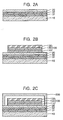
FIGS. 2A-2E illustrate cross-sectional views of sequential stages in a method of fabricating an OLED display device according to an embodiment of the present invention. - Embodiments of the present invention will now be described more fully hereinafter with reference to the accompanying drawings, in which exemplary embodiments of the invention are illustrated. Aspects of the invention may, however, be embodied in different forms and should not be construed as limited to the embodiments set forth herein. Rather, these embodiments are provided so that this disclosure will be thorough and complete, and will fully convey the scope of the invention to those skilled in the art.
- In the figures, the dimensions of layers, elements, and regions may be exaggerated for clarity of illustration. It will also be understood that when a layer or element is referred to as being "on" another layer, element, or substrate, it can be directly on the other layer, element, or substrate, or intervening layers and/or elements may also be present. Further, it will also be understood that when a layer or element is referred to as being "between" two layers or elements, it can be the only layer or element between the two layers or elements, or one or more intervening layers and/or elements may also be present. In addition, it will be understood that when an element is referred to as being "connected" or "coupled" to another element, it can be directly connected or coupled to the other element or intervening elements may be present. In contrast, when an element is referred to as being "directly connected" or "directly coupled" to another element, there are no intervening elements present. Like reference numerals refer to like elements throughout.
- As used herein, the expressions "at least one," "one or more," and "and/or" are open-ended expressions that are both conjunctive and disjunctive in operation. For example, each of the expressions "at least one of A, B, and C," "at least one of A, B, or C," "one or more of A, B, and C," "one or more of A, B, or C" and "A, B, and/or C" includes the following meanings: A alone; B alone; C alone; both A and B together; both A and C together; both B and C together; and all three of A, B, and C together. Further, these expressions are open-ended, unless expressly designated to the contrary by their combination with the term "consisting of." For example, the expression "at least one of A, B, and C" may also include an nth member, where n is greater than 3, whereas the expression "at least one selected from the group consisting of A, B, and C" does not.
-
FIGS. 1A-1C illustrate cross-sectional views of sequential stages in a method of joining a flexible layer to a support according to an embodiment of the present invention. For example, the flexible layer may function as a flexible substrate in a flexible flat panel display device, e.g., an OLED display device. - Referring to
FIG. 1A , asupport 10 and aflexible layer 20 may be provided. Thesupport 10 may have a predetermined strength to facilitate control of theflexible layer 20 during subsequent processes. Thesupport 10 may be formed of, e.g., one or more of metal, glass, silicon, and quartz. - The
flexible layer 20 may have excellent thermal stability, and may be formed of a material exhibiting characteristics of a diffusion barrier with respect to moisture and oxygen. For example, theflexible layer 20 may be formed of plastic, stainless steel (STS), thin metal film, and/or ultra-thin glass. Theflexible layer 20 may have a thickness of about 0.1 mm or less. - Referring to
FIG. 1B , afirst metal layer 31 may be formed on a surface of thesupport 10 to form a first stacked structure. Similarly, asecond metal layer 32 may be formed on a surface of theflexible layer 20 to form a second stacked structure. The first and second metal layers 31 and 32 may be formed by any suitable method. - Formation of the first and second metal layers 31 and 32 on the
support 10 andflexible layer 20, respectively, may substantially minimize surface roughness of thesupport 10 andflexible layer 20, so adhesion between thesupport 10 andflexible layer 20 in subsequent processes may be improved. In other words, the first and second metal layers 31 and 32 may prevent or substantially minimize non-uniform joining of thesupport 10 and theflexible layer 20 by minimizing surface roughness thereof. Also, the first and second metal layers 31 and 32 may be formed on respective surfaces of thesupport 10 and theflexible layer 20, i.e., surfaces facing one another, so grinding the respective surfaces of thesupport 10 and theflexible layer 20 may be substantially omitted during joining of thesupport 10 and theflexible layer 20 in subsequent processes. - Each of the first and second metal layers 31 and 32 may have a thickness of about 100 nm (1,000 angstroms) to about 1000 nm (10,000 angstroms), e.g., about 100 nm (1,000 angstroms). A metal layer having a thickness that is too low may have poor surface roughness, so joining of the
support 10 and theflexible layer 20 may be difficult. A metal layer having a thickness that is too thick, may damage theflexible layer 20 due to non-reversible force generated during detachment of thesupport 10 and theflexible layer 20. Therefore, a thickness of about 100 nm (1,000 angstroms) to about 1000 nm (10,000 angstroms) of the first and second metal layers 31 and 32 may provide uniform attachment between thesupport 10 and theflexible layer 20 in subsequent processes despite the surface roughness of thesupport 10 and theflexible layer 20. Thus, excessive production cost and time may be prevented. - Each of the first and second metal layers 31 and 32 may be formed of a material having a low melting point in order to facilitate a direct joining between the
support 10 and theflexible layer 20, e.g., via annealing, in a subsequent process. The first and second metal layers 31 and 32 may include one or more of iron (Fe), nickel (Ni), tin (Sn), zinc (Zn), chromium (Cr), cobalt (Co), magnesium (Mg), titanium (Ti), zirconium (Zr), aluminum (Al), silver (Ag), copper (Cu), and an alloy thereof. - Once the first and second metal layers 31 and 32 are formed on the
support 10 and on theflexible layer 20, respectively, by-products and/or foreign substances generated during formation of the first and second metal layers 31 and 32 may be removed by an initial cleaning process. The initial cleaning process may include one or more steps of cleaning, e.g., immersing the first and second metal layers 31 and 32 in any suitable cleaning fluid, followed by drying. For example, the initial cleaning process may include three cleaning steps. It is noted, however, that, e.g., a single-step initial cleaning process, two-step initial cleaning process, and so forth, are within the scope of the present invention. - In the first cleaning step of the initial cleaning process, by products and foreign substances may be removed from the first and second metal layers 31 and 32 using, e.g., a stripper. For example, each of the
support 10 with thefirst metal layer 31 and theflexible layer 20 with thesecond metal layer 32 may be immersed in a cleaning fluid, e.g., deionized (DI) water or an organic cleaning liquid, and may be subsequently dried using, e.g., isopropyl alcohol (IPA). - In the second cleaning step of the initial cleaning process, the first and second metal layers 31 and 32 may be cleaned by a D-sonic method or by a rinsing method. The D-sonic method may include immersing each of the
support 10 with thefirst metal layer 31 and theflexible layer 20 with thesecond metal layer 32 in DI water, while cleaning via high frequency sonic energy. The rinsing method may include rotating thesupport 10 with thefirst metal layer 31 and theflexible layer 20 with thesecond metal layer 32, while spraying thesupport 10 with thefirst metal layer 31 and theflexible layer 20 with thesecond metal layer 32 with DI water. - In the third cleaning step of the initial cleaning process, the first and second metal layers 31 and 32 may be cleaned using, e.g., a stripper. For example, each of the
support 10 with thefirst metal layer 31 and theflexible layer 20 with thesecond metal layer 32 may be immersed in a cleaning fluid, e.g., deionized (DI) water or an organic cleaning liquid, and may be subsequently dried using, e.g., isopropyl alcohol (IPA). The third cleaning step may be substantially the same as the first cleaning step. - Once the initial cleaning process of the first and second metal layers 31 and 32 is complete, each of the first and second metal layers 31 and 32 may be annealed at a temperature of about 100 °C to about 140 °C. The annealing process may completely remove the cleaning fluid used in the initial cleaning process to clean the first and second metal layers 31 and 32.
- Referring to
FIG. 1C , a joining process may be performed by joining the first and second stacked structures illustrated inFIG. 1B via the first and second metal layers 31 and 32. In other words, outer surfaces of the first and second metal layers 31 and 32 may be joined, such that thesupport 10 and theflexible layer 20 may be connected via the first and second metal layers 31 and 32 to form, e.g., a multi-layered structure, as illustrated inFIG. 1C . The joining process may include first and second joining steps. - In the first joining step, the
support 10 with thefirst metal layer 31 and theflexible layer 20 with thesecond metal layer 32 may be placed in aclass 100 clean room, such that thefirst metal layer 31 and thesecond metal layer 32 may be adjacent to each other. For example, the first and second metal layers 31 and 32 may be arranged in parallel and close proximity to each other. It is noted that theclass 100 clean room refers to a processing chamber maintaining a controlled environment in terms of airborn particles and temperature, so the temperature is maintained at about room temperature and the particles therein are in an amount of about one hundred particles in a 30 x 30 x 30 cm3 air space. Once the first and second metal layers 31 and 32 are arranged in the clean room, the first and second metal layers 31 and 32 may be joined by a chemical bond, e.g., a weak hydrogen bond, to form a stacked structure ofsupport 10/first metal layer 31/second metal layer 32/flexible layer 20, as illustrated inFIG. 1C . - Once the first and second metal layers 31 and 32 are joined by the first joining step, the first and second metal layers 31 and 32 may be cleaned by an intermediate cleaning process in two cleaning steps. In the first step of the intermediate cleaning process, the D-sonic or rinsing method described previously with reference to the second cleaning step of the initial cleaning process may be used. In the second step of the intermediate cleaning process, the joined
support 10 andflexible layer 20 may be dried after the first step of the intermediate cleaning process using, e.g., IPA. By the first and second steps of the intermediate cleaning processes, water and bubbles adsorbed between the surfaces of the first and second metal layers 31 and 32 may be removed. - Once the joined first and second metal layers 31 and 32 are cleaned and dried, the second joining step may be performed by pressing and annealing the first and second metal layers 31 and 32. While the first and second metal layers 31 and 32 are weakly joined by a hydrogen bond in the first joining step, the second joining process may increase the bonding strength between the first and second metal layers 31 and 32. In particular, as joining density between the first and second metal layers 31 and 32 is increased by applied heat and pressure, a distance between the first and second metal layers 31 and 32 may decrease and a metallic bond may be formed between the first and second metal layers 31 and 32 to directly join them together. Consequently, a distance between the
support 10 and theflexible layer 20 after the second joining step may be decreased at least about 5-fold, as compared to a distance between thesupport 10 and theflexible layer 20 after the first joining step and before the second joining step. For example, while a distance between the first and second metal layers 31 and 32 after the first joining step, i.e., due to the hydrogen bonding, may be about 2 nm (20 angstroms) to about 3 nm (30 angstroms), a distance between the first and second metal layers 31 and 32 after the second joining process, i.e., due to the metal bonding, may be about 0.3 nm (3 angstroms) to about 0.4 nm (4 angstroms). Therefore, joining strength may be also increased as compared to the joining strength immediately after the first joining step. - In the second joining step, the pressure applied to the
support 10 and theflexible layer 20 may be in a range of about 0.1 MPa to about 50 MPa. For example, the pressure may be about 0.5 MPa. A pressure above about 50 MPa may damage thesupport 10 and theflexible layer 20, and a pressure below about 0.1 MPa may be insufficient to provide high adhesion between thesupport 10 and theflexible layer 20. Further, in the second joining step, an annealing temperature for optimizing pressure and strength of the adhesion between thesupport 10 and theflexible layer 20 may be about 200 °C to about 600 °C, e.g., about 400 °C to about 450 °C. The annealing time may be about 0.5 hours to about 2 hours, e.g., about 0.5 hours. - According to another embodiment of the present invention, a method of joining a flexible layer with a support may be substantially similar to the method described previously with reference to
FIGS. 1A-1C , with the exception of performing hydrogen fluoride (HF) treatment on the first and second metal layers 31 and 32 after the initial cleaning process in order to make outer surfaces of the first and second metal layers 31 and 32 hydrophobic. Due to the HF treatment of the first and second metal layers 31 and 32, gases, e.g., oxygen, may be removed from the first and second metal layers 31 and 32, so the intermediate cleaning process for removing bubbles and water may be omitted. Thus, the HF-treated first and second metal layers 31 and 32 may be joined by a chemical bond through the first joining process, as described previously with reference toFIG. 1C , and may be directly joined by a metallic bond having a high adhesion in the second joining process, as further described with reference toFIG. 1C . - According to another embodiment illustrated in
FIGS. 2A-2E , a method of fabricating an OLED display device may include joining thesupport 10 and theflexible layer 20. A method of joining thesupport 10 and theflexible layer 20 may be either of the methods described previously, e.g., with reference toFIGS. 1A-1C . - Referring to
FIG. 2A , theflexible layer 20 may be formed on thesupport 10, such that the first and second metal layers 31 and 32 may be therebetween. The method of joining thesupport 10 to theflexible layer 20 may be substantially similar to the method described previously, e.g., with reference toFIGS. 1A-1C , and therefore will not be repeated. - Referring to
FIG. 2B , anOLED 100 may be formed on theflexible layer 20, such that theflexible layer 20 may be between theOLED 100 and thesupport 10. TheOLED 100 may include afirst electrode 110, anorganic layer 120, and asecond electrode 130 formed sequentially on theflexible layer 20, as further illustrated inFIG. 2B . A thin film transistor (not shown), a capacitor (not shown), or an insulating layer (not shown) may be further included between thefirst electrode 110 and theflexible layer 20. - The
first electrode 110 may have a double-structure or a triple-structure to include a reflective layer. For example, if thefirst electrode 110 has a double-structure, thefirst electrode 110 may include a sequentially stacked reflective layer, e.g., a layer including aluminum (Al), silver (Ag), or an alloy thereof, and a transparent conductive layer, e.g., a layer including indium-tin-oxide (ITO), indium-zinc-oxide (IZO), indium-tin-zinc-oxide (ITZO), or a combination thereof. In another example, if thefirst electrode 110 has a triple-structure, thefirst electrode 110 may include a sequentially stacked first metal layer, e.g., a layer including titanium (Ti), molybdenum (Mo), ITO, or an alloy thereof, a reflective layer, e.g., a layer including Al, Ag, or an alloy thereof, and a transparent conductive layer, e.g., a layer including ITO, IZO, ITZO, or a combination thereof. - The
organic layer 120 may include an organic light emitting layer. The organic light emitting layer may include one or more of a white emitting layer, a red emitting layer, a green emitting layer, and a blue emitting layer. Further, theorganic layer 120 may include at least one of a hole injection layer, a hole transport layer, an electron injection layer, an electron transport layer, and a hole blocking layer. Theorganic layer 120 may be formed by, e.g., vacuum deposition, ink-jet printing, or laser induced thermal imaging (LITI). - If the
organic layer 120 includes a white emitting layer, the white emitting layer may be a single layer or a multi-layer. When the white emitting layer is a single layer, white light may be emitted by mixing materials emitting different colors with different dopants. For example, white emitting layer having a single layer may include PBD, TPB, Coumarin 6, DCM1, and Nile red with a carbazole molecule, i.e., PVK, at an appropriate ratio. Alternatively, white light may be emitted by mixing two different color-emitting materials and adding the remaining emitting material thereto. For example, a white emitting layer having a single layer may include a red emitting material mixed with a green emitting material, followed by addition of a blue emitting material. The red emitting material may be formed of a polymer, e.g., polythiophene (PT) and derivatives thereof, the green emitting material may be formed of low-molecular materials, e.g., an aluminum quinoline complex (Alq3), BeBq2, and/or Almq, and/or a polymer, e.g., poly(p-phenylenevinylene) (PPV) and derivatives thereof, and the blue emitting material may be formed of low-molecular materials, e.g., ZnPBO, Balq, DPVBi and OXA-D, and/or polymers, e.g., polyphenylene (PPP) and derivatives thereof. - When the white emitting layer is a multi-layer, the white emitting layer may be formed to include, e.g., two layers emitting light in different wavelength regions. For example, one layer, e.g., a phosphorescent emitting layer, may emit light in an orange-red region and another layer, e.g., a fluorescent emitting layer, may emit light in a blue region. It is noted that the phosphorescent emitting layer may have excellent emission characteristics, as compared with a fluorescent emitting layer emitting light in a substantially same wavelength range, while the fluorescent emitting layer may have better lifetime characteristics than the phosphorescent emitting layer. Thus, the white emitting layer formed by stacking the phosphorescent emitting layer emitting light in the orange-red region and the fluorescent emitting layer emitting light in the blue region may have excellent luminous efficiency and long lifetime. Also, the white emitting layer may be a double layer formed of a polymer, a low-molecular material, and/or a combination thereof.
- When the white emitting layer is a multi-layer, the white emitting layer may have a triple structure. For example, the white emitting layer may include a red emitting layer, a green emitting layer, and a blue emitting layer. The red, green, and blue emitting layers may emit lights of respective colors, and may be stacked in any order. The red emitting layer may be formed of a low molecular material, e.g., Alq3 (host)/DCJTB (fluorescent dopant), Alq3 (host)/DCM (fluorescent dopant), or CBP (host)/PtOEP (phosphorescent organic metal complex), or of a polymer, e.g., a PFO series polymer. The green emitting layer may be formed of a low molecular material, e.g., Alq3, Alq3 (host)/C545t (dopant), or CBP (host)/IrPPY (phosphorescent organic material complex), or of a polymer, e.g., PFO series polymer or a PPV series polymer. The blue emitting layer may include a host and a dopant, wherein the host may include one or more of an amine series compound, e.g., TMM-004(COVION), 3-(4-tert-butylphenyl)-4-phenyl-5-(4-biphenylspiro)-6P, a PFO series polymer, and a PPV series polymer, and the dopant may include one or more of distyrylbenzene (DSB), distyrylarylene (DSA), bis[2-(4,6-difluorophenyl)pyridinato-N,C2']iridium picolinate (F2Irpic), and tris[1-(4,6-difluorophenyl)pyrazolate-N,C2']iridium (Ir[dfppz]3).
- The hole injection layer of the
organic layer 120 may facilitate hole injection into the organic emitting layer of theorganic layer 120, and may increase the lifetime of theOLED 100. The hole injection layer may be formed of an arylamine series compound or starburst amines, and examples of hole injection layer materials may include one or more of 4,4,4-tris(3-methylphenylamino) triphenylamine (m-MTDATA), 1,3,5-tris[4-(3-methylphenylamino)phenyl]benzene (m-MTDATB), and copper phthalocyanine (CuPc). - The hole transport layer of the
organic layer 120 may be formed of an arylene diamine derivative, a starburst compound, a biphenyl diamine derivative having a spiro group, or a trapezoidal compound. Examples of materials used to form the hole transport layer may include one or more of N,N-diphenyl-N,N-bis(4-methylphenyl)-1,1-biphenyl-4,4-diamine (TPD) or 4,4-bis[N-(1-naphthyl)-N-phenylamino]biphenyl (NPB). - The hole blocking layer of the
organic layer 120 may prevent transfer of a hole into the electron injection layer when hole mobility is greater than electron mobility in the organic emitting layer. The hole blocking layer may be formed of, e.g., 2-biphenyl-4-yl-5-(4-biphenyl)-1,2,4-triazole (TAZ). - The electron transport layer may be formed of a metal compound that may receive an electron from a cathode electrode and stably transfer the electron, e.g., e.g., Alq3. The electron injection layer may be formed of, e.g., one or more of 1,3,4-oxyldiazole derivatives, 1,2,4-triazole derivatives, and LiF.
- The
second electrode 130 of theOLED 100 may be a semi-transmissive electrode, and may be formed of, e.g., magnesium silver (MgAg) or aluminum silver (AlAg). For example, MgAg may be formed by co-deposition of Mg and Ag, and AlAg may be formed by sequentially depositing Al and Ag. Further, a transparent conductive layer, e.g., ITO or IZO, may be further formed on thesecond electrode 130. - Referring to
FIG. 2C , anencapsulation substrate 200 may be formed on theflexible layer 20 to surround theOLED 100, such that theOLED 100 may be completely enclosed from an exterior. In other words, theencapsulation substrate 200 may protect theOLED 100 from moisture and/or external air. Theencapsulation substrate 200 may be formed of transparent glass or plastic to transmit light emitted from theOLED 100. Theencapsulation substrate 200 and theflexible layer 20 may be adhered by a sealant or a frit. - Referring to
FIG. 2D , once theOLED 100 is enclosed between theflexible layer 20 and theencapsulation substrate 200, theflexible layer 20 may be detached from thesupport 10 usingdetachment equipment 300, e.g., a razor blade. As illustrated inFIG. 2D , thedetachment equipment 300 may be used along an interface between theflexible layer 20 and thesecond metal layer 32, so thesupport 10 and the first and second metal layers 131 and 132 may be completely removed. - Accordingly, as illustrated in
FIG. 2E , thesupport 10 and theflexible layer 20 are separated from each other. Thus, an OLED display device according to an exemplary embodiment of the present invention may include a flexible substrate, i.e., theflexible layer 20. - Embodiments of the present invention may be advantageous in providing a method of joining a flexible layer to a support by using metal layers therebetween. Use of the metal layers may eliminate use of an organic adhesive, so organic contamination may be eliminated and temperature dependency may be reduced. Further, use of the metal layers may minimize surface roughness of the flexible layer and the support, so uniformity adhesion and strength between the flexible layer and the support may be increased. As such, manufacturing time and costs may be reduced, while manufacturing yield may be increased. Further the manufacturing process may be simplified. Accordingly, manufacturing of an OLED display device with a flexible substrate according to embodiments of the present invention may be substantially improved in terms of manufacturing process and costs.
- Exemplary embodiments of the present invention have been disclosed herein, and although specific terms are employed, they are used and are to be interpreted in a generic and descriptive sense only and not for purpose of limitation. Accordingly, it will be understood by those of ordinary skill in the art that various changes in form and details may be made without departing from the scope of the present invention as set forth in the following claims.
Claims (11)
- A method of joining a flexible layer and a support, comprising:forming a first metal layer on one surface of the support;forming a second metal layer on one surface of the flexible layer;cleaning the first metal layer and the second metal layer; andjoining the second metal layer to the first metal layer, such that the second metal layer is between the flexible layer and the first metal layer.
- A method according to claim 1, wherein cleaning the first and second metal layers includes:a first cleaning step, the first cleaning step including drying the first and second metal layers after immersion thereof in a cleaning fluid;a second cleaning step, the second cleaning step including cleaning the first and second metal layers via a D-sonic process or a rinsing process in deionized water; anda third cleaning step, the third cleaning step being substantially same as the first cleaning step.
- A method according to claim 1 or 2, wherein the first and second metal layers are formed of one or more of iron, nickel, tin, zinc, chromium, cobalt, silicon, magnesium, titanium, zirconium, aluminum, silver, copper, and an alloy thereof.
- A method according to any one of claims 1 to 3, wherein joining the first and second metal layers includes:a first joining process, the first joining process including positioning the first and second metal layers adjacent to each other at room temperature;an intermediate cleaning process, the intermediate cleaning process including cleaning the first and second metal layers via a D-sonic process or a rinsing process in deionized water, and drying the first and second metal layers using isopropyl alcohol; anda second joining process, the second joining process including pressing and annealing the first and second metal layers to each other.
- A method according to claim 1, further comprising treating the first and second metal layers with hydrogen fluoride after the cleaning and before the joining.
- A method according to claim 1, further comprising treating the first and second metal layers with hydrogen fluoride after the cleaning.
- A method according to claim 5 or 6, wherein cleaning the first and second metal layers includes:a first cleaning step, the first cleaning step including drying the first and second metal layers after immersion thereof in a cleaning fluid;a second cleaning step, the second cleaning step including cleaning the first and second metal layers via a D-sonic process or a rinsing process in deionized water; anda third cleaning step, the third cleaning step being substantially same as the first cleaning step.
- A method according to any one of claims 5 to 7, wherein the first and second metal layers are formed of one or more of iron, nickel, tin, zinc, chromium, cobalt, silicon, magnesium, titanium, zirconium, aluminum, silver, copper, and an alloy thereof.
- A method according to any one of claims 5 to 8, wherein joining the first and second metal layers includes:a first joining process, the first joining process including positioning the first and second metal layers adjacent to each other at room temperature; anda second joining process, the second joining process including pressing and annealing the first and second metal layers to each other.
- A method according to any one of claims 1 to 9, wherein each of the first and second metal layers is formed to a thickness of about 100 nm to about 1,000 nm.
- A method of fabricating an organic light emitting diode (OLED) display device, comprising:joining a flexible layer and a support according to a method of any one of claims 1 to 10;forming an OLED on the flexible layer, such that the flexible layer is between the OLED and the support, the OLED including a first electrode, an organic layer having a light emitting layer, and a second electrode; andremoving the support with the first and second metal layers.
Applications Claiming Priority (1)
| Application Number | Priority Date | Filing Date | Title |
|---|---|---|---|
| KR1020070072199A KR100889625B1 (en) | 2007-07-19 | 2007-07-19 | Bonding method and manufacturing method of organic light emitting display device using the same |
Publications (3)
| Publication Number | Publication Date |
|---|---|
| EP2022626A2 true EP2022626A2 (en) | 2009-02-11 |
| EP2022626A3 EP2022626A3 (en) | 2009-05-27 |
| EP2022626B1 EP2022626B1 (en) | 2011-10-26 |
Family
ID=40202089
Family Applications (1)
| Application Number | Title | Priority Date | Filing Date |
|---|---|---|---|
| EP08252458A Ceased EP2022626B1 (en) | 2007-07-19 | 2008-07-18 | Method of joining and method of fabricating an organic light emitting diode display device using the same |
Country Status (6)
| Country | Link |
|---|---|
| US (2) | US8016628B2 (en) |
| EP (1) | EP2022626B1 (en) |
| JP (1) | JP4750779B2 (en) |
| KR (1) | KR100889625B1 (en) |
| CN (1) | CN101351063B (en) |
| TW (1) | TWI356001B (en) |
Cited By (1)
| Publication number | Priority date | Publication date | Assignee | Title |
|---|---|---|---|---|
| EP2551895A1 (en) * | 2011-07-27 | 2013-01-30 | STMicroelectronics S.r.l. | Method of manufacturing an electronic device having a plastic substrate |
Families Citing this family (17)
| Publication number | Priority date | Publication date | Assignee | Title |
|---|---|---|---|---|
| JP2010192701A (en) * | 2009-02-18 | 2010-09-02 | Showa Denko Kk | Light emitting diode, light emitting diode lamp, and method of manufacturing the light emitting diode |
| US8246867B2 (en) * | 2009-10-16 | 2012-08-21 | Corning Incorporated | Method for assembling an optoelectronic device |
| KR101084230B1 (en) * | 2009-11-16 | 2011-11-16 | 삼성모바일디스플레이주식회사 | Organic light emitting display device and manufacturing method of organic light emitting display device |
| US9184094B1 (en) * | 2012-01-26 | 2015-11-10 | Skorpios Technologies, Inc. | Method and system for forming a membrane over a cavity |
| US8916954B2 (en) * | 2012-02-05 | 2014-12-23 | Gtat Corporation | Multi-layer metal support |
| US8841161B2 (en) | 2012-02-05 | 2014-09-23 | GTAT.Corporation | Method for forming flexible solar cells |
| US8785294B2 (en) | 2012-07-26 | 2014-07-22 | Gtat Corporation | Silicon carbide lamina |
| CN103682177B (en) * | 2013-12-16 | 2015-03-25 | 深圳市华星光电技术有限公司 | Manufacturing method of flexible OLED panel |
| US20160181574A1 (en) * | 2014-01-03 | 2016-06-23 | Shenzhen China Star Optoelectronics Technology Co., Ltd. | Method for manufacturing flexible oled (organic light emitting diode) panel |
| US9425221B2 (en) | 2014-01-31 | 2016-08-23 | Sharp Laboratories Of America, Inc. | Circuit-on-wire |
| US9299725B2 (en) | 2014-01-31 | 2016-03-29 | Sharp Laboratories Of America, Inc. | Fabrication process using circuit-on-wire |
| KR102459818B1 (en) | 2015-05-06 | 2022-10-27 | 삼성디스플레이 주식회사 | Organic light emitting diode display |
| KR102407115B1 (en) | 2015-06-25 | 2022-06-09 | 삼성디스플레이 주식회사 | Organic light emitting diode display |
| CN105493287B (en) * | 2015-09-18 | 2018-11-30 | 京东方科技集团股份有限公司 | A kind of preparation method of flexible display apparatus |
| US11495548B2 (en) * | 2017-12-20 | 2022-11-08 | Alpha And Omega Semiconductor International Lp | Semiconductor package having thin substrate and method of making the same |
| KR102712662B1 (en) * | 2019-05-27 | 2024-10-04 | 삼성디스플레이 주식회사 | Display apparatus and manufacturing method for the same |
| US11776820B2 (en) * | 2020-09-30 | 2023-10-03 | Huawei Technologies Co., Ltd. | Vertical interconnection structure and manufacturing method thereof, packaged chip, and chip packaging method |
Family Cites Families (51)
| Publication number | Priority date | Publication date | Assignee | Title |
|---|---|---|---|---|
| US2559864A (en) | 1948-03-24 | 1951-07-10 | Firth Francis George | Production of high frequency waves in a liquid medium |
| US2961354A (en) | 1958-10-28 | 1960-11-22 | Bell Telephone Labor Inc | Surface treatment of semiconductive devices |
| US5418002A (en) | 1990-12-24 | 1995-05-23 | Harris Corporation | Direct bonding of copper to aluminum nitride substrates |
| DE4115046A1 (en) | 1991-05-08 | 1992-11-12 | Fraunhofer Ges Forschung | DIRECT SUBSTRATE BONDING |
| US5876859A (en) | 1994-11-10 | 1999-03-02 | Vlt Corporation | Direct metal bonding |
| US5996594A (en) * | 1994-11-30 | 1999-12-07 | Texas Instruments Incorporated | Post-chemical mechanical planarization clean-up process using post-polish scrubbing |
| US5915193A (en) | 1995-05-18 | 1999-06-22 | Tong; Qin-Yi | Method for the cleaning and direct bonding of solids |
| JP3892102B2 (en) | 1997-04-14 | 2007-03-14 | 大日本スクリーン製造株式会社 | Substrate processing method and apparatus |
| KR100328797B1 (en) | 1997-04-14 | 2002-09-27 | 다이닛뽕스크린 세이조오 가부시키가이샤 | Substrate Drying Equipment and Substrate Processing Equipment |
| AU9296098A (en) | 1997-08-29 | 1999-03-16 | Sharon N. Farrens | In situ plasma wafer bonding method |
| JPH11165951A (en) | 1997-10-01 | 1999-06-22 | Ogura Clutch Co Ltd | Tension device |
| US6131795A (en) | 1997-11-10 | 2000-10-17 | Matsushita Electric Industrial Co., Ltd. | Thermal compression bonding method of electronic part with solder bump |
| JP2000311781A (en) | 1999-04-28 | 2000-11-07 | Hokuriku Electric Ind Co Ltd | Organic el element, and manufacture thereof |
| JP2000353797A (en) | 1999-06-11 | 2000-12-19 | Mitsubishi Electric Corp | Semiconductor wafer and method of manufacturing the same |
| KR100386954B1 (en) | 2000-11-17 | 2003-06-09 | 주영창 | Low Temperature Direct Bonding Method of Glass Substrate and Silicon Wafer |
| JP2002192651A (en) | 2000-12-25 | 2002-07-10 | Matsushita Electric Works Ltd | Moldings with metal coating and manufacturing method therefor |
| JP3734758B2 (en) | 2001-02-21 | 2006-01-11 | パナック株式会社 | Metal layer transfer film and metal layer transfer method |
| FR2823599B1 (en) * | 2001-04-13 | 2004-12-17 | Commissariat Energie Atomique | DEMOMTABLE SUBSTRATE WITH CONTROLLED MECHANICAL HOLDING AND METHOD OF MAKING |
| US20030188553A1 (en) | 2002-04-08 | 2003-10-09 | Mann Larry G. | Direct bonding methods using lithium |
| JP2004006707A (en) | 2002-04-26 | 2004-01-08 | Toray Eng Co Ltd | Mounting method and mounting device |
| US6642092B1 (en) | 2002-07-11 | 2003-11-04 | Sharp Laboratories Of America, Inc. | Thin-film transistors formed on a metal foil substrate |
| JP2004119430A (en) | 2002-09-24 | 2004-04-15 | Tadatomo Suga | Joining apparatus and method |
| JP2004144970A (en) | 2002-10-24 | 2004-05-20 | Toppan Printing Co Ltd | Laminated film for display |
| US6787885B2 (en) | 2002-11-04 | 2004-09-07 | The United States Of America As Represented By The Secretary Of The Navy | Low temperature hydrophobic direct wafer bonding |
| EP1568077B1 (en) | 2002-12-04 | 2018-07-11 | Suss MicroTec Lithography GmbH | Method for pre-treating surfaces of substrates to be bonded |
| JP2004191463A (en) | 2002-12-09 | 2004-07-08 | Hitachi Metals Ltd | Substrate for display and method for manufacturing the same |
| US8222072B2 (en) * | 2002-12-20 | 2012-07-17 | The Trustees Of Princeton University | Methods of fabricating devices by low pressure cold welding |
| WO2004073971A1 (en) | 2003-02-20 | 2004-09-02 | N.V. Bekaert S.A. | A method of manufacturing a laminated structure |
| US20050001201A1 (en) | 2003-07-03 | 2005-01-06 | Bocko Peter L. | Glass product for use in ultra-thin glass display applications |
| US20060207967A1 (en) | 2003-07-03 | 2006-09-21 | Bocko Peter L | Porous processing carrier for flexible substrates |
| US6949403B2 (en) | 2003-07-22 | 2005-09-27 | Organic Vision Inc. | Non-vacuum methods for the fabrication of organic semiconductor devices |
| JP2005064243A (en) | 2003-08-12 | 2005-03-10 | Dowa Mining Co Ltd | Method and apparatus for manufacturing metal-coated substrate |
| JP3980539B2 (en) | 2003-08-29 | 2007-09-26 | 唯知 須賀 | Substrate bonding method, irradiation method, and substrate bonding apparatus |
| JP4256763B2 (en) | 2003-11-19 | 2009-04-22 | 東京エレクトロン株式会社 | Plasma processing method and plasma processing apparatus |
| JP4397702B2 (en) | 2004-02-04 | 2010-01-13 | 三菱伸銅株式会社 | Method for producing metallized polyimide film |
| WO2005076756A2 (en) | 2004-02-12 | 2005-08-25 | Samsung Electronics Co., Ltd. | Flat panel display apparatus |
| KR101007722B1 (en) | 2004-02-12 | 2011-01-13 | 삼성전자주식회사 | Flat Panel Display and Manufacturing Method |
| JP2005256061A (en) | 2004-03-10 | 2005-09-22 | Dainippon Printing Co Ltd | Laminated body |
| US7087134B2 (en) | 2004-03-31 | 2006-08-08 | Hewlett-Packard Development Company, L.P. | System and method for direct-bonding of substrates |
| KR100615217B1 (en) | 2004-04-29 | 2006-08-25 | 삼성에스디아이 주식회사 | Manufacturing Method of Flat Panel Display |
| JP4494873B2 (en) | 2004-06-02 | 2010-06-30 | 株式会社アルバック | Printed wiring board, printed wiring board manufacturing method and manufacturing apparatus therefor |
| KR101100880B1 (en) * | 2004-09-24 | 2012-01-02 | 삼성전자주식회사 | Manufacturing Method of Flexible Display |
| JP4548828B2 (en) | 2004-10-29 | 2010-09-22 | Dowaホールディングス株式会社 | Method for manufacturing metal-coated substrate |
| EP1670298A1 (en) | 2004-12-07 | 2006-06-14 | Samsung SDI Germany GmbH | Substrate for a display and method for manufacturing the same |
| US20060135028A1 (en) | 2004-12-07 | 2006-06-22 | Andreas Klyszcz | Substrate for a display and method for manufacturing the same |
| KR100571848B1 (en) | 2005-01-05 | 2006-04-17 | 삼성전자주식회사 | Silicon direct bonding method |
| JP4624812B2 (en) * | 2005-01-20 | 2011-02-02 | 信越化学工業株式会社 | Manufacturing method of SOI wafer |
| JP4699822B2 (en) * | 2005-07-04 | 2011-06-15 | 株式会社豊田中央研究所 | Manufacturing method of semiconductor module |
| CN1711000A (en) | 2005-07-19 | 2005-12-21 | 天津理工大学 | Flexible white organic electroluminescent device and its preparation method |
| FR2893750B1 (en) * | 2005-11-22 | 2008-03-14 | Commissariat Energie Atomique | METHOD FOR MANUFACTURING SCREEN TYPE FLEXIBLE ELECTRONIC DEVICE COMPRISING A PLURALITY OF THIN FILM COMPONENTS |
| KR100841376B1 (en) * | 2007-06-12 | 2008-06-26 | 삼성에스디아이 주식회사 | Bonding method and manufacturing method of organic light emitting display device using the same |
-
2007
- 2007-07-19 KR KR1020070072199A patent/KR100889625B1/en not_active Expired - Fee Related
- 2007-12-13 JP JP2007322222A patent/JP4750779B2/en not_active Expired - Fee Related
-
2008
- 2008-07-04 TW TW097125453A patent/TWI356001B/en not_active IP Right Cessation
- 2008-07-18 CN CN2008101320158A patent/CN101351063B/en active Active
- 2008-07-18 EP EP08252458A patent/EP2022626B1/en not_active Ceased
- 2008-07-21 US US12/219,380 patent/US8016628B2/en active Active
-
2011
- 2011-09-07 US US13/227,091 patent/US8187960B2/en active Active
Cited By (1)
| Publication number | Priority date | Publication date | Assignee | Title |
|---|---|---|---|---|
| EP2551895A1 (en) * | 2011-07-27 | 2013-01-30 | STMicroelectronics S.r.l. | Method of manufacturing an electronic device having a plastic substrate |
Also Published As
| Publication number | Publication date |
|---|---|
| TWI356001B (en) | 2012-01-11 |
| JP2009026731A (en) | 2009-02-05 |
| TW200906623A (en) | 2009-02-16 |
| US20110315314A1 (en) | 2011-12-29 |
| US20090020592A1 (en) | 2009-01-22 |
| CN101351063B (en) | 2011-04-13 |
| EP2022626A3 (en) | 2009-05-27 |
| KR100889625B1 (en) | 2009-03-20 |
| US8016628B2 (en) | 2011-09-13 |
| CN101351063A (en) | 2009-01-21 |
| KR20090008877A (en) | 2009-01-22 |
| JP4750779B2 (en) | 2011-08-17 |
| EP2022626B1 (en) | 2011-10-26 |
| US8187960B2 (en) | 2012-05-29 |
Similar Documents
| Publication | Publication Date | Title |
|---|---|---|
| EP2022626B1 (en) | Method of joining and method of fabricating an organic light emitting diode display device using the same | |
| US7950567B2 (en) | Organic light emitting diode display device and method of fabricating the same | |
| US7994713B2 (en) | Organic light emitting diode and method of fabricating the same | |
| JP2006156390A (en) | Organic electroluminescent device and manufacturing method thereof | |
| US8486857B2 (en) | Donor substrate for laser induced thermal imaging and method of fabricating organic light emitting diode using the same | |
| JP2012001762A (en) | Vapor deposition method and vapor deposition device | |
| JP5960397B2 (en) | Organic light emitting device | |
| JP2008269964A (en) | Method for manufacturing electroluminescent element | |
| JP2013251191A (en) | Organic electroluminescent element | |
| KR101482313B1 (en) | Encapsulant for Packaging an Organic Electric Device, Method for Preparing the Same, Method for Encapsulating the Organic Electric Device by Using the Same and Organic Electric Device Packaged by the same | |
| JP2005212229A (en) | Transparent gas barrier film and electroluminescence device | |
| EP1744382B1 (en) | Organic light emitting display device | |
| US8227092B2 (en) | Organic electroluminescent device | |
| JP2016091793A (en) | Organic electroluminescence device and manufacturing method thereof | |
| EP2830396A1 (en) | Organic el device manufacturing method and organic el device | |
| KR100841375B1 (en) | Bonding method and manufacturing method of organic light emitting display device using the same | |
| US20060182878A1 (en) | Method of producing electronic device | |
| JP2009021126A (en) | Transfer material, pattern film forming method, and light emitting device manufacturing method | |
| US9412947B2 (en) | OLED fabrication using laser transfer | |
| KR101616714B1 (en) | Method for Releasing thin film and Method for Manufacturing Organic Electronic Device | |
| KR100712296B1 (en) | Organic electroluminescent device having a plurality of light emitting units | |
| JP2010033984A (en) | Organic light-emitting device | |
| JP2002367777A (en) | Method for manufacturing organic electroluminescence device | |
| KR100770271B1 (en) | Donor substrate for laser transfer, manufacturing method thereof and manufacturing method of organic light emitting device using same | |
| JP2004079317A (en) | Manufacturing method for organic electroluminescent element and organic electroluminescent element |
Legal Events
| Date | Code | Title | Description |
|---|---|---|---|
| PUAI | Public reference made under article 153(3) epc to a published international application that has entered the european phase |
Free format text: ORIGINAL CODE: 0009012 |
|
| 17P | Request for examination filed |
Effective date: 20080724 |
|
| AK | Designated contracting states |
Kind code of ref document: A2 Designated state(s): AT BE BG CH CY CZ DE DK EE ES FI FR GB GR HR HU IE IS IT LI LT LU LV MC MT NL NO PL PT RO SE SI SK TR |
|
| AX | Request for extension of the european patent |
Extension state: AL BA MK RS |
|
| RAP1 | Party data changed (applicant data changed or rights of an application transferred) |
Owner name: SAMSUNG MOBILE DISPLAY CO., LTD. |
|
| RIN1 | Information on inventor provided before grant (corrected) |
Inventor name: KIM, HYO-JIN C/O SAMSUNG MOBILE DISPLAY CO. LTD. Inventor name: KWACK, JIN-HO Inventor name: JEONG, JAE-KYEONG C/O SAMSUNG MOBILE DISPLAY CO. Inventor name: LEE, KYU-SUNG C/O SAMSUNG MOBILE DISPLAY CO. LTD. Inventor name: LEE, JAE-SEOB |
|
| PUAL | Search report despatched |
Free format text: ORIGINAL CODE: 0009013 |
|
| AK | Designated contracting states |
Kind code of ref document: A3 Designated state(s): AT BE BG CH CY CZ DE DK EE ES FI FR GB GR HR HU IE IS IT LI LT LU LV MC MT NL NO PL PT RO SE SI SK TR |
|
| AX | Request for extension of the european patent |
Extension state: AL BA MK RS |
|
| RIC1 | Information provided on ipc code assigned before grant |
Ipc: B32B 15/08 20060101ALI20090417BHEP Ipc: B32B 15/00 20060101AFI20090108BHEP Ipc: H01L 51/00 20060101ALI20090417BHEP |
|
| AKX | Designation fees paid |
Designated state(s): DE FR GB HU |
|
| GRAP | Despatch of communication of intention to grant a patent |
Free format text: ORIGINAL CODE: EPIDOSNIGR1 |
|
| GRAS | Grant fee paid |
Free format text: ORIGINAL CODE: EPIDOSNIGR3 |
|
| GRAA | (expected) grant |
Free format text: ORIGINAL CODE: 0009210 |
|
| AK | Designated contracting states |
Kind code of ref document: B1 Designated state(s): DE FR GB HU |
|
| REG | Reference to a national code |
Ref country code: GB Ref legal event code: FG4D |
|
| REG | Reference to a national code |
Ref country code: DE Ref legal event code: R096 Ref document number: 602008010802 Country of ref document: DE Effective date: 20120105 |
|
| PLBE | No opposition filed within time limit |
Free format text: ORIGINAL CODE: 0009261 |
|
| STAA | Information on the status of an ep patent application or granted ep patent |
Free format text: STATUS: NO OPPOSITION FILED WITHIN TIME LIMIT |
|
| 26N | No opposition filed |
Effective date: 20120727 |
|
| REG | Reference to a national code |
Ref country code: DE Ref legal event code: R097 Ref document number: 602008010802 Country of ref document: DE Effective date: 20120727 |
|
| REG | Reference to a national code |
Ref country code: FR Ref legal event code: TP Owner name: SAMSUNG DISPLAY CO., LTD., KR Effective date: 20121226 |
|
| REG | Reference to a national code |
Ref country code: GB Ref legal event code: 732E Free format text: REGISTERED BETWEEN 20130103 AND 20130109 |
|
| REG | Reference to a national code |
Ref country code: DE Ref legal event code: R082 Ref document number: 602008010802 Country of ref document: DE Representative=s name: GULDE HENGELHAUPT ZIEBIG & SCHNEIDER, DE |
|
| REG | Reference to a national code |
Ref country code: DE Ref legal event code: R081 Ref document number: 602008010802 Country of ref document: DE Owner name: SAMSUNG DISPLAY CO., LTD., KR Free format text: FORMER OWNER: SAMSUNG MOBILE DISPLAY CO. LTD., SUWON, KR Effective date: 20130201 Ref country code: DE Ref legal event code: R082 Ref document number: 602008010802 Country of ref document: DE Representative=s name: GULDE HENGELHAUPT ZIEBIG & SCHNEIDER, DE Effective date: 20130201 Ref country code: DE Ref legal event code: R081 Ref document number: 602008010802 Country of ref document: DE Owner name: SAMSUNG DISPLAY CO., LTD., YONGIN-CITY, KR Free format text: FORMER OWNER: SAMSUNG MOBILE DISPLAY CO. LTD., SUWON, GYEONGGI, KR Effective date: 20130201 Ref country code: DE Ref legal event code: R082 Ref document number: 602008010802 Country of ref document: DE Representative=s name: GULDE & PARTNER PATENT- UND RECHTSANWALTSKANZL, DE Effective date: 20130201 |
|
| PG25 | Lapsed in a contracting state [announced via postgrant information from national office to epo] |
Ref country code: HU Free format text: LAPSE BECAUSE OF FAILURE TO SUBMIT A TRANSLATION OF THE DESCRIPTION OR TO PAY THE FEE WITHIN THE PRESCRIBED TIME-LIMIT Effective date: 20080718 |
|
| REG | Reference to a national code |
Ref country code: FR Ref legal event code: PLFP Year of fee payment: 9 |
|
| REG | Reference to a national code |
Ref country code: FR Ref legal event code: PLFP Year of fee payment: 10 |
|
| REG | Reference to a national code |
Ref country code: FR Ref legal event code: PLFP Year of fee payment: 11 |
|
| P01 | Opt-out of the competence of the unified patent court (upc) registered |
Effective date: 20230515 |
|
| PGFP | Annual fee paid to national office [announced via postgrant information from national office to epo] |
Ref country code: GB Payment date: 20240620 Year of fee payment: 17 |
|
| PGFP | Annual fee paid to national office [announced via postgrant information from national office to epo] |
Ref country code: FR Payment date: 20240624 Year of fee payment: 17 |
|
| PGFP | Annual fee paid to national office [announced via postgrant information from national office to epo] |
Ref country code: DE Payment date: 20240620 Year of fee payment: 17 |
|
| REG | Reference to a national code |
Ref country code: DE Ref legal event code: R119 Ref document number: 602008010802 Country of ref document: DE |
|
| GBPC | Gb: european patent ceased through non-payment of renewal fee |
Effective date: 20250718 |
|
| PG25 | Lapsed in a contracting state [announced via postgrant information from national office to epo] |
Ref country code: GB Free format text: LAPSE BECAUSE OF NON-PAYMENT OF DUE FEES Effective date: 20250718 |
|
| PG25 | Lapsed in a contracting state [announced via postgrant information from national office to epo] |
Ref country code: DE Free format text: LAPSE BECAUSE OF NON-PAYMENT OF DUE FEES Effective date: 20260203 |
|
| PG25 | Lapsed in a contracting state [announced via postgrant information from national office to epo] |
Ref country code: FR Free format text: LAPSE BECAUSE OF NON-PAYMENT OF DUE FEES Effective date: 20250731 |