US8227092B2 - Organic electroluminescent device - Google Patents
Organic electroluminescent device Download PDFInfo
- Publication number
- US8227092B2 US8227092B2 US11/633,005 US63300506A US8227092B2 US 8227092 B2 US8227092 B2 US 8227092B2 US 63300506 A US63300506 A US 63300506A US 8227092 B2 US8227092 B2 US 8227092B2
- Authority
- US
- United States
- Prior art keywords
- layer
- titanium oxide
- alkyl group
- electroluminescent device
- organic electroluminescent
- Prior art date
- Legal status (The legal status is an assumption and is not a legal conclusion. Google has not performed a legal analysis and makes no representation as to the accuracy of the status listed.)
- Active, expires
Links
- 0 *[Ti+]1(*)(*)O/C([5*])=[O-]\[Ti+](C)(C)(C)O/C([5*])=[O-]\1 Chemical compound *[Ti+]1(*)(*)O/C([5*])=[O-]\[Ti+](C)(C)(C)O/C([5*])=[O-]\1 0.000 description 14
- DSNLMLQHLQGWTM-UHFFFAOYSA-N C.CC(=O)C1=CC2=C(C=C(N(C3=CC=CC=C3)C3=CC=CC=C3)C=C2)OC1=O Chemical compound C.CC(=O)C1=CC2=C(C=C(N(C3=CC=CC=C3)C3=CC=CC=C3)C=C2)OC1=O DSNLMLQHLQGWTM-UHFFFAOYSA-N 0.000 description 2
- DIVZFUBWFAOMCW-UHFFFAOYSA-N CC1=CC=CC(N(C2=CC=CC=C2)C2=CC=C(N(C3=CC=C(N(C4=CC=CC=C4)C4=CC=CC(C)=C4)C=C3)C3=CC=C(N(C4=CC=CC=C4)C4=CC(C)=CC=C4)C=C3)C=C2)=C1 Chemical compound CC1=CC=CC(N(C2=CC=CC=C2)C2=CC=C(N(C3=CC=C(N(C4=CC=CC=C4)C4=CC=CC(C)=C4)C=C3)C3=CC=C(N(C4=CC=CC=C4)C4=CC(C)=CC=C4)C=C3)C=C2)=C1 DIVZFUBWFAOMCW-UHFFFAOYSA-N 0.000 description 2
- VGECVTNMDIJVMZ-UHFFFAOYSA-N C#CC#CC#CC.CCN(C)C1=CC2=C(C=C1)C=C(C1=NC3=C(C=CC=C3)N1)C(=O)O2 Chemical compound C#CC#CC#CC.CCN(C)C1=CC2=C(C=C1)C=C(C1=NC3=C(C=CC=C3)N1)C(=O)O2 VGECVTNMDIJVMZ-UHFFFAOYSA-N 0.000 description 1
- QGEGGACALYTCIM-UHFFFAOYSA-N C#CC#CC#CS.O=C1OC2=C(C=CC(N(C3=CC=CC=C3)C3=CC=CC=C3)=C2)C=C1C1=NC2=C(C=CC=C2)S1 Chemical compound C#CC#CC#CS.O=C1OC2=C(C=CC(N(C3=CC=CC=C3)C3=CC=CC=C3)=C2)C=C1C1=NC2=C(C=CC=C2)S1 QGEGGACALYTCIM-UHFFFAOYSA-N 0.000 description 1
- DCUQOTQPOJTEJP-PPQSCVLNSA-N C.C1=CC=C(N(C2=CC=C(C3=CC=C(N(C4=CC=CC=C4)C4=C5C=CC=CC5=CC=C4)C=C3)C=C2)C2=CC=CC3=C2C=CC=C3)C=C1.CC1=CC=CC(N(C2=CC=CC=C2)C2=CC=C(C3=CC=C(N(C4=CC=CC=C4)C4=CC=CC(C)=C4)C=C3)C=C2)=C1.[2H]P[3H] Chemical compound C.C1=CC=C(N(C2=CC=C(C3=CC=C(N(C4=CC=CC=C4)C4=C5C=CC=CC5=CC=C4)C=C3)C=C2)C2=CC=CC3=C2C=CC=C3)C=C1.CC1=CC=CC(N(C2=CC=CC=C2)C2=CC=C(C3=CC=C(N(C4=CC=CC=C4)C4=CC=CC(C)=C4)C=C3)C=C2)=C1.[2H]P[3H] DCUQOTQPOJTEJP-PPQSCVLNSA-N 0.000 description 1
- ZKJNPUUFZWRZKV-UHFFFAOYSA-N C.CC(=O)C1=CC2=C(OC1=O)C1=C3C(=C2)C(C)(C)CCN3CCC1(C)C Chemical compound C.CC(=O)C1=CC2=C(OC1=O)C1=C3C(=C2)C(C)(C)CCN3CCC1(C)C ZKJNPUUFZWRZKV-UHFFFAOYSA-N 0.000 description 1
- OSVIEEDVHXCNDZ-UHFFFAOYSA-N C.CC1(C)CCN2CCC(C)(C)C3=C2C1=CC1=C3OC(=O)C(C2=NC3=C(C=CC=C3)S2)=C1 Chemical compound C.CC1(C)CCN2CCC(C)(C)C3=C2C1=CC1=C3OC(=O)C(C2=NC3=C(C=CC=C3)S2)=C1 OSVIEEDVHXCNDZ-UHFFFAOYSA-N 0.000 description 1
- YSDSRWNVIOHURB-OAQYLSRUSA-N C1=CC2=C(C=C1)O[C@]13OC4=C(C=CC=C4)/C=N\1CCCCCCN3=C2 Chemical compound C1=CC2=C(C=C1)O[C@]13OC4=C(C=CC=C4)/C=N\1CCCCCCN3=C2 YSDSRWNVIOHURB-OAQYLSRUSA-N 0.000 description 1
- IBOLNMRYQPLWLL-UKGSGCRTSA-L C1=CC2=C(C=C1)O[Zn]13OC4=C(C=CC=C4)/C=N\1CN3=C2.C1=CC=C(C(=CC2=CC=C(C3=C4C=CC=CC4=C(C4=CC=C(C=C(C5=CC=CC=C5)C5=CC=CC=C5)C=C4)C4=CC=CC=C43)C=C2)C2=CC=CC=C2)C=C1.C1=CC=C(C(=CC2=CC=C3C(=C2)C2(C4=C3C=CC(C=C(C3=CC=CC=C3)C3=CC=CC=C3)=C4)C3=C(C=CC(C=C(C4=CC=CC=C4)C4=CC=CC=C4)=C3)C3=C2C=C(C=C(C2=CC=CC=C2)C2=CC=CC=C2)C=C3)C2=CC=CC=C2)C=C1.C1=CC=C(C(=CC=C(C2=CC=CC=C2)C2=CC=CC=C2)C2=CC=CC=C2)C=C1.C1=CC=C2C=C3C=CC=CC3=CC2=C1.CC(C)(C)C1=CC=C2OC(C3=CC=C(C4=NC5=C(C=CC(C(C)(C)C)=C5)O4)S3)=NC2=C1.CC(C)C1=CC=C(C2=NN=C(C3=CC=CC(C4=NN=C(C5=CC=C(N(C)C)C=C5)O4)=C3)O2)C=C1 Chemical compound C1=CC2=C(C=C1)O[Zn]13OC4=C(C=CC=C4)/C=N\1CN3=C2.C1=CC=C(C(=CC2=CC=C(C3=C4C=CC=CC4=C(C4=CC=C(C=C(C5=CC=CC=C5)C5=CC=CC=C5)C=C4)C4=CC=CC=C43)C=C2)C2=CC=CC=C2)C=C1.C1=CC=C(C(=CC2=CC=C3C(=C2)C2(C4=C3C=CC(C=C(C3=CC=CC=C3)C3=CC=CC=C3)=C4)C3=C(C=CC(C=C(C4=CC=CC=C4)C4=CC=CC=C4)=C3)C3=C2C=C(C=C(C2=CC=CC=C2)C2=CC=CC=C2)C=C3)C2=CC=CC=C2)C=C1.C1=CC=C(C(=CC=C(C2=CC=CC=C2)C2=CC=CC=C2)C2=CC=CC=C2)C=C1.C1=CC=C2C=C3C=CC=CC3=CC2=C1.CC(C)(C)C1=CC=C2OC(C3=CC=C(C4=NC5=C(C=CC(C(C)(C)C)=C5)O4)S3)=NC2=C1.CC(C)C1=CC=C(C2=NN=C(C3=CC=CC(C4=NN=C(C5=CC=C(N(C)C)C=C5)O4)=C3)O2)C=C1 IBOLNMRYQPLWLL-UKGSGCRTSA-L 0.000 description 1
- QKBWDYLFYVXTGE-UHFFFAOYSA-N C1=CC2=C(C=C1)[Ir]13(C4=C(C=CC=C4)C4=N1C=CC=C4)(C1=C(C=CC=C1)C1=N3C=CC=C1)N1=C2C=CC=C1 Chemical compound C1=CC2=C(C=C1)[Ir]13(C4=C(C=CC=C4)C4=N1C=CC=C4)(C1=C(C=CC=C1)C1=N3C=CC=C1)N1=C2C=CC=C1 QKBWDYLFYVXTGE-UHFFFAOYSA-N 0.000 description 1
- BPERHSMCKMBZDM-UHFFFAOYSA-N C1=CC=C(C(=CC2=CC=C(C3=C4C=CC=CC4=C(C4=CC=C(C=C(C5=CC=CC=C5)C5=CC=CC=C5)C=C4)C4=CC=CC=C43)C=C2)C2=CC=CC=C2)C=C1.C1=CC=C(C(=CC2=CC=C3C(=C2)C2(C4=C3C=CC(C=C(C3=CC=CC=C3)C3=CC=CC=C3)=C4)C3=C(C=CC(C=C(C4=CC=CC=C4)C4=CC=CC=C4)=C3)C3=C2C=C(CC(C2=CC=CC=C2)C2=CC=CC=C2)C=C3)C2=CC=CC=C2)C=C1 Chemical compound C1=CC=C(C(=CC2=CC=C(C3=C4C=CC=CC4=C(C4=CC=C(C=C(C5=CC=CC=C5)C5=CC=CC=C5)C=C4)C4=CC=CC=C43)C=C2)C2=CC=CC=C2)C=C1.C1=CC=C(C(=CC2=CC=C3C(=C2)C2(C4=C3C=CC(C=C(C3=CC=CC=C3)C3=CC=CC=C3)=C4)C3=C(C=CC(C=C(C4=CC=CC=C4)C4=CC=CC=C4)=C3)C3=C2C=C(CC(C2=CC=CC=C2)C2=CC=CC=C2)C=C3)C2=CC=CC=C2)C=C1 BPERHSMCKMBZDM-UHFFFAOYSA-N 0.000 description 1
- QQPGYOQUDBRTSG-UHFFFAOYSA-M C1=CC=C(C2=C(C3=CC=CC=C3)C(C3=CC=C(N4C5=C(C=CC=C5)C5=C4C=CC=C5)C=C3)=C(C3=CC=CC=C3)C(C3=CC=CC=C3)=C2C2=CC=C(N3C4=C(C=CC=C4)C4=C3C=CC=C4)C=C2)C=C1.C1=CC=C(C2=C(C3=CC=CC=C3)C(C3=CC=CC=C3)C(C3=CC=CC=C3)=C2C2=CC=CC=C2)C=C1.CC1=C(C=CC2=CC=C(C=CC3=C(C)C=CC=C3)C=C2)C=CC=C1.CC1=CC=C(N(C2=CC=C(C)C=C2)C2=CC=C(C=C(C3=CC=CC=C3)C3=CC=CC=C3)C=C2)C=C1.O=C1O[Ir@@]2(C3=CC(F)=CC(F)=C3C3=CC=CC=N32)N2=CC=CC=C12 Chemical compound C1=CC=C(C2=C(C3=CC=CC=C3)C(C3=CC=C(N4C5=C(C=CC=C5)C5=C4C=CC=C5)C=C3)=C(C3=CC=CC=C3)C(C3=CC=CC=C3)=C2C2=CC=C(N3C4=C(C=CC=C4)C4=C3C=CC=C4)C=C2)C=C1.C1=CC=C(C2=C(C3=CC=CC=C3)C(C3=CC=CC=C3)C(C3=CC=CC=C3)=C2C2=CC=CC=C2)C=C1.CC1=C(C=CC2=CC=C(C=CC3=C(C)C=CC=C3)C=C2)C=CC=C1.CC1=CC=C(N(C2=CC=C(C)C=C2)C2=CC=C(C=C(C3=CC=CC=C3)C3=CC=CC=C3)C=C2)C=C1.O=C1O[Ir@@]2(C3=CC(F)=CC(F)=C3C3=CC=CC=N32)N2=CC=CC=C12 QQPGYOQUDBRTSG-UHFFFAOYSA-M 0.000 description 1
- ZWSVEGKGLOHGIQ-UHFFFAOYSA-N C1=CC=C(C2=C(C3=CC=CC=C3)C(C3=CC=C(N4C5=CC=CC=C5C5=C4/C=C\C=C/5)C=C3)=C(C3=CC=CC=C3)C(C3=CC=CC=C3)=C2C2=CC=C(N3C4=C(C=CC=C4)C4=C3C=CC=C4)C=C2)C=C1 Chemical compound C1=CC=C(C2=C(C3=CC=CC=C3)C(C3=CC=C(N4C5=CC=CC=C5C5=C4/C=C\C=C/5)C=C3)=C(C3=CC=CC=C3)C(C3=CC=CC=C3)=C2C2=CC=C(N3C4=C(C=CC=C4)C4=C3C=CC=C4)C=C2)C=C1 ZWSVEGKGLOHGIQ-UHFFFAOYSA-N 0.000 description 1
- YYMBJDOZVAITBP-UHFFFAOYSA-N C1=CC=C(C2=C3C=CC=CC3=C(C3=CC=CC=C3)C3=C(C4=CC=CC=C4)C4=CC=CC=C4C(C4=CC=CC=C4)=C23)C=C1 Chemical compound C1=CC=C(C2=C3C=CC=CC3=C(C3=CC=CC=C3)C3=C(C4=CC=CC=C4)C4=CC=CC=C4C(C4=CC=CC=C4)=C23)C=C1 YYMBJDOZVAITBP-UHFFFAOYSA-N 0.000 description 1
- JSZGELWPRMUZFV-OYOCHTDTSA-K C1=CC=C(N2=C(C3=CC(/C4=N(\C5=CC=CC=C5)C5=CC=CC=C5N4)=CC(/C4=N(\C5=CC=CC=C5)C5=CC=CC=C5N4)=C3)NC3=CC=CC=C32)C=C1.CBP.CC1=CC(C2=CC=CC=C2)=C2/C=C\C3=C(N=C(C)C=C3C3=CC=CC=C3)C2=N1.CC1=CC=C2C=CC=C3O[AlH]4(OC5=CC=C(C6=CC=CC=C6)C=C5)(OC5=CC=C/C6=C\C=C(C)/N4=C\56)N1=C23.[3H]P(B)I Chemical compound C1=CC=C(N2=C(C3=CC(/C4=N(\C5=CC=CC=C5)C5=CC=CC=C5N4)=CC(/C4=N(\C5=CC=CC=C5)C5=CC=CC=C5N4)=C3)NC3=CC=CC=C32)C=C1.CBP.CC1=CC(C2=CC=CC=C2)=C2/C=C\C3=C(N=C(C)C=C3C3=CC=CC=C3)C2=N1.CC1=CC=C2C=CC=C3O[AlH]4(OC5=CC=C(C6=CC=CC=C6)C=C5)(OC5=CC=C/C6=C\C=C(C)/N4=C\56)N1=C23.[3H]P(B)I JSZGELWPRMUZFV-OYOCHTDTSA-K 0.000 description 1
- AWXGSYPUMWKTBR-UHFFFAOYSA-N C1=CC=C2C(=C1)C1=C(C=CC=C1)N2C1=CC=C(N(C2=CC=C(N3C4=CC=CC=C4C4=C3C=CC=C4)C=C2)C2=CC=C(N3C4=CC=CC=C4C4=C3/C=C\C=C/4)C=C2)C=C1 Chemical compound C1=CC=C2C(=C1)C1=C(C=CC=C1)N2C1=CC=C(N(C2=CC=C(N3C4=CC=CC=C4C4=C3C=CC=C4)C=C2)C2=CC=C(N3C4=CC=CC=C4C4=C3/C=C\C=C/4)C=C2)C=C1 AWXGSYPUMWKTBR-UHFFFAOYSA-N 0.000 description 1
- MWPLVEDNUUSJAV-UHFFFAOYSA-N C1=CC=C2C=C3C=CC=CC3=CC2=C1 Chemical compound C1=CC=C2C=C3C=CC=CC3=CC2=C1 MWPLVEDNUUSJAV-UHFFFAOYSA-N 0.000 description 1
- ZATQAUAMDXIJQF-UHFFFAOYSA-N CC#CC#CC#CS.O=C1OC2=C(C=CC(N(C3=CC=CC=C3)C3=CC=CC=C3)=C2)C=C1C1=NC2=C(C=CC=C2)N1 Chemical compound CC#CC#CC#CS.O=C1OC2=C(C=CC(N(C3=CC=CC=C3)C3=CC=CC=C3)=C2)C=C1C1=NC2=C(C=CC=C2)N1 ZATQAUAMDXIJQF-UHFFFAOYSA-N 0.000 description 1
- UOOBIWAELCOCHK-BQYQJAHWSA-N CC(C)C(OC(/C=C/c1cc(C(C)(C)CC2)c3N2CCC(C)(C)c3c1)=C1)=CC1=C(C#N)C#N Chemical compound CC(C)C(OC(/C=C/c1cc(C(C)(C)CC2)c3N2CCC(C)(C)c3c1)=C1)=CC1=C(C#N)C#N UOOBIWAELCOCHK-BQYQJAHWSA-N 0.000 description 1
- NAFMYIALUDJYBN-PZVHWISLSA-N CC(CC(C)C1=CC=C(S(=O)(=O)O)C=C1)C1=CC=C(S(=O)(=O)O)C=C1.CC1=C2OCCOC2=C(C2S/C(=C3/S/C(=C4/S/C(=C5/SC(C6=C7OCCOC7=C(C)S6)C6=C5OCCO6)C5=C4OCCO5)C4=C3OCCO4)C3=C2OCCO3)S1 Chemical compound CC(CC(C)C1=CC=C(S(=O)(=O)O)C=C1)C1=CC=C(S(=O)(=O)O)C=C1.CC1=C2OCCOC2=C(C2S/C(=C3/S/C(=C4/S/C(=C5/SC(C6=C7OCCOC7=C(C)S6)C6=C5OCCO6)C5=C4OCCO5)C4=C3OCCO4)C3=C2OCCO3)S1 NAFMYIALUDJYBN-PZVHWISLSA-N 0.000 description 1
- ZWSJBDQTDYRHHG-UHFFFAOYSA-N CC1(C)CCN2CCC(C)(C)C3=C2C1=CC1=C3OC(=O)C(C2=NC3=C(C=CC=C3)S2)=C1.CCOC(=O)C1=CC2=C(OC1=O)C1=C3C(=C2)C(C)(C)CCN3CCC1(C)C Chemical compound CC1(C)CCN2CCC(C)(C)C3=C2C1=CC1=C3OC(=O)C(C2=NC3=C(C=CC=C3)S2)=C1.CCOC(=O)C1=CC2=C(OC1=O)C1=C3C(=C2)C(C)(C)CCN3CCC1(C)C ZWSJBDQTDYRHHG-UHFFFAOYSA-N 0.000 description 1
- WLTWQYUGUVAPLL-TXJFRLKBSA-N CC1=C(C=CC2=CC=C(C=CC3=C(C)C=CC=C3)C=C2)C=CC=C1.[2H]S[3H] Chemical compound CC1=C(C=CC2=CC=C(C=CC3=C(C)C=CC=C3)C=C2)C=CC=C1.[2H]S[3H] WLTWQYUGUVAPLL-TXJFRLKBSA-N 0.000 description 1
- CPSJYWGZJVDCOP-WMTCLNHOSA-N CC1=CC2=C(C=C1)OC(C1=CC=C(C3=NC4=CC(C(C)(C)C)=CC=C4O3)O1)=N2.[3H]BB=O Chemical compound CC1=CC2=C(C=C1)OC(C1=CC=C(C3=NC4=CC(C(C)(C)C)=CC=C4O3)O1)=N2.[3H]BB=O CPSJYWGZJVDCOP-WMTCLNHOSA-N 0.000 description 1
- ZHGLWMUJQVWWQO-UHFFFAOYSA-N CC1=CC=C(N(C2=CC=C(C)C=C2)C2=CC=C(C=C(C3=CC=CC=C3)C3=CC=CC=C3)C=C2)C=C1 Chemical compound CC1=CC=C(N(C2=CC=C(C)C=C2)C2=CC=C(C=C(C3=CC=CC=C3)C3=CC=CC=C3)C=C2)C=C1 ZHGLWMUJQVWWQO-UHFFFAOYSA-N 0.000 description 1
- QRQMBHJWYQGARP-UHFFFAOYSA-N CCCCc(cc1)cc2c1[o]c(-c1ccc(-c3nc4cc(C(C)(C)C)ccc4[o]3)[o]1)n2 Chemical compound CCCCc(cc1)cc2c1[o]c(-c1ccc(-c3nc4cc(C(C)(C)C)ccc4[o]3)[o]1)n2 QRQMBHJWYQGARP-UHFFFAOYSA-N 0.000 description 1
- ATXGEOJVWUVMSC-UHFFFAOYSA-N CCN(CC)C1=CC2=C(C=C1)C=C(C1=NC3=C(C=CC=C3)N1)C(=O)O2.CCOC(=O)C1=CC2=C(C=C(N(C3=CC=CC=C3)C3=CC=CC=C3)C=C2)OC1=O.O=C(O)C1=CC2=C(C=C(N(C3=CC=CC=C3)C3=CC=CC=C3)C=C2)OC1=O.O=C1OC2=C(C=CC(N(C3=CC=CC=C3)C3=CC=CC=C3)=C2)C=C1C1=NC2=C(C=CC=C2)N1.O=C1OC2=C(C=CC(N(C3=CC=CC=C3)C3=CC=CC=C3)=C2)C=C1C1=NC2=C(C=CC=C2)S1 Chemical compound CCN(CC)C1=CC2=C(C=C1)C=C(C1=NC3=C(C=CC=C3)N1)C(=O)O2.CCOC(=O)C1=CC2=C(C=C(N(C3=CC=CC=C3)C3=CC=CC=C3)C=C2)OC1=O.O=C(O)C1=CC2=C(C=C(N(C3=CC=CC=C3)C3=CC=CC=C3)C=C2)OC1=O.O=C1OC2=C(C=CC(N(C3=CC=CC=C3)C3=CC=CC=C3)=C2)C=C1C1=NC2=C(C=CC=C2)N1.O=C1OC2=C(C=CC(N(C3=CC=CC=C3)C3=CC=CC=C3)=C2)C=C1C1=NC2=C(C=CC=C2)S1 ATXGEOJVWUVMSC-UHFFFAOYSA-N 0.000 description 1
- KIZSRXHOEBPGQF-UHFFFAOYSA-N CN(C)C1=CC=C(C2=NN=C(C3=CC=CC(C4=NN=C(C5=CC=C(N(C)C)C=C5)O4)=C3)O2)C=C1 Chemical compound CN(C)C1=CC=C(C2=NN=C(C3=CC=CC(C4=NN=C(C5=CC=C(N(C)C)C=C5)O4)=C3)O2)C=C1 KIZSRXHOEBPGQF-UHFFFAOYSA-N 0.000 description 1
- NZLZCWBBIWUKIL-VHRXEEHWSA-N [C-]#[N+]/C(C#N)=C1/C=C(/C=C/C2=CC3=C4C(=C2)C(C)(C)CCN4CCC3(C)C)OC(C(C)C)=C1 Chemical compound [C-]#[N+]/C(C#N)=C1/C=C(/C=C/C2=CC3=C4C(=C2)C(C)(C)CCN4CCC3(C)C)OC(C(C)C)=C1 NZLZCWBBIWUKIL-VHRXEEHWSA-N 0.000 description 1
- FQHFBFXXYOQXMN-UHFFFAOYSA-M [Li]1OC2=CC=CC3=CC=CN1=C32 Chemical compound [Li]1OC2=CC=CC3=CC=CN1=C32 FQHFBFXXYOQXMN-UHFFFAOYSA-M 0.000 description 1
Images

Classifications
-
- H—ELECTRICITY
- H10—SEMICONDUCTOR DEVICES; ELECTRIC SOLID-STATE DEVICES NOT OTHERWISE PROVIDED FOR
- H10K—ORGANIC ELECTRIC SOLID-STATE DEVICES
- H10K85/00—Organic materials used in the body or electrodes of devices covered by this subclass
- H10K85/30—Coordination compounds
- H10K85/341—Transition metal complexes, e.g. Ru(II)polypyridine complexes
-
- C—CHEMISTRY; METALLURGY
- C09—DYES; PAINTS; POLISHES; NATURAL RESINS; ADHESIVES; COMPOSITIONS NOT OTHERWISE PROVIDED FOR; APPLICATIONS OF MATERIALS NOT OTHERWISE PROVIDED FOR
- C09K—MATERIALS FOR MISCELLANEOUS APPLICATIONS, NOT PROVIDED FOR ELSEWHERE
- C09K11/00—Luminescent, e.g. electroluminescent, chemiluminescent materials
- C09K11/06—Luminescent, e.g. electroluminescent, chemiluminescent materials containing organic luminescent materials
-
- H—ELECTRICITY
- H10—SEMICONDUCTOR DEVICES; ELECTRIC SOLID-STATE DEVICES NOT OTHERWISE PROVIDED FOR
- H10K—ORGANIC ELECTRIC SOLID-STATE DEVICES
- H10K50/00—Organic light-emitting devices
- H10K50/10—OLEDs or polymer light-emitting diodes [PLED]
- H10K50/11—OLEDs or polymer light-emitting diodes [PLED] characterised by the electroluminescent [EL] layers
-
- H—ELECTRICITY
- H10—SEMICONDUCTOR DEVICES; ELECTRIC SOLID-STATE DEVICES NOT OTHERWISE PROVIDED FOR
- H10K—ORGANIC ELECTRIC SOLID-STATE DEVICES
- H10K50/00—Organic light-emitting devices
- H10K50/10—OLEDs or polymer light-emitting diodes [PLED]
- H10K50/14—Carrier transporting layers
-
- H—ELECTRICITY
- H10—SEMICONDUCTOR DEVICES; ELECTRIC SOLID-STATE DEVICES NOT OTHERWISE PROVIDED FOR
- H10K—ORGANIC ELECTRIC SOLID-STATE DEVICES
- H10K85/00—Organic materials used in the body or electrodes of devices covered by this subclass
- H10K85/10—Organic polymers or oligomers
- H10K85/111—Organic polymers or oligomers comprising aromatic, heteroaromatic, or aryl chains, e.g. polyaniline, polyphenylene or polyphenylene vinylene
- H10K85/113—Heteroaromatic compounds comprising sulfur or selene, e.g. polythiophene
- H10K85/1135—Polyethylene dioxythiophene [PEDOT]; Derivatives thereof
-
- H—ELECTRICITY
- H10—SEMICONDUCTOR DEVICES; ELECTRIC SOLID-STATE DEVICES NOT OTHERWISE PROVIDED FOR
- H10K—ORGANIC ELECTRIC SOLID-STATE DEVICES
- H10K85/00—Organic materials used in the body or electrodes of devices covered by this subclass
- H10K85/30—Coordination compounds
- H10K85/321—Metal complexes comprising a group IIIA element, e.g. Tris (8-hydroxyquinoline) gallium [Gaq3]
- H10K85/324—Metal complexes comprising a group IIIA element, e.g. Tris (8-hydroxyquinoline) gallium [Gaq3] comprising aluminium, e.g. Alq3
-
- H—ELECTRICITY
- H10—SEMICONDUCTOR DEVICES; ELECTRIC SOLID-STATE DEVICES NOT OTHERWISE PROVIDED FOR
- H10K—ORGANIC ELECTRIC SOLID-STATE DEVICES
- H10K85/00—Organic materials used in the body or electrodes of devices covered by this subclass
- H10K85/30—Coordination compounds
- H10K85/341—Transition metal complexes, e.g. Ru(II)polypyridine complexes
- H10K85/342—Transition metal complexes, e.g. Ru(II)polypyridine complexes comprising iridium
-
- H—ELECTRICITY
- H10—SEMICONDUCTOR DEVICES; ELECTRIC SOLID-STATE DEVICES NOT OTHERWISE PROVIDED FOR
- H10K—ORGANIC ELECTRIC SOLID-STATE DEVICES
- H10K85/00—Organic materials used in the body or electrodes of devices covered by this subclass
- H10K85/60—Organic compounds having low molecular weight
- H10K85/631—Amine compounds having at least two aryl rest on at least one amine-nitrogen atom, e.g. triphenylamine
-
- Y—GENERAL TAGGING OF NEW TECHNOLOGICAL DEVELOPMENTS; GENERAL TAGGING OF CROSS-SECTIONAL TECHNOLOGIES SPANNING OVER SEVERAL SECTIONS OF THE IPC; TECHNICAL SUBJECTS COVERED BY FORMER USPC CROSS-REFERENCE ART COLLECTIONS [XRACs] AND DIGESTS
- Y10—TECHNICAL SUBJECTS COVERED BY FORMER USPC
- Y10S—TECHNICAL SUBJECTS COVERED BY FORMER USPC CROSS-REFERENCE ART COLLECTIONS [XRACs] AND DIGESTS
- Y10S428/00—Stock material or miscellaneous articles
- Y10S428/917—Electroluminescent
Definitions
- the present invention relates to an organic electroluminescent device, and more particularly, to an organic electroluminescent device including an organic layer interposed between a pair of electrodes, wherein the organic layer includes a titanium oxide derivative layer or a layer doped with a titanium oxide derivative so as to obtain higher luminescent efficiency and longer lifetime than a conventional organic electroluminescent device.
- Organic electroluminescent devices are self-emissive devices in which when a current is provided to a fluorescent or phosphorescent organic layer, electrons and holes are combined together in the organic layer, thereby emitting light.
- Organic electroluminescent devices are lightweight, and can be relatively easily manufactured using a small amount of components.
- organic electroluminescent devices can realize high-quality images, have wide viewing angles, and can realize moving pictures.
- organic electroluminescent devices can realize high color purity at low power consumption and a low operating voltage, and are thus suitable for portable electronic devices and large-scale screens.
- an organic layer of an organic electroluminescent device is not formed of an emissive layer alone.
- the organic layer of an organic electroluminescent device has a multi-layer structure including, for example, an electron injection layer, an emissive layer, and a hole transport layer etc, to obtain higher efficiency and a lower operating voltage.
- Japanese Patent Laid-open Publication No. 2002-252089 discloses an organic electroluminescent device including a hole transport layer.
- U.S. Pat. No. 5,869,199 discloses an organic electroluminescent device including a triazole layer
- U.S. Pat. No. 6,447,934 discloses an organic electroluminescent device including two emissive layers interposed between a pair of electrodes.
- TiO 2 nanoparticles increase luminescent efficiency of a device, and a multi-layer device in which TiO 2 nanoparticles are dispersed showed higher luminosity and luminescent efficiency than a mono-layer polymer device ( Synthetic Metals 111-112, 2000. 207-211).
- Synthetic Metals 111-112, 2000. 207-211 Synthetic Metals 111-112, 2000. 207-211.
- TiO 2 nanoparticles must be uniformly dispersed to obtain a uniform layer.
- the present invention provides an organic electroluminescent device that includes a uniform layer formed using a liquid state titanium oxide derivative.
- the organic electroluminescent device of the present invention has much higher luminescent efficiency and a longer lifetime than a conventional organic electroluminescent device, and can be easily and economically manufactured using a liquid state titanium oxide derivative.
- an organic electroluminescent device including: a pair of electrodes; and an organic layer interposed between the pair of electrodes, the organic layer comprising: at least one layer selected from the group consisting of a hole injection layer, a hole transport layer, an emission layer, and an electron transport layer; and a layer formed of a titanium oxide derivative on or between said at least one layer.
- an organic electroluminescent device including: a pair of electrodes; and an organic layer interposed between the pair of electrodes, the organic layer comprising a layer doped with a titanium oxide derivative.
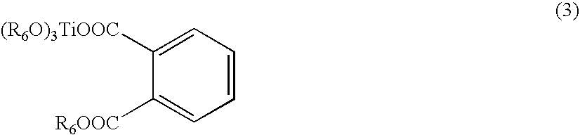
- an organic electroluminescent device including: an organic electroluminescent device, comprising: a pair of electrodes; and an organic layer interposed between the pair of electrodes, the organic layer comprising a layer formed of a titanium oxide derivative represented by Formulae 1 through 4: Ti(OR 1 ) 4 (1)
- FIG. 1 is a sectional view of an organic electroluminescent device according to an embodiment of the present invention.
- An organic electroluminescent device has high luminescent efficiency and a long lifetime, and can be easily and economically manufactured.
- the organic electroluminescent device includes an organic layer interposed between a pair of electrodes, in which the organic layer includes a layer formed by coating a titanium oxide derivative solution or includes a layer doped with a titanium oxide derivative.
- the titanium oxide derivative may be represented by one of Formulae 1 through 4: Ti(OR 1 ) 4 (1) where R 1 is CH 3 CO—CH ⁇ CCH 3 —, C 2 H 5 OCO—CH ⁇ CCH 3 —, —CH 3 CH—COO ⁇ NH4 + , —COR 2 , —CO(C 6 H 4 )COOR 3 , or a C 1 -C 12 alkyl group; where
- R 2 is a substituted or unsubstituted C 1 -C 12 alkyl group
- R 3 is a substituted or unsubstituted C 1 -C 12 alkyl group
- R 4 is a substituted or unsubstituted C 1 -C 12 alkyl group
- R 5 is a substituted or unsubstituted C 1 -C 12 alkyl group
- R 6 is a substituted or unsubstituted C 1 -C 12 alkyl group
- R 7 is a substituted or unsubstituted C 1 -C 12 alkyl group.
- the titanium oxide derivative represented by one of Formulae 1, 2, 3 and 4 may be, but is not limited to, tetraisopropyl titanate, tetra-n-butyl titanate, tetrakis(2-ethylhexyl)titanate, acetylacetonate titanate chelate, ethyl acetoacetate titanate chelate, triethanolamine titanate chelate, lactic acid titanate chelate ammonium salt, or the like.
- the substituted or unsubstituted C 1 -C 12 alkyl group used in the present embodiment is an alkyl group having at least one hydrogen atom substituted with a halogen atom, a hydroxy group, a nitro group, a cyano group, a substituted or unsubstituted amino group (—NH 2 , —NH(R), —N(R′)(R′′) where R′ and R′′ are each independently a C 1 -C 10 alkyl group), an amidino group, a hydrazine group, a hydrazone group, a carboxyl group, a sulfonic acid group, a phosphoric acid group, a C 1 -C 20 alkyl group, a C 1 -C 20 halogenated alkyl group, a C 2 -C 20 alkenyl group, a C 2 -C 20 alkynyl group, a C 1 -C 20 hetero alkyl group, a C 6 -C
- organic layers interposed between the pair of electrodes includes at least one layer selected from a hole injection layer, a hole transport layer, an emissive layer, and an electron transport layer.
- the titanium oxide derivative can be coated between these organic layers as a separate layer, or these organic layers can be doped with the titanium oxide derivative.
- an organic layer such as a hole injection layer, a hole transport layer, an emissive layer, or an electron transport layer can be doped with the titanium oxide derivative.
- the emissive layer containing the titanium oxide derivative may have a thickness of 10 nm to 100 nm. When the thickness of the emissive layer is less than 10 nm, the lifetime of the organic electroluminescent device may be reduced, whereas when the thickness of the emissive layer is greater than 100 nm, the operating voltage of the organic electroluminescent device increases.
- the titanium oxide derivative can be formed into a layer. That is, the titanium oxide derivative can be coated as a separate layer between organic layers, such as a hole injection layer, a hole transport layer, an emissive layer, or an electron transport layer. That is, it means that the titanium oxide derivative can be formed in addition to a hole injection layer, a hole transport layer, an emissive layer, and/or an electron transport layer.
- the titanium oxide derivative can be formed into a layer.
- Such a coating layer can be formed using a conventional wet coating method including spin coating and drying processes.
- a titanium oxide derivative is formed into a layer, and then the prepared layer is transferred by thermal deposition, laser deposition, heat bar, magnetic induction heating, or ultrasonic friction.
- a solution of the titanium oxide derivative can be prepared using a solvent selected from alcohols, aromatic groups, dimethyl formamid, acetone, and a mixture of these.
- the solvent is not limited thereto.
- a concentration of the solution of the titanium oxide derivative in the organic electroluminescent device may be in the range of 1 wt % to 90 wt %.
- a material used to form the hole injection layer of the organic electroluminescent device is not limited.
- examples of such a material include copper phthalocyanine (CuPc); a starburst-type amine, such as TCTA, m-MTDATA, IDE406 (commercially available from Idemitsu Inc.), polyaniline/dodecylbenzenesulfonic acid (Pani/DBSA), or poly(3,4-ethylenedioxythiophene)/poly(4-styrenesulfonate) (PEDOT/PSS); and the like.
- the material used to form the hole injection layer is not limited thereto.
- a material used to form the hole transport layer of the organic electroluminescent device according to an embodiment of the present invention is not limited.
- examples of such a material include 1,3,5-tricarbazolylbenzene, 4,4′-biscarbazolylbiphenyl, polyvinylcarbazole, m-biscarbazolylbenzene, 4,4′-biscarbazolyl-2,2′-dimethylbiphenyl, 4,4′,4′′-tri( N-carbazolyl )triphenylamine, 1,3,5-tri(2-carbazolylphenyl)benzene, 1,3,5-tris(2-carbazolyl-5-methoxyphenyl)benzene, bis(4-carbazolylphenyl)silane, N,N′-bis(3-methylphenyl)-N,N′-diphenyl-[1,1-biphenyl]-4,4′diamine(TPD), N,N′-di(
- a material used to form the emissive layer of the organic electroluminescent device according to an embodiment of the present invention is not limited.
- Examples of a material used to form a red emissive layer include DCM1, DCM2, Eu(thenoyltrifluoroacetone) 3 (Eu(TTA) 3 ), dicyanomethylene-2-butyl-6-(1,1,7,7,-tetramethyljulolidyl-9-enyl)-4H-pyran(DCJTB), and the like. Meanwhile, the red emissive layer can be formed using various methods.
- Alq 3 can be doped with a dopant such as DCJTB; Alq 3 and rubrene are co-deposited and then doped with a dopant; or 4,4′-N-N′-dicarbazole-biphenyl (CBP) can be doped with a dopant such as BTPIr.
- a dopant such as DCJTB
- Alq 3 and rubrene are co-deposited and then doped with a dopant
- CBP 4,4′-N-N′-dicarbazole-biphenyl
- a green emissive layer can be formed using, for example, coumarin 6, C545T, quinacridone, Ir(ppy) 3 , or the like.
- the green emissive layer can be formed using various methods.
- CBP can be used using a dopant such as Ir(ppy) 3 , or a host such as Alq 3 and a dopant such as a coumarin-based material can be used.
- the coumarin-based material can be C314S, C343S, C7, C7S, C6, C6S, C314T, or C545T.
- a blue emissive layer can be formed using, for example, oxadiazole dimer dyes (Bis-DAPOXP)), spiro compounds (Spiro-DPVBi, Spiro-6P), triarylamine compounds, bis(styryl)amine(DPVBi, DSA), Compound(A), bis[2-(4,6-difluorophenyl)pyridinato-N,C 2′ ] iridium picolinate (FIrpic), CzTT, anthracene, 1,1,4,4-tetraphenyl-1,3-butadiene (TPB), 3,5,3′,5′-tetrakis-tert-butyldiphenoquione; 1,2,3,4,5-pentaphenyl-1,3-cyclopentadiene (PPCP), DST, TPA, OXD-4, BBOT, AZM-Zn, BH-013X (commercially available from Idemitsu Inc.) which is an aromatic hydrocarbon compound
- the thickness of the emissive layer may be in the range of 100 ⁇ to 1000 ⁇ , preferably 100 ⁇ to 500 ⁇ . Meanwhile, the red, green, and blue emissive layers may have the same or different thicknesses. When the thickness of the emissive layer is less than 100 ⁇ , the lifetime of the organic electroluminescent device may be reduced. On the other hand, when the thickness of the emissive layer is greater than 1000 ⁇ , the driving voltage of the organic electroluminescent device may be increased significantly.
- a material used to form an electron transport layer of the organic electroluminescent device according to an embodiment of the present invention is not limited and can be Alq 3 .
- the thickness of the electron transport layer may be in the range of 100 ⁇ to 400 ⁇ , preferably 250 ⁇ to 350 ⁇ . When the thickness of the electron transport layer is less than 100 ⁇ , electrons can be transported very quickly so that a charge balance can be broken. On the other hand, when the thickness of the electron transport layer is greater than 400 ⁇ , the driving voltage of the device can be increased.
- FIG. 1 is a sectional view of an organic electroluminescent device according to an embodiment of the present invention.
- an anode is formed on a substrate.
- the substrate can be any substrate that is commonly used in an organic electroluminescent device.
- the substrate can be a glass substrate or a plastic substrate, both of which are transparent and waterproof, have plane surfaces, and can be easily handled.
- the anode can be a reflective electrode formed using a highly conductive metal, such as lithium (Li), magnesium (Mg), aluminum (Al), aluminum-lithium (Al—Li), calcium (Ca), magnesium-indium (Mg—In), magnesium-silver (Mg—Ag), calcium (Ca)-aluminum(Al), aluminum (Al)-ITO, or the like.
- HIL hole injection layer
- HTL hole transport layer
- EML emissive layer
- a hole blocking material is vacuum deposited or spin coated on the emissive layer to selectively form a hole blocking layer (HBL).
- the hole blocking material is not limited and can be any material that has an electron transporting capability and higher ionization potential than luminescent compounds used to form the emissive layer (EML).
- Examples of the hole blocking material may include bis(2-methyl-8-quinolato)-(p-phenylphenolato)-aluminum (Balq), bathocuproine (BCP), and tris(N-arylbenzimidazole) (TPBI), etc.
- the thickness of the hole blocking layer (HBL) may be in the range of 30 ⁇ to 60 ⁇ , preferably 40 ⁇ to 50 ⁇ . When the thickness of the hole blocking layer (HBL) is less than 30 ⁇ , it is difficult to block holes. On the other hand, when the thickness of the hole blocking layer is greater than 60 ⁇ , the operating voltage of the organic electroluminescent device can be increased.
- An electron transporting material can be vacuum deposited or spin coated on the emissive layer (EML) or the hole blocking layer (HBL) to selectively form an electron transport layer (ETL). Then, a material used to form an electron injection layer (EIL) can be vacuum deposited or spin coated on the emissive layer (EML), the hole blocking layer (HBL), or the electron transport layer (ETL).
- the material used to form the electron injection layer (EIL) can be BaF 2 , LiF, NaCl, CsF, Li 2 O, BaO, or the like, but is not limited thereto.
- the thickness of the electron injection layer (EIL) may be in the range of 2 ⁇ to 10 ⁇ , preferably 2 ⁇ to 5 ⁇ , and more preferably 2 ⁇ to 4 ⁇ .
- the thickness of the electron injection layer (EIL) is less than 2 ⁇ , the electron injection efficiency may decrease.
- the thickness of the electron injection layer (EIL) is greater than 10 ⁇ , the operating voltage of the organic electroluminescent device may increase.
- the organic electroluminescent device according to the embodiment of the present invention can be used in various kinds of flat panel display devices, for example, a passive organic electroluminescent display device and an active organic electroluminescent display device.
- an active organic electroluminescent display device includes the organic electroluminescent device according to the embodiment of the present invention
- the anode can be electrically connected to a source electrode or drain electrode of a thin film transistor.
- a 1,300 ⁇ -thick substrate (aluminum and ITO)(commercially available from SDI Co. Ltd.) used as a reflective anode was cut to a size of 50 mm ⁇ 50 mm ⁇ 0.7 mm.
- the prepared substrate was ultrasonically cleaned in isopropyl alcohol for 5 minutes, ultrasonically cleaned in pure water for 5 minutes, cleaned using ultraviolet (UV) rays for 30 minutes, and then cleaned using ozone.
- a hole injection layer having a thickness of 1,000 ⁇ was formed on the anode using m-TDATA that was used as a hole injecting material.
- NPB that was used as a hole transporting material was deposited on the hole injection layer to form a hole transport layer having a thickness of 1,200 ⁇ .
- CBP and bis[2-(2′-benzothienyl)-pyridinato-N,C 3 ′] iridium (BPTIr) that were used as red luminescent materials were deposited on the hole transport layer to form an emissive layer having a thickness of 300 ⁇ .
- a titanium oxide derivative tetraisopropyl titanate
- 100 g of butanol was dissolved in 100 g of butanol to prepare a solution of the titanium oxide derivative.
- the prepared solution was spin coated on the emissive layer to a thickness of 30 nm.
- Balq was deposited on the emissive layer to form a hole blocking layer having a thickness of 50 ⁇ .
- Alq 3 was deposited on the hole blocking layer to form an electron transport layer having a thickness of 250 ⁇ .
- LiF was deposited on the electron transport layer to form an electron injection layer having a thickness of 3 ⁇ .
- Mg:Ag was deposited on the electron injection layer to form a cathode having a thickness of 100 ⁇ .
- An organic electroluminescent device in which a titanium oxide derivative was contained in the emissive layer was manufactured having the following structure: ITO/PEDOT(500 ⁇ )/emissive layer(700 ⁇ )/Ba(50 ⁇ )/Al(2,000 ⁇ ).
- an anode (positive electrode) an ITO glass substrate (15 ⁇ /cm 2 ,1500 ⁇ ) commercially available from Corning Co. was cut to a size of 50 mm ⁇ 50 mm ⁇ 0.7 mm, and then was ultrasonically cleaned in isopropyl alcohol for 5 minutes, ultrasonically cleaned in pure water for 5 minutes, cleaned using ultraviolet (UV) rays for 30 minutes, and then cleaned using ozone.
- UV ultraviolet
- PEDOT/PSS product name: Al 4083, commercially available from Bayer Co.
- a polymer solution of PEDOT/PSS product name: Al 4083, commercially available from Bayer Co.
- a hole injecting material was spin coated on the anode to a thickness of 500 ⁇ .
- 1 g of a green 223 used as a green luminescent material (commercially available from Dow Inc.) dissolved in 10 g of toluene was mixed with 1 g of tetra-n-butyltitanate used as a titanium oxide derivative dissolved in 10 g of butanol.
- the prepared mixed solution was spin coated to a thickness of 700 ⁇ to form an emissive layer.
- a 1300 ⁇ -thick substrate (aluminum and ITO)(commercially available from SDI Co. Ltd.) used as a reflective anode was cut to a size of 50 mm ⁇ 50 mm ⁇ 0.7 mm.
- the prepared substrate was ultrasonically cleaned in isopropyl alcohol for 5 minutes, ultrasonically cleaned in pure water for 5 minutes, cleaned using ultraviolet (UV) rays for 30 minutes, and then cleaned using ozone.
- a hole injection layer having a thickness of 1000 ⁇ was formed on the anode using m-TDATA that was used as a hole injecting material.
- NPB that was used as a hole transporting material was deposited on the hole injection layer to form a hole transport layer having a thickness of 1200 ⁇ .
- CBP and BPTIr that were used as red luminescent materials were deposited on the hole transport layer to form an emissive layer having a thickness of 300 ⁇ .
- Balq was deposited on the emissive layer to form a hole blocking layer having a thickness of 50 ⁇ , and then Alq 3 was deposited on the hole blocking layer to form an electron transport layer having a thickness of 250 ⁇ .
- Mg:Ag was deposited thereon to a thickness of 100 ⁇ to form a cathode. As a result, an organic electroluminescent device was manufactured.
- An organic electroluminescent device was manufactured in the same manner as in Example 1, except that the tetraisopropyltitanate that was used as a titanium oxide derivative was not coated on the emissive layer.
- An organic electroluminescent device was manufactured in the same manner as in Example 2, except that the tetra-n-butyltitanate that was used as a titanium oxide derivative was not mixed with the green 223.
- An organic electroluminescent device was manufactured in the same manner as in Example 3, except that the tetrakis(2-ethylhexyl)titanate that was used as a titanium oxide derivative was not spin coated on the electron transport layer.
- the organic electroluminescent devices prepared according to Examples 1 through 3 has a lower operating voltage, higher maximum luminescent efficiency, and longer lifetime than the organic electroluminescent devices prepared according to Comparative Examples 1 through 3 which respectively correspond to Examples 1 through 3.
- an organic electroluminescent device that has higher luminescent efficiency, longer lifetime and a lower operating voltage than a conventional organic electroluminescent device can be easily manufactured.
Landscapes
- Chemical & Material Sciences (AREA)
- Engineering & Computer Science (AREA)
- Materials Engineering (AREA)
- Crystallography & Structural Chemistry (AREA)
- Inorganic Chemistry (AREA)
- Organic Chemistry (AREA)
- Electroluminescent Light Sources (AREA)
Abstract
Description
Ti(OR1)4 (1)
-
- where R1 is each independently CH3CO—CH═CCH3—, C2H5OCO—CH═CCH3—, —CH3CH—COO−NH4+, —COR2, —CO(C6H4)COOR3, or a C1-C12 alkyl group;
- R2 is a substituted or unsubstituted C1-C12 alkyl group; and
- R3 is a substituted or unsubstituted C1-C12 alkyl group;
- where R1 is each independently CH3CO—CH═CCH3—, C2H5OCO—CH═CCH3—, —CH3CH—COO−NH4+, —COR2, —CO(C6H4)COOR3, or a C1-C12 alkyl group;

-
- where R4 is a substituted or unsubstituted C1-C12 alkyl group; and
- R5 is a substituted or unsubstituted C1-C12 alkyl group;
- where R4 is a substituted or unsubstituted C1-C12 alkyl group; and

-
- where R6 is a substituted or unsubstituted C1-C12 alkyl group; and

-
- where R7 is a substituted or unsubstituted C1-C12 alkyl group.
Ti(OR1)4 (1)
where R1 is CH3CO—CH═CCH3—, C2H5OCO—CH═CCH3—, —CH3CH—COO−NH4+, —COR2, —CO(C6H4)COOR3, or a C1-C12 alkyl group; where

where R4 is a substituted or unsubstituted C1-C12 alkyl group; and

where R6 is a substituted or unsubstituted C1-C12 alkyl group; and

where R7 is a substituted or unsubstituted C1-C12 alkyl group.


| TABLE 1 | ||||
| Operating | ||||
| (Turn-on) | Maximum | |||
| Voltage/ | Luminescent | |||
| Voltage at | Efficiency | |||
| 100 cd/m2 (V) | (cd/A) | Lifetime | ||
| Example 1 | 2.3/3.0 | 10.3 @ 6.8 V | 105 | khr@1000 cd/m2 |
| Example 2 | 2.7/3.7 | 20.2 @ 6.3 V | 1820 | hr@1000 cd/m2 |
| Example 3 | 2.6/3.0 | 5.1 @ 6.5 V | 99 | khr@1000 cd/m2 |
| Comparative | 3.1/6.0 | 7.8 @ 6.3 V | 58 | khr@1000 cd/m2 |
| Example 1 | ||||
| Comparative | 3.2/5.0 | 11.0 @ 7.6 V | 430 | hr@1000 cd/m2 |
| Example 2 | ||||
| Comparative | 3.3/6.2 | 2.1 @ 6.8 V | 55 | khr@1000 cd/m2 |
| Example 3 | ||||
Claims (18)
Ti(OR1)4 (1)


Ti(OR1)4 (1)


Ti(OR1)4 (1)


Applications Claiming Priority (2)
| Application Number | Priority Date | Filing Date | Title |
|---|---|---|---|
| KR10-2006-0009032 | 2006-01-27 | ||
| KR1020060009032A KR101234227B1 (en) | 2006-01-27 | 2006-01-27 | An organic electroluminescent device |
Publications (2)
| Publication Number | Publication Date |
|---|---|
| US20070178331A1 US20070178331A1 (en) | 2007-08-02 |
| US8227092B2 true US8227092B2 (en) | 2012-07-24 |
Family
ID=38322433
Family Applications (1)
| Application Number | Title | Priority Date | Filing Date |
|---|---|---|---|
| US11/633,005 Active 2029-12-26 US8227092B2 (en) | 2006-01-27 | 2006-12-04 | Organic electroluminescent device |
Country Status (4)
| Country | Link |
|---|---|
| US (1) | US8227092B2 (en) |
| JP (1) | JP5207630B2 (en) |
| KR (1) | KR101234227B1 (en) |
| CN (1) | CN101009361A (en) |
Cited By (2)
| Publication number | Priority date | Publication date | Assignee | Title |
|---|---|---|---|---|
| US20100276687A1 (en) * | 2007-12-21 | 2010-11-04 | Sukekazu Aratani | Organic electroluminescent display device |
| US20110175072A1 (en) * | 2010-01-20 | 2011-07-21 | Canon Kabushiki Kaisha | Organic light-emitting device |
Families Citing this family (8)
| Publication number | Priority date | Publication date | Assignee | Title |
|---|---|---|---|---|
| US7994711B2 (en) * | 2005-08-08 | 2011-08-09 | Semiconductor Energy Laboratory Co., Ltd. | Light emitting device and manufacturing method thereof |
| KR101255232B1 (en) * | 2006-01-27 | 2013-04-16 | 삼성디스플레이 주식회사 | A composition for an electron transporting layer, an electron transporting layer prepared therefrom, and an organic electroluminescence device comprising the electron transmitting layer |
| KR101407581B1 (en) * | 2007-10-09 | 2014-06-16 | 삼성디스플레이 주식회사 | Organic light emitting device and manufacturing method thereof |
| KR101213493B1 (en) | 2010-04-13 | 2012-12-20 | 삼성디스플레이 주식회사 | Organic light emitting device and method for fabricating the same |
| CN102169966B (en) * | 2011-04-28 | 2013-05-15 | 中国科学院长春应用化学研究所 | an organic light emitting diode |
| TWI569491B (en) * | 2012-10-11 | 2017-02-01 | Joled Inc | Organic EL display device and manufacturing method thereof, ink and electronic machine |
| CN104009176A (en) * | 2013-02-26 | 2014-08-27 | 海洋王照明科技股份有限公司 | Organic electroluminescent device and preparation method |
| WO2014133141A1 (en) * | 2013-02-28 | 2014-09-04 | 日本放送協会 | Organic electroluminescence element |
Citations (10)
| Publication number | Priority date | Publication date | Assignee | Title |
|---|---|---|---|---|
| JPH09148071A (en) | 1995-11-20 | 1997-06-06 | Bayer Ag | Intermediate layer of electroluminescence arrangement containing fine powder inorganic particles |
| US5643685A (en) * | 1993-10-26 | 1997-07-01 | Fuji Xerox Co., Ltd. | Thin film electroluminescence element and process for producing the same |
| US5656252A (en) * | 1994-01-28 | 1997-08-12 | Elf Aquitaine Production | Process for obtaining zeolites containing titanium |
| JPH10199681A (en) | 1997-01-08 | 1998-07-31 | Kansai Shin Gijutsu Kenkyusho:Kk | Thin film light emitting device and method of manufacturing the same |
| US5869199A (en) | 1993-03-26 | 1999-02-09 | Sumitomo Electric Industries, Ltd. | Organic electroluminescent elements comprising triazoles |
| JPH11307267A (en) | 1998-04-16 | 1999-11-05 | Tdk Corp | Organic el element |
| JP2002252089A (en) | 2001-02-26 | 2002-09-06 | Bando Chem Ind Ltd | Double-sided organic electroluminescence device |
| US6447934B1 (en) | 1998-10-09 | 2002-09-10 | Denso Corporation | Organic electroluminescent panel |
| US20030129451A1 (en) * | 2001-10-18 | 2003-07-10 | Fuji Xerox Co., Ltd. | Organic electroluminescence device |
| US20030160235A1 (en) * | 2002-02-27 | 2003-08-28 | Katsura Hirai | Organic thin-film transistor and manufacturing method for the same |
Family Cites Families (7)
| Publication number | Priority date | Publication date | Assignee | Title |
|---|---|---|---|---|
| JPS5873154A (en) * | 1981-10-26 | 1983-05-02 | Hitachi Chem Co Ltd | Semiconductor composition |
| JP4607268B2 (en) * | 1999-08-02 | 2011-01-05 | パナソニック株式会社 | Organic electroluminescence device |
| JP2001185359A (en) * | 1999-12-24 | 2001-07-06 | Teikoku Tsushin Kogyo Co Ltd | EL element dielectric paste and method of manufacturing the same |
| JP2003208984A (en) * | 2001-11-09 | 2003-07-25 | Ricoh Co Ltd | Electroluminescent device and light wavelength conversion method |
| JP2005216686A (en) * | 2004-01-29 | 2005-08-11 | Morio Taniguchi | Method for manufacturing organic electroluminescence device |
| JP4513060B2 (en) * | 2004-09-06 | 2010-07-28 | 富士電機ホールディングス株式会社 | Organic EL device |
| JP2006190995A (en) * | 2004-12-06 | 2006-07-20 | Semiconductor Energy Lab Co Ltd | Composite material comprising organic compound and inorganic compound, light emitting element and light emitting device employing the composite material as well as manufacturing method of the light emitting element |
-
2006
- 2006-01-27 KR KR1020060009032A patent/KR101234227B1/en not_active Expired - Fee Related
- 2006-12-04 US US11/633,005 patent/US8227092B2/en active Active
-
2007
- 2007-01-15 CN CNA200710002019XA patent/CN101009361A/en active Pending
- 2007-01-17 JP JP2007008344A patent/JP5207630B2/en not_active Expired - Fee Related
Patent Citations (11)
| Publication number | Priority date | Publication date | Assignee | Title |
|---|---|---|---|---|
| US5869199A (en) | 1993-03-26 | 1999-02-09 | Sumitomo Electric Industries, Ltd. | Organic electroluminescent elements comprising triazoles |
| US5643685A (en) * | 1993-10-26 | 1997-07-01 | Fuji Xerox Co., Ltd. | Thin film electroluminescence element and process for producing the same |
| US5656252A (en) * | 1994-01-28 | 1997-08-12 | Elf Aquitaine Production | Process for obtaining zeolites containing titanium |
| JPH09148071A (en) | 1995-11-20 | 1997-06-06 | Bayer Ag | Intermediate layer of electroluminescence arrangement containing fine powder inorganic particles |
| US5917279A (en) | 1995-11-20 | 1999-06-29 | Bayer Aktiengesllschaft | Intermediate layer in electroluminescent arrangements containing finely divided inorganic particles |
| JPH10199681A (en) | 1997-01-08 | 1998-07-31 | Kansai Shin Gijutsu Kenkyusho:Kk | Thin film light emitting device and method of manufacturing the same |
| JPH11307267A (en) | 1998-04-16 | 1999-11-05 | Tdk Corp | Organic el element |
| US6447934B1 (en) | 1998-10-09 | 2002-09-10 | Denso Corporation | Organic electroluminescent panel |
| JP2002252089A (en) | 2001-02-26 | 2002-09-06 | Bando Chem Ind Ltd | Double-sided organic electroluminescence device |
| US20030129451A1 (en) * | 2001-10-18 | 2003-07-10 | Fuji Xerox Co., Ltd. | Organic electroluminescence device |
| US20030160235A1 (en) * | 2002-02-27 | 2003-08-28 | Katsura Hirai | Organic thin-film transistor and manufacturing method for the same |
Non-Patent Citations (1)
| Title |
|---|
| Young Kwan Kim et al., "Size dependence of electroluminescence of nanoparticle (rutile-TiO2) dispersed MEH-PPV films", Synthetic Metals 111-112 (2000) 207-211. |
Cited By (4)
| Publication number | Priority date | Publication date | Assignee | Title |
|---|---|---|---|---|
| US20100276687A1 (en) * | 2007-12-21 | 2010-11-04 | Sukekazu Aratani | Organic electroluminescent display device |
| US8476618B2 (en) | 2007-12-21 | 2013-07-02 | Hitachi, Ltd. | Organic electroluminescent display device |
| US20110175072A1 (en) * | 2010-01-20 | 2011-07-21 | Canon Kabushiki Kaisha | Organic light-emitting device |
| US8330153B2 (en) * | 2010-01-20 | 2012-12-11 | Canon Kabushiki Kaisha | Organic light-emitting device |
Also Published As
| Publication number | Publication date |
|---|---|
| US20070178331A1 (en) | 2007-08-02 |
| KR101234227B1 (en) | 2013-02-18 |
| JP5207630B2 (en) | 2013-06-12 |
| KR20070078614A (en) | 2007-08-01 |
| JP2007201462A (en) | 2007-08-09 |
| CN101009361A (en) | 2007-08-01 |
Similar Documents
| Publication | Publication Date | Title |
|---|---|---|
| US8227092B2 (en) | Organic electroluminescent device | |
| US7776457B2 (en) | Organic electroluminescent device | |
| KR100670383B1 (en) | Organic light emitting device and flat panel display device having the same | |
| US9478754B2 (en) | Phenylcarbazole-based compounds and fluorene-based compounds and organic light emitting device and flat panel display device comprising the same | |
| US9150783B2 (en) | Organic light emitting diode including organic layer comprising organic metal complex | |
| US7968214B2 (en) | White organic light emitting device | |
| US7777408B2 (en) | Organic light-emitting device | |
| US20060199038A1 (en) | Organic electroluminescent device and method of manufacturing the same | |
| US8247090B2 (en) | Heterocyclic compound and organic electroluminescent device comprising the same | |
| JP4722695B2 (en) | Organic light emitting device | |
| US20070285010A1 (en) | Organic light emitting device | |
| US20060222888A1 (en) | Organic light-emitting device and method of manufacturing the same | |
| JP5073208B2 (en) | Organic electroluminescent device and manufacturing method thereof | |
| US20090218934A1 (en) | Organic light-emitting device | |
| US20060263631A1 (en) | Organic light-emitting device | |
| US8632893B2 (en) | Organic compound and organic electroluminescence device employing the same | |
| US20090085470A1 (en) | Organic light emitting device | |
| TW201448309A (en) | Organic light-emitting device and flat panel display device therewith | |
| US20060182995A1 (en) | Biphenyl derivatives and organic electroluminescent devices using the same | |
| US20080286606A1 (en) | Organic light emitting diode and flat panel device including the same | |
| KR20110024695A (en) | Organic light emitting diode | |
| KR100730221B1 (en) | Organic light emitting device and flat panel display device having the same | |
| KR20150076031A (en) | Heterocyclic compounds and organic light emitting diode device comprising the same | |
| KR20090129853A (en) | Anthracene Derivatives and Organic Electroluminescent Devices Employing the Same | |
| KR101407581B1 (en) | Organic light emitting device and manufacturing method thereof |
Legal Events
| Date | Code | Title | Description |
|---|---|---|---|
| AS | Assignment |
Owner name: SAMSUNG SDI CO., LTD., A CORPORATION ORGANIZED UND Free format text: ASSIGNMENT OF ASSIGNORS INTEREST;ASSIGNORS:PARK, JONG-JIN;KIM, YU-JIN;PARK, SANG-HOON;AND OTHERS;REEL/FRAME:018671/0061 Effective date: 20061127 |
|
| AS | Assignment |
Owner name: SAMSUNG MOBILE DISPLAY CO., LTD., KOREA, REPUBLIC Free format text: ASSIGNMENT OF ASSIGNORS INTEREST;ASSIGNOR:SAMSUNG SDI CO., LTD.;REEL/FRAME:022034/0001 Effective date: 20081210 Owner name: SAMSUNG MOBILE DISPLAY CO., LTD.,KOREA, REPUBLIC O Free format text: ASSIGNMENT OF ASSIGNORS INTEREST;ASSIGNOR:SAMSUNG SDI CO., LTD.;REEL/FRAME:022034/0001 Effective date: 20081210 |
|
| FEPP | Fee payment procedure |
Free format text: PAYOR NUMBER ASSIGNED (ORIGINAL EVENT CODE: ASPN); ENTITY STATUS OF PATENT OWNER: LARGE ENTITY |
|
| STCF | Information on status: patent grant |
Free format text: PATENTED CASE |
|
| AS | Assignment |
Owner name: SAMSUNG DISPLAY CO., LTD., KOREA, REPUBLIC OF Free format text: MERGER;ASSIGNOR:SAMSUNG MOBILE DISPLAY CO., LTD.;REEL/FRAME:029241/0599 Effective date: 20120702 |
|
| FPAY | Fee payment |
Year of fee payment: 4 |
|
| MAFP | Maintenance fee payment |
Free format text: PAYMENT OF MAINTENANCE FEE, 8TH YEAR, LARGE ENTITY (ORIGINAL EVENT CODE: M1552); ENTITY STATUS OF PATENT OWNER: LARGE ENTITY Year of fee payment: 8 |
|
| MAFP | Maintenance fee payment |
Free format text: PAYMENT OF MAINTENANCE FEE, 12TH YEAR, LARGE ENTITY (ORIGINAL EVENT CODE: M1553); ENTITY STATUS OF PATENT OWNER: LARGE ENTITY Year of fee payment: 12 |